WO2022209663A1 - 半導体装置 - Google Patents
半導体装置 Download PDFInfo
- Publication number
- WO2022209663A1 WO2022209663A1 PCT/JP2022/010283 JP2022010283W WO2022209663A1 WO 2022209663 A1 WO2022209663 A1 WO 2022209663A1 JP 2022010283 W JP2022010283 W JP 2022010283W WO 2022209663 A1 WO2022209663 A1 WO 2022209663A1
- Authority
- WO
- WIPO (PCT)
- Prior art keywords
- semiconductor device
- main
- lead
- semiconductor element
- sealing resin
- Prior art date
- Legal status (The legal status is an assumption and is not a legal conclusion. Google has not performed a legal analysis and makes no representation as to the accuracy of the status listed.)
- Ceased
Links
Images











Classifications
-
- H—ELECTRICITY
- H10—SEMICONDUCTOR DEVICES; ELECTRIC SOLID-STATE DEVICES NOT OTHERWISE PROVIDED FOR
- H10W—GENERIC PACKAGES, INTERCONNECTIONS, CONNECTORS OR OTHER CONSTRUCTIONAL DETAILS OF DEVICES COVERED BY CLASS H10
- H10W70/00—Package substrates; Interposers; Redistribution layers [RDL]
- H10W70/40—Leadframes
- H10W70/481—Leadframes for devices being provided for in groups H10D8/00 - H10D48/00
-
- H—ELECTRICITY
- H10—SEMICONDUCTOR DEVICES; ELECTRIC SOLID-STATE DEVICES NOT OTHERWISE PROVIDED FOR
- H10D—INORGANIC ELECTRIC SEMICONDUCTOR DEVICES
- H10D8/00—Diodes
- H10D8/20—Breakdown diodes, e.g. avalanche diodes
- H10D8/25—Zener diodes
-
- H—ELECTRICITY
- H10—SEMICONDUCTOR DEVICES; ELECTRIC SOLID-STATE DEVICES NOT OTHERWISE PROVIDED FOR
- H10W—GENERIC PACKAGES, INTERCONNECTIONS, CONNECTORS OR OTHER CONSTRUCTIONAL DETAILS OF DEVICES COVERED BY CLASS H10
- H10W70/00—Package substrates; Interposers; Redistribution layers [RDL]
- H10W70/40—Leadframes
- H10W70/411—Chip-supporting parts, e.g. die pads
-
- H—ELECTRICITY
- H10—SEMICONDUCTOR DEVICES; ELECTRIC SOLID-STATE DEVICES NOT OTHERWISE PROVIDED FOR
- H10W—GENERIC PACKAGES, INTERCONNECTIONS, CONNECTORS OR OTHER CONSTRUCTIONAL DETAILS OF DEVICES COVERED BY CLASS H10
- H10W70/00—Package substrates; Interposers; Redistribution layers [RDL]
- H10W70/40—Leadframes
- H10W70/421—Shapes or dispositions
- H10W70/424—Cross-sectional shapes
-
- H—ELECTRICITY
- H10—SEMICONDUCTOR DEVICES; ELECTRIC SOLID-STATE DEVICES NOT OTHERWISE PROVIDED FOR
- H10W—GENERIC PACKAGES, INTERCONNECTIONS, CONNECTORS OR OTHER CONSTRUCTIONAL DETAILS OF DEVICES COVERED BY CLASS H10
- H10W72/00—Interconnections or connectors in packages
-
- H—ELECTRICITY
- H10—SEMICONDUCTOR DEVICES; ELECTRIC SOLID-STATE DEVICES NOT OTHERWISE PROVIDED FOR
- H10W—GENERIC PACKAGES, INTERCONNECTIONS, CONNECTORS OR OTHER CONSTRUCTIONAL DETAILS OF DEVICES COVERED BY CLASS H10
- H10W74/00—Encapsulations, e.g. protective coatings
- H10W74/10—Encapsulations, e.g. protective coatings characterised by their shape or disposition
- H10W74/111—Encapsulations, e.g. protective coatings characterised by their shape or disposition the semiconductor body being completely enclosed
-
- H—ELECTRICITY
- H10—SEMICONDUCTOR DEVICES; ELECTRIC SOLID-STATE DEVICES NOT OTHERWISE PROVIDED FOR
- H10W—GENERIC PACKAGES, INTERCONNECTIONS, CONNECTORS OR OTHER CONSTRUCTIONAL DETAILS OF DEVICES COVERED BY CLASS H10
- H10W90/00—Package configurations
- H10W90/811—Multiple chips on leadframes
-
- H—ELECTRICITY
- H10—SEMICONDUCTOR DEVICES; ELECTRIC SOLID-STATE DEVICES NOT OTHERWISE PROVIDED FOR
- H10W—GENERIC PACKAGES, INTERCONNECTIONS, CONNECTORS OR OTHER CONSTRUCTIONAL DETAILS OF DEVICES COVERED BY CLASS H10
- H10W90/00—Package configurations
- H10W90/701—Package configurations characterised by the relative positions of pads or connectors relative to package parts
- H10W90/751—Package configurations characterised by the relative positions of pads or connectors relative to package parts of bond wires
- H10W90/753—Package configurations characterised by the relative positions of pads or connectors relative to package parts of bond wires between laterally-adjacent chips
Definitions
- the present disclosure relates to semiconductor devices.
- Patent Document 1 discloses an example of a conventional semiconductor device.
- the semiconductor device disclosed in the document includes a plurality of leads, semiconductor elements and sealing resin.
- a semiconductor element (6) is mounted on the leads (3).
- Other leads (1, 2) different from the lead (3) on which the semiconductor element is mounted are arranged in a direction (x) perpendicular to the thickness direction (z) of the lead (3) with respect to the lead (3). are spaced apart.
- the sealing resin (8) partially covers the plurality of leads and the semiconductor element, and has a rectangular shape when viewed in the thickness direction (z).
- the semiconductor device described in Patent Document 1 is surface-mounted, for example, on circuit boards of various devices.
- a circuit board on which the semiconductor device is mounted may warp due to the influence of heat or the like.
- stress acts on the sealing resin and the leads. If a large stress acts between the leads separated from each other in the direction x in the sealing resin, there is concern that the sealing resin may peel off from the leads or crack in the sealing resin.
- the present disclosure has been conceived under the circumstances described above, and has an object to provide a semiconductor device suitable for suppressing peeling of the sealing resin.
- a semiconductor device provided by the present disclosure includes a first lead having a first main surface facing one side in the thickness direction and a first back surface facing the other side, and a second main surface facing the one side in the thickness direction. and a second back surface facing the other side, the second lead being spaced apart from the first lead on one side in a first direction orthogonal to the thickness direction, the first main surface and a second semiconductor element arranged on the second main surface, a part of the first lead, a part of the second lead, the first semiconductor element and the second semiconductor element. and a sealing resin that covers the semiconductor element.
- the first semiconductor element and the second semiconductor element each have a first element side surface facing one side in the first direction and a second element side surface facing the other side.
- the first lead extends from the first direction center section of the sealing resin equidistant from the first element side surface of the first semiconductor element and the second element side surface of the second semiconductor element in the first direction. a first main portion positioned on the other side in the first direction; and a first extension portion extending from the first main portion to the one side in the first direction.
- the second lead includes a second main portion positioned on one side in the first direction with respect to the first direction central section.
- FIG. 1 is a perspective view showing a semiconductor device according to a first embodiment of the present disclosure
- FIG. FIG. 2 is a perspective view (through sealing resin) showing the semiconductor device according to the first embodiment of the present disclosure.
- FIG. 5 is a front view of the semiconductor device shown in FIG. 1.
- FIG. 6 is a right side view of the semiconductor device shown in FIG. 1.
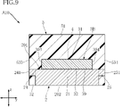
- FIG. FIG. 7 is a cross-sectional view along line VII-VII of FIG.
- FIG. 10 is a diagram showing the circuit configuration of the semiconductor device according to the first embodiment of the present disclosure
- 11 is a cross-sectional view, similar to FIG. 7, showing a state in which the semiconductor device shown in FIG. 1 is mounted on a circuit board.
- 12 is a plan view, similar to FIG. 3, showing a semiconductor device according to a first modification of the first embodiment
- FIG. 13 is a front view of the semiconductor device shown in FIG. 12.
- FIG. FIG. 14 is a plan view, similar to FIG. 3, showing a semiconductor device according to a second modification of the first embodiment.
- 15 is a front view of the semiconductor device shown in FIG. 14.
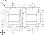
- FIG. 16 is a plan view, similar to FIG. 3, showing a semiconductor device according to a third modification of the first embodiment;
- FIG. 17 is a front view of the semiconductor device shown in FIG. 16.
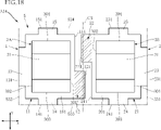
- FIG. 18 is a plan view, similar to FIG. 3, showing a semiconductor device according to a fourth modification of the first embodiment;
- FIG. 19 is a front view of the semiconductor device shown in FIG. 18.
- FIG. 20 is a plan view, similar to FIG. 3, showing a semiconductor device according to a fifth modification of the first embodiment.
- 21 is a front view of the semiconductor device shown in FIG. 20.
- a certain entity A is formed on a certain entity B” and “a certain entity A is formed on a certain entity B” mean “a certain entity A is formed on a certain entity B”. It includes "being directly formed in entity B” and “being formed in entity B while another entity is interposed between entity A and entity B”.
- ⁇ an entity A is placed on an entity B'' and ⁇ an entity A is located on an entity B'' mean ⁇ an entity A is located on an entity B.'' It includes "directly placed on B” and "some entity A is placed on an entity B while another entity is interposed between an entity A and an entity B.”
- ⁇ an object A is located on an object B'' means ⁇ an object A is adjacent to an object B and an object A is positioned on an object B. and "the thing A is positioned on the thing B while another thing is interposed between the thing A and the thing B".
- ⁇ an object A overlaps an object B when viewed in a certain direction'' means ⁇ an object A overlaps all of an object B'' and ⁇ an object A overlaps an object B.'' It includes "overlapping a part of a certain thing B".
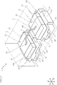
- a semiconductor device A10 of this embodiment includes a first lead 1, a second lead 2, a first semiconductor element 3A, a second semiconductor element 3B, a conductive member 4, and a sealing resin 5.
- the package format of the semiconductor device A10 is QFN (Quad For Non-Lead Package).
- FIG. 1 is a perspective view showing the semiconductor device A10.
- FIG. 2 is a perspective view showing the semiconductor device A10.
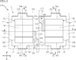
- FIG. 3 is a plan view showing the semiconductor device A10.
- FIG. 4 is a bottom view showing the semiconductor device A10.
- FIG. 5 is a front view showing the semiconductor device A10.
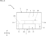
- FIG. 6 is a right side view showing the semiconductor device A10.
- FIG. 7 is a cross-sectional view along line VII-VII of FIG.
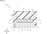
- FIG. 8 is a cross-sectional view along line VIII-VIII of FIG.
- FIG. 9 is a circuit configuration diagram of the semiconductor device A10. 2 and 3 are transparent through the sealing resin 5 for convenience of understanding.
- the permeated sealing resin 5 is indicated by an imaginary line (chain double-dashed line).
- the conducting member 4 is omitted.
- the semiconductor device A10 shown in these figures is surface-mounted on circuit boards of various devices.
- the shape of the semiconductor device A10 when viewed in the thickness direction is rectangular.
- the thickness direction of the semiconductor device A10 is called "thickness direction z”.
- a direction perpendicular to the thickness direction z and along one side of the semiconductor device A10 (horizontal direction in FIG. 3) is called a “first direction x”.
- a direction perpendicular to both the thickness direction z and the first direction x (vertical direction in FIG. 3) is called a “second direction y”.
- the size of the semiconductor device A10 is not particularly limited.
- the vertical direction z dimension is about 0.15 to 1.0 mm.
- first lead 1 and the second lead 2 are formed, for example, by punching or etching a metal plate.
- First lead 1 and second lead 2 are made of, for example, either Cu (copper) or Ni (nickel), or an alloy thereof.
- Each of the first lead 1 and the second lead 2 is partially covered with the sealing resin 5 .
- the first lead 1 is arranged on the left side of the semiconductor device A10 in the drawing (the other side in the first direction x).
- the second lead 2 is arranged on the right side of the semiconductor device A10 in the drawing (one side in the first direction x).
- the first lead 1 and the second lead 2 are arranged apart from each other in the first direction x.
- the first lead 1 has a first major surface 101, a first rear surface 102 and a first concave surface 103.
- the first major surface 101 faces one side in the thickness direction z.
- the first main surface 101 is covered with the sealing resin 5 .
- the first rear surface 102 and the first concave surface 103 face the side opposite to the first major surface 101 (the other side in the thickness direction z).
- the first rear surface 102 is exposed from the sealing resin 5 .
- the first concave surface 103 is located closer to one side in the thickness direction z than the first back surface 102 and closer to the first main surface 101 than the first back surface 102 is.
- the first concave surface 103 overlaps a part of the first major surface 101 when viewed in the thickness direction z.
- the first concave surface 103 is positioned on one side in the first direction x relative to the first rear surface 102 when viewed in the thickness direction z.
- the first concave surface 103 is covered with the sealing resin 5 .
- the first concave surface 103 is formed, for example, by half-etching.
- the first lead 1 includes a first main portion 11 , a first extending portion 12 , a first terminal portion 13 , a first connecting portion 14 and a second connecting portion 15 .
- the first main portion 11 has a rectangular shape when viewed in the thickness direction z.
- the first main portion 11 is located on the left side (the other side in the first direction x) of the center of the semiconductor device A10 in the first direction x.
- the first main portion 11 includes a portion of the first main surface 101, a portion of the first rear surface 102, a portion of the first concave surface 103 and a first inner surface 111.
- a first main surface 101 of the first main portion 11 is a portion on which the first semiconductor element 3A is mounted.
- the first rear surface 102 of the first main portion 11 is a portion that becomes a rear surface terminal.
- the first inner surface 111 is positioned at one side end of the first main portion 11 in the first direction x and faces one side in the first direction x.
- the first inner surface 111 connects to both the first major surface 101 and the first concave surface 103 .
- the first extending portion 12 is connected to the first main portion 11 and extends from the first inner surface 111 of the first main portion 11 to one side in the first direction x. In the present embodiment, the first extending portion 12 extends to one side in the first direction x from a portion of the first main portion 11 that is closer to one side in the second direction y. In FIG. 3, the first extending portion 12 is hatched.
- the first extending portion 12 includes a portion of the first main surface 101, a portion of the first concave surface 103, a first tip surface 121, a first curved surface 122 and a It has a first intermediate surface 123 .
- the first tip surface 121 is positioned at one side end of the first extending portion 12 in the first direction x and faces one side in the first direction x.
- the first tip surface 121 connects to both the first major surface 101 and the first concave surface 103 .
- the first tip surface 121 is located in the center of the semiconductor device A10 in the first direction x.
- the first curved surface 122 is an arc-shaped concave surface when viewed in the thickness direction z.
- the first curved surface 122 connects both the first main surface 101 and the first concave surface 103 and the first distal surface 121 .
- the first intermediate surface 123 faces one side in the first direction x.
- the first intermediate surface 123 is located between the first tip surface 121 and the first inner surface 111 of the first main portion 11 in the first direction x.
- the first intermediate surface 123 is located on the other side in the second direction y with respect to the first tip end surface 121 .
- the first intermediate surface 123 connects both the first major surface 101 and the first concave surface 103 and the first curved surface 122 .
- the first terminal portion 13 is connected to the first main portion 11 and has a rectangular shape when viewed in the thickness direction z.
- the first terminal portion 13 is connected to the other end of the first main portion 11 in the first direction x.
- the dimension of the first terminal portion 13 in the second direction y is smaller than the dimension of the first main portion 11 in the second direction y.
- the first terminal portion 13 is positioned at the center of the first main portion 11 in the second direction y when viewed in the first direction x.
- the first terminal portion 13 has a portion of the first main surface 101 , a portion of the first rear surface 102 and a first end surface 131 .
- the first end face 131 is located at the other side end of the first terminal portion 13 in the first direction x and faces the other side in the first direction x.
- the first end surface 131 is exposed from the sealing resin 5 .
- the first connecting portion 14 is connected to the first main portion 11 and has a rectangular shape when viewed in the thickness direction z.
- the first connecting portion 14 is connected to one end of the first main portion 11 in the second direction y.
- the dimension of the first connecting portion 14 in the first direction x is smaller than the dimension of the first main portion 11 in the first direction x.
- the first connecting portion 14 is positioned in the center of the first main portion 11 in the first direction x when viewed in the second direction y.
- the first connecting portion 14 has a first connecting portion end surface 141 .
- the first connecting portion end face 141 is located at one side end of the first connecting portion 14 in the second direction y and faces one side in the second direction y.
- the first connecting portion end surface 141 is exposed from the sealing resin 5 .
- the second connecting portion 15 is connected to the first main portion 11 and has a rectangular shape when viewed in the thickness direction z.
- the second connecting portion 15 connects to the other end of the first main portion 11 in the second direction y.
- the dimension of the second connecting portion 15 in the first direction x is smaller than the dimension of the first main portion 11 in the first direction x.
- the second connecting portion 15 is positioned at the center of the first main portion 11 in the first direction x when viewed in the second direction y.
- the second connecting portion 15 has a second connecting portion end surface 151 .
- the second connecting portion end surface 151 is located at the other side end of the second connecting portion 15 in the second direction y and faces the other side in the second direction y.
- the second connecting portion end surface 151 is exposed from the sealing resin 5 .
- the second lead 2 has a second main surface 201, a second rear surface 202 and a second concave surface 203.
- the second main surface 201 faces one side in the thickness direction z.
- the second main surface 201 is at the same position as the first main surface 101 of the first lead 1 in the thickness direction z.
- the second principal surface 201 is covered with the sealing resin 5 .
- the second rear surface 202 and the second concave surface 203 face the side opposite to the second major surface 201 (the other side in the thickness direction z).
- the second rear surface 202 is exposed from the sealing resin 5 .
- the second concave surface 203 is positioned closer to one side in the thickness direction z than the second back surface 202 and closer to the second major surface 201 than the second back surface 202 is.
- the second concave surface 203 overlaps a part of the second major surface 201 when viewed in the thickness direction z.
- the second concave surface 203 is positioned on the other side in the first direction x of the second back surface 202 when viewed in the thickness direction z.
- the second concave surface 203 is covered with the sealing resin 5 .
- the second concave surface 203 is formed, for example, by half-etching.
- the second lead 2 includes a second main portion 21 , a second extension portion 22 , a second terminal portion 23 , a third connecting portion 24 and a fourth connecting portion 25 .
- the second main portion 21 has a rectangular shape when viewed in the thickness direction z.
- the second main portion 21 is located on the right side (one side in the first direction x) of the center of the semiconductor device A10 in the first direction x.
- the first main portion 11 and the second main portion 21 of the first lead 1 described above are separated in the first direction x, and are symmetrical with respect to the center of the semiconductor device A10 in the first direction x (see FIG. 3). symmetrical).
- the second main portion 21 includes a portion of the second main surface 201, a portion of the second rear surface 202, a portion of the second concave surface 203, and a second inner surface 211.
- a second main surface 201 of the second main portion 21 is a portion on which the second semiconductor element 3B is mounted.
- a second rear surface 202 of the second main portion 21 is a portion that becomes a rear surface terminal.
- the second inner surface 211 is located at the other side end of the second main portion 21 in the first direction x and faces the other side in the first direction x.
- the second inner surface 211 connects to both the second major surface 201 and the second concave surface 203 .
- the second extending portion 22 is connected to the second main portion 21 and extends from the second inner surface 211 of the second main portion 21 to the other side in the first direction x.
- the second extending portion 22 extends to the other side in the first direction x from a portion of the second main portion 21 closer to the other side in the second direction y.
- the second extending portion 22 is hatched.
- the second extending portion 22 includes a portion of the second main surface 201, a portion of the second concave surface 203, a second tip surface 221, a second curved surface 222 and a It has a second intermediate surface 223 .
- the second tip surface 221 is positioned at the other side end in the first direction x of the second extending portion 22 and faces the other side in the first direction x.
- the second tip surface 221 connects to both the second major surface 201 and the second concave surface 203 .
- the second tip surface 221 is positioned in the center of the semiconductor device A10 in the first direction x.
- the second curved surface 222 is an arc-shaped concave curved surface when viewed in the thickness direction z.
- the second curved surface 222 connects to both the second major surface 201 and the second concave surface 203 and the second tip surface 221 .
- the second intermediate surface 223 faces the other side in the first direction x.
- the second intermediate surface 223 is positioned between the second tip surface 221 and the second inner surface 211 of the second main portion 21 in the first direction x.
- the second intermediate surface 223 is located on one side in the second direction y relative to the second tip surface 221 .
- a second intermediate surface 223 connects both the second major surface 201 and the second concave surface 203 and the second curved surface 222 .
- the second terminal portion 23 is connected to the second main portion 21 and has a rectangular shape when viewed in the thickness direction z.
- the second terminal portion 23 is connected to one side end of the second main portion 21 in the first direction x when viewed in the first direction x.
- the dimension of the second terminal portion 23 in the second direction y is smaller than the dimension of the second main portion 21 in the second direction y.
- the second terminal portion 23 is positioned at the center of the second main portion 21 in the second direction y when viewed in the first direction x.
- the second terminal portion 23 has a portion of the second main surface 201 , a portion of the second rear surface 202 and a second end surface 231 .
- the second end face 231 is located at one side end of the second terminal portion 23 in the first direction x and faces one side in the first direction x.
- the second end surface 231 is exposed from the sealing resin 5 .
- the third connecting portion 24 is connected to the second main portion 21 and has a rectangular shape when viewed in the thickness direction z.
- the third connecting portion 24 connects to one side end of the second main portion 21 in the second direction y.
- the dimension of the third connecting portion 24 in the first direction x is smaller than the dimension of the second main portion 21 in the first direction x.
- the third connecting portion 24 is positioned at the center of the second main portion 21 in the first direction x when viewed in the second direction y.
- the third connecting portion 24 has a third connecting portion end surface 241 .
- the third connecting portion end face 241 is located at one side end of the third connecting portion 24 in the second direction y and faces one side in the second direction y.
- the third connecting portion end surface 241 is exposed from the sealing resin 5 .
- the fourth connecting portion 25 is connected to the second main portion 21 and has a rectangular shape when viewed in the thickness direction z.
- the fourth connecting portion 25 connects to the other end of the second main portion 21 in the second direction y.
- the dimension of the fourth connecting portion 25 in the first direction x is smaller than the dimension of the first main portion 11 in the first direction x.
- the second connecting portion 15 is positioned at the center of the second main portion 21 in the first direction x when viewed in the second direction y.
- the fourth connecting portion 25 has a fourth connecting portion end surface 251 .
- the fourth connecting portion end face 251 is positioned at the other side end in the second direction y of the fourth connecting portion end face 251 and faces the other side in the second direction y.
- the fourth connecting portion end surface 251 is exposed from the sealing resin 5 .
- the first semiconductor element 3A and the second semiconductor element 3B are elements that exhibit electrical functions of the semiconductor device A10.
- the types of first semiconductor element 3A and second semiconductor element 3B are not particularly limited.
- the two first semiconductor elements 3A and the second semiconductor elements 3B are elements of the same type, and both are Zener diodes.
- each of the first semiconductor element 3A and the second semiconductor element 3B has a rectangular shape when viewed in the thickness direction z.
- the first semiconductor element 3A is arranged on the first main surface 101 of the first main portion 11 (first lead 1).
- the first semiconductor element 3 ⁇ /b>A has a first element side surface 301 , a second element side surface 302 , a third element side surface 303 , a fourth element side surface 304 , a first electrode 31 and a second electrode 32 .
- Each of the first element side surface 301, the second element side surface 302, the third element side surface 303, and the fourth element side surface 304 is formed on a surface facing one side and a surface facing the other side in the thickness direction z of the first semiconductor element 3A. It is sandwiched and connected to both the surface facing one side in the thickness direction z and the surface facing the other side.
- the first element side surface 301 faces one side in the first direction x.
- the second element side surface 302 faces the other side in the first direction x.
- the third element side surface 303 faces one side in the second direction y.
- the fourth element side surface 304 faces the other side in the second direction y.
- the first electrode 31 is provided on the surface facing one side in the thickness direction z of the first semiconductor element 3A.
- the second electrode 32 is provided on the surface of the first semiconductor element 3A facing the other side in the thickness direction z.
- the first electrode 31 is an anode (cathode) and the second electrode 32 is a cathode (cathode).
- the first semiconductor element 3A is electrically joined to the first main surface 101 (first main portion 11, first lead 1) via a conductive joint material 39. As shown in FIG.
- the conductive bonding material 39 electrically connects the first main surface 101 and the second electrode 32 .
- a constituent material of the conductive bonding material 39 is not particularly limited, and examples thereof include solder, metal paste material, or sintered metal.
- the second semiconductor element 3B is arranged on the second main surface 201 of the second main portion 21 (second lead 2).
- the second semiconductor element 3 ⁇ /b>B has a first element side surface 301 , a second element side surface 302 , a third element side surface 303 , a fourth element side surface 304 , a first electrode 31 and a second electrode 32 .
- Each of the first element side surface 301, the second element side surface 302, the third element side surface 303, and the fourth element side surface 304 is formed on a surface facing one side and a surface facing the other side in the thickness direction z of the second semiconductor element 3B. It is sandwiched and connected to both the surface facing one side in the thickness direction z and the surface facing the other side.
- the first element side surface 301 faces one side in the first direction x.
- the second element side surface 302 faces the other side in the first direction x.
- the third element side surface 303 faces one side in the second direction y.
- the fourth element side surface 304 faces the other side in the second direction y.
- the first electrode 31 is provided on the surface of the second semiconductor element 3B facing one side in the thickness direction z.
- the second electrode 32 is provided on the surface of the second semiconductor element 3B facing the other side in the thickness direction z.
- the first electrode 31 is an anode (cathode) and the second electrode 32 is a cathode (cathode).
- the second semiconductor element 3B is electrically joined to the second main surface 201 (the second main portion 21, the second leads 2) via the conductive joint material 39. As shown in FIG.
- the conductive bonding material 39 electrically connects the second main surface 201 and the second electrode 32 .
- a constituent material of the conductive bonding material 39 is not particularly limited, and examples thereof include solder, metal paste material, or sintered metal.
- the conduction member 4 provides conduction between the first electrode 31 of the first semiconductor element 3A and the first electrode 31 of the second semiconductor element 3B.
- a specific configuration of the conducting member 4 is not limited at all, and examples thereof include wires and ribbons made of metal.
- Examples of the metal forming the conducting member 4 include metals such as Au (gold) and Al (aluminum), and alloys thereof. In the present embodiment, the case in which one conductive member 4 is provided is exemplified, but the configuration may be such that two or more conductive members 4 are provided.
- FIG. 10 is a diagram showing the circuit configuration of the semiconductor device A10 of this embodiment.
- the first semiconductor element 3A and the second semiconductor element 3B are connected in series in opposite directions. In the configuration shown in the figure, even if a voltage higher than the breakdown voltage is applied between the first lead 1 and the second lead 2 in any direction, a constant voltage is applied to the first semiconductor element 3A and the second semiconductor element 3B. current flows.
- the sealing resin 5 partially covers the first lead 1 and the second lead 2, the first semiconductor element 3A and the second semiconductor element 3B, and the conduction member 4.
- Sealing resin 5 is made of, for example, black epoxy resin.
- the sealing resin 5 has a resin main surface 51, a resin back surface 52, a first resin side surface 531, a second resin side surface 532, a third resin side surface 533, and a fourth resin side surface. 534.
- the resin main surface 51 and the resin back surface 52 face opposite sides in the thickness direction z and are separated from each other.
- the resin main surface 51 faces one side in the thickness direction z.
- the resin back surface 52 faces the other side in the thickness direction z.
- the first back surface 102 of the first lead 1 and the second back surface 202 of the second lead 2 are exposed from the resin back surface 52 so as to be flush with the resin back surface 52 .
- first resin side surface 531 , second resin side surface 532 , third resin side surface 533 , and fourth resin side surface 534 is sandwiched between resin main surface 51 and resin back surface 52 . lead to both.
- the first resin side surface 531 and the second resin side surface 532 face opposite sides in the first direction x and are separated from each other.
- the first resin side surface 531 faces one side in the first direction x.
- the second resin side surface 532 faces the other side in the first direction x.
- the second end surface 231 of the second lead 2 is exposed from the first resin side surface 531 so as to be flush with the first resin side surface 531 .
- the first end surface 131 of the first lead 1 is exposed from the second resin side surface 532 so as to be flush with the second resin side surface 532 .
- the third resin side surface 533 and the fourth resin side surface 534 face opposite sides in the second direction y and are separated from each other.
- the third resin side surface 533 faces one side in the second direction y.
- the fourth resin side surface 534 faces the other side in the second direction y.
- the first connecting portion end surface 141 of the first lead 1 and the third connecting portion end surface 241 of the second lead 2 are exposed from the third resin side surface 533 so as to be flush with the third resin side surface 533 .
- the second connecting portion end surface 151 of the first lead 1 and the fourth connecting portion end surface 251 of the second lead 2 are exposed from the fourth resin side surface 534 so as to be flush with the fourth resin side surface 534 .
- the cross section of the sealing resin 5 equidistant from the first element side surface 301 of the first semiconductor element 3A and the second element side surface 302 of the second semiconductor element 3B in the first direction x is indicated by a dashed line.
- the first main portion 11 of the first lead 1 is positioned on the other side (left side in FIG. 7) in the first direction x with respect to the first direction central section CS.
- the second main portion 21 of the second lead 2 is positioned on one side (right side in FIG. 7) in the first direction x with respect to the first direction central section CS.
- the first main portion 11 and the second main portion 21 are separated from each other in the first direction x with the first direction central section CS interposed therebetween. As shown in FIG. 3, the first main portion 11 and the second main portion 21 are arranged symmetrically (left-right symmetrical in FIG. 3) across the first direction center section CS when viewed in the thickness direction z. . In the present embodiment, the first distal end surface 121 of the first extending portion 12 overlaps the first direction central section CS. Also, the second end surface 221 of the second extending portion 22 overlaps with the first direction central section CS.
- the first tip end face 121 (the second tip face 221) overlaps with the first direction central section CS" means that the tip face 121 (221) strictly overlaps with the first direction central section CS.
- the concept includes errors that may occur due to the manufacturing accuracy of the leads 1 and 2 and the sealing resin 5 . This also applies to modified examples described later with reference to FIG. 12 onward.
- FIG. 11 is a cross-sectional view showing a state in which the semiconductor device A10 is mounted on the circuit board 6.
- Semiconductor device A10 is bonded to circuit wiring (not shown) formed on circuit board 6 via solder 7, for example.
- the first rear surface 102 and the second rear surface 202 are exposed from the sealing resin 5 as rear terminals, and are joined to the circuit wiring by the solder 7.
- the first end face 131 and the second end face 231 are exposed from the sealing resin 5 as terminals, and a solder fillet 71 is formed between the first end face 131 and the second end face 231 and the circuit board.
- the circuit board 6 on which the semiconductor device A10 is mounted may warp due to the influence of heat or the like.
- the sealing resin 5 has the first A relatively large stress acts on the portion between the first main portion 11 of the first lead 1 and the second main portion 21 of the second lead 2 in the direction x.
- the first lead 1 includes a first extending portion 12.
- the first extending portion 12 extends from the first main portion 11 located on the other side in the first direction x with respect to the first direction central cross section CS of the sealing resin 5 and extends on one side (second main portion) in the first direction x. portion 21).
- the first end surface 121 of the first extending portion 12 overlaps with the first direction central section CS of the sealing resin 5. As shown in FIG. According to such a configuration, the first extending portion 12 reaches the center of the sealing resin 5 in the first direction x. preferable.
- the second lead 2 includes a second extending portion 22.
- the second extending portion 22 extends from the second main portion 21 located on one side in the first direction x with respect to the first direction central cross section CS of the sealing resin 5, to the other side in the first direction x (first main portion). portion 11).
- stress can be further reduced. Therefore, peeling of the sealing resin 5 from the leads 1 and 2 can be effectively suppressed.
- the second end surface 221 of the second extending portion 22 overlaps the first direction central cross section CS of the sealing resin 5. As shown in FIG. According to such a configuration, the second extending portion 22 reaches the center of the sealing resin 5 in the first direction x, so that peeling of the sealing resin 5 from the leads 1 and 2 is prevented. more preferred.
- the first extending portion 12 of the first lead 1 and the second extending portion 22 of the second lead 2 are positioned on one side and the other side of the second direction y when viewed in the first direction x. According to such arrangement of the first extension portion 12 and the second extension portion 22, the first lead 1 (the first main portion 11 and the first extension 12) and the second lead 2 (the second main portion 21 and the second extension 22) can be prevented from coming too close in the first direction x. Therefore, the semiconductor device A10 has a preferable package structure for increasing strength while suppressing an increase in package size and a decrease in withstand voltage.
- the first lead 1 has a first concave surface 103 facing away from the thickness direction z.
- First main portion 11 and first extension portion 12 each include a portion of first concave surface 103 .
- the first concave surface 103 is covered with the sealing resin 5 .
- the second lead 2 has a second concave surface 203 facing away from the thickness direction z.
- Second main portion 21 and second extension portion 22 each include a portion of second concave surface 203 .
- the second concave surface 203 is covered with the sealing resin 5 .
- the first semiconductor element 3A arranged on the first main surface 101 (first main portion 11) and the second semiconductor element 3B arranged on the second main surface 201 (second main portion 21) are elements of the same type. (Zener diode).
- the first main portion 11 and the second main portion 21 supporting the first semiconductor element 3A and the second semiconductor element 3B sandwich the first direction central section CS of the sealing resin 5 when viewed in the thickness direction z. symmetrical (left-right symmetrical in FIG. 3).
- the first electrodes 31 of the semiconductor elements 3A and 3B are electrically connected by the conductive member 4. As shown in FIG.
- first extending portion 12 and the second extending portion 22 located between the first main portion 11 and the second main portion 21 are not connected to a conductive member (wire or the like) and are electrically connected. It has no role of conducting pathway.
- the semiconductor device A10 has a package structure with increased strength. form.
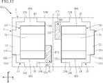
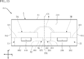
- FIG. 12 and 13 show a semiconductor device according to a first modified example of the first embodiment.
- FIG. 12 is a plan view similar to FIG. 3 shown in the above embodiment.
- 13 is a front view of the semiconductor device shown in FIG. 12.
- FIG. 12 elements identical or similar to those of the semiconductor device A10 of the above-described embodiment are assigned the same reference numerals as those of the above-described embodiment, and description thereof will be omitted as appropriate.
- the shapes of the first extension portion 12 and the second extension portion 22 are different from those of the semiconductor device A10 of the above embodiment.
- both the first extending portion 12 and the second extending portion 22 are rectangular when viewed in the thickness direction z.
- the first extending portion 12 has a portion of the first major surface 101 , a portion of the first concave surface 103 and a first tip surface 121 .
- the first tip surface 121 is located on the other side in the first direction x (left side in FIG. 12) of the first direction central cross section CS of the sealing resin 5 .
- the second extending portion 22 has a portion of the second major surface 201 , a portion of the second concave surface 203 and a second tip surface 221 .
- the second tip surface 221 is located on one side (right side in FIG. 12) in the first direction x of the first direction center section CS of the sealing resin 5 .
- the first lead 1 includes the first extending portion 12 also in the semiconductor device A11 of this modified example.
- the first extending portion 12 extends from the first main portion 11 located on the other side in the first direction x with respect to the first direction central cross section CS of the sealing resin 5 and extends on one side (second main portion) in the first direction x. portion 21).
- the portion of the sealing resin 5 between the first main portion 11 and the first extending portion 12 is subjected to a large stress. can be reduced. Therefore, peeling of the sealing resin 5 from the leads 1 and 2 can be suppressed.
- the same effects as those of the above embodiment can be obtained.
- FIG. 14 and 15 show a semiconductor device according to a second modification of the first embodiment.
- FIG. 14 is a plan view similar to FIG. 3 shown in the above embodiment.
- 15 is a front view of the semiconductor device shown in FIG. 14.
- FIG. 14 is a plan view similar to FIG. 3 shown in the above embodiment.
- the shapes of the first extension portion 12 and the second extension portion 22 are different from those of the semiconductor device A10 of the above embodiment.
- the first extending portion 12 and the second extending portion 22 do not have the first intermediate surface 123 and the second intermediate surface 223, and both are rectangular portions when viewed in the thickness direction z. It is a shape that combines a concave curve part.
- the first extending portion 12 has a portion of the first major surface 101 , a portion of the first concave surface 103 , a first tip surface 121 and a first curved surface 122 .
- the first tip surface 121 overlaps the first direction center section CS of the sealing resin 5 .
- the second extending portion 22 has a portion of the second major surface 201 , a portion of the second concave surface 203 , a second tip surface 221 and a second curved surface 222 .
- the second tip surface 221 overlaps the first direction center section CS of the sealing resin 5 .
- the first lead 1 includes the first extending portion 12 also in the semiconductor device A12 of this modified example.
- the first extending portion 12 extends from the first main portion 11 located on the other side in the first direction x with respect to the first direction central cross section CS of the sealing resin 5 and extends on one side (second main portion) in the first direction x. portion 21).
- the portion of the sealing resin 5 between the first main portion 11 and the first extending portion 12 is subjected to a large stress. can be reduced. Therefore, peeling of the sealing resin 5 from the leads 1 and 2 can be suppressed.
- the same effects as those of the above embodiment can be obtained.
- FIG. 16 and 17 show a semiconductor device according to a third modified example of the first embodiment.
- FIG. 16 is a plan view similar to FIG. 3 shown in the above embodiment.
- 17 is a front view of the semiconductor device shown in FIG. 16.
- FIG. 16 is a plan view similar to FIG. 3 shown in the above embodiment.
- the shape of the first extension portion 12 is different from that of the semiconductor device A10 of the above embodiment.
- the semiconductor device A13 does not have the second extension 22 of the semiconductor device A10 of the above embodiment.
- the first extending portion 12 has a rectangular shape when viewed in the thickness direction z.
- the first extending portion 12 has a portion of the first major surface 101 , a portion of the first concave surface 103 and a first tip surface 121 .
- the first tip surface 121 overlaps the first direction center section CS of the sealing resin 5 .
- the semiconductor device A13 of this modified example also has the same effects as those of the above-described embodiment within the range of the configuration similar to that of the semiconductor device A10 of the above-described embodiment.
- FIG. 18 and 19 show a semiconductor device according to a third modification of the first embodiment.
- FIG. 18 is a plan view similar to FIG. 3 shown in the above embodiment.
- 19 is a front view of the semiconductor device shown in FIG. 18.
- FIG. 18 is a plan view similar to FIG. 3 shown in the above embodiment.
- the shapes of the first extension portion 12 and the second extension portion 22 are different from those of the semiconductor device A10 of the above embodiment.
- both the first extending portion 12 and the second extending portion 22 are rectangular when viewed in the thickness direction z.
- the first extending portion 12 has a portion of the first major surface 101 , a portion of the first concave surface 103 and a first tip surface 121 .
- the first tip surface 121 is positioned on one side (right side in FIG. 18) in the first direction x of the first direction center section CS of the sealing resin 5 .
- the second extending portion 22 has a portion of the second major surface 201 , a portion of the second concave surface 203 and a second tip surface 221 .
- the second tip surface 221 is positioned on the other side in the first direction x (left side in FIG. 18) of the first direction center section CS of the sealing resin 5 .
- the semiconductor device A14 of this modified example also has the same effects as those of the above-described embodiment within the range of the configuration similar to that of the semiconductor device A10 of the above-described embodiment.
- the first extending portion 12 extends from the first main portion 11 located on the other side in the first direction x with respect to the first direction central section CS, and extends through the first direction central section CS. It extends to one side in the first direction x from the first direction central section CS.
- the second extending portion 22 extends from the second main portion 21 located on one side in the first direction x with respect to the first direction central section CS, and penetrates the first direction central section CS to extend toward the first direction central section CS. It extends to the other side in the first direction x from the cross section CS.
- the semiconductor device A14 having such a configuration has a more preferable package structure in terms of increasing strength.
- FIG. 20 and 21 show a semiconductor device according to the fifth modification of the first embodiment.
- FIG. 20 is a plan view similar to FIG. 3 shown in the above embodiment.
- 21 is a front view of the semiconductor device shown in FIG. 20.
- FIG. 20 is a plan view similar to FIG. 3 shown in the above embodiment.
- the shape and arrangement of the first extending portion 12 and the second extending portion 22 are different from those of the semiconductor device A10 of the above embodiment.
- the first lead 1 includes a plurality of (two in the illustrated example) first extensions 12 .
- the second lead 2 includes a plurality of (two in the illustrated example) second extensions 22 .
- Each of the plurality of first extensions 12 and the plurality of second extensions 22 has a rectangular shape when viewed in the thickness direction z. When viewed in the first direction x, the first extensions 12 and the second extensions 22 are alternately arranged along the second direction y.
- the multiple first extensions 12 each have a portion of the first main surface 101 , a portion of the first concave surface 103 and a first tip surface 121 .
- the first tip surface 121 overlaps the first direction center section CS of the sealing resin 5 .
- Each of the plurality of second extensions 22 has a portion of the second main surface 201 , a portion of the second concave surface 203 and a second tip surface 221 .
- the second tip surface 221 overlaps the first direction center section CS of the sealing resin 5 .
- the semiconductor device A15 of this modified example also has the same effect as the above-described embodiment within the range of the configuration similar to that of the semiconductor device A10 of the above-described embodiment.
- the semiconductor device according to the present disclosure is not limited to the above-described embodiments.
- the specific configuration of each part of the semiconductor device according to the present disclosure can be changed in various ways.
- the package format of the semiconductor device A10 and the like is QFN, but the package format of the semiconductor device is not limited to this.
- the semiconductor device of the present disclosure may be applied to a QFP (Quad Flat Package) in which leads protrude from the side surface of the sealing resin.
- first rear surface 102 of the first main portion 11 and the second rear surface 202 of the second main portion 21 are exposed from the sealing resin 5 and function as rear terminals has been described, but the present invention is not limited to this. .
- a configuration in which the first back surface 102 and the second back surface 202 do not function as back surface terminals may be employed.
- Appendix 1 a first lead having a first main surface facing one side in the thickness direction and a first back surface facing the other side; It has a second principal surface facing one side in the thickness direction and a second back surface facing the other side, and is spaced from the first lead to one side in a first direction orthogonal to the thickness direction.
- a positioned second lead a first semiconductor element arranged on the first main surface and a second semiconductor element arranged on the second main surface; a sealing resin that covers part of the first lead, part of the second lead, the first semiconductor element, and the second semiconductor element; each of the first semiconductor element and the second semiconductor element has a first element side surface facing one side in the first direction and a second element side surface facing the other side;
- the first lead extends from the first direction center section of the sealing resin equidistant from the first element side surface of the first semiconductor element and the second element side surface of the second semiconductor element in the first direction.
- the semiconductor device wherein the second lead includes a second main portion located on one side in the first direction with respect to the central section in the first direction.
- the first extending portion has a first distal end face facing one side in the first direction
- the semiconductor device according to appendix 1 wherein the first tip end surface overlaps with the first direction center section or is located on one side of the first direction center section with respect to the first direction center section.
- the first main portion has a first inner surface facing one side in the first direction, 3.
- Appendix 4. The semiconductor device according to any one of appendices 1 to 3, wherein the second lead includes the second extension portion extending from the second main portion to the other side in the first direction.
- the second extending portion has a second distal end face facing the other side in the first direction, 5.
- the semiconductor device according to appendix 4 wherein the second tip end surface overlaps with the first direction central section or is located on the other side in the first direction with respect to the first direction central section.
- Appendix 6. The second main portion has a second inner surface facing the other side in the first direction, 6.
- the first extending portion and the second extending portion are positioned on one side and the other side of a second direction orthogonal to both the thickness direction and the first direction when viewed in the first direction, 6.
- Appendix 8. the first extending portion has a first intermediate surface facing one side in the first direction and positioned between the first tip surface and the first inner surface in the first direction; Supplementary note 7, wherein the second extending portion has a second intermediate surface facing the other side of the first direction and positioned between the second tip surface and the second inner surface in the first direction.
- the first intermediate surface is located on the other side in the second direction relative to the first tip surface
- the semiconductor device according to appendix 8, wherein the second intermediate surface is located on one side of the second end surface in the second direction.
- Appendix 10. The semiconductor device according to any one of Appendixes 7 to 9, wherein the first main surface and the second main surface are at the same position in the thickness direction.
- Appendix 11. The semiconductor device according to any one of appendices 1 to 10, wherein the first rear surface and the second rear surface are exposed from the sealing resin.
- Appendix 12. 12 The semiconductor device according to appendix 11, wherein the first main portion and the second main portion are arranged symmetrically with respect to the first direction central section when viewed in the thickness direction. Appendix 13.
- the first lead has a first concave surface facing the other side in the thickness direction and covered with the sealing resin;
- the first main portion includes a portion of the first main surface, a portion of the first concave surface, and at least a portion of the first back surface, 13.
- Appendix 14. the second lead has a second concave surface facing the other side in the thickness direction and covered with the sealing resin; the second main portion includes a portion of the second main surface, a portion of the second concave surface, and at least a portion of the first rear surface; 14.
- A10, A11, A12, A13, A14, A15 semiconductor device 1: first lead 101: first main surface 102: first rear surface 103: first concave surface 11: first main portion 111: first inner surface 12: second 1 Extension Part 121: First Tip Surface 122: First Curved Surface 123: First Intermediate Surface 13: First Terminal Part 131: First End Surface 14: First Connection Part 141: First Connection Part End Surface 15: Second Connecting part 151 : Second connecting part end surface 2 : Second lead 201 : Second main surface 202 : Second back surface 203 : Second concave surface 21 : Second main part 211 : Second inner surface 22 : Second extension part 221 : Second tip surface 222: Second curved surface 223: Second intermediate surface 24: Third connecting portion 241: Third connecting portion end surface 25: Fourth connecting portion 251: Fourth connecting portion end surface 3A: First semiconductor element 3B : second semiconductor element 301: first element side surface 302: second element side surface 303: third element side surface 304: fourth element side surface 31
Landscapes
- Structures Or Materials For Encapsulating Or Coating Semiconductor Devices Or Solid State Devices (AREA)
Abstract
半導体装置は、第1リードと、第1方向において前記第1リードから離間配置された第2リードと、前記第1リードに配置された第1半導体素子と、前記第2リードに配置された第2半導体素子と、前記第1リード、前記第2リード、前記第1半導体素子および前記第2半導体素子を覆う封止樹脂と、を備える。前記第1半導体素子および前記第2半導体素子は、前記第1方向において互いに対向する第1素子側面および第2素子側面をそれぞれ有する。前記封止樹脂は、前記第1方向において前記第1素子側面および前記第2素子側面から等距離の第1方向中央断面を有する。前記第1リードは第1主部を含み、前記第2リードは、第2主部を含む。前記第1主部および前記第2主部は、前記第1方向中央断面を基準として互いに離間している。
Description
本開示は、半導体装置に関する。
半導体素子を備えた半導体装置は、様々な構成が提案されている。特許文献1には、従来の半導体装置の一例が開示されている。同文献に開示された半導体装置は、複数のリード、半導体素子および封止樹脂を備えている。半導体素子(6)は、リード(3)に搭載されている。当該半導体素子が搭載されたリード(3)とは異なる他のリード(1,2)は、リード(3)に対して当該リード(3)の厚さ方向(z)に直交する方向(x)に離間して配置されている。封止樹脂(8)は、複数のリードの一部ずつと半導体素子とを覆っており、厚さ方向(z)に見て矩形状である。
特許文献1に記載された半導体装置は、たとえば様々な機器の回路基板に表面実装される。半導体装置の使用の際には、たとえば当該半導体装置が実装された回路基板において、熱の影響等により反りが生じる場合がある。このような回路基板の変形が起こると、封止樹脂やリードには応力が作用する。封止樹脂のうち、方向xにおいて互いに離間したリードの間に大きな応力が作用すると、封止樹脂がリードから剥離したり、封止樹脂に亀裂が生じることが懸念される。
本開示は、上記した事情のもとで考え出されたものであって、封止樹脂の剥離等を抑制するのに適した半導体装置を提供することを一の課題とする。
本開示によって提供される半導体装置は、厚さ方向の一方側を向く第1主面および他方側を向く第1裏面を有する第1リードと、前記厚さ方向の一方側を向く第2主面および他方側を向く第2裏面を有し、かつ、前記第1リードに対して、前記厚さ方向に直交する第1方向の一方側に離間配置された第2リードと、前記第1主面に配置された第1半導体素子、および前記第2主面に配置された第2半導体素子と、前記第1リードの一部、前記第2リードの一部、前記第1半導体素子および前記第2半導体素子を覆う封止樹脂と、を備える。前記第1半導体素子および前記第2半導体素子は、各々、前記第1方向の一方側を向く第1素子側面および他方側を向く第2素子側面を有する。前記第1リードは、前記第1方向において前記第1半導体素子の前記第1素子側面および前記第2半導体素子の前記第2素子側面から等距離の前記封止樹脂における第1方向中央断面に対して前記第1方向の他方側に位置する第1主部と、前記第1主部から前記第1方向の一方側に延出する第1延出部と、を含む。前記第2リードは、前記第1方向中央断面に対して前記第1方向の一方側に位置する第2主部を含む。
本開示の半導体装置によれば、封止樹脂の剥離等を抑制することができる。
本開示のその他の特徴および利点は、添付図面を参照して以下に行う詳細な説明によって、より明らかとなろう。
以下、本開示の好ましい実施の形態につき、図面を参照して具体的に説明する。
本開示における「第1」、「第2」、「第3」等の用語は、単にラベルとして用いたものであり、必ずしもそれらの対象物に順列を付することを意図していない。
本開示において、「ある物Aがある物Bに形成されている」および「ある物Aがある物B上に形成されている」とは、特段の断りのない限り、「ある物Aがある物Bに直接形成されていること」、および、「ある物Aとある物Bとの間に他の物を介在させつつ、ある物Aがある物Bに形成されていること」を含む。同様に、「ある物Aがある物Bに配置されている」および「ある物Aがある物B上に配置されている」とは、特段の断りのない限り、「ある物Aがある物Bに直接配置されていること」、および、「ある物Aとある物Bとの間に他の物を介在させつつ、ある物Aがある物Bに配置されていること」を含む。同様に、「ある物Aがある物B上に位置している」とは、特段の断りのない限り、「ある物Aがある物Bに接して、ある物Aがある物B上に位置していること」、および、「ある物Aとある物Bとの間に他の物が介在しつつ、ある物Aがある物B上に位置していること」を含む。また、「ある物Aがある物Bにある方向に見て重なる」とは、特段の断りのない限り、「ある物Aがある物Bのすべてに重なること」、および、「ある物Aがある物Bの一部に重なること」を含む。
図1~図14は、本開示の第1実施形態に係る半導体装置を示している。本実施形態の半導体装置A10は、第1リード1、第2リード2、第1半導体素子3A、第2半導体素子3B、導通部材4および封止樹脂5を備えている。図1に示すように、半導体装置A10のパッケージ形式は、QFN(Quad For Non-Lead Package)である。
図1は、半導体装置A10を示す斜視図である。図2は、半導体装置A10を示す斜視図である。図3は、半導体装置A10を示す平面図である。図4は、半導体装置A10を示す底面図である。図5は、半導体装置A10を示す正面図である。図6は、半導体装置A10を示す右側面図である。図7は、図3のVII-VII線に沿う断面図である。図8は、図3のVIII-VIII線に沿う断面図である。図9は、半導体装置A10の回路構成図である。なお、図2および図3は、理解の便宜上、封止樹脂5を透過している。これらの図において、透過した封止樹脂5を想像線(二点鎖線)で示している。図3においては、導通部材4を省略している。
これらの図に示す半導体装置A10は、様々な機器の回路基板に表面実装されるものである。半導体装置A10の厚さ方向視の形状は矩形状である。半導体装置A10の説明においては、半導体装置A10の厚さ方向を「厚さ方向z」と呼ぶ。厚さ方向zに対して直交し、半導体装置A10の一辺に沿う方向(図3における左右方向)を「第1方向x」と呼ぶ。厚さ方向zおよび第1方向xの双方に直交する方向(図3における上下方向)を「第2方向y」と呼ぶ。半導体装置A10の大きさは特に限定されず、本実施形態においては、たとえば第1方向x寸法が0.4~8.0mm程度、第2方向y寸法が0.2~8.0mm程度、厚さ方向z寸法が0.15~1.0mm程度である。
第1リード1および第2リード2は、たとえば、金属板に打ち抜き加工やエッチング処理等を施すことにより形成されている。第1リード1および第2リード2構成材料は、たとえばCu(銅)およびNi(ニッケル)のいずれか、またはこれらの合金などからなる。第1リード1および第2リード2は、各々、その一部が封止樹脂5に覆われている。
図3に示すように、第1リード1は、半導体装置A10の図中左寄り(第1方向xの他方側)に配置されている。第2リード2は、半導体装置A10の図中右寄り(第1方向xの一方側)に配置されている。第1リード1および第2リード2は、第1方向xにおいて互いに離間して配置されている。
図3~図5、図7、図8に示すように、第1リード1は、第1主面101、第1裏面102および第1凹面103を有する。第1主面101は、厚さ方向zの一方側を向く。第1主面101は、封止樹脂5に覆われている。第1裏面102および第1凹面103は、第1主面101とは反対側(厚さ方向zの他方側)を向く。第1裏面102は、封止樹脂5から露出している。第1凹面103は、第1裏面102よりも厚さ方向zの一方側寄りに位置し、第1裏面102よりも第1主面101に近い位置にある。第1凹面103は、厚さ方向zに見て、第1主面101の一部と重なる。第1凹面103は、厚さ方向zに見て、第1裏面102よりも第1方向xの一方側に位置する。第1凹面103は、封止樹脂5に覆われている。第1凹面103は、たとえばハーフエッチング処理により形成される。
第1リード1は、第1主部11、第1延出部12、第1端子部13、第1連結部14および第2連結部15を含む。図3に示すように、第1主部11は、厚さ方向zに見て矩形状である。図3において、第1主部11は、半導体装置A10の第1方向xにおける中央よりも左側(第1方向xの他方側)に位置する。
図3~図5、図7に示すように、第1主部11は、第1主面101の一部、第1裏面102の一部、第1凹面103の一部および第1内側面111を有する。第1主部11における第1主面101は、第1半導体素子3Aが搭載される部位である。第1主部11における第1裏面102は、裏面端子になる部位である。第1内側面111は、第1主部11の第1方向xにおける一方側端に位置し、第1方向xの一方側を向く。第1内側面111は、第1主面101および第1凹面103の双方につながる。
第1延出部12は、第1主部11につながっており、第1主部11の第1内側面111より第1方向xの一方側に延出している。本実施形態において、第1延出部12は、第1主部11のうち第2方向yの一方側寄りの部分から、第1方向xの一方側に延びる。図3において、第1延出部12にはハッチングを付している。
図3~図5、図7に示すように、第1延出部12は、第1主面101の一部、第1凹面103の一部、第1先端面121、第1湾曲面122および第1中間面123を有する。第1先端面121は、第1延出部12の第1方向xにおける一方側端に位置し、第1方向xの一方側を向く。第1先端面121は、第1主面101および第1凹面103の双方につながる。本実施形態において、第1先端面121は、半導体装置A10の第1方向xにおける中央に位置する。第1湾曲面122は、厚さ方向zに見て円弧状をなす凹曲面である。第1湾曲面122は、第1主面101および第1凹面103の双方と、第1先端面121とにつながる。第1中間面123は、第1方向xの一方側を向く。第1中間面123は、第1方向xにおいて第1先端面121と第1主部11の第1内側面111との間に位置する。第1中間面123は、第1先端面121よりも第2方向yの他方側に位置する。第1中間面123は、第1主面101および第1凹面103の双方と、第1湾曲面122とにつながる。
図3、図4、図7に示すように、第1端子部13は、第1主部11につながっており、厚さ方向zに見て矩形状である。第1端子部13は、第1主部11の第1方向xにおける他方側端につながる。第1端子部13の第2方向yにおける寸法は、第1主部11の第2方向yにおける寸法よりも小である。第1端子部13は、第1方向xに見て、第1主部11の第2方向yにおける中央に位置する。第1端子部13は、第1主面101の一部、第1裏面102の一部および第1端面131を有する。第1端面131は、第1端子部13の第1方向xにおける他方側端に位置し、第1方向xの他方側を向く。第1端面131は、封止樹脂5から露出している。
図3、図8に示すように、第1連結部14は、第1主部11につながっており、厚さ方向zに見て矩形状である。第1連結部14は、第1主部11の第2方向yにおける一方側端につながる。第1連結部14の第1方向xにおける寸法は、第1主部11の第1方向xにおける寸法よりも小である。第1連結部14は、第2方向yに見て、第1主部11の第1方向xにおける中央に位置する。第1連結部14は、第1連結部端面141を有する。第1連結部端面141は、第1連結部14の第2方向yにおける一方側端に位置し、第2方向yの一方側を向く。第1連結部端面141は、封止樹脂5から露出している。
第2連結部15は、第1主部11につながっており、厚さ方向zに見て矩形状である。第2連結部15は、第1主部11の第2方向yにおける他方側端につながる。第2連結部15の第1方向xにおける寸法は、第1主部11の第1方向xにおける寸法よりも小である。第2連結部15は、第2方向yに見て、第1主部11の第1方向xにおける中央に位置する。第2連結部15は、第2連結部端面151を有する。第2連結部端面151は、第2連結部15の第2方向yにおける他方側端に位置し、第2方向yの他方側を向く。第2連結部端面151は、封止樹脂5から露出している。
図3~図5、図7に示すように、第2リード2は、第2主面201、第2裏面202および第2凹面203を有する。第2主面201は、厚さ方向zの一方側を向く。第2主面201は、厚さ方向zにおいて第1リード1の第1主面101と同じ位置にある。第2主面201は、封止樹脂5に覆われている。第2裏面202および第2凹面203は、第2主面201とは反対側(厚さ方向zの他方側)を向く。第2裏面202は、封止樹脂5から露出している。第2凹面203は、第2裏面202よりも厚さ方向zの一方側寄りに位置し、第2裏面202よりも第2主面201に近い位置にある。第2凹面203は、厚さ方向zに見て、第2主面201の一部と重なる。第2凹面203は、厚さ方向zに見て、第2裏面202よりも第1方向xの他方側に位置する。第2凹面203は、封止樹脂5に覆われている。第2凹面203は、たとえばハーフエッチング処理により形成される。
第2リード2は、第2主部21、第2延出部22、第2端子部23、第3連結部24および第4連結部25を含む。図3に示すように、第2主部21は、厚さ方向zに見て矩形状である。図3において、第2主部21は、半導体装置A10の第1方向xにおける中央よりも右側(第1方向xの一方側)に位置する。上述の第1リード1における第1主部11と、第2主部21とは、第1方向xにおいて離間しており、半導体装置A10の第1方向xにおける中央を挟んで対称(図3において左右対称)に配置されている。
図3~図5、図7に示すように、第2主部21は、第2主面201の一部、第2裏面202の一部、第2凹面203の一部および第2内側面211を有する。第2主部21における第2主面201は、第2半導体素子3Bが搭載される部位である。第2主部21における第2裏面202は、裏面端子になる部位である。第2内側面211は、第2主部21の第1方向xにおける他方側端に位置し、第1方向xの他方側を向く。第2内側面211は、第2主面201および第2凹面203の双方につながる。
第2延出部22は、第2主部21につながっており、第2主部21の第2内側面211より第1方向xの他方側に延出している。本実施形態において、第2延出部22は、第2主部21のうち第2方向yの他方側寄りの部分から、第1方向xの他方側に延びる。図3において、第2延出部22にはハッチングを付している。
図3~図5、図7に示すように、第2延出部22は、第2主面201の一部、第2凹面203の一部、第2先端面221、第2湾曲面222および第2中間面223を有する。第2先端面221は、第2延出部22の第1方向xにおける他方側端に位置し、第1方向xの他方側を向く。第2先端面221は、第2主面201および第2凹面203の双方につながる。本実施形態において、第2先端面221は、半導体装置A10の第1方向xにおける中央に位置する。第2湾曲面222は、厚さ方向zに見て円弧状をなす凹曲面である。第2湾曲面222は、第2主面201および第2凹面203の双方と、第2先端面221とにつながる。第2中間面223は、第1方向xの他方側を向く。第2中間面223は、第1方向xにおいて第2先端面221と第2主部21の第2内側面211との間に位置する。第2中間面223は、第2先端面221よりも第2方向yの一方側に位置する。第2中間面223は、第2主面201および第2凹面203の双方と、第2湾曲面222とにつながる。
図3、図4、図7に示すように、第2端子部23は、第2主部21につながっており、厚さ方向zに見て矩形状である。第2端子部23は、第1方向xに見て、第2主部21の第1方向xにおける一方側端につながる。第2端子部23の第2方向yにおける寸法は、第2主部21の第2方向yにおける寸法よりも小である。第2端子部23は、第1方向xに見て、第2主部21の第2方向yにおける中央に位置する。第2端子部23は、第2主面201の一部、第2裏面202の一部および第2端面231を有する。第2端面231は、第2端子部23の第1方向xにおける一方側端に位置し、第1方向xの一方側を向く。第2端面231は、封止樹脂5から露出している。
図3、図9に示すように、第3連結部24は、第2主部21につながっており、厚さ方向zに見て矩形状である。第3連結部24は、第2主部21の第2方向yにおける一方側端につながる。第3連結部24の第1方向xにおける寸法は、第2主部21の第1方向xにおける寸法よりも小である。第3連結部24は、第2方向yに見て、第2主部21の第1方向xにおける中央に位置する。第3連結部24は、第3連結部端面241を有する。第3連結部端面241は、第3連結部24の第2方向yにおける一方側端に位置し、第2方向yの一方側を向く。第3連結部端面241は、封止樹脂5から露出している。
第4連結部25は、第2主部21につながっており、厚さ方向zに見て矩形状である。第4連結部25は、第2主部21の第2方向yにおける他方側端につながる。第4連結部25の第1方向xにおける寸法は、第1主部11の第1方向xにおける寸法よりも小である。第2連結部15は、第2方向yに見て、第2主部21の第1方向xにおける中央に位置する。第4連結部25は、第4連結部端面251を有する。第4連結部端面251は、第4連結部端面251の第2方向yにおける他方側端に位置し、第2方向yの他方側を向く。第4連結部端面251は、封止樹脂5から露出している。
第1半導体素子3Aおよび第2半導体素子3Bは、半導体装置A10の電気的機能を発揮する要素である。第1半導体素子3Aおよび第2半導体素子3Bの種類は特に限定されない。本実施形態では、2つの第1半導体素子3Aおよび第2半導体素子3Bは同一種の素子であり、いずれもツェナーダイオードである。本実施形態において、第1半導体素子3Aおよび第2半導体素子3Bの各々は、厚さ方向zに見て矩形状をなしている。
図3、図7に示すように、第1半導体素子3Aは、第1主部11(第1リード1)における第1主面101に配置されている。第1半導体素子3Aは、第1素子側面301、第2素子側面302、第3素子側面303、第4素子側面304、第1電極31および第2電極32を有する。第1素子側面301、第2素子側面302、第3素子側面303および第4素子側面304の各々は、第1半導体素子3Aの厚さ方向zの一方側を向く面および他方側を向く面に挟まれており、当該厚さ方向zの一方側を向く面および他方側を向く面の双方につながる。第1素子側面301は、第1方向xの一方側を向く。第2素子側面302は、第1方向xの他方側を向く。第3素子側面303は、第2方向yの一方側を向く。第4素子側面304は、第2方向yの他方側を向く。第1電極31は、第1半導体素子3Aの厚さ方向zの一方側を向く面に設けられている。第2電極32は、第1半導体素子3Aの厚さ方向zの他方側を向く面に設けられている。本実施形態において、第1電極31はアノード(陰極)であり、第2電極32はカソード(陰極)である。第1半導体素子3Aは、導電性接合材39を介して第1主面101(第1主部11、第1リード1)に電気的に接合されている。導電性接合材39は、第1主面101と第2電極32とを導通接合する。導電性接合材39の構成材料は特に限定されず、たとえば、はんだ、金属ペースト材、あるいは焼結金属などである。
第2半導体素子3Bは、第2主部21(第2リード2)における第2主面201に配置されている。第2半導体素子3Bは、第1素子側面301、第2素子側面302、第3素子側面303、第4素子側面304、第1電極31および第2電極32を有する。第1素子側面301、第2素子側面302、第3素子側面303および第4素子側面304の各々は、第2半導体素子3Bの厚さ方向zの一方側を向く面および他方側を向く面に挟まれており、当該厚さ方向zの一方側を向く面および他方側を向く面の双方につながる。第1素子側面301は、第1方向xの一方側を向く。第2素子側面302は、第1方向xの他方側を向く。第3素子側面303は、第2方向yの一方側を向く。第4素子側面304は、第2方向yの他方側を向く。第1電極31は、第2半導体素子3Bの厚さ方向zの一方側を向く面に設けられている。第2電極32は、第2半導体素子3Bの厚さ方向zの他方側を向く面に設けられている。本実施形態において、第1電極31はアノード(陰極)であり、第2電極32はカソード(陰極)である。第2半導体素子3Bは、導電性接合材39を介して第2主面201(第2主部21、第2リード2)に電気的に接合されている。導電性接合材39は、第2主面201と第2電極32とを導通接合する。導電性接合材39の構成材料は特に限定されず、たとえば、はんだ、金属ペースト材、あるいは焼結金属などである。
導通部材4は、第1半導体素子3Aの第1電極31と第2半導体素子3Bの第1電極31とを導通させるものである。導通部材4の具体的構成は何ら限定されず、たとえば金属からなるワイヤやリボンが挙げられる。導通部材4を構成する金属としては、たとえばAu(金)、Al(アルミニウム)等の金属やこれらの合金が挙げられる。本実施形態では、1つの導通部材4を具備する場合を例示したが、2つ以上の導通部材4を具備する構成としてもよい。
図10は、本実施形態の半導体装置A10の回路構成を示す図である。第1半導体素子3Aおよび第2半導体素子3Bは、逆向きに直列接続されている。同図に示す構成において、第1リード1および第2リード2の間でいずれの方向に降伏電圧よりも高い電圧をかけても、第1半導体素子3Aおよび第2半導体素子3Bには一定電圧で電流が流れる。
封止樹脂5は、第1リード1および第2リード2の一部ずつと、第1半導体素子3Aおよび第2半導体素子3Bと、導通部材4とを覆っている。封止樹脂5は、たとえば黒色のエポキシ樹脂からなる。
図1、図7~図9に示すように、封止樹脂5は、樹脂主面51、樹脂裏面52、第1樹脂側面531、第2樹脂側面532、第3樹脂側面533および第4樹脂側面534を有する。樹脂主面51および樹脂裏面52は、厚さ方向zにおいて互いに反対側向き、かつ離間している。樹脂主面51は、厚さ方向zの一方側を向く。樹脂裏面52は、厚さ方向zの他方側を向く。図7に示すように、樹脂裏面52から、第1リード1の第1裏面102と第2リード2の第2裏面202とが、樹脂裏面52と面一になるように露出している。
第1樹脂側面531、第2樹脂側面532、第3樹脂側面533および第4樹脂側面534の各々は、樹脂主面51および樹脂裏面52に挟まれており、樹脂主面51および樹脂裏面52の双方につながる。図7に示すように、第1樹脂側面531および第2樹脂側面532は、第1方向xにおいて互いに反対側を向き、かつ離間している。第1樹脂側面531は、第1方向xの一方側を向く。第2樹脂側面532は、第1方向xの他方側を向く。第1樹脂側面531から、第2リード2の第2端面231が、第1樹脂側面531と面一になるように露出している。第2樹脂側面532から、第1リード1の第1端面131が、第2樹脂側面532と面一になるように露出している。
図8、図9に示すように、第3樹脂側面533および第4樹脂側面534は、第2方向yにおいて互いに反対側を向き、かつ離間している。第3樹脂側面533は、第2方向yの一方側を向く。第4樹脂側面534は、第2方向yの他方側を向く。第3樹脂側面533から、第1リード1の第1連結部端面141と第2リード2の第3連結部端面241とが、第3樹脂側面533と面一になるように露出している。第4樹脂側面534から、第1リード1の第2連結部端面151と第2リード2の第4連結部端面251とが、第4樹脂側面534と面一になるように露出している。
図7等においては、第1方向xにおいて第1半導体素子3Aの第1素子側面301および第2半導体素子3Bの第2素子側面302から等距離の封止樹脂5における断面(第1方向中央断面CS)を、一点鎖線で示している。第1リード1の第1主部11は、第1方向中央断面CSに対して第1方向xの他方側(図7における左側)に位置する。第2リード2の第2主部21は、第1方向中央断面CSに対して第1方向xの一方側(図7における右側)に位置する。第1主部11および第2主部21は、第1方向xにおいて第1方向中央断面CSを挟んで互いに離間している。図3に示すように、第1主部11および第2主部21は、厚さ方向zに見て、第1方向中央断面CSを挟んで対称(図3において左右対称)に配置されている。本実施形態において、第1延出部12の第1先端面121は、第1方向中央断面CSと重なっている。また、第2延出部22の第2先端面221は、第1方向中央断面CSと重なっている。ここで、「第1先端面121(第2先端面221)は、第1方向中央断面CSと重なっている」とは、先端面121(221)が第1方向中央断面CSと厳密に重なることに限定されず、リード1,2および封止樹脂5の製造精度に起因して生じうる誤差を含む概念である。このことは、図12以降を参照して説明する後述の変形例についても同様である。
次に、本実施形態の作用効果について説明する。
半導体装置A10は、回路基板に表面実装された状態で使用される。図11は、半導体装置A10を回路基板6に実装した状態を示す断面図である。半導体装置A10は、回路基板6に形成された回路配線(図示せず)に、たとえば、はんだ7を介して接合される。半導体装置A10では、第1裏面102および第2裏面202が裏面端子として封止樹脂5から露出しており、はんだ7によって回路配線に接合される。また、第1端面131および第2端面231が端子として封止樹脂5から露出しており、第1端面131および第2端面231と回路基板との間に、はんだフィレット71が形成される。
半導体装置A10が実装された回路基板6において、熱の影響等により反りが生じる場合がある。回路基板6において、半導体装置A10を挟んだ第1方向xの両側が厚さ方向zの他方側(図10において下方)に変位するように反りが生ずると、封止樹脂5には、第1方向xにおける第1リード1の第1主部11と第2リード2の第2主部21との間の部分に、相対的に大きな応力が作用する。
半導体装置A10において、第1リード1は、第1延出部12を含む。第1延出部12は、封止樹脂5の第1方向中央断面CSに対して第1方向xの他方側に位置する第1主部11から、第1方向xの一方側(第2主部21の配置側)に延出する。このような構成によれば、封止樹脂5における第1主部11と第1延出部12との間の部分において、応力を低減することができ、リード1,2からの封止樹脂5の剥離等を抑制することができる。
半導体装置A10において、第1延出部12の第1先端面121は、封止樹脂5の第1方向中央断面CSと重なっている。このような構成によれば、第1延出部12が第1方向xにおいて封止樹脂5の中央に到達しており、リード1,2からの封止樹脂5の剥離等を抑制するうえで好ましい。
半導体装置A10において、第2リード2は、第2延出部22を含む。第2延出部22は、封止樹脂5の第1方向中央断面CSに対して第1方向xの一方側に位置する第2主部21から、第1方向xの他方側(第1主部11の配置側)に延出する。上述の第1延出部12に加えて第2延出部22を備えた構成によれば、封止樹脂5における第1主部11と第1延出部12との間の部分において、応力をより低減することができる。したがって、リード1,2からの封止樹脂5の剥離等を効果的に抑制することができる。
半導体装置A10において、第2延出部22の第2先端面221は、封止樹脂5の第1方向中央断面CSと重なっている。このような構成によれば、第2延出部22が第1方向xにおいて封止樹脂5の中央に到達しており、リード1,2からの封止樹脂5の剥離等を抑制するうえでより好ましい。
第1リード1の第1延出部12および第2リード2の第2延出部22は、第1方向xに見て、第2方向yの一方側および他方側に位置する。このような第1延出部12および第2延出部22の配置によれば、第1主部11および第2主部21の距離を離さずに、第1リード1(第1主部11と第1延出部12)および第2リード2(第2主部21と第2延出部22)が第1方向xにおいて過度に近接するのを回避することができる。したがって、半導体装置A10は、パッケージサイズが大きくなることおよび耐電圧の低下を抑制しつつ、強度を高める上で好ましいパッケージ構造をなす。
第1リード1は、厚さ方向zの反対側を向く第1凹面103を有する。第1主部11および第1延出部12は、それぞれが第1凹面103の一部を含む。当該第1凹面103は封止樹脂5に覆われている。第2リード2は、厚さ方向zの反対側を向く第2凹面203を有する。第2主部21および第2延出部22は、それぞれが第2凹面203の一部を含む。当該第2凹面203は封止樹脂5に覆われている。このような構成によれば、第1リード1(第1主部11と第1延出部12)および第2リード2(第2主部21および22)が樹脂裏面52(封止樹脂5)から抜け出すことを防止できる。したがって、第1主面101および第2主面201の各々に接合された第2電極32の接合状態が適切に維持される。
第1主面101(第1主部11)に配置された第1半導体素子3A、および第2主面201(第2主部21)に配置された第2半導体素子3Bは、同一種の素子(ツェナーダイオード)である。これにより、第1半導体素子3Aおよび第2半導体素子3Bを支持する第1主部11および第2主部21は、厚さ方向zに見て封止樹脂5の第1方向中央断面CSを挟んで対称(図3における左右対称)に配置するのが適切である。半導体装置A10において、半導体素子3A,3Bそれぞれの第1電極31が導通部材4によって電気的に接続されている。一方、第1主部11と第2主部21との間に位置する第1延出部12および第2延出部22は、導通部材(ワイヤ等)が接続されておらず、電気的な導通経路の役割を有さない。このような第1延出部12および第2延出部22を第1主部11と第2主部21の間に意図的に設けることで、半導体装置A10は、強度が高められたパッケージ構造をなす。
図12および図13は、第1実施形態の第1変形例に係る半導体装置を示している。図12は、上記実施形態において示した図3と同様の平面図である。図13は、図12に示す半導体装置の正面図である。なお、図12以降の図面において、上記実施形態の半導体装置A10と同一または類似の要素には、上記実施形態と同一の符号を付しており、適宜説明を省略する。
本変形例の半導体装置A11においては、第1延出部12および第2延出部22の形状が上記実施形態の半導体装置A10と異なる。本変形例において、第1延出部12および第2延出部22は、いずれも厚さ方向zに見て矩形状である。第1延出部12は、第1主面101の一部、第1凹面103の一部および第1先端面121を有する。第1先端面121は、封止樹脂5の第1方向中央断面CSよりも第1方向xの他方側(図12における左側)に位置する。第2延出部22は、第2主面201の一部、第2凹面203の一部および第2先端面221を有する。第2先端面221は、封止樹脂5の第1方向中央断面CSよりも第1方向xの一方側(図12における右側)に位置する。
本変形例の半導体装置A11においても、第1リード1は第1延出部12を含む。第1延出部12は、封止樹脂5の第1方向中央断面CSに対して第1方向xの他方側に位置する第1主部11から、第1方向xの一方側(第2主部21の配置側)に延出する。これにより、半導体装置A11が実装された回路基板において反りが生じても、封止樹脂5における第1主部11と第1延出部12との間の部分において、大きな応力が作用する範囲を低減することができる。したがって、リード1,2からの封止樹脂5の剥離等を抑制することができる。その他にも、上記実施形態の半導体装置A10と同様の構成の範囲において、上記実施形態と同様の作用効果を奏する。
図14および図15は、第1実施形態の第2変形例に係る半導体装置を示している。図14は、上記実施形態において示した図3と同様の平面図である。図15は、図14に示す半導体装置の正面図である。
本変形例の半導体装置A12においては、第1延出部12および第2延出部22の形状が上記実施形態の半導体装置A10と異なる。本変形例において、第1延出部12および第2延出部22は、第1中間面123および第2中間面223を有しておらず、いずれも厚さ方向zに見て矩形状部分と凹曲線部分が組み合わされた形状である。第1延出部12は、第1主面101の一部、第1凹面103の一部、第1先端面121および第1湾曲面122を有する。第1先端面121は、封止樹脂5の第1方向中央断面CSと重なっている。第2延出部22は、第2主面201の一部、第2凹面203の一部、第2先端面221および第2湾曲面222を有する。第2先端面221は、封止樹脂5の第1方向中央断面CSと重なっている。
本変形例の半導体装置A12においても、第1リード1は第1延出部12を含む。第1延出部12は、封止樹脂5の第1方向中央断面CSに対して第1方向xの他方側に位置する第1主部11から、第1方向xの一方側(第2主部21の配置側)に延出する。これにより、半導体装置A12が実装された回路基板において反りが生じても、封止樹脂5における第1主部11と第1延出部12との間の部分において、大きな応力が作用する範囲を低減することができる。したがって、リード1,2からの封止樹脂5の剥離等を抑制することができる。その他にも、上記実施形態の半導体装置A10と同様の構成の範囲において、上記実施形態と同様の作用効果を奏する。
図16および図17は、第1実施形態の第3変形例に係る半導体装置を示している。図16は、上記実施形態において示した図3と同様の平面図である。図17は、図16に示す半導体装置の正面図である。
本変形例の半導体装置A13においては、第1延出部12の形状が上記実施形態の半導体装置A10と異なる。半導体装置A13は、上記実施形態の半導体装置A10における第2延出部22を具備していない。本変形例において、第1延出部12は、厚さ方向zに見て矩形状である。第1延出部12は、第1主面101の一部、第1凹面103の一部および第1先端面121を有する。第1先端面121は、封止樹脂5の第1方向中央断面CSと重なっている。
本変形例の半導体装置A13においても、上記実施形態の半導体装置A10と同様の構成の範囲において、上記実施形態と同様の作用効果を奏する。
図18および図19は、第1実施形態の第3変形例に係る半導体装置を示している。図18は、上記実施形態において示した図3と同様の平面図である。図19は、図18に示す半導体装置の正面図である。
本変形例の半導体装置A14においては、第1延出部12および第2延出部22の形状が上記実施形態の半導体装置A10と異なる。本変形例において、第1延出部12および第2延出部22は、いずれも厚さ方向zに見て矩形状である。第1延出部12は、第1主面101の一部、第1凹面103の一部および第1先端面121を有する。第1先端面121は、封止樹脂5の第1方向中央断面CSよりも第1方向xの一方側(図18における右側)に位置する。第2延出部22は、第2主面201の一部、第2凹面203の一部および第2先端面221を有する。第2先端面221は、封止樹脂5の第1方向中央断面CSよりも第1方向xの他方側(図18における左側)に位置する。
本変形例の半導体装置A14においても、上記実施形態の半導体装置A10と同様の構成の範囲において、上記実施形態と同様の作用効果を奏する。
半導体装置A14において、第1延出部12は、第1方向中央断面CSに対して第1方向xの他方側に位置する第1主部11から延出し、第1方向中央断面CSを貫いて当該第1方向中央断面CSよりも第1方向xの一方側まで延びる。第2延出部22は、第1方向中央断面CSに対して第1方向xの一方側に位置する第2主部21から延出し、第1方向中央断面CSを貫いて当該第1方向中央断面CSよりも第1方向xの他方側まで延びる。かかる構成の半導体装置A14は、強度を高める上で、より好ましいパッケージ構造をなす。
図20および図21は、第1実施形態の第5変形例に係る半導体装置を示している。図20は、上記実施形態において示した図3と同様の平面図である。図21は、図20に示す半導体装置の正面図である。
本変形例の半導体装置A15においては、第1延出部12および第2延出部22の形状および配置が上記実施形態の半導体装置A10と異なる。本変形例において、第1リード1は、複数(図示した例では2つ)の第1延出部12を含む。第2リード2は、複数(図示した例では2つ)の第2延出部22を含む。複数の第1延出部12および複数の第2延出部22は、いずれも厚さ方向zに見て矩形状である。第1方向xに見て、第1延出部12および第2延出部22が第2方向yに沿って交互に並んでいる。複数の第1延出部12は、各々、第1主面101の一部、第1凹面103の一部および第1先端面121を有する。第1先端面121は、封止樹脂5の第1方向中央断面CSと重なっている。複数の第2延出部22は、各々、第2主面201の一部、第2凹面203の一部および第2先端面221を有する。第2先端面221は、封止樹脂5の第1方向中央断面CSと重なっている。
本変形例の半導体装置A15においても、上記実施形態の半導体装置A10と同様の構成の範囲において、上記実施形態と同様の作用効果を奏する。
本開示に係る半導体装置は、上述した実施形態に限定されるものではない。本開示に係る半導体装置の各部の具体的な構成は、種々に設計変更自在である。
上記実施形態において、半導体装置A10等のパッケージ形式がQFNである場合について説明したが、半導体装置のパッケージ形式はこれに限定されない。本開示の半導体装置は、封止樹脂の側面からリードが突出するQFP(Quad Flat Package)に適用してもよい。
上記実施形態では、第1主部11の第1裏面102および第2主部21の第2裏面202が封止樹脂5から露出し、裏面端子として機能する場合について説明したが、これに限定されない。第1裏面102および第2裏面202が裏面端子として機能しない構成としてもよい。
本開示は、以下の付記に記載された実施形態を含む。
付記1.
厚さ方向の一方側を向く第1主面および他方側を向く第1裏面を有する第1リードと、
前記厚さ方向の一方側を向く第2主面および他方側を向く第2裏面を有し、かつ、前記第1リードに対して、前記厚さ方向に直交する第1方向の一方側に離間配置された第2リードと、
前記第1主面に配置された第1半導体素子、および前記第2主面に配置された第2半導体素子と、
前記第1リードの一部、前記第2リードの一部、前記第1半導体素子および前記第2半導体素子を覆う封止樹脂と、を備え、
前記第1半導体素子および前記第2半導体素子は、各々、前記第1方向の一方側を向く第1素子側面および他方側を向く第2素子側面を有し、
前記第1リードは、前記第1方向において前記第1半導体素子の前記第1素子側面および前記第2半導体素子の前記第2素子側面から等距離の前記封止樹脂における第1方向中央断面に対して前記第1方向の他方側に位置する第1主部と、前記第1主部から前記第1方向の一方側に延出する第1延出部と、を含み、
前記第2リードは、前記第1方向中央断面に対して前記第1方向の一方側に位置する第2主部を含む、半導体装置。
付記2.
前記第1延出部は、前記第1方向の一方側を向く第1先端面を有し、
前記第1先端面は、前記第1方向中央断面と重なる、または前記第1方向中央断面よりも前記第1方向の一方側に位置する、付記1に記載の半導体装置。
付記3.
前記第1主部は、前記第1方向の一方側を向く第1内側面を有し、
前記第1延出部は、前記第1内側面より前記第1方向の一方側に延びる、付記1または2に記載の半導体装置。
付記4.
前記第2リードは、前記第2主部から前記第1方向の他方側に延出する前記第2延出部を含む、付記1ないし3のいずれかに記載の半導体装置。
付記5.
前記第2延出部は、前記第1方向の他方側を向く第2先端面を有し、
前記第2先端面は、前記第1方向中央断面と重なる、または前記第1方向中央断面よりも前記第1方向の他方側に位置する、付記4に記載の半導体装置。
付記6.
前記第2主部は、前記第1方向の他方側を向く第2内側面を有し、
前記第2延出部は、前記第2内側面より前記第1方向の他方側に延びる、付記4または5に記載の半導体装置。
付記7.
前記第1延出部および前記第2延出部は、前記第1方向に見て、前記厚さ方向および前記第1方向の双方に直交する第2方向の一方側および他方側に位置する、付記6に記載の半導体装置。
付記8.
前記第1延出部は、前記第1方向の一方側を向き、かつ前記第1方向において前記第1先端面と前記第1内側面との間に位置する第1中間面を有し、
前記第2延出部は、前記第1方向の他方側を向き、かつ前記第1方向において前記第2先端面と前記第2内側面との間に位置する第2中間面を有する、付記7に記載の半導体装置。
付記9.
前記第1中間面は、前記第1先端面よりも前記第2方向の他方側に位置し、
前記第2中間面は、前記第2先端面よりも前記第2方向の一方側に位置する、付記8に記載の半導体装置。
付記10.
前記第1主面および前記第2主面は、前記厚さ方向において同じ位置にある、付記7ないし9のいずれかに記載の半導体装置。
付記11.
前記第1裏面および前記第2裏面は、前記封止樹脂から露出している、付記1ないし10のいずれかに記載の半導体装置。
付記12.
前記第1主部および前記第2主部は、前記厚さ方向に見て前記第1方向中央断面を挟んで対称に配置されている、付記11に記載の半導体装置。
付記13.
前記第1リードは、前記厚さ方向の他方側を向き、かつ前記封止樹脂に覆われた第1凹面を有し、
前記第1主部は、前記第1主面の一部、前記第1凹面の一部および前記第1裏面の少なくとも一部を含み、
前記第1延出部は、前記第1主面の一部および前記第1凹面の一部を含む、付記12に記載の半導体装置。
付記14.
前記第2リードは、前記厚さ方向の他方側を向き、かつ前記封止樹脂に覆われた第2凹面を有し、
前記第2主部は、前記第2主面の一部、前記第2凹面の一部および前記第1裏面の少なくとも一部を含み、
前記第2延出部は、前記第2主面の一部および前記第2凹面の一部を含む、付記13に記載の半導体装置。
付記15.
前記第1半導体素子および前記第2半導体素子は、同一種の素子により構成される、付記12ないし14のいずれかに記載の半導体装置。
付記16.
前記第1半導体素子および前記第2半導体素子は、各々、ツェナーダイオードである、付記15に記載の半導体装置。
厚さ方向の一方側を向く第1主面および他方側を向く第1裏面を有する第1リードと、
前記厚さ方向の一方側を向く第2主面および他方側を向く第2裏面を有し、かつ、前記第1リードに対して、前記厚さ方向に直交する第1方向の一方側に離間配置された第2リードと、
前記第1主面に配置された第1半導体素子、および前記第2主面に配置された第2半導体素子と、
前記第1リードの一部、前記第2リードの一部、前記第1半導体素子および前記第2半導体素子を覆う封止樹脂と、を備え、
前記第1半導体素子および前記第2半導体素子は、各々、前記第1方向の一方側を向く第1素子側面および他方側を向く第2素子側面を有し、
前記第1リードは、前記第1方向において前記第1半導体素子の前記第1素子側面および前記第2半導体素子の前記第2素子側面から等距離の前記封止樹脂における第1方向中央断面に対して前記第1方向の他方側に位置する第1主部と、前記第1主部から前記第1方向の一方側に延出する第1延出部と、を含み、
前記第2リードは、前記第1方向中央断面に対して前記第1方向の一方側に位置する第2主部を含む、半導体装置。
付記2.
前記第1延出部は、前記第1方向の一方側を向く第1先端面を有し、
前記第1先端面は、前記第1方向中央断面と重なる、または前記第1方向中央断面よりも前記第1方向の一方側に位置する、付記1に記載の半導体装置。
付記3.
前記第1主部は、前記第1方向の一方側を向く第1内側面を有し、
前記第1延出部は、前記第1内側面より前記第1方向の一方側に延びる、付記1または2に記載の半導体装置。
付記4.
前記第2リードは、前記第2主部から前記第1方向の他方側に延出する前記第2延出部を含む、付記1ないし3のいずれかに記載の半導体装置。
付記5.
前記第2延出部は、前記第1方向の他方側を向く第2先端面を有し、
前記第2先端面は、前記第1方向中央断面と重なる、または前記第1方向中央断面よりも前記第1方向の他方側に位置する、付記4に記載の半導体装置。
付記6.
前記第2主部は、前記第1方向の他方側を向く第2内側面を有し、
前記第2延出部は、前記第2内側面より前記第1方向の他方側に延びる、付記4または5に記載の半導体装置。
付記7.
前記第1延出部および前記第2延出部は、前記第1方向に見て、前記厚さ方向および前記第1方向の双方に直交する第2方向の一方側および他方側に位置する、付記6に記載の半導体装置。
付記8.
前記第1延出部は、前記第1方向の一方側を向き、かつ前記第1方向において前記第1先端面と前記第1内側面との間に位置する第1中間面を有し、
前記第2延出部は、前記第1方向の他方側を向き、かつ前記第1方向において前記第2先端面と前記第2内側面との間に位置する第2中間面を有する、付記7に記載の半導体装置。
付記9.
前記第1中間面は、前記第1先端面よりも前記第2方向の他方側に位置し、
前記第2中間面は、前記第2先端面よりも前記第2方向の一方側に位置する、付記8に記載の半導体装置。
付記10.
前記第1主面および前記第2主面は、前記厚さ方向において同じ位置にある、付記7ないし9のいずれかに記載の半導体装置。
付記11.
前記第1裏面および前記第2裏面は、前記封止樹脂から露出している、付記1ないし10のいずれかに記載の半導体装置。
付記12.
前記第1主部および前記第2主部は、前記厚さ方向に見て前記第1方向中央断面を挟んで対称に配置されている、付記11に記載の半導体装置。
付記13.
前記第1リードは、前記厚さ方向の他方側を向き、かつ前記封止樹脂に覆われた第1凹面を有し、
前記第1主部は、前記第1主面の一部、前記第1凹面の一部および前記第1裏面の少なくとも一部を含み、
前記第1延出部は、前記第1主面の一部および前記第1凹面の一部を含む、付記12に記載の半導体装置。
付記14.
前記第2リードは、前記厚さ方向の他方側を向き、かつ前記封止樹脂に覆われた第2凹面を有し、
前記第2主部は、前記第2主面の一部、前記第2凹面の一部および前記第1裏面の少なくとも一部を含み、
前記第2延出部は、前記第2主面の一部および前記第2凹面の一部を含む、付記13に記載の半導体装置。
付記15.
前記第1半導体素子および前記第2半導体素子は、同一種の素子により構成される、付記12ないし14のいずれかに記載の半導体装置。
付記16.
前記第1半導体素子および前記第2半導体素子は、各々、ツェナーダイオードである、付記15に記載の半導体装置。
A10,A11,A12,A13,A14,A15:半導体装置
1:第1リード 101:第1主面
102:第1裏面 103:第1凹面
11:第1主部 111:第1内側面
12:第1延出部 121:第1先端面
122:第1湾曲面 123:第1中間面
13:第1端子部 131:第1端面
14:第1連結部 141:第1連結部端面
15:第2連結部 151:第2連結部端面
2:第2リード 201:第2主面
202:第2裏面 203:第2凹面
21:第2主部 211:第2内側面
22:第2延出部 221:第2先端面
222:第2湾曲面 223:第2中間面
24:第3連結部 241:第3連結部端面
25:第4連結部 251:第4連結部端面
3A:第1半導体素子 3B:第2半導体素子
301:第1素子側面 302:第2素子側面
303:第3素子側面 304:第4素子側面
31:第1電極 32:第2電極
39:導電性接合材 4:導通部材
5:封止樹脂 51:樹脂主面
52:樹脂裏面 531:第1樹脂側面
532:第2樹脂側面 533:第3樹脂側面
534:第4樹脂側面 6:回路基板
7:はんだ 71:はんだフィレット
CS:第1方向中央断面 x:第1方向
y:第2方向 z:厚さ方向
1:第1リード 101:第1主面
102:第1裏面 103:第1凹面
11:第1主部 111:第1内側面
12:第1延出部 121:第1先端面
122:第1湾曲面 123:第1中間面
13:第1端子部 131:第1端面
14:第1連結部 141:第1連結部端面
15:第2連結部 151:第2連結部端面
2:第2リード 201:第2主面
202:第2裏面 203:第2凹面
21:第2主部 211:第2内側面
22:第2延出部 221:第2先端面
222:第2湾曲面 223:第2中間面
24:第3連結部 241:第3連結部端面
25:第4連結部 251:第4連結部端面
3A:第1半導体素子 3B:第2半導体素子
301:第1素子側面 302:第2素子側面
303:第3素子側面 304:第4素子側面
31:第1電極 32:第2電極
39:導電性接合材 4:導通部材
5:封止樹脂 51:樹脂主面
52:樹脂裏面 531:第1樹脂側面
532:第2樹脂側面 533:第3樹脂側面
534:第4樹脂側面 6:回路基板
7:はんだ 71:はんだフィレット
CS:第1方向中央断面 x:第1方向
y:第2方向 z:厚さ方向
Claims (16)
- 厚さ方向の一方側を向く第1主面および他方側を向く第1裏面を有する第1リードと、
前記厚さ方向の一方側を向く第2主面および他方側を向く第2裏面を有し、かつ、前記第1リードに対して、前記厚さ方向に直交する第1方向の一方側に離間配置された第2リードと、
前記第1主面に配置された第1半導体素子、および前記第2主面に配置された第2半導体素子と、
前記第1リードの一部、前記第2リードの一部、前記第1半導体素子および前記第2半導体素子を覆う封止樹脂と、を備え、
前記第1半導体素子および前記第2半導体素子は、各々、前記第1方向の一方側を向く第1素子側面および他方側を向く第2素子側面を有し、
前記第1リードは、前記第1方向において前記第1半導体素子の前記第1素子側面および前記第2半導体素子の前記第2素子側面から等距離の前記封止樹脂における第1方向中央断面に対して前記第1方向の他方側に位置する第1主部と、前記第1主部から前記第1方向の一方側に延出する第1延出部と、を含み、
前記第2リードは、前記第1方向中央断面に対して前記第1方向の一方側に位置する第2主部を含む、半導体装置。 - 前記第1延出部は、前記第1方向の一方側を向く第1先端面を有し、
前記第1先端面は、前記第1方向中央断面と重なる、または前記第1方向中央断面よりも前記第1方向の一方側に位置する、請求項1に記載の半導体装置。 - 前記第1主部は、前記第1方向の一方側を向く第1内側面を有し、
前記第1延出部は、前記第1内側面より前記第1方向の一方側に延びる、請求項1または2に記載の半導体装置。 - 前記第2リードは、前記第2主部から前記第1方向の他方側に延出する前記第2延出部を含む、請求項1ないし3のいずれかに記載の半導体装置。
- 前記第2延出部は、前記第1方向の他方側を向く第2先端面を有し、
前記第2先端面は、前記第1方向中央断面と重なる、または前記第1方向中央断面よりも前記第1方向の他方側に位置する、請求項4に記載の半導体装置。 - 前記第2主部は、前記第1方向の他方側を向く第2内側面を有し、
前記第2延出部は、前記第2内側面より前記第1方向の他方側に延びる、請求項4または5に記載の半導体装置。 - 前記第1延出部および前記第2延出部は、前記第1方向に見て、前記厚さ方向および前記第1方向の双方に直交する第2方向の一方側および他方側に位置する、請求項6に記載の半導体装置。
- 前記第1延出部は、前記第1方向の一方側を向き、かつ前記第1方向において前記第1先端面と前記第1内側面との間に位置する第1中間面を有し、
前記第2延出部は、前記第1方向の他方側を向き、かつ前記第1方向において前記第2先端面と前記第2内側面との間に位置する第2中間面を有する、請求項7に記載の半導体装置。 - 前記第1中間面は、前記第1先端面よりも前記第2方向の他方側に位置し、
前記第2中間面は、前記第2先端面よりも前記第2方向の一方側に位置する、請求項8に記載の半導体装置。 - 前記第1主面および前記第2主面は、前記厚さ方向において同じ位置にある、請求項7ないし9のいずれかに記載の半導体装置。
- 前記第1裏面および前記第2裏面は、前記封止樹脂から露出している、請求項1ないし10のいずれかに記載の半導体装置。
- 前記第1主部および前記第2主部は、前記厚さ方向に見て前記第1方向中央断面を挟んで対称に配置されている、請求項11に記載の半導体装置。
- 前記第1リードは、前記厚さ方向の他方側を向き、かつ前記封止樹脂に覆われた第1凹面を有し、
前記第1主部は、前記第1主面の一部、前記第1凹面の一部および前記第1裏面の少なくとも一部を含み、
前記第1延出部は、前記第1主面の一部および前記第1凹面の一部を含む、請求項12に記載の半導体装置。 - 前記第2リードは、前記厚さ方向の他方側を向き、かつ前記封止樹脂に覆われた第2凹面を有し、
前記第2主部は、前記第2主面の一部、前記第2凹面の一部および前記第1裏面の少なくとも一部を含み、
前記第2延出部は、前記第2主面の一部および前記第2凹面の一部を含む、請求項13に記載の半導体装置。 - 前記第1半導体素子および前記第2半導体素子は、同一種の素子により構成される、請求項12ないし14のいずれかに記載の半導体装置。
- 前記第1半導体素子および前記第2半導体素子は、各々、ツェナーダイオードである、請求項15に記載の半導体装置。
Priority Applications (3)
| Application Number | Priority Date | Filing Date | Title |
|---|---|---|---|
| CN202280025760.0A CN117121190A (zh) | 2021-03-30 | 2022-03-09 | 半导体器件 |
| JP2023510774A JP7827700B2 (ja) | 2021-03-30 | 2022-03-09 | 半導体装置 |
| US18/474,796 US20240014108A1 (en) | 2021-03-30 | 2023-09-26 | Semiconductor device |
Applications Claiming Priority (2)
| Application Number | Priority Date | Filing Date | Title |
|---|---|---|---|
| JP2021-056341 | 2021-03-30 | ||
| JP2021056341 | 2021-03-30 |
Related Child Applications (1)
| Application Number | Title | Priority Date | Filing Date |
|---|---|---|---|
| US18/474,796 Continuation US20240014108A1 (en) | 2021-03-30 | 2023-09-26 | Semiconductor device |
Publications (1)
| Publication Number | Publication Date |
|---|---|
| WO2022209663A1 true WO2022209663A1 (ja) | 2022-10-06 |
Family
ID=83458865
Family Applications (1)
| Application Number | Title | Priority Date | Filing Date |
|---|---|---|---|
| PCT/JP2022/010283 Ceased WO2022209663A1 (ja) | 2021-03-30 | 2022-03-09 | 半導体装置 |
Country Status (4)
| Country | Link |
|---|---|
| US (1) | US20240014108A1 (ja) |
| JP (1) | JP7827700B2 (ja) |
| CN (1) | CN117121190A (ja) |
| WO (1) | WO2022209663A1 (ja) |
Citations (2)
| Publication number | Priority date | Publication date | Assignee | Title |
|---|---|---|---|---|
| JP2017157838A (ja) * | 2011-06-29 | 2017-09-07 | エルジー イノテック カンパニー リミテッド | 発光素子パッケージ |
| JP2020077694A (ja) * | 2018-11-06 | 2020-05-21 | ローム株式会社 | 半導体装置 |
Family Cites Families (1)
| Publication number | Priority date | Publication date | Assignee | Title |
|---|---|---|---|---|
| JP7199214B2 (ja) | 2018-12-17 | 2023-01-05 | ローム株式会社 | 半導体装置および電力変換装置 |
-
2022
- 2022-03-09 CN CN202280025760.0A patent/CN117121190A/zh active Pending
- 2022-03-09 JP JP2023510774A patent/JP7827700B2/ja active Active
- 2022-03-09 WO PCT/JP2022/010283 patent/WO2022209663A1/ja not_active Ceased
-
2023
- 2023-09-26 US US18/474,796 patent/US20240014108A1/en active Pending
Patent Citations (2)
| Publication number | Priority date | Publication date | Assignee | Title |
|---|---|---|---|---|
| JP2017157838A (ja) * | 2011-06-29 | 2017-09-07 | エルジー イノテック カンパニー リミテッド | 発光素子パッケージ |
| JP2020077694A (ja) * | 2018-11-06 | 2020-05-21 | ローム株式会社 | 半導体装置 |
Also Published As
| Publication number | Publication date |
|---|---|
| JPWO2022209663A1 (ja) | 2022-10-06 |
| US20240014108A1 (en) | 2024-01-11 |
| CN117121190A (zh) | 2023-11-24 |
| JP7827700B2 (ja) | 2026-03-10 |
Similar Documents
| Publication | Publication Date | Title |
|---|---|---|
| US12347752B2 (en) | Semiconductor device | |
| US10211130B2 (en) | Semiconductor device | |
| JP7503058B2 (ja) | 電子装置および電子装置の実装構造 | |
| JP7137955B2 (ja) | 半導体装置 | |
| US20250022777A1 (en) | Semiconductor device | |
| JP2007049045A (ja) | 半導体発光素子およびこれを備えた半導体装置 | |
| WO2022209663A1 (ja) | 半導体装置 | |
| US20110068451A1 (en) | Multi-chip semiconductor connector | |
| JP4760509B2 (ja) | リードフレーム組立体 | |
| JP2022146271A (ja) | 半導体装置 | |
| JP6254807B2 (ja) | 半導体装置および電子機器 | |
| US20240274743A1 (en) | Semiconductor device | |
| US20220301991A1 (en) | Semiconductor device | |
| US12176269B2 (en) | Semiconductor device | |
| JP2026071337A (ja) | 半導体装置 | |
| WO2023171343A1 (ja) | 半導体装置 | |
| WO2023140046A1 (ja) | 半導体装置 | |
| WO2023181991A1 (ja) | 半導体装置 | |
| JP2023138181A (ja) | 半導体装置 | |
| JP2026059041A (ja) | 半導体装置の製造方法および半導体装置 | |
| WO2022153806A1 (ja) | 半導体装置 | |
| WO2023100754A1 (ja) | 半導体装置 | |
| JP2025121431A (ja) | 半導体装置 | |
| JP2025142708A (ja) | 半導体装置 | |
| WO2023090059A1 (ja) | 半導体装置 |
Legal Events
| Date | Code | Title | Description |
|---|---|---|---|
| 121 | Ep: the epo has been informed by wipo that ep was designated in this application |
Ref document number: 22779886 Country of ref document: EP Kind code of ref document: A1 |
|
| ENP | Entry into the national phase |
Ref document number: 2023510774 Country of ref document: JP Kind code of ref document: A |
|
| NENP | Non-entry into the national phase |
Ref country code: DE |
|
| 122 | Ep: pct application non-entry in european phase |
Ref document number: 22779886 Country of ref document: EP Kind code of ref document: A1 |