WO2022209591A1 - 太陽電池パネルの製造方法、太陽電池パネルの製造装置、太陽電池パネル、及び光電変換基板の製造方法 - Google Patents
太陽電池パネルの製造方法、太陽電池パネルの製造装置、太陽電池パネル、及び光電変換基板の製造方法 Download PDFInfo
- Publication number
- WO2022209591A1 WO2022209591A1 PCT/JP2022/009479 JP2022009479W WO2022209591A1 WO 2022209591 A1 WO2022209591 A1 WO 2022209591A1 JP 2022009479 W JP2022009479 W JP 2022009479W WO 2022209591 A1 WO2022209591 A1 WO 2022209591A1
- Authority
- WO
- WIPO (PCT)
- Prior art keywords
- layer
- semiconductor layer
- conductivity type
- type semiconductor
- electrode
- Prior art date
- Legal status (The legal status is an assumption and is not a legal conclusion. Google has not performed a legal analysis and makes no representation as to the accuracy of the status listed.)
- Ceased
Links
Images






Classifications
-
- H—ELECTRICITY
- H10—SEMICONDUCTOR DEVICES; ELECTRIC SOLID-STATE DEVICES NOT OTHERWISE PROVIDED FOR
- H10K—ORGANIC ELECTRIC SOLID-STATE DEVICES
- H10K71/00—Manufacture or treatment specially adapted for the organic devices covered by this subclass
-
- H—ELECTRICITY
- H10—SEMICONDUCTOR DEVICES; ELECTRIC SOLID-STATE DEVICES NOT OTHERWISE PROVIDED FOR
- H10F—INORGANIC SEMICONDUCTOR DEVICES SENSITIVE TO INFRARED RADIATION, LIGHT, ELECTROMAGNETIC RADIATION OF SHORTER WAVELENGTH OR CORPUSCULAR RADIATION
- H10F77/00—Constructional details of devices covered by this subclass
- H10F77/20—Electrodes
Definitions
- the present invention relates to a method for manufacturing a solar cell panel, a manufacturing apparatus for a solar cell panel, a method for manufacturing a solar cell panel, and a photoelectric conversion substrate.
- a back-contact solar cell in which a first electrode layer and a second electrode layer serving as a counter electrode to the first electrode layer are formed on the back surface side of a photoelectric conversion substrate (for example, Patent document 1).
- a photoelectric conversion substrate for example, Patent document 1
- an intrinsic semiconductor layer and a p-type semiconductor layer are sequentially stacked in a first region on the back side of a semiconductor substrate, and an intrinsic semiconductor layer and an n-type semiconductor layer are stacked in a second region on the back side of the semiconductor substrate. It has photoelectric conversion substrates stacked in order.
- an intrinsic semiconductor layer and an optical adjustment layer are laminated in order on the light receiving surface side of a photoelectric conversion substrate, and a transparent electrode layer and a metal electrode layer are formed on the p-type semiconductor layer of the photoelectric conversion substrate.
- One electrode layer is laminated, and a second electrode layer composed of a transparent electrode layer and a metal electrode layer is laminated on the n-type semiconductor layer. Since the solar cell of Patent Document 1 has an electrode layer only on the back side, it can have a higher light receiving rate than a double-sided electrode type solar cell in which electrode layers are formed on both sides.
- a transparent electrode layer material film is formed on the entire back surface side of a semiconductor substrate by a sputtering method, and an etching paste is applied on the transparent electrode layer material film to form a resist layer. . Then, the transparent electrode layer is patterned by removing the exposed portion of the transparent electrode layer material film from the resist layer with an etchant such as hydrochloric acid and peeling off the resist layer. Thereafter, a metal electrode layer made of silver is formed on the transparent electrode layer by pattern printing or coating to form a first electrode layer and a second electrode layer.
- the transparent electrode layer is immersed in hydrochloric acid when patterning the transparent electrode layer, when silver is used as the metal electrode layer, if the transparent electrode layer is patterned after the metal electrode layer is formed, metal The silver component of the electrode layer becomes silver chloride, resulting in a decrease in electrical conductivity. Therefore, it is necessary to form the metal electrode layer after patterning the transparent electrode layer, which complicates the manufacturing process. Further, if the solar cell of Patent Document 1 is immersed in an etchant such as hydrochloric acid during patterning of the transparent electrode layer, the etchant may affect other semiconductor substrates and semiconductor layers. Therefore, it has been desired to develop a method for patterning a transparent electrode layer without immersion in an etchant.
- a protective layer patterned in a predetermined shape is formed on the p-type semiconductor layer, and ozone is added to the hydrofluoric acid.
- the intrinsic semiconductor layer and the p-type semiconductor layer are patterned with an etchant such as a mixed solution dissolved in , and the protective layer is removed with an alkaline solution. That is, in the solar cell of Patent Document 1, when patterning the intrinsic semiconductor layer and the p-type semiconductor layer, the semiconductor layer is removed with a strong acid, and the protective layer is removed with a strong alkali. Therefore, it is necessary to use a material that has a high impact on the environment and the human body as an etchant for patterning, and there has been a demand for the development of a method for patterning a semiconductor layer without using an etchant.
- the present invention provides a method for manufacturing a solar cell panel that enables patterning of a transparent electrode layer without using an etching solution such as a strong alkali or strong acid, and a solar cell panel that enables patterning of a transparent electrode layer to be performed efficiently.
- a solar cell panel capable of preventing a short circuit due to contact between electrode layers, and a method of manufacturing a photoelectric conversion substrate capable of patterning a semiconductor layer without using an etchant such as a strong alkali or strong acid. make it an issue.
- One aspect of the present invention for solving the above-described problems is a method for manufacturing a solar cell panel in which a transparent electrode layer is laminated on a photoelectric conversion substrate, wherein the transparent electrode layer is patterned in a predetermined shape on the photoelectric conversion substrate. a transparent electrode layer forming step of forming the electrode resist layer, a transparent electrode layer forming step of forming the transparent electrode layer across the photoelectric conversion substrate and the electrode resist layer, and the electrode resist layer and peeling off the transparent electrode layer on the electrode resist layer from the photoelectric conversion substrate, wherein the electrode resist layer has a peel strength of 1 N or less with respect to the photoelectric conversion substrate.
- a method for manufacturing a solar panel A method for manufacturing a solar panel.
- the transparent electrode layer can be patterned without using an etchant.
- the solar cell panel has a first electrode layer and a second electrode layer formed on the back main surface side of the photoelectric conversion substrate, and the first electrode layer and the second electrode layer are It includes the transparent electrode layer, and is divided into the transparent electrode layer of the first electrode layer and the transparent electrode layer of the second electrode layer in the electrode peeling step.
- the transparent electrode layers can be easily separated, and the transparent electrode layers are in contact with each other. It can prevent short circuits.
- the photoelectric conversion substrate has a semiconductor layer of the first conductivity type and a semiconductor layer of the second conductivity type adjacent to each other on the first main surface side of the semiconductor substrate, and in the electrode resist layer forming step, The electrode resist layer is formed across the first conductivity type semiconductor layer and the second conductivity type semiconductor layer.
- tungsten-doped indium oxide (hereinafter also referred to as IWO) is known as a material for forming the transparent electrode layer.
- Tungsten-doped indium oxide has a higher hole mobility than conventional indium tin oxide (hereinafter also referred to as ITO), and is therefore expected as an electrode material to replace ITO.
- IWO has the problem that it is not dissolved by an etchant such as hydrochloric acid and cannot be etched by wet etching. That is, unlike ITO, there is a problem that patterning cannot be performed by wet etching.
- the transparent electrode layer contains tungsten-doped indium oxide.
- the transparent electrode layer is patterned by mechanical peeling of the electrode resist layer, patterning is possible even if tungsten-doped indium oxide is used as the transparent electrode layer.
- the photoelectric conversion substrate has a cross-sectional structure in which a first intrinsic semiconductor layer and a first conductivity type semiconductor layer are formed on a first main surface of a semiconductor substrate, and a first intrinsic semiconductor layer forming step of forming a first intrinsic semiconductor layer on the semiconductor substrate; a first conductivity type semiconductor layer forming step of forming a first conductivity type semiconductor layer on a semiconductor layer; and a first semiconductor resist layer forming step of forming a first semiconductor resist layer on the first conductivity type semiconductor layer.
- the method includes a first stripping step of stripping the semiconductor layer, and the first semiconductor resist layer has a stripping strength of 1N or less against the first conductivity type semiconductor layer.
- the second intrinsic semiconductor layer and the second conductivity type semiconductor layer can be removed from the first conductivity type semiconductor layer by peeling off the first semiconductor resist layer, the second intrinsic semiconductor layer and the second conductivity type semiconductor layer can be removed without using an etchant. Patterning of the two intrinsic semiconductor layers and the second conductivity type semiconductor layer can be performed.
- a more preferable aspect includes a second semiconductor resist layer forming step of forming a second semiconductor resist layer on the semiconductor substrate, and a first intrinsic semiconductor layer extending over the second semiconductor resist layer from the semiconductor substrate. and the first intrinsic semiconductor layer and the first conductivity type semiconductor layer on the second semiconductor resist layer from the semiconductor substrate by peeling the second semiconductor resist layer from the semiconductor substrate. and the second semiconductor resist layer has a peeling strength of 1N or less with respect to the semiconductor substrate.
- the first intrinsic semiconductor layer and the first conductivity type semiconductor layer can be removed from the semiconductor substrate by peeling off the second semiconductor resist layer, the first intrinsic semiconductor layer can be removed without using an etchant. and patterning of the first conductivity type semiconductor layer.
- One aspect of the present invention is a solar cell panel in which a first electrode layer and a second electrode layer are laminated on the back main surface of a photoelectric conversion substrate, the photoelectric conversion substrate being the first main surface of a semiconductor substrate.
- a semiconductor layer of a first conductivity type and a semiconductor layer of a second conductivity type are formed adjacent to each other on the side, the first electrode layer is stacked on the semiconductor layer of the first conductivity type, and the second electrode layer is stacked on the semiconductor layer of the first conductivity type; is laminated on the second conductivity type semiconductor layer and has a short circuit prevention groove for separating the first electrode layer and the second electrode layer, the short circuit prevention groove being the first conductivity type semiconductor layer
- a groove having the second conductivity type semiconductor layer as a bottom portion and extending along a boundary portion between the first conductivity type semiconductor layer and the second conductivity type semiconductor layer, the short circuit prevention groove is formed on the inner wall of the groove.
- a groove-side insulating layer is partially provided, and the groove-side insulating layer has a peel strength of 1 N or less against the first conductivity type semiconductor layer or the second conductivity type semiconductor layer forming the bottom of the short-circuit prevention groove.
- the short-circuit prevention groove has the first conductivity type semiconductor layer as the bottom portion and extends along the boundary portion between the first conductivity type semiconductor layer and the second conductivity type semiconductor layer, the first electrode layer and the second conductivity type semiconductor layer are provided. A short circuit with two electrode layers can be prevented. According to this aspect, since the peeling strength of the groove-side insulating layer with respect to the conductive semiconductor layer forming the bottom of the short-circuit prevention groove is 1 N or less, the short-circuit prevention groove can be easily formed by mechanical peeling.
- a boundary-side insulating layer is provided at the boundary between the first-conductivity-type semiconductor layer and the second-conductivity-type semiconductor layer, and the boundary-side insulating layer covers the end surface of the first-conductivity-type semiconductor layer. and the trench side insulating layer covers the end surface of the second conductivity type semiconductor layer.
- the boundary side insulating layer can prevent the end face of the first conductivity type semiconductor layer from contacting the second conductivity type semiconductor layer
- the groove side insulating layer can prevent the end face of the second conductivity type semiconductor layer from contacting the first conductivity type semiconductor layer. Since contact with the conductivity type semiconductor layer can be prevented, short circuit can be prevented more reliably.
- One aspect of the present invention is a solar cell panel in which a first electrode layer and a second electrode layer are laminated on the back main surface of a photoelectric conversion substrate, the photoelectric conversion substrate being the first main surface of a semiconductor substrate.
- a semiconductor layer of a first conductivity type and a semiconductor layer of a second conductivity type are formed adjacent to each other on the side, the first electrode layer is stacked on the semiconductor layer of the first conductivity type, and the second electrode layer is stacked on the semiconductor layer of the first conductivity type; is laminated on the second conductivity type semiconductor layer and has a short circuit prevention groove for separating the first electrode layer and the second electrode layer, the short circuit prevention groove being the first conductivity type semiconductor layer
- a groove having the second conductivity type semiconductor layer as a bottom portion and extending along a boundary portion between the first conductivity type semiconductor layer and the second conductivity type semiconductor layer, the short circuit prevention groove is formed on the inner wall of the groove.
- a groove-side insulating layer is partially provided, and a boundary-side insulating layer is provided at a boundary portion between the first-conductivity-type semiconductor layer and the second-conductivity-type semiconductor layer, and the boundary-side insulating layer is the first-conductivity-type semiconductor layer.
- the end surface of the semiconductor layer is covered, and the groove-side insulating layer covers the end surface of the semiconductor layer of the second conductivity type.
- the boundary side insulating layer can prevent the end face of the first conductivity type semiconductor layer from contacting the second conductivity type semiconductor layer
- the groove side insulating layer can prevent the end face of the second conductivity type semiconductor layer from contacting the first conductivity type semiconductor layer. Since contact with the conductivity type semiconductor layer can be prevented, short circuit can be prevented more reliably.
- One aspect of the present invention is a solar cell panel in which a first electrode layer is laminated on a first main surface of a photoelectric conversion substrate and a second electrode layer is laminated on a second main surface of a photoelectric conversion substrate, wherein the photoelectric conversion
- the substrate includes a semiconductor substrate and an intrinsic semiconductor layer, the first electrode layer is laminated over a portion of the photoelectric conversion substrate from the first main surface side to the end surface side, and the second electrode is provided.
- a layer is laminated across a portion of the end surface side from the second main surface side of the photoelectric conversion substrate, covers a portion of the first electrode layer on the end surface side, and is a part of the semiconductor substrate.
- An insulating layer is interposed between the end face and the first electrode layer, the insulating layer has a peel strength of 1 N or less with respect to the semiconductor substrate, and has a depth extending from the first electrode layer toward the semiconductor substrate.
- a solar cell having a short-circuit preventing groove having the semiconductor substrate or the intrinsic semiconductor layer as a bottom, the short-circuit preventing groove extending along the end face, and a part of an inner wall of the solar cell being formed of the insulating layer. panel.
- the insulating layer is interposed between the end surface of the semiconductor substrate and the first electrode layer, and the short-circuit prevention groove having the semiconductor substrate or the intrinsic semiconductor layer as the bottom extends along the end surface of the semiconductor substrate. Therefore, a short circuit between the first electrode layer and the second electrode layer can be prevented. According to this aspect, since the peeling strength of the insulating layer to the semiconductor substrate is 1N or less, the short-circuit preventing groove can be easily formed by mechanical peeling.
- the first electrode layer comprises a transparent electrode layer containing tungsten-doped indium oxide.
- One aspect of the present invention is a solar cell panel manufacturing apparatus for forming a transparent electrode layer on a photoelectric conversion substrate using an electrode resist layer having a peel strength of 1 N or less to the photoelectric conversion substrate, a resist layer forming unit for forming an electrode resist layer having a predetermined pattern on the photoelectric conversion substrate; and a transparent electrode layer forming unit for forming a transparent electrode layer from the photoelectric conversion substrate over the electrode resist layer. and a solar cell panel manufacturing apparatus comprising a mechanical peeling unit for mechanically peeling the electrode resist layer from the photoelectric conversion substrate.
- the electrode resist layer can be mechanically peeled off efficiently.
- One aspect of the present invention provides a cross-sectional structure in which a first intrinsic semiconductor layer and a first conductivity type semiconductor layer are formed on a first main surface of a semiconductor substrate, and a second semiconductor layer on the first main surface of the semiconductor substrate.
- a method for manufacturing a photoelectric conversion substrate having a cross-sectional structure in which an intrinsic semiconductor layer and a semiconductor layer of a second conductivity type are formed comprising: a first intrinsic semiconductor layer forming step of forming a first intrinsic semiconductor layer on the semiconductor substrate; a first conductivity type semiconductor layer forming step of forming a first conductivity type semiconductor layer on the first intrinsic semiconductor layer; and a first semiconductor resist of forming a first semiconductor resist layer on the first conductivity type semiconductor layer.
- the method for manufacturing a photoelectric conversion substrate includes a first peeling step of peeling off a second conductivity type semiconductor layer, wherein the first semiconductor resist layer has a peeling strength of 1N or less with respect to the first conductivity type semiconductor layer.
- the second intrinsic semiconductor layer and the second conductivity type semiconductor layer can be removed from the first conductivity type semiconductor layer by peeling off the first semiconductor resist layer, the second intrinsic semiconductor layer and the second conductivity type semiconductor layer can be removed without using an etchant. Patterning of the two intrinsic semiconductor layers and the second conductivity type semiconductor layer can be performed.
- One aspect of the present invention provides a cross-sectional structure in which a first intrinsic semiconductor layer and a first conductivity type semiconductor layer are formed on a first main surface of a semiconductor substrate, and a second semiconductor layer on the first main surface of the semiconductor substrate.
- the first intrinsic semiconductor layer and the first conductivity type semiconductor layer can be removed from the semiconductor substrate by peeling off the second semiconductor resist layer, the first intrinsic semiconductor layer can be removed without using an etchant. and patterning of the first conductivity type semiconductor layer.
- patterning of the transparent electrode layer can be performed without using an etchant such as strong alkali or strong acid.
- patterning of the transparent electrode layer can be efficiently performed.
- the short-circuit prevention groove can prevent short-circuit due to contact between the first electrode layer and the second electrode layer.
- patterning of a semiconductor layer can be performed without using an etchant such as a strong alkali or strong acid.
- FIG. 1 is a block diagram conceptually showing a semiconductor manufacturing apparatus used in a first embodiment of the present invention
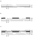
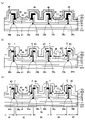
- FIG. 2A is a cross-sectional view of a substrate after film formation in a first film formation unit; It is sectional drawing of the board
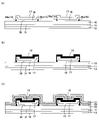
- FIG. 3C is an explanatory view of the manufacturing process of the solar cell panel following FIG.
- FIG. 4C is an explanatory view of the manufacturing process of the solar cell panel following FIG. 4C
- FIG. 2C is a cross-sectional view of the substrate after forming an electrode resist layer in the 2-resist layer forming section
- (c) is a cross-sectional view of the substrate after film formation in the transparent electrode layer forming section.
- FIG. 5C is an explanatory view of the manufacturing process of the solar cell panel following FIG.
- FIG. 4 is a cross-sectional view of the substrate after peeling off the resist layer for the substrate;
- the resist layer is indicated by black coating, and the remaining layers are omitted from hatching.
- FIG. 2 is an explanatory diagram of a solar cell panel according to a second embodiment of the present invention, where (a) is a cross-sectional view showing the relationship between a photoelectric conversion substrate and an electrode layer, and (b) is a detailed view of the photoelectric conversion substrate of (a); It is a sectional view showing. In both (a) and (b), the insulating layer derived from the resist layer is shown in black for easy understanding, and the hatching of the rest is omitted. It is a block diagram conceptually showing a semiconductor manufacturing apparatus used in a second embodiment of the present invention. 8 is an explanatory view of the manufacturing process of the solar cell panel of FIG.
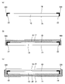
- FIG. 7 is a cross-sectional view of the substrate after forming the resist layer in the resist layer forming section, and (b) is a film forming in the second film forming section.
- FIG. 10C is a cross-sectional view of the substrate after the film formation, and FIG. In order to facilitate understanding, only the layers formed in each step are indicated by hatching, the resist layer is indicated by black coating, and the remaining layers are omitted from hatching.
- FIG. 9C is an explanatory view of the manufacturing process of the solar cell panel following FIG. 9C, (a) is a cross-sectional view of the substrate after film formation in the transparent electrode layer forming part, and (b) is a metal electrode layer forming part.
- FIG. 3C is a cross-sectional view of the substrate after forming a film in
- (c) is a cross-sectional view of the substrate after the resist layer is peeled off at the mechanical peeling unit.
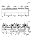
- FIG. 3 is an explanatory diagram of a solar cell panel according to a third embodiment of the present invention, where (a) is a cross-sectional view showing the relationship between a photoelectric conversion substrate and an electrode layer, and (b) is a detailed view of the photoelectric conversion substrate of (a); It is a sectional view showing.
- FIG. 12 is an explanatory view of the manufacturing process of the solar cell panel of FIG. 11, (a) is a cross-sectional view of the substrate after forming the first resist layer in the first film forming section, and (b) is a second film forming section.
- FIG. 13C is an explanatory view of the manufacturing process of the solar cell panel following FIG.
- FIG. 8C is a cross-sectional view of the substrate after forming two resist layers, and FIG.
- FIG. 7C is a cross-sectional view of the substrate after forming a second intrinsic semiconductor layer and a second conductivity type semiconductor layer in a second film forming section;
- the resist layer is indicated by black, and the remaining layers are omitted from hatching.
- FIG. 14C is an explanatory view of the manufacturing process of the solar cell panel following FIG. 14C
- FIG. FIG. 4C is a cross-sectional view of the substrate after forming the electrode resist layer in the film forming unit
- FIG. is a cross-sectional view of.
- the resist layer is indicated by black, and the remaining layers are omitted from hatching.
- FIG. 15C is an explanatory view of the manufacturing process of the solar cell panel following FIG.
- FIG. 4C is a cross-sectional view of the substrate after the electrode resist layer is peeled off in the peeling unit, and FIG. In order to facilitate understanding, only the layers formed immediately before are indicated by hatching, the resist layer is indicated by black, and the remaining layers are omitted from hatching.
- FIG. 4 is a cross-sectional view of a solar cell panel according to another embodiment of the invention.
- a solar cell panel 1 according to the first embodiment of the present invention has a back panel in which a first electrode layer 3 and a second electrode layer 5 are formed on the back main surface 57 side of a photoelectric conversion substrate 2, as shown in FIG. 1(a). It is a contact type solar cell panel.
- the solar cell panel 1 is provided with a first electrode layer 3 and a second electrode layer 5 adjacent to each other, and includes short-circuit prevention grooves 7 and 8 at the boundaries between the first electrode layer 3 and the second electrode layer 5. ing.
- the photoelectric conversion substrate 2 is a photoelectric conversion unit that has a PN junction and converts light energy into electrical energy. As shown in FIG. 1B, the photoelectric conversion substrate 2 includes semiconductor layers 16, 20, 17, and 21 on the first main surface 30 side of the semiconductor substrate 10, and receives light on the second main surface 31 side of the semiconductor substrate 10. It is a multi-layer substrate having a side semiconductor layer 11 and an antireflection layer 12 .
- the photoelectric conversion substrate 2 includes a first region 35 having a cross-sectional structure in which a first intrinsic semiconductor layer 16 and a first conductivity type semiconductor layer 17 are stacked in this order on a first main surface 30 of a semiconductor substrate 10; and a second region 36 having a cross-sectional structure in which the second intrinsic semiconductor layer 20 and the second conductivity type semiconductor layer 21 are stacked in this order on the first main surface 30 of the .
- the photoelectric conversion substrate 2 includes boundary insulating layers 38 a and 38 b at the boundary between the first region 35 and the second region 36 .
- the photoelectric conversion substrate 2 has a light receiving side semiconductor layer 11 and an antireflection layer 12 in this order on the second main surface 31 , and the antireflection layer 12 constitutes the light receiving side main surface 56 of the solar cell panel 1 . .
- the semiconductor substrate 10 is an n-type or p-type semiconductor substrate, and more specifically, an n-type or p-type crystalline silicon substrate.
- a single crystal silicon substrate or a polycrystalline silicon substrate can be used as the semiconductor substrate 10 .
- the semiconductor substrate 10 preferably has a pyramid-shaped texture structure formed on the surface of the first principal surface 30 and/or the second principal surface 31 .
- the first intrinsic semiconductor layer 16 is a silicon thin film that does not substantially contain dopants, and preferably has a dopant concentration of 1/100 or less of the dopant concentration of the first conductivity type semiconductor layer 17 .
- the first conductivity type semiconductor layer 17 is an n-type or p-type silicon-based thin film layer containing a dopant, and is a p-type silicon layer in this embodiment.
- the second intrinsic semiconductor layer 20 is a silicon thin film that does not substantially contain dopants, and preferably has a dopant concentration of 1/100 or less of the dopant concentration of the second conductivity type semiconductor layer 21 .
- the second-conductivity-type semiconductor layer 21 is a silicon layer containing a dopant and having a conductivity type opposite to that of the first-conductivity-type semiconductor layer 17 . That is, when the conductivity type of the first conductivity type semiconductor layer 17 is n-type, the conductivity type of the second conductivity type semiconductor layer 21 is p-type, and when the conductivity type of the first conductivity type semiconductor layer 17 is p-type, , the conductivity type of the second conductivity type semiconductor layer 21 is n-type. As described above, in this embodiment, the first conductivity type semiconductor layer 17 is a p-type silicon layer, so the second conductivity type semiconductor layer 21 is formed of an n-type semiconductor layer.
- the boundary-side insulating layers 38a and 38b are layers having insulating properties derived from resist layers 15 and 18, which will be described later.
- the boundary-side insulating layers 38 a and 38 b are provided between the interface between the intrinsic semiconductor layers 16 and 20 and the interface between the conductive semiconductor layers 17 and 21 .
- the boundary-side insulating layer 38b extends outward from the semiconductor substrate 10 (toward the electrode layers 3 and 5).
- the boundary-side insulating layer 38 a has a peeling strength of 1 N or less with respect to the semiconductor substrate 10 and can be mechanically peeled off from the semiconductor substrate 10 .
- the boundary-side insulating layer 38 b has a peeling strength of 1 N or less with respect to the first-conductivity-type semiconductor layer 17 and can be mechanically peeled off from the first-conductivity-type semiconductor layer 17 .
- the light receiving side semiconductor layer 11 is an intrinsic silicon thin film that does not substantially contain dopants.
- the antireflection layer 12 is a low-reflection layer that has translucency and suppresses reflection of light.
- the antireflection layer 12 can be formed of, for example, metal oxides such as silicon oxide, zinc oxide, and titanium oxide, and metal nitrides such as silicon nitride.
- the antireflection layer 12 is preferably made of silicon nitride from the viewpoint of the optical confinement effect of incident light.
- the first electrode layer 3 is an electrode that forms a pair with the second electrode layer 5 and extracts electrical energy photoelectrically converted by the photoelectric conversion substrate 2 together with the second electrode layer 5 .
- the first electrode layer 3 is formed on the first conductivity type semiconductor layer 17 in the first region 35 as shown in FIG. It is formed on the mold semiconductor layer 21 .
- the electrode layers 3 and 5 are composed of a transparent electrode layer 23 and a metal electrode layer 25, respectively, as shown in FIG. 1(a).
- the transparent electrode layer 23 is a transparent conductive layer having transparency and conductivity.
- the transparent electrode layer 23 is made of a transparent conductive oxide such as indium tin oxide (ITO) or tungsten-doped indium oxide (IWO). It is a conductive oxide layer. IWO is used for the transparent electrode layer 23 of this embodiment.
- the metal electrode layer 25 is a conductive layer having higher conductivity than the transparent electrode layer 23, and can be made of, for example, metals such as gold, silver, copper, platinum, aluminum, nickel, palladium, or alloys containing these metals.
- the short-circuit preventing grooves 7 and 8 are grooves for preventing short-circuiting due to contact between the first electrode layer 3 and the second electrode layer 5, as shown in FIG. 1(a). As shown in FIG. 1B, the short-circuit prevention grooves 7 and 8 are provided across the first conductivity type semiconductor layer 17 and the second conductivity type semiconductor layer 21 and have the first conductivity type semiconductor layer 17 as the bottom. is. The short-circuit prevention grooves 7 and 8 extend along the boundary between the first conductivity type semiconductor layer 17 and the second conductivity type semiconductor layer 21 . A part of the inner walls of the short-circuit prevention grooves 7 and 8 is formed of the groove-side insulating layer 40 .
- the groove-side insulating layer 40 extends from the first-conductivity-type semiconductor layer 17 toward the base end side (opening side) in the depth direction of the short-circuit prevention grooves 7 and 8, and the tip portion is the transparent electrode. It is positioned inside the layer 23 .
- the groove-side insulating layer 40 is a layer having insulating properties derived from the electrode resist layer 22 to be described later.
- the groove-side insulating layer 40 has a peeling strength of 1 N or less with respect to the first conductivity type semiconductor layer 17 and can be mechanically peeled off from the conductivity type semiconductor layer 17 .
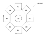
- the manufacturing apparatus 201 is a semiconductor manufacturing apparatus having a cluster structure as shown in FIG.
- the first cluster section 202 includes a first transfer section 210 as a center, a loading section 211 , a first film forming section 212 , a second film forming section 213 , a third film forming section 214 , and a first connecting section 218 .
- the first temporary placement portion 217, the first mechanical peeling portion 216, and the first resist layer forming portion 215 are arranged in the circumferential direction.
- the first transfer section 210 includes a loading section 211, film forming sections 212 to 214, a first connecting section 218, a first temporary placement section 217, a first mechanical peeling section 216, and a first resist layer forming section 215.
- the loading section 211 is a section for loading the semiconductor substrate 10 into the first cluster section 202 from the outside.
- the first film forming section 212 is provided with a plasma CVD apparatus, and is a section for forming the light-receiving side semiconductor layer 11 and the antireflection layer 12 .
- the second film forming section 213 is equipped with a plasma CVD apparatus, and is a section for forming the first intrinsic semiconductor layer 16 and the first conductivity type semiconductor layer 17 .
- the third film forming section 214 is equipped with a plasma CVD apparatus and is a section for forming the second intrinsic semiconductor layer 20 and the second conductivity type semiconductor layer 21 .
- the first resist layer forming unit 215 is provided with a coating device capable of coating a semiconductor resist material that can be mechanically stripped, and is a portion for forming the resist layers 15 and 18 with a predetermined pattern.
- the first resist layer forming unit 215 includes a printing device capable of applying a resist material in a predetermined pattern, an ultraviolet irradiation device capable of irradiating the applied resist material with ultraviolet rays, and a heating device for heating the applied resist material. have equipment.
- the first mechanical stripping unit 216 is a mechanical stripping unit that includes a mechanical stripping device and mechanically strips the resist layers 15 and 18 from the substrate.
- the first temporary placement section 217 is a section for temporarily placing the base material transferred by the first transfer section 210, and is capable of receiving the substrate when downstream processes are delayed.
- the first connecting part 218 is a part that is connected to the second cluster part 203 and carries out the substrate on which the film has been formed from the first cluster part 202 to the second cluster part 203 .
- the second cluster part 203 has a second transfer part 220 as a center, a second connecting part 221, a second resist layer forming part 222, a transparent electrode layer forming part 223, and a metal electrode layer forming part.
- the portion 224, the unloading portion 227, the second temporary placement portion 226, and the second mechanical peeling portion 225 are arranged in the circumferential direction.
- the second connecting part 221 is connected to the first connecting part 218 of the first cluster part 202 and is a part for loading the substrate unloaded from the first cluster part 202 into the second cluster part 203 .
- the second resist layer forming section 222 is provided with a coating device capable of coating an electrode resist material that can be mechanically stripped, and is a section for forming the electrode resist layer 22 of a predetermined pattern.
- the second resist layer forming unit 222 includes a printing device capable of applying a resist material in a predetermined pattern, an ultraviolet irradiation device capable of irradiating the applied resist material with ultraviolet rays, and a heating device for heating the applied resist material. have equipment.
- the transparent electrode layer forming unit 223 is a film forming unit that has a sputtering device and forms the transparent electrode layer 23 .
- the metal electrode layer forming unit 224 is a metal electrode layer forming unit that has a vacuum deposition device and forms the metal electrode layer 25 .
- the second mechanical stripping unit 225 is a mechanical stripping unit that includes a mechanical stripping device and mechanically strips the electrode resist layer 22 from the substrate.
- the second temporary placement section 226 is a section for temporarily placing the substrates transferred by the second transfer section 220, and is capable of receiving the substrates when downstream processes are delayed.
- the unloading section 227 is a section for unloading the solar cell panel 1 after film formation from the second cluster section 203 to the outside.
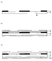
- the semiconductor substrate 10 is loaded from the loading section 211 of the first cluster section 202 and transferred to the first film forming section 212 by the first transfer section 210 . Then, as shown in FIG. 3A, the light-receiving-side semiconductor layer 11 is formed on the second main surface 31 of the semiconductor substrate 10 in the first film forming section 212 (light-receiving-side semiconductor layer forming step), and further, the light-receiving-side semiconductor layer An antireflection layer 12 is formed on the layer 11 (antireflection layer forming step).
- a first resist layer 15 (second semiconductor resist layer) having a predetermined pattern is formed on the first main surface 30 of the semiconductor substrate 10 in the first resist layer forming section 215 (first resist layer forming step, first 2 semiconductor resist layer formation step).
- the first resist layer 15 formed at this time has heat resistance and can maintain its shape when the semiconductor layers 16 and 17 are formed.
- the first resist layer 15 is a resist layer that can be mechanically peeled off, and can be peeled off from the semiconductor substrate 10 when an external force is applied.
- the first resist layer 15 is preferably a resist layer having a peel strength of 1N or less with respect to the semiconductor substrate 10 .
- the first resist layer 15 may form an overhanging portion that overhangs other portions in the surface direction of the semiconductor substrate 10 as necessary.
- An ultraviolet curable resin and/or a thermosetting resin is used as the resist material forming the first resist layer 15 of the present embodiment. 1 resist layer 15 is formed.
- the substrate on which the first resist layer 15 is formed is transferred from the first resist layer forming unit 215 to the second film forming unit 213 by the first transfer unit 210, and then, as shown in FIG.
- a first intrinsic semiconductor layer 16 is formed over the semiconductor substrate 10 and the first resist layer 15 in the film portion 213 (first intrinsic semiconductor layer forming step), and a first conductive film is formed on the first intrinsic semiconductor layer 16 .
- type semiconductor layer 17 (first conductivity type semiconductor layer forming step).
- the substrate on which the semiconductor layers 16 and 17 are formed is transferred from the second film forming section 213 to the first mechanical peeling section 216 by the first transfer section 210, and as shown in FIG.
- the first resist layer 15 is mechanically peeled off from the semiconductor substrate 10 at a portion 216, and the first intrinsic semiconductor layer 16, which is positioned outside the first resist layer 15 with respect to the semiconductor substrate 10 and is based on the first resist layer 15, is formed.
- a part of the semiconductor layer 17 and a part of the first conductivity type semiconductor layer 17 are peeled off and removed (first removing step, second peeling step).
- the first resist layer 15 is peeled off from the semiconductor substrate 10 by the first mechanical peeling section 216, and a part of the first intrinsic semiconductor layer 16 on the first resist layer 15 and the first conductivity type semiconductor layer 17 are removed. peel off some.
- the first resist layer 15 is not completely removed, and part of the residue remains between the first intrinsic semiconductor layer 16 and the semiconductor substrate 10, leaving the boundary side insulating layer 38a. It is formed. That is, the first intrinsic semiconductor layer 16 is partially covered with the first resist layer 15 on the end face. Further, when the first resist layer 15 is formed with overhangs, it is preferable to mechanically remove the first resist layer 15 from the overhangs exposed from the semiconductor layers 16 and 17 by rolling over the first resist layer 15 . By doing so, the semiconductor layers 16 and 17 are less likely to be damaged during mechanical peeling.
- the substrate from which the first resist layer 15 has been removed is transferred from the first mechanical stripping unit 216 to the first resist layer forming unit 215 by the first transfer unit 210, and the first resist layer 15 is removed as shown in FIG.
- the second resist layer 18 (first semiconductor resist layer) is formed on the first conductivity type semiconductor layer 17 remaining after the removal of the first resist layer 15 (second resist layer forming step, first semiconductor resist layer forming step).
- the second resist layer 18 formed at this time has heat resistance and can maintain its shape when the semiconductor layers 20 and 21 are formed.
- the second resist layer 18 is a resist layer that can be mechanically peeled off, and can be peeled off from the first conductivity type semiconductor layer 17 when an external force is applied.
- the second resist layer 18 is preferably a resist layer having a peel strength of 1N or less with respect to the first conductivity type semiconductor layer 17 .
- the second resist layer 18 is formed so as to protrude from the first conductivity type semiconductor layer 17 and straddle the semiconductor substrate 10 .
- the second resist layer 18 covers the first conductivity type semiconductor layer 17 from the top to the side surface (end surface), and furthermore, the first resist layer 15, the first intrinsic semiconductor layer 16, and the first conductivity type semiconductor layer 17 are covered. It covers the sides (end faces). Thus, the first intrinsic semiconductor layer 16 and the first conductivity type semiconductor layer 17 are protected by the second resist layer 18 . Moreover, the second resist layer 18 may form an overhanging portion that overhangs other portions in the surface direction of the semiconductor substrate 10 as necessary. An ultraviolet curable resin and/or a thermosetting resin is used as the resist material that constitutes the second resist layer 18 of the present embodiment. 2 A resist layer 18 is formed.
- the substrate on which the second resist layer 18 is formed is transferred from the first resist layer forming unit 215 to the third film forming unit 214 by the first transfer unit 210, and the third film forming unit 214 is transferred as shown in FIG.
- the second intrinsic semiconductor layer 20 is formed over the semiconductor substrate 10 and the second resist layer 18 (second intrinsic semiconductor layer forming step), and a second conductivity type semiconductor is formed on the second intrinsic semiconductor layer 20 .
- a layer 21 is formed (second conductivity type semiconductor layer forming step).
- the first intrinsic semiconductor layer 16 and the first conductivity type semiconductor layer 17 are covered with the second resist layer 18 , they do not contact the second intrinsic semiconductor layer 20 and the second conductivity type semiconductor layer 21 . Moreover, when the overhanging portion is formed in the second resist layer 18 , it is preferable to expose the overhanging portion of the second resist layer 18 from the semiconductor layers 20 and 21 .
- the substrate on which the semiconductor layers 20 and 21 are formed is transferred from the third film forming section 214 to the first mechanical peeling section 216 by the first transfer section 210, and the first mechanical peeling section 216 is transferred as shown in FIG.
- the second resist layer 18 is mechanically stripped from the first conductivity type semiconductor layer 17, and a second intrinsic semiconductor is positioned outside the second resist layer 18 with respect to the semiconductor substrate 10, and the second resist layer 18 serves as a base.
- a portion of the layer 20 and a portion of the second conductivity type semiconductor layer 21 are peeled off to form the photoelectric conversion substrate 2 (second removal step, first peeling step).
- the second resist layer 18 is peeled off from the first conductivity type semiconductor layer 17 by the first mechanical peeling section 216 to remove a portion of the second intrinsic semiconductor layer 20 on the second resist layer 18 and the second conductivity type semiconductor layer 17 .
- a portion of the semiconductor layer 21 is peeled off.
- a boundary side insulating layer 38b is formed remaining at the interface between the layer 17 and the second conductivity type semiconductor layer 21 . That is, at the interface between the first intrinsic semiconductor layer 16 and the second intrinsic semiconductor layer 20 and at the interface between the first conductivity type semiconductor layer 17 and the second conductivity type semiconductor layer 21, boundaries formed of the resist layers 15 and 18 are provided. Side insulating layers 38a and 38b are located, and the first conductivity type semiconductor layer 17 and the second conductivity type semiconductor layer 21 are electrically insulated by the boundary side insulating layers 38a and 38b.
- the second resist layer 18 has overhangs
- the photoelectric conversion substrate 2 is transferred from the first mechanical peeling portion 216 to the first connection portion 218 by the first transfer portion 210 , and then transferred from the first connection portion 218 of the first cluster portion 202 to the second transfer portion of the second cluster portion 203 .
- the photoelectric conversion substrate 2 is transferred to the connecting portion 221 .
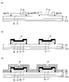
- the photoelectric conversion substrate 2 When the photoelectric conversion substrate 2 is transferred to the second connection portion 221 , the photoelectric conversion substrate 2 is transferred from the second connection portion 221 to the second resist layer forming portion 222 by the second transfer portion 220 . Then, as shown in FIG. 5B, in the second resist layer forming portion 222, the first conductivity type semiconductor layer 17 is formed at the boundary portion between the first conductivity type semiconductor layer 17 and the second conductivity type semiconductor layer 21 of the photoelectric conversion substrate 2. , and the electrode resist layer 22 is formed across the second conductivity type semiconductor layer 21 (electrode resist layer forming step).
- the electrode resist layer 22 formed at this time is a resist layer that has heat resistance and can be mechanically peeled off, and is peeled off when an external force is applied.
- the electrode resist layer 22 is a resist layer having a peeling strength of 1N or less with respect to the photoelectric conversion substrate 2. Specifically, the peeling strength with respect to each of the first conductivity type semiconductor layer 17 and the second conductivity type semiconductor layer 21 is 1N. The following are preferable.
- the electrode resist layer 22 covers the end faces of the second intrinsic semiconductor layer 20 and the second conductivity type semiconductor layer 21 . In addition, the electrode resist layer 22 may form an overhanging portion that overhangs other portions in the surface direction of the semiconductor substrate 10 as necessary.
- An ultraviolet curable resin and/or a thermosetting resin is used as the resist material forming the electrode resist layer 22 of the present embodiment.
- a resist layer 22 is formed.
- the substrate on which the electrode resist layer 22 is formed is transferred from the second resist layer forming unit 222 to the transparent electrode layer forming unit 223 by the second transfer unit 220, and the transparent electrode layer is formed as shown in FIG. 5(c).
- the transparent electrode layer 23 is formed across the first conductivity type semiconductor layer 17, the electrode resist layer 22, and the second conductivity type semiconductor layer 21 (transparent electrode layer forming step).
- the electrode resist layer 22 has a projecting portion, it is preferable to expose the projecting portion of the electrode resist layer 22 from the transparent electrode layer 23 .
- the substrate on which the transparent electrode layer 23 is formed is transferred from the transparent electrode layer forming unit 223 to the metal electrode layer forming unit 224 by the second transfer unit 220, and as shown in FIG. to form a metal electrode layer 25 (metal electrode layer forming step).
- the electrode resist layer 22 has a projecting portion, it is preferable to expose the projecting portion of the electrode resist layer 22 from the metal electrode layer 25 .
- the substrate on which the metal electrode layer 25 is formed is transferred from the metal electrode layer forming part 224 to the second mechanical peeling part 225 by the second transfer part 220, and as shown in FIG.
- the electrode resist layer 22 is mechanically peeled off from the substrate, and a portion of the transparent electrode layer 23 located outside the electrode resist layer 22 with respect to the semiconductor substrate 10 and underlying the electrode resist layer 22 and the metal electrode are removed. A part of the layer 25 is stripped and removed (electrode stripping step).
- the electrode resist layer 22 is peeled off from the substrate by the second mechanical peeling unit 225 to peel off a portion of the transparent electrode layer 23 and a portion of the metal electrode layer 25 on the electrode resist layer 22 .
- the short-circuit preventing grooves 7 and 8 are formed by stripping the electrode resist layer 22 .
- the transparent electrode layer 23 and the metal electrode layer 25 are divided into a plurality of portions by the short-circuit prevention grooves 7 and 8 to be partitioned into a first region 35 and a second region 36, thereby forming the first electrode layer 3 and the second electrode layer 5. be done.
- the electrode resist layer 22 is not completely peeled off, and part of the residue remains inside the transparent electrode layer 23 to form the groove-side insulating layer 40. compose the department.
- the groove-side insulating layer 40 constitutes inner walls from the bottom formed of the first-conductivity-type semiconductor layer 17 to the electrode layers 3 and 5 .
- the overhanging portions are formed in the electrode resist layer 22
- the overhanging portions exposed from the electrode layers 23 and 25 are preferably peeled off mechanically by rolling over the electrode resist layer 22. As shown in FIG. By doing so, the electrode layers 23 and 25 are less likely to be damaged during mechanical peeling.
- the substrate from which the electrode resist layer 22 has been removed is transferred from the second mechanical stripping section 225 to the carrying-out section 227 by the second transfer section 220 and discharged from the carrying-out section 227 to the outside of the second cluster section 203 .
- wiring members such as interconnectors are attached to the electrode layers 3 and 5 as necessary to complete the solar cell panel 1 .
- the electrode resist layer 22 is peeled off, the transparent electrode layer 23 and the metal electrode layer 25 are partly peeled off, and the transparent electrode layer 23 and the metal electrode layer 25 are patterned.
- the transparent electrode layer 23 and the metal electrode layer 25 can be patterned without using an etchant.
- the transparent electrode layer 23 is not patterned by dissolving the transparent electrode layer 23, the transparent electrode containing tungsten-doped indium oxide, which is difficult to dissolve in the etchant, is formed. Even layer 23 can be patterned.
- the resist layers 15 and 18 are peeled off to partially peel off the semiconductor layers 16, 17, 20 and 21, and the semiconductor layers 16, 17, 20 and 21 are patterned.
- the semiconductor layers 16, 17, 20 and 21 can be patterned without using an etchant.
- the short circuit prevention grooves 7 and 8 are formed in the boundary portion between the first electrode layer 3 and the second electrode layer 5, the electrode layers 3 and 5 are in contact with each other. short circuit can be prevented.
- the boundary side insulating layers 38a and 38b cover the end faces of the first conductivity type semiconductor layer 17, and the groove side insulating layer 40 covers the end faces of the second conductivity type semiconductor layer 21. covering. Therefore, it is possible to prevent the end face of the first conductivity type semiconductor layer 17 from contacting the second conductivity type semiconductor layer 21 and the end face of the second conductivity type semiconductor layer 21 from contacting the first conductivity type semiconductor layer 17.
- the electrode resist layer 22 can be easily peeled off.
- a first electrode layer 303 is formed on a light-receiving side main surface 306 of a photoelectric conversion substrate 302, and a second electrode layer 305 is formed on a back side main surface 307. It is a double-sided electrode type solar cell panel.
- the photoelectric conversion substrate 302 has a first intrinsic semiconductor layer 16 and a first conductivity type semiconductor layer 17 laminated in this order on the first main surface 30 side of the semiconductor substrate 10, and a second A second intrinsic semiconductor layer 20 and a second conductivity type semiconductor layer 21 are laminated in this order on the main surface 31 side.
- the first electrode layer 303 is an electrode layer provided on the light-receiving-side main surface 306 side with respect to the photoelectric conversion substrate 302, and is composed of a transparent electrode layer 23a and a metal electrode layer 25a.
- the second electrode layer 305 is an electrode layer provided on the back main surface 307 side with respect to the photoelectric conversion substrate 302, and is composed of a transparent electrode layer 23b and a metal electrode layer 25b.
- the solar cell panel 301 has transparent electrode layers 23 a and 23 b covering the entire main surfaces 306 and 307 of the photoelectric conversion substrate 302 , and the transparent electrode layers 23 a and 23 b covering the photoelectric conversion substrate 302 . end faces 308 and 309 of the . Specifically, the end surfaces 308 and 309 of the photoelectric conversion substrate 302 are covered with the first transparent electrode layer 23a, and are covered with the second transparent electrode layer 23b from the outside of the first transparent electrode layer 23a. In the solar cell panel 301, an insulating layer 310 is interposed between the end faces 308, 309 of the photoelectric conversion substrate 302 and the inner transparent electrode layer 23a.
- the insulating layer 310 is a layer having insulating properties derived from the electrode resist layer 22, has a peeling strength to the photoelectric conversion substrate 302 of 1 N or less, and can be mechanically peeled from the photoelectric conversion substrate 302.
- the solar cell panel 301 has short-circuit prevention grooves 337 and 338 extending along the end faces 308 and 309 as shown in FIG. 7(b).
- the short-circuit prevention grooves 337 and 338 are grooves that prevent short-circuiting between the first electrode layer 303 and the second electrode layer 305 .
- the short-circuit preventing grooves 337 and 338 are grooves having a depth from at least the first transparent electrode layer 23a to the first intrinsic semiconductor layer 16, and are grooves having the semiconductor substrate 10 as the bottom in this embodiment.
- a manufacturing apparatus 401 is a semiconductor device having a cluster structure and includes a cluster section 402 as shown in FIG.
- the cluster section 402 includes a first transfer section 210 as a center, a loading section 211, a second film forming section 213, a third film forming section 214, a transparent electrode layer forming section 223, an unloading section 227, and a metal electrode.
- the layer forming portion 424, the second mechanical peeling portion 225, and the second resist layer forming portion 222 are arranged in the circumferential direction.
- the metal electrode layer forming unit 424 is a film forming unit that includes a printing device and forms the metal electrode layer 25 using a conductive paste.
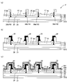
- the semiconductor substrate 10 is carried into the cluster section 402 from the carrying-in section 211, transferred to the resist layer forming section 222 by the first transfer section 210, and transferred to the resist layer forming section 222 as shown in FIG. , a resist layer 22 having a predetermined pattern is formed on the first main surface 30 of the semiconductor substrate 10 (resist layer forming step).
- the resist layer 22 is provided at the end of the semiconductor substrate 10 and extends along the end surfaces 308 and 309 . Moreover, the resist layer 22 is provided over a portion of the first main surface 30 of the semiconductor substrate 10 and the end surfaces 308 and 309 .
- the substrate on which the resist layer 22 is formed is transferred from the resist layer forming unit 222 to the second film forming unit 213 by the first transfer unit 210, and the semiconductor is transferred to the second film forming unit 213 as shown in FIG. 9B.
- a first intrinsic semiconductor layer 16 is formed over the resist layer 22 from a portion exposed from the resist layer 22 on the substrate 10 (first intrinsic semiconductor layer forming step).
- a conductive semiconductor layer 17 is deposited (first conductive semiconductor layer forming step).
- the first intrinsic semiconductor layer 16 is formed entirely on the side of the first main surface 30 , wraps around to the end faces 308 and 309 , and is also formed on the resist layer 22 at the end faces 308 and 309 .
- the first conductivity type semiconductor layer 17 is formed entirely on the first intrinsic semiconductor layer 16 , wraps around the end faces 308 and 309 , and is also formed on the first intrinsic semiconductor layer 16 on the end faces 308 and 309 side.
- the substrate on which the semiconductor layers 16 and 17 are formed is transferred from the second film forming unit 213 to the third film forming unit 214 by the first transfer unit 210, and then transferred to the third film forming unit 214 as shown in FIG. 9(c).
- the second intrinsic semiconductor layer 20 is formed on the second main surface 31 of the semiconductor substrate 10 (second intrinsic semiconductor layer forming step), and the second conductivity type semiconductor layer 21 is formed on the second intrinsic semiconductor layer 20 . (second conductivity type semiconductor layer forming step).
- the second intrinsic semiconductor layer 20 is formed on the entire second main surface 31 side, wraps around to the end faces 308 and 309, and is formed on the first conductivity type semiconductor layer 17 also on the end faces 308 and 309 side.
- the second conductivity type semiconductor layer 21 is formed entirely on the second intrinsic semiconductor layer 20 , wraps around the end faces 308 and 309 , and is also formed on the second intrinsic semiconductor layer 20 on the end faces 308 and 309 side. That is, the second intrinsic semiconductor layer 20 is interposed between the first conductivity type semiconductor layer 17 and the second conductivity type semiconductor layer 21 .
- the substrate on which the semiconductor layers 20 and 21 are formed is transferred from the third film forming section 214 to the transparent electrode layer forming section 223 by the first transfer section 210, and the substrate is transferred to the transparent electrode layer forming section as shown in FIG. 10(a).
- transparent electrode layers 23a and 23b are formed on both sides of the substrate (transparent electrode layer forming step). That is, the transparent electrode layer 23 a is formed on the semiconductor layer 17 of the first conductivity type, and the transparent electrode layer 23 b is formed on the semiconductor layer 21 of the second conductivity type.
- the first transparent electrode layer 23a is formed entirely on the first conductivity type semiconductor layer 17, wraps around the end faces 308 and 309, and is formed on the second conductivity type semiconductor layer 21 on the end faces 308 and 309 side.
- the second transparent electrode layer 23b is formed entirely on the second conductivity type semiconductor layer 21, wraps around the end faces 308 and 309, and is formed on the first transparent electrode layer 23a on the end faces 308 and 309 side. That is, the transparent electrode layers 23a and 23b are electrically connected on the end surfaces 308 and 309 side.
- the substrate on which the transparent electrode layers 23a and 23b are formed is transferred from the transparent electrode layer forming unit 223 to the metal electrode layer forming unit 424 by the first transfer unit 210, and the metal electrode layers are formed as shown in FIG. 10(b).
- Metal electrode layers 25a and 25b are formed on the transparent electrode layers 23a and 23b in a portion 424 (metal electrode layer forming step).
- the first metal electrode layer 25a is formed in a comb-like pattern, and constitutes busbar electrode portions extending in a predetermined direction and finger electrode portions extending in a direction orthogonal to the busbar electrode portions.
- the second metal electrode layer 25b is formed in a comb-like pattern, and constitutes busbar electrode portions extending in a predetermined direction and finger electrode portions extending in a direction orthogonal to the busbar electrode portions.
- the substrate on which the metal electrode layers 25a and 25b are formed is transferred from the metal electrode layer forming part 424 to the second mechanical peeling part 225 by the first transfer part 210, and the second mechanical peeling is performed as shown in FIG. 10(c).
- the electrode resist layer 22 is mechanically stripped from the substrate (electrode stripping step).
- the electrode resist layer 22 is mechanically peeled off, so that one of the semiconductor layers 16 and 17 located outside the electrode resist layer 22 with respect to the semiconductor substrate 10 and on which the electrode resist layer 22 serves as a base. A portion of the first transparent electrode layer 23a is peeled off and removed to form short-circuit prevention grooves 337 and 338. As shown in FIG. At this time, on the end surfaces 308 and 309, the electrode resist layer 22 is not peeled off, and a part of the residue remains inside the transparent electrode layer 23a to form the insulating layer 310. Form part of the inner wall.
- the substrate from which the electrode resist layer 22 has been removed is transferred from the second mechanical stripping section 225 to the carry-out section 227 by the first transfer section 210 and discharged from the carry-out section 227 to the outside of the cluster section 402 .
- wiring members such as interconnectors are attached to the electrode layers 303 and 305 to complete the solar cell panel 301 .
- the insulating layer 310 is interposed between the end surfaces 308 and 309 of the semiconductor substrate 10 and the transparent electrode layer 23a of the first electrode layer 303, and the semiconductor substrate 10 serves as the bottom portion.
- Short-circuit preventing grooves 337 and 338 extend along the end surfaces 308 and 309 of the semiconductor substrate 10 . Therefore, a short circuit between the first electrode layer 303 and the second electrode layer 305 can be prevented.
- a solar cell panel 501 according to the third embodiment of the present invention has a first electrode layer 503 and a second electrode layer 505 formed on the back main surface 57 side of a photoelectric conversion substrate 502, as shown in FIG. 11(a). is.
- the photoelectric conversion substrate 502 includes semiconductor layers 16, 20, 17, and 21 on the first main surface 30 side of the semiconductor substrate 10, and receives light on the second main surface 31 side of the semiconductor substrate 10. It has a side semiconductor layer 11 , a transparent conductive layer 510 and a light incident layer 511 .
- the transparent conductive layer 510 is a layer having transparency and conductivity.
- the transparent conductive layer 510 is made of a transparent conductive oxide such as indium tin oxide (ITO) or tungsten-doped indium oxide (IWO). It is an oxide layer.
- the sheet resistance of the transparent conductive layer 510 is preferably 100 ⁇ /sq or more and 300 ⁇ /sq or less.
- the light incident layer 511 has insulating properties and is formed of a resin material such as an ultraviolet curable resin and/or a thermosetting resin that is cured by being irradiated with ultraviolet rays and/or heated.
- the light incident layer 511 is made of a resin material such as acrylic resin (with a refractive index of 1.4 to 1.5) or a high-transmitting material having a refractive index of 1.7 to 1.7 to 1.7 to 1.7 from the viewpoint of adjusting the refractive index, appearance, and insulating properties. It is preferred to use a high refractive index material of 0.9.
- the electrode layers 503 and 505 are composed of a transparent electrode layer 23, an underlying electrode layer 520, and a metal electrode layer 521, respectively, as shown in FIG. 11(a).
- the base electrode layer 520 is a layer that serves as a base for the metal electrode layer 521, and is a layer that constitutes a seed layer when the metal electrode layer 521 is formed.
- the base electrode layer 520 is a conductive layer having conductivity, and specifically, titanium nitride (TiN) or the like can be used.
- the metal electrode layer 521 is a plated layer formed by a plating method, and is a layer having more conductivity than the transparent electrode layer 23 .
- the same material as the metal electrode layer 25 of the first embodiment can be used as long as it can be formed by plating.
- the metal electrode layer 521 may be formed by an electrolytic plating method, or may be formed by an electroless plating method.
- a manufacturing apparatus 601 is a semiconductor device having a cluster structure and includes a cluster section 602 as shown in FIG.
- the cluster unit 602 includes a transfer unit 210 as a center, a loading unit 211, a first film forming unit 603, a second film forming unit 605, a third film forming unit 606, a mechanical peeling unit 216, and a fourth film forming unit 606.
- the film portion 607, the temporary placement portion 217, and the unloading portion 227 are arranged in the circumferential direction.
- the first film forming section 603 is a section for forming the resist layers 15 , 18 , 22 and the light incident layer 511 .
- the first film forming unit 603 includes a printing device capable of applying a resist material constituting each of the resist layers 15, 18, and 22 and a resin material constituting the light incident layer 511 in a predetermined pattern, and a resist material and resin applied.
- An ultraviolet irradiation device capable of irradiating the material with ultraviolet rays and a heating device for heating the applied resist material and resin material are provided.
- the second film forming section 605 is a section that is equipped with a plasma CVD apparatus and forms the respective semiconductor layers 11, 16, 20, 17, and 21. As shown in FIG.
- the third film forming unit 606 is a film forming unit that has a sputtering device and forms a part of the transparent electrode layer 23 , the transparent conductive layer 510 , the base electrode layer 520 , and the metal electrode layer 521 .
- the fourth film forming unit 607 is a metal electrode layer forming unit that has a stamp-type plating apparatus that performs plating by solid-phase electrodeposition and forms most (remainder) of the metal electrode layer 521 .
- the semiconductor substrate 10 is loaded from the loading section 211 of the cluster section 602 and transferred to the first film forming section 603 by the transfer section 210 . Then, as shown in FIG. 13A, the first resist layer 15 having a predetermined pattern is formed on the first main surface 30 of the semiconductor substrate 10 in the first film forming section 603 (first resist layer forming step). .
- the transfer unit 210 transfers the substrate from the first film forming unit 603 to the second film forming unit 605 .
- the first intrinsic semiconductor layer 16 is formed over the semiconductor substrate 10 and the first resist layer 15 by the CVD method (first intrinsic semiconductor layer 16).
- semiconductor layer forming step semiconductor layer forming step
- a first conductivity type semiconductor layer 17 is formed on the first intrinsic semiconductor layer 16 (first conductivity type semiconductor layer forming step).
- the light-receiving side semiconductor layer 11 is formed on the second main surface 31 of the semiconductor substrate 10 by the CVD method (light-receiving side semiconductor layer forming step).
- the transfer unit 210 transfers the substrate from the second film forming unit 605 to the third film forming unit 606, and as shown in FIG. A transparent conductive layer 510 is formed on the layer 11 (transparent conductive layer forming step).
- the substrate on which the semiconductor layers 16 and 17 are formed is transferred from the third film forming section 606 to the mechanical stripping section 216 by the transfer section 210, and as shown in FIG.
- the layer 15 is mechanically stripped from the semiconductor substrate 10, and the portion of the first intrinsic semiconductor layer 16 and the first conductive layer 16 located outside the first resist layer 15 with respect to the semiconductor substrate 10 and underlying the first resist layer 15 is removed. A portion of the semiconductor layer 17 is peeled off and removed (first removal step).
- the transfer unit 210 transfers the substrate from the mechanical peeling unit 216 to the first film forming unit 603, and in the first film forming unit 603, as shown in FIG. , a second resist layer 18 is formed (second resist layer forming step).
- the transfer unit 210 transfers the substrate from the first film forming unit 603 to the second film forming unit 605, and as shown in FIG. 18 (second intrinsic semiconductor layer forming step), and further a second conductivity type semiconductor layer 21 is formed on the second intrinsic semiconductor layer 20 (second conductivity type semiconductor layer forming process).
- the substrate is transferred from the second film forming section 605 to the mechanical stripping section 216 by the transfer section 210, and the second resist layer 18 is removed from the first conductivity type semiconductor layer 17 in the mechanical stripping section 216 as shown in FIG. 15(a).
- the transfer unit 210 transfers the substrate from the mechanical peeling unit 216 to the first film forming unit 603, and as shown in FIG.
- An electrode resist layer 22 is formed across the first conductivity type semiconductor layer 17 and the second conductivity type semiconductor layer 21 at the boundary portion of the conductivity type semiconductor layer 21 (electrode resist layer forming step).
- the transfer unit 210 transfers the substrate from the first film forming unit 603 to the third film forming unit 606, and as shown in FIG.
- a transparent electrode layer 23 is formed across the layer 17, the electrode resist layer 22, and the second conductivity type semiconductor layer 21 (transparent electrode layer forming step).
- the electrode layers 520 and 521 are formed as seed layers on the transparent electrode layer 23 by sputtering in the third film forming section 606 (underlying electrode layer forming step).
- the transfer unit 210 transfers the substrate from the third film forming unit 606 to the fourth film forming unit 607, and as shown in FIG. Further, a metal electrode layer 521 is formed (plating process).
- the substrate is transferred from the fourth film forming section 607 to the mechanical stripping section 216 by the transfer section 210, and the electrode resist layer 22 is removed from the second conductivity type semiconductor layer 21 in the mechanical stripping section 216 as shown in FIG. 16(b). part of the electrode layers 23, 520, 521 located outside the electrode resist layer 22 with respect to the semiconductor substrate 10 and on which the electrode resist layer 22 serves as a base (electrode stripping step). ).
- the transfer section 210 transfers the substrate from the mechanical peeling section 216 to the first film forming section 603, and as shown in FIG. to form
- an ultraviolet curable resin and/or a thermosetting resin is used as the resin material constituting the light incident layer 511, and the light incident layer 511 is formed by irradiating the resin material with ultraviolet rays and/or heating it.
- the substrate is transferred from the first film forming section 603 to the carry-out section 227 by the transfer section 210 and discharged from the carry-out section 227 to the outside of the cluster section 602 .
- wiring members such as interconnectors are attached to the electrode layers 503 and 505 as necessary to complete the solar cell panel 501 .
- the electrode layers 3 and 5 and the semiconductor layers 16, 17, 20 and 21 are patterned by mechanical peeling of the resist layers 15, 18 and 22, but the present invention is limited to this. not a thing Only the electrode layers 3 and 5 may be patterned by removing the electrode resist layer 22, and the other semiconductor layers 16, 17, 20 and 21 may be patterned by other methods.
- the metal electrode layer 25 is formed, the electrode resist layer 22 is peeled off, and the transparent electrode layer 23 is patterned, but the present invention is not limited to this. .
- the metal electrode layer 25 may be formed after the electrode resist layer 22 is removed and the transparent electrode layer 23 is patterned. In this case, the metal electrode layer 25 is preferably formed by a coating method or a printing method.
- the short-circuit prevention grooves 7 and 8 have the first conductivity type semiconductor layer 17 as the bottom, but the present invention is not limited to this.
- the short circuit prevention grooves 7 and 8 may have the second conductivity type semiconductor layer 21 as the bottom as shown in FIG. In this case, it is preferable that the groove-side insulating layer 40 and the electrode resist layer 22 have a peeling strength of 1 N or less to the second-conductivity-type semiconductor layer 21 and can be mechanically peeled off from the second-conductivity-type semiconductor layer 21 .
- the second metal electrode layer 25b is patterned into a predetermined shape in the second embodiment described above, the present invention is not limited to this.
- the second metal electrode layer 25b may be formed on the entire back surface 307, that is, the entire second transparent electrode layer 23b.
- the short-circuit prevention grooves 337 and 338 are grooves having the first main surface 30 of the semiconductor substrate 10 as the bottom, but the present invention is not limited to this.
- the short-circuit prevention grooves 337 and 338 may be grooves having the first intrinsic semiconductor layer 16 as the bottom.
- the short-circuit prevention grooves 337 and 338 are formed on the first main surface 30 side, but the present invention is not limited to this.
- the short-circuit prevention grooves 337 and 338 may be formed on the second main surface 31 side.
- the short-circuit prevention grooves 337 and 338 are preferably grooves having the second main surface 31 of the semiconductor substrate 10 as the bottom or grooves having the second intrinsic semiconductor layer 20 as the bottom.
- the manufacturing apparatuses 201, 401, and 601 are semiconductor manufacturing apparatuses having a cluster structure, but the present invention is not limited to this.
- the manufacturing equipment 201, 401, 601 may be a semiconductor manufacturing equipment having an in-line structure.
- each constituent member can be freely replaced or added between the embodiments.
Landscapes
- Engineering & Computer Science (AREA)
- Manufacturing & Machinery (AREA)
- Photovoltaic Devices (AREA)
Abstract
Description
特許文献1の太陽電池は、半導体基板の裏面側の第1領域に真性半導体層及びp型半導体層が順に積層され、半導体基板の裏面側の第2領域に真性半導体層及びn型半導体層が順に積層された光電変換基板を有している。
特許文献1の太陽電池は、光電変換基板の受光面側に真性半導体層と光学調整層が順に積層され、光電変換基板のp型半導体層上に透明電極層と金属電極層で構成される第1電極層が積層され、n型半導体層上に透明電極層と金属電極層で構成される第2電極層が積層されている。
特許文献1の太陽電池は、裏面側にのみ電極層が形成されているため、両面に電極層が形成される両面電極型の太陽電池に比べて受光率を大きくできる。
すなわち、特許文献1の太陽電池は、透明電極層のパターニングの際に塩酸に浸すので、金属電極層として銀を使用する場合、金属電極層を形成した後に透明電極層のパターニングを行うと、金属電極層の銀成分が塩化銀となり、導電性が低下する。そのため、透明電極層のパターニング後に金属電極層を形成する必要があり、製造工程が複雑になる問題がある。また、特許文献1の太陽電池は、透明電極層のパターニングの際に塩酸等のエッチング液に浸すと、エッチング液により他の半導体基板や半導体層に影響を与えるおそれもある。そのため、エッチング液に浸さずとも透明電極層のパターニングできる方法の開発が望まれていた。
しかしながら、IWOは、塩酸等のエッチング液では溶解せず、ウェットエッチングではエッチングできない問題がある。すなわち、ITOとは異なりウェットエッチングではパターニングできない問題がある。
本様相によれば、短絡防止溝の底部を構成する導電型半導体層に対する溝側絶縁層の剥離強度が1N以下であるため、機械剥離によって短絡防止溝を形成しやすい。
本様相によれば、境界側絶縁層によって第1導電型半導体層の端面が第2導電型半導体層と接触することを防止でき、溝側絶縁層によって第2導電型半導体層の端面が第1導電型半導体層と接触することを防止できるので、より確実に短絡を防止できる。
本様相によれば、半導体基板に対する絶縁層の剥離強度が1N以下であるため、機械剥離によって短絡防止溝を形成しやすい。
本発明の太陽電池パネルの製造装置によれば、透明電極層のパターニングを効率的に行うことができる。
本発明の太陽電池パネルによれば、短絡防止溝によって第1電極層と第2電極層の接触による短絡を防止できる。
本発明の光電変換基板の製造方法によれば、強アルカリや強酸等のエッチング液を使用せずとも半導体層のパターニングができる。
太陽電池パネル1は、第1電極層3と第2電極層5が隣接して設けられており、第1電極層3と第2電極層5との境界部分に短絡防止溝7,8を備えている。
光電変換基板2は、PN接合を有し、光エネルギーを電気エネルギーに変換する光電変換部である。
光電変換基板2は、図1(b)のように、半導体基板10の第1主面30側に半導体層16,20,17,21を備え、半導体基板10の第2主面31側に受光側半導体層11と反射防止層12を備えた多層基板である。
光電変換基板2は、第1領域35と第2領域36の境界部分に境界側絶縁層38a,38bを備えている。
光電変換基板2は、第2主面31上に受光側半導体層11と反射防止層12をこの順に備えており、反射防止層12が太陽電池パネル1の受光側主面56を構成している。
半導体基板10は、第1主面30及び/又は第2主面31に表面にピラミッド形状のテクスチャ構造が形成されていることが好ましい。
すなわち、第1導電型半導体層17の導電型がn型の場合は、第2導電型半導体層21の導電型はp型であり、第1導電型半導体層17の導電型がp型の場合は、第2導電型半導体層21の導電型はn型である。
上記したように本実施形態では、第1導電型半導体層17は、p型のシリコン層であるから、第2導電型半導体層21は、n型の半導体層で形成されている。
境界側絶縁層38a,38bは、真性半導体層16,20間の界面及び導電型半導体層17,21間の界面の間に設けられている。
境界側絶縁層38bは、半導体基板10から外側(電極層3,5側)に向かって延びている。
境界側絶縁層38aは、半導体基板10に対する剥離強度が1N以下であり、半導体基板10から機械剥離可能となっている。
境界側絶縁層38bは、第1導電型半導体層17に対する剥離強度が1N以下であり、第1導電型半導体層17から機械剥離可能となっている。
反射防止層12は、例えば、酸化シリコン、酸化亜鉛、酸化チタンなどの金属酸化物や窒化シリコン等の金属窒化物などで形成できる。
反射防止層12は、入射光の光閉じ込め効果の観点から窒化シリコンで形成されていることが好ましい。
第1電極層3は、第2電極層5と対をなし、第2電極層5とともに光電変換基板2で光電変換された電気エネルギーを取り出す電極である。
第1電極層3は、図1(b)のように、第1領域35において第1導電型半導体層17上に形成されており、第2電極層5は、第2領域36において第2導電型半導体層21上に形成されている。
透明電極層23は、透明性と導電性を有する透明導電層であり、具体的には、酸化インジウム錫(ITO)やタングステンドープ酸化インジウム(IWO)などの透明導電性酸化物で構成された透明導電性酸化物層である。
本実施形態の透明電極層23は、IWOを使用している。
金属電極層25は、透明電極層23よりも導電性を有する導電層であり、例えば、金、銀、銅、白金、アルミニウム、ニッケル、パラジウム等の金属又はこれらの金属を含む合金で形成できる。
短絡防止溝7,8は、図1(a)のように、第1電極層3と第2電極層5が接触することによる短絡を防止する溝である。
短絡防止溝7,8は、図1(b)のように、第1導電型半導体層17と第2導電型半導体層21に跨って設けられ、第1導電型半導体層17を底部とする溝である。
短絡防止溝7,8は、第1導電型半導体層17と第2導電型半導体層21の境界部分に沿って延びている。
短絡防止溝7,8は、内壁の一部が溝側絶縁層40で形成されている。
具体的には、溝側絶縁層40は、第1導電型半導体層17から短絡防止溝7,8の深さ方向の基端側(開口側)に向かって延びており、先端部が透明電極層23よりも内側に位置している。
溝側絶縁層40は、後述する電極用レジスト層22に由来する絶縁性を有した層である。
溝側絶縁層40は、第1導電型半導体層17に対する剥離強度が1N以下であり、導電型半導体層17から機械剥離可能となっている。
第1クラスター部202は、第1移送部210を中心として、搬入部211と、第1製膜部212と、第2製膜部213と、第3製膜部214と、第1連結部218と、第1仮置部217と、第1機械剥離部216と、第1レジスト層形成部215とが周方向に並んでいる。
第1移送部210は、搬入部211と、製膜部212~214と、第1連結部218と、第1仮置部217と、第1機械剥離部216と、第1レジスト層形成部215間を相互に基材を移送する移送手段である。
搬入部211は、外部から半導体基板10を第1クラスター部202内に搬入する部位である。
第1製膜部212は、プラズマCVD装置を備え、受光側半導体層11及び反射防止層12を製膜する部位である。
第2製膜部213は、プラズマCVD装置を備え、第1真性半導体層16及び第1導電型半導体層17を製膜する部位である。
第3製膜部214は、プラズマCVD装置を備え、第2真性半導体層20及び第2導電型半導体層21を製膜する部位である。
第1レジスト層形成部215は、機械剥離が可能な半導体用レジスト材料を塗布可能な塗布装置を備えており、所定のパターンのレジスト層15,18を形成する部位である。
第1レジスト層形成部215は、レジスト材料を所定のパターンに塗布可能な印刷装置と、塗布されたレジスト材料に対して紫外線を照射可能な紫外線照射装置と、塗布されたレジスト材料を加熱する加熱装置を備えている。
第1機械剥離部216は、機械剥離装置を備え、レジスト層15,18を基板から機械剥離する機械剥離部である。
第1仮置部217は、第1移送部210で移送する基材を一時的に仮置きする部位であり、下流側の工程が滞っている場合に基板を受け取ることが可能となっている。
第1連結部218は、第2クラスター部203と連結され、第1クラスター部202から第2クラスター部203に製膜済みの基板を搬出する部位である。
第2クラスター部203は、図2のように、第2移送部220を中心として、第2連結部221と、第2レジスト層形成部222と、透明電極層形成部223と、金属電極層形成部224と、搬出部227と、第2仮置部226と、第2機械剥離部225とが周方向に並んでいる。
第2連結部221は、第1クラスター部202の第1連結部218と連結され、第1クラスター部202から搬出された基板を第2クラスター部203内に搬入する部位である。
第2レジスト層形成部222は、機械剥離が可能な電極用レジスト材料を塗布可能な塗布装置を備えており、所定のパターンの電極用レジスト層22を形成する部位である。
第2レジスト層形成部222は、レジスト材料を所定のパターンに塗布可能な印刷装置と、塗布されたレジスト材料に対して紫外線を照射可能な紫外線照射装置と、塗布されたレジスト材料を加熱する加熱装置を備えている。
透明電極層形成部223は、スパッタ装置を備え、透明電極層23を製膜する製膜部である。
金属電極層形成部224は、真空蒸着装置を備え、金属電極層25を製膜する金属電極層形成部である。
第2機械剥離部225は、機械剥離装置を備え、電極用レジスト層22を基板から機械剥離する機械剥離部である。
第2仮置部226は、第2移送部220で移送する基板を一時的に仮置きする部位であり、下流側の工程が滞っている場合に基板を受け取ることが可能となっている。
搬出部227は、製膜済みの太陽電池パネル1を第2クラスター部203から外部に搬出する部位である。
第1レジスト層15は、機械剥離が可能なレジスト層であり、外力が加わると半導体基板10から剥がすことが可能となっている。
第1レジスト層15は、半導体基板10に対する剥離強度が1N以下のレジスト層であることが好ましい。
また、第1レジスト層15は、必要に応じて半導体基板10の面方向において他の部分に対して張り出した張出部を形成してもよい。
本実施形態の第1レジスト層15を構成するレジスト材料には紫外線硬化樹脂及び/又は熱硬化樹脂が使用されており、本実施形態では、レジスト材料に紫外線の照射及び/又は加熱することで第1レジスト層15を形成する。
具体的には、第1機械剥離部216によって第1レジスト層15を半導体基板10上から捲って第1レジスト層15上の第1真性半導体層16の一部及び第1導電型半導体層17の一部を剥がす。
また、第1レジスト層15において張出部を形成した場合には、半導体層16,17から露出した張出部から第1レジスト層15を捲ることによって機械剥離することが好ましい。こうすることで、半導体層16,17が機械剥離の際に傷つきにくくなる。
第2レジスト層18は、機械剥離が可能なレジスト層であり、外力が加わると第1導電型半導体層17から剥がすことが可能となっている。
第2レジスト層18は、第1導電型半導体層17に対する剥離強度が1N以下のレジスト層であることが好ましい。
第2レジスト層18は、第1導電型半導体層17上からはみ出るように形成されており、半導体基板10上に跨っている。すなわち、第2レジスト層18は、第1導電型半導体層17上から側面(端面)にかけて覆っており、さらに第1レジスト層15、第1真性半導体層16、及び第1導電型半導体層17の側面(端面)を覆っている。このように第1真性半導体層16及び第1導電型半導体層17は、第2レジスト層18によって保護されている。
また、第2レジスト層18は、必要に応じて半導体基板10の面方向において他の部分に対して張り出した張出部を形成してもよい。
本実施形態の第2レジスト層18を構成するレジスト材料には紫外線硬化樹脂及び/又は熱硬化樹脂が使用されており、本実施形態では、レジスト材料に紫外線の照射及び/又は加熱することで第2レジスト層18を形成する。
また、第2レジスト層18において張出部を形成した場合には、第2レジスト層18の張出部を半導体層20,21から露出させることが好ましい。
具体的には、第1機械剥離部216によって第2レジスト層18を第1導電型半導体層17上から捲って第2レジスト層18上の第2真性半導体層20の一部及び第2導電型半導体層21の一部を剥がす。
また、第2レジスト層18において張出部を形成した場合には、半導体層20,21から露出した張出部から第2レジスト層18を捲ることによって機械剥離することが好ましい。こうすることで、半導体層20,21が機械剥離の際に傷つきにくくなる。
電極用レジスト層22は、光電変換基板2に対する剥離強度が1N以下のレジスト層であり、具体的には、第1導電型半導体層17と第2導電型半導体層21のそれぞれに対する剥離強度が1N以下であることが好ましい。
電極用レジスト層22は、第2真性半導体層20及び第2導電型半導体層21の端面を覆っている。
また、電極用レジスト層22は、必要に応じて半導体基板10の面方向において他の部分に対して張り出した張出部を形成してもよい。
本実施形態の電極用レジスト層22を構成するレジスト材料には紫外線硬化樹脂及び/又は熱硬化樹脂が使用されており、本実施形態では、レジスト材料に紫外線の照射及び/又は加熱することで電極用レジスト層22を形成する。
具体的には、第2機械剥離部225によって電極用レジスト層22を基板上から捲って電極用レジスト層22上の透明電極層23の一部及び金属電極層25の一部を剥がす。
また、電極用レジスト層22において張出部を形成した場合には、電極層23,25から露出した張出部から電極用レジスト層22を捲ることによって機械剥離することが好ましい。こうすることで、電極層23,25が機械剥離の際に傷つきにくくなる。
また、本実施形態の太陽電池パネル1の製造方法によれば、透明電極層23を溶解して透明電極層23のパターニングを行わないので、エッチング液によって溶解しにくいタングステンドープ酸化インジウムを含む透明電極層23であってもパターニング可能である。
第1電極層303は、光電変換基板302を基準として受光側主面306側に設けられる電極層であり、透明電極層23aと、金属電極層25aで構成されている。
第2電極層305は、光電変換基板302を基準として裏側主面307側に設けられる電極層であり、透明電極層23bと、金属電極層25bで構成されている。
具体的には、光電変換基板302の端面308,309は、第1透明電極層23aに覆われており、第1透明電極層23aの外側から第2透明電極層23bによって覆われている。
太陽電池パネル301は、光電変換基板302の端面308,309と内側の透明電極層23aとの間に絶縁層310が介在している。
短絡防止溝337,338は、第1電極層303と第2電極層305との短絡を防止する溝である。
短絡防止溝337,338は、少なくとも第1透明電極層23aから第1真性半導体層16まで深さを持った溝であり、本実施形態では、半導体基板10を底部とする溝である。
クラスター部402は、第1移送部210を中心として、搬入部211と、第2製膜部213と、第3製膜部214と、透明電極層形成部223と、搬出部227と、金属電極層形成部424と、第2機械剥離部225と、第2レジスト層形成部222とが周方向に並んでいる。
金属電極層形成部424は、印刷装置を備え、導電性ペーストによって金属電極層25を製膜する製膜部である。
第1導電型半導体層17は、第1真性半導体層16上の全体に形成され、端面308,309まで回り込んで端面308,309側でも第1真性半導体層16上に形成されている。
第2導電型半導体層21は、第2真性半導体層20上の全体に形成され、端面308,309まで回り込んで端面308,309側でも第2真性半導体層20上に形成されている。すなわち、第1導電型半導体層17と第2導電型半導体層21との間には、第2真性半導体層20が介在している。
第2金属電極層25bは、櫛状のパターンで形成されており、所定の方向に延びたバスバー電極部と、バスバー電極部に対する直交方向に延びるフィンガー電極部を構成している。
このとき、端面308,309では、電極用レジスト層22が剥がれずに残渣として一部が透明電極層23aの内側に留まって絶縁層310が形成され、絶縁層310が短絡防止溝337,338の内壁の一部を構成する。
光電変換基板502は、図11(b)のように、半導体基板10の第1主面30側に半導体層16,20,17,21を備え、半導体基板10の第2主面31側に受光側半導体層11と、透明導電層510と、光入射層511を備えている。
透明導電層510は、透明性と導電性を有する層であり、具体的には、酸化インジウム錫(ITO)やタングステンドープ酸化インジウム(IWO)などの透明導電性酸化物で構成された透明導電性酸化物層である。
透明導電層510のシート抵抗は、100Ω/sq以上300Ω/sq以下であることが好ましい。
光入射層511は、絶縁性を有し、紫外線の照射及び/又は加熱することでよって硬化する紫外線硬化樹脂及び/又は熱硬化樹脂の樹脂材料で形成されるものである。
光入射層511は、屈折率や外観調整、絶縁性の観点から、樹脂材料として、アクリル樹脂(屈折率が1.4~1.5)などの高透過材料や屈折率が1.7~1.9の高屈折材料を使用することが好ましい。
電極層503,505は、図11(a)のように、それぞれ透明電極層23と、下地電極層520と、金属電極層521で構成されている。
下地電極層520は、金属電極層521の下地となる層であり、金属電極層521の製膜時におけるシード層を構成する層である。
下地電極層520は、導電性を有する導電層であり、具体的には、窒化チタン(TiN)などが使用できる。
金属電極層521は、めっき法によって製膜されるめっき層であり、透明電極層23よりも導電性を有する層である。
金属電極層521は、めっき法で形成できるものであれば、第1実施形態の金属電極層25と同様のものを使用できる。
金属電極層521は、電解めっき法で形成されていてもよいし、無電解めっき法で形成されていてもよい。
クラスター部602は、移送部210を中心として、搬入部211と、第1製膜部603と、第2製膜部605と、第3製膜部606と、機械剥離部216と、第4製膜部607と、仮置部217と、搬出部227とが周方向に並んでいる。
第1製膜部603は、各レジスト層15,18,22や光入射層511を製膜する部位である。
第1製膜部603は、各レジスト層15,18,22を構成するレジスト材料や光入射層511を構成する樹脂材料を所定のパターンに塗布可能な印刷装置と、塗布されたレジスト材料や樹脂材料に対して紫外線を照射可能な紫外線照射装置と、塗布されたレジスト材料や樹脂材料を加熱する加熱装置を備えている。
第2製膜部605は、プラズマCVD装置を備え、各半導体層11,16,20,17,21を製膜する部位である。
第3製膜部606は、スパッタ装置を備え、透明電極層23、透明導電層510、下地電極層520、及び金属電極層521の一部を製膜する製膜部である。
第4製膜部607は、固相電析法によりめっきを行うスタンプ式のめっき装置を備え、金属電極層521の大部分(残部)を製膜する金属電極層形成部である。
この場合、溝側絶縁層40及び電極用レジスト層22は、第2導電型半導体層21に対する剥離強度が1N以下であり、第2導電型半導体層21から機械剥離可能となることが好ましい。
2,302 光電変換基板
3,303 第1電極層
5,305 第2電極層
7,8,337,338 短絡防止溝
10 半導体基板
15 第1レジスト層(第2半導体用レジスト層)
16 第1真性半導体層
17 第1導電型半導体層
18 第2レジスト層(第1半導体用レジスト層)
20 第2真性半導体層
21 第2導電型半導体層
22 電極用レジスト層
23 透明電極層
23a 第1透明電極層
23b 第2透明電極層
30 第1主面
38 境界側絶縁層
40 溝側絶縁層
57,307 裏側主面
201,401,601 製造装置
215 第1レジスト層形成部
216 第1機械剥離部
222 第2レジスト層形成部
223 透明電極層形成部
224,424 金属電極層形成部
225 第2機械剥離部
308,309 端面
310 絶縁層
Claims (14)
- 光電変換基板上に透明電極層が積層された太陽電池パネルの製造方法であって、
前記光電変換基板上に所定の形状にパターニングされた電極用レジスト層を形成する電極用レジスト層形成工程と、
前記光電変換基板と前記電極用レジスト層に跨がって前記透明電極層を形成する透明電極層形成工程と、
前記電極用レジスト層を剥がして前記光電変換基板から前記電極用レジスト層上の前記透明電極層を剥離する電極剥離工程と、を含み、
前記電極用レジスト層は、前記光電変換基板に対する剥離強度が1N以下である、太陽電池パネルの製造方法。 - 前記太陽電池パネルは、前記光電変換基板の裏側主面側に第1電極層と第2電極層が形成されたものであり、
前記第1電極層と前記第2電極層は、前記透明電極層を含み、
前記電極剥離工程において前記第1電極層の透明電極層と前記第2電極層の透明電極層とに分割する、請求項1に記載の太陽電池パネルの製造方法。 - 前記光電変換基板は、半導体基板の第1主面側に第1導電型半導体層と第2導電型半導体層が隣接して形成されており、
前記電極用レジスト層形成工程において、前記第1導電型半導体層と、前記第2導電型半導体層に跨って前記電極用レジスト層を形成する、請求項1又は2に記載の太陽電池パネルの製造方法。 - 前記透明電極層は、タングステンドープ酸化インジウムを含む、請求項1~3のいずれか1項に記載の太陽電池パネルの製造方法。
- 前記光電変換基板は、半導体基板の第1主面上に第1真性半導体層及び第1導電型半導体層が形成された断面構造と、前記半導体基板の前記第1主面上に第2真性半導体層及び第2導電型半導体層が形成された断面構造を有するものであり、
前記半導体基板上に第1真性半導体層を形成する第1真性半導体層形成工程と、
前記第1真性半導体層上に第1導電型半導体層を形成する第1導電型半導体層形成工程と、
前記第1導電型半導体層上に第1半導体用レジスト層を形成する第1半導体用レジスト層形成工程と、
前記半導体基板上から前記第1半導体用レジスト層上に跨って第2真性半導体層を形成する第2真性半導体層形成工程と、
前記第2真性半導体層上に第2導電型半導体層を形成する第2導電型半導体層形成工程と、
前記第1半導体用レジスト層を剥がして前記第1導電型半導体層から前記第1半導体用レジスト層上の前記第2真性半導体層及び前記第2導電型半導体層を剥離する第1剥離工程を含み、
前記第1半導体用レジスト層は、前記第1導電型半導体層に対する剥離強度が1N以下である、請求項1~4のいずれか1項に記載の太陽電池パネルの製造方法。 - 前記半導体基板上に第2半導体用レジスト層を形成する第2半導体用レジスト層形成工程と、
前記半導体基板上から前記第2半導体用レジスト層上に跨って第1真性半導体層を形成する前記第1真性半導体層形成工程と、
前記第2半導体用レジスト層を剥がして前記半導体基板から前記第2半導体用レジスト層上の前記第1真性半導体層及び前記第1導電型半導体層を剥離する第2剥離工程を含み、
前記第2半導体用レジスト層は、前記半導体基板に対する剥離強度が1N以下である、請求項5に記載の太陽電池パネルの製造方法。 - 光電変換基板の裏側主面上に第1電極層と第2電極層が積層された太陽電池パネルであって、
前記光電変換基板は、半導体基板の第1主面側に第1導電型半導体層と第2導電型半導体層が隣接して形成されており、
前記第1電極層は、前記第1導電型半導体層上に積層されており、
前記第2電極層は、前記第2導電型半導体層上に積層されており、
前記第1電極層と前記第2電極層とを切り離す短絡防止溝を有し、
前記短絡防止溝は、前記第1導電型半導体層又は前記第2導電型半導体層を底部とする溝であって、前記第1導電型半導体層と前記第2導電型半導体層の境界部分に沿って延びており、
前記短絡防止溝は、内壁の一部に溝側絶縁層を備えており、
前記溝側絶縁層は、前記短絡防止溝の底部を構成する前記第1導電型半導体層又は前記第2導電型半導体層に対する剥離強度が1N以下である、太陽電池パネル。 - 前記第1導電型半導体層と第2導電型半導体層の境界部分に境界側絶縁層を有し、
前記境界側絶縁層は、前記第1導電型半導体層の端面を覆っており、
前記溝側絶縁層は、前記第2導電型半導体層の端面を覆っている、請求項7に記載の太陽電池パネル。 - 光電変換基板の裏側主面上に第1電極層と第2電極層が積層された太陽電池パネルであって、
前記光電変換基板は、半導体基板の第1主面側に第1導電型半導体層と第2導電型半導体層が隣接して形成されており、
前記第1電極層は、前記第1導電型半導体層上に積層されており、
前記第2電極層は、前記第2導電型半導体層上に積層されており、
前記第1電極層と前記第2電極層とを切り離す短絡防止溝を有し、
前記短絡防止溝は、前記第1導電型半導体層又は前記第2導電型半導体層を底部とする溝であって、前記第1導電型半導体層と前記第2導電型半導体層の境界部分に沿って延びており、
前記短絡防止溝は、内壁の一部に溝側絶縁層を備えており、
前記第1導電型半導体層と第2導電型半導体層の境界部分に境界側絶縁層を有し、
前記境界側絶縁層は、前記第1導電型半導体層の端面を覆っており、
前記溝側絶縁層は、前記第2導電型半導体層の端面を覆っている、太陽電池パネル。 - 光電変換基板の第1主面上に第1電極層が積層され、第2主面上に第2電極層が積層された太陽電池パネルであって、
前記光電変換基板は、半導体基板と真性半導体層を含み、
前記第1電極層は、前記光電変換基板の前記第1主面側から端面側の一部に跨がって積層されており、
前記第2電極層は、前記光電変換基板の前記第2主面側から前記端面側の一部に跨がって積層され、前記端面側で前記第1電極層の一部を覆っており、
前記半導体基板の端面と前記第1電極層の間に絶縁層が介在しており、
前記絶縁層は、前記半導体基板に対する剥離強度が1N以下であり、
前記第1電極層から前記半導体基板に向かって深さをもち、前記半導体基板又は前記真性半導体層を底部とする短絡防止溝を有し、
前記短絡防止溝は、前記端面に沿って延び、内壁の一部が前記絶縁層で構成されている、太陽電池パネル。 - 前記第1電極層は、タングステンドープ酸化インジウムを含む透明電極層を備える、請求項7~10のいずれか1項に記載の太陽電池パネル。
- 光電変換基板に対する剥離強度が1N以下である電極用レジスト層を使用して、前記光電変換基板上に透明電極層を形成する太陽電池パネルの製造装置であって、
前記光電変換基板上に所定のパターンの電極用レジスト層を形成するレジスト層形成部と、
前記光電変換基板上から前記電極用レジスト層に跨って透明電極層を製膜する透明電極層形成部と、
前記光電変換基板から前記電極用レジスト層を機械剥離する機械剥離部を備える、太陽電池パネルの製造装置。 - 半導体基板の第1主面上に第1真性半導体層及び第1導電型半導体層が形成された断面構造と、前記半導体基板の前記第1主面上に第2真性半導体層及び第2導電型半導体層が形成された断面構造を有する光電変換基板の製造方法であって、
前記半導体基板上に第1真性半導体層を形成する第1真性半導体層形成工程と、
前記第1真性半導体層上に第1導電型半導体層を形成する第1導電型半導体層形成工程と、
前記第1導電型半導体層上に第1半導体用レジスト層を形成する第1半導体用レジスト層形成工程と、
前記半導体基板上から前記第1半導体用レジスト層上に跨って第2真性半導体層を形成する第2真性半導体層形成工程と、
前記第2真性半導体層上に第2導電型半導体層を形成する第2導電型半導体層形成工程と、
前記第1半導体用レジスト層を剥がして前記第1導電型半導体層から前記第1半導体用レジスト層上の前記第2真性半導体層及び前記第2導電型半導体層を剥離する第1剥離工程を含み、
前記第1半導体用レジスト層は、前記第1導電型半導体層に対する剥離強度が1N以下である、光電変換基板の製造方法。 - 半導体基板の第1主面上に第1真性半導体層及び第1導電型半導体層が形成された断面構造と、前記半導体基板の前記第1主面上に第2真性半導体層及び第2導電型半導体層が形成された断面構造を有する光電変換基板の製造方法であって、
前記半導体基板上に第2半導体用レジスト層を形成する第2半導体用レジスト層形成工程と、
前記半導体基板上から前記第2半導体用レジスト層上に跨って第1真性半導体層を形成する第1真性半導体層形成工程と、
前記第1真性半導体層上に前記第1導電型半導体層を形成する第1導電型半導体層形成工程と、
前記第2半導体用レジスト層を剥がして前記半導体基板から前記第2半導体用レジスト層上の前記第1真性半導体層及び前記第1導電型半導体層を剥離する第2剥離工程を含み、
前記第2半導体用レジスト層は、前記半導体基板に対する剥離強度が1N以下である、光電変換基板の製造方法。
Priority Applications (2)
| Application Number | Priority Date | Filing Date | Title |
|---|---|---|---|
| CN202280024470.4A CN117063295A (zh) | 2021-03-30 | 2022-03-04 | 太阳能电池面板的制造方法、太阳能电池面板的制造装置、太阳能电池面板以及光电转换基板的制造方法 |
| JP2023510729A JPWO2022209591A1 (ja) | 2021-03-30 | 2022-03-04 |
Applications Claiming Priority (4)
| Application Number | Priority Date | Filing Date | Title |
|---|---|---|---|
| JP2021-057487 | 2021-03-30 | ||
| JP2021057487 | 2021-03-30 | ||
| JP2022001056 | 2022-01-06 | ||
| JP2022-001056 | 2022-01-06 |
Publications (1)
| Publication Number | Publication Date |
|---|---|
| WO2022209591A1 true WO2022209591A1 (ja) | 2022-10-06 |
Family
ID=83458557
Family Applications (1)
| Application Number | Title | Priority Date | Filing Date |
|---|---|---|---|
| PCT/JP2022/009479 Ceased WO2022209591A1 (ja) | 2021-03-30 | 2022-03-04 | 太陽電池パネルの製造方法、太陽電池パネルの製造装置、太陽電池パネル、及び光電変換基板の製造方法 |
Country Status (2)
| Country | Link |
|---|---|
| JP (1) | JPWO2022209591A1 (ja) |
| WO (1) | WO2022209591A1 (ja) |
Citations (7)
| Publication number | Priority date | Publication date | Assignee | Title |
|---|---|---|---|---|
| JPH10275920A (ja) * | 1997-03-28 | 1998-10-13 | Sanyo Electric Co Ltd | 光起電力装置及び光電変換装置の製造方法 |
| JP2002280689A (ja) * | 2001-03-19 | 2002-09-27 | Asahi Kasei Corp | 支持体付き極薄銅箔とそれを用いた極薄銅箔基板 |
| JP2009148839A (ja) * | 2007-12-18 | 2009-07-09 | Denso Corp | ワーク固定シートおよびそれを用いた加工方法 |
| JP2017228661A (ja) * | 2016-06-22 | 2017-12-28 | 株式会社アルバック | Hbc型結晶系太陽電池の製造方法、及びhbc型結晶系太陽電池 |
| CN111509123A (zh) * | 2019-01-30 | 2020-08-07 | 国家纳米科学中心 | 一种有机单晶微型器件制备方法 |
| JP2020170830A (ja) * | 2019-04-05 | 2020-10-15 | 株式会社アルバック | TOPCon−BC構造の結晶系太陽電池の製造方法、及びTOPCon−BC構造の結晶系太陽電池 |
| WO2021054476A1 (ja) * | 2019-09-20 | 2021-03-25 | 宇部興産株式会社 | フレキシブル電子デバイスの製造方法 |
-
2022
- 2022-03-04 WO PCT/JP2022/009479 patent/WO2022209591A1/ja not_active Ceased
- 2022-03-04 JP JP2023510729A patent/JPWO2022209591A1/ja active Pending
Patent Citations (7)
| Publication number | Priority date | Publication date | Assignee | Title |
|---|---|---|---|---|
| JPH10275920A (ja) * | 1997-03-28 | 1998-10-13 | Sanyo Electric Co Ltd | 光起電力装置及び光電変換装置の製造方法 |
| JP2002280689A (ja) * | 2001-03-19 | 2002-09-27 | Asahi Kasei Corp | 支持体付き極薄銅箔とそれを用いた極薄銅箔基板 |
| JP2009148839A (ja) * | 2007-12-18 | 2009-07-09 | Denso Corp | ワーク固定シートおよびそれを用いた加工方法 |
| JP2017228661A (ja) * | 2016-06-22 | 2017-12-28 | 株式会社アルバック | Hbc型結晶系太陽電池の製造方法、及びhbc型結晶系太陽電池 |
| CN111509123A (zh) * | 2019-01-30 | 2020-08-07 | 国家纳米科学中心 | 一种有机单晶微型器件制备方法 |
| JP2020170830A (ja) * | 2019-04-05 | 2020-10-15 | 株式会社アルバック | TOPCon−BC構造の結晶系太陽電池の製造方法、及びTOPCon−BC構造の結晶系太陽電池 |
| WO2021054476A1 (ja) * | 2019-09-20 | 2021-03-25 | 宇部興産株式会社 | フレキシブル電子デバイスの製造方法 |
Also Published As
| Publication number | Publication date |
|---|---|
| JPWO2022209591A1 (ja) | 2022-10-06 |
Similar Documents
| Publication | Publication Date | Title |
|---|---|---|
| EP3540785B1 (en) | Method for manufacturing a solar cell | |
| KR101098065B1 (ko) | 임시기판을 사용하여 태양전지 호일을 제조하는 프로세스 | |
| US8207012B2 (en) | Method and apparatus for achieving low resistance contact to a metal based thin film solar cell | |
| CN104956495B (zh) | 太阳能电池单元以及其制造方法 | |
| JP6550042B2 (ja) | 太陽電池モジュールおよびその製造方法 | |
| JP6568518B2 (ja) | 結晶シリコン系太陽電池の製造方法、および結晶シリコン系太陽電池モジュールの製造方法 | |
| US20170077320A1 (en) | Anti-corrosion protection of photovoltaic structures | |
| CN102598302A (zh) | 太阳能电池及其制造方法 | |
| CN107318269B (zh) | 太阳能电池及其制造方法、太阳能电池模块、以及布线板 | |
| US20180151766A1 (en) | Anti-corrosion protection in photovoltaic structures | |
| EP2423974A2 (en) | Solar power generation apparatus and manufacturing method thereof | |
| CN108352417A (zh) | 晶体硅系太阳能电池的制造方法和晶体硅系太阳能电池模块的制造方法 | |
| CN102782874B (zh) | 太阳能电池设备及其制造方法 | |
| CN104157742A (zh) | 太阳能电池及其制造方法 | |
| KR101091379B1 (ko) | 태양전지 및 이의 제조방법 | |
| WO2022209591A1 (ja) | 太陽電池パネルの製造方法、太陽電池パネルの製造装置、太陽電池パネル、及び光電変換基板の製造方法 | |
| JP6362932B2 (ja) | 太陽電池モジュール及びその製造方法 | |
| CN104011876B (zh) | 太阳能电池装置及其制造方法 | |
| JPWO2015145886A1 (ja) | 電極パターンの形成方法及び太陽電池の製造方法 | |
| KR101091359B1 (ko) | 태양전지 및 이의 제조방법 | |
| US20150144182A1 (en) | Solar cell and method for manufacturing same | |
| US20180102452A1 (en) | Corrosion resistant photovoltaic modules | |
| CN117063295A (zh) | 太阳能电池面板的制造方法、太阳能电池面板的制造装置、太阳能电池面板以及光电转换基板的制造方法 | |
| JP2000277764A (ja) | 太陽電池モジュール | |
| JP3243227B2 (ja) | 太陽電池モジュール |
Legal Events
| Date | Code | Title | Description |
|---|---|---|---|
| 121 | Ep: the epo has been informed by wipo that ep was designated in this application |
Ref document number: 22779816 Country of ref document: EP Kind code of ref document: A1 |
|
| ENP | Entry into the national phase |
Ref document number: 2023510729 Country of ref document: JP Kind code of ref document: A |
|
| WWE | Wipo information: entry into national phase |
Ref document number: 202280024470.4 Country of ref document: CN |
|
| NENP | Non-entry into the national phase |
Ref country code: DE |
|
| 122 | Ep: pct application non-entry in european phase |
Ref document number: 22779816 Country of ref document: EP Kind code of ref document: A1 |