WO2022209125A1 - 撮像制御装置、撮像装置、撮像制御方法、及びプログラム - Google Patents
撮像制御装置、撮像装置、撮像制御方法、及びプログラム Download PDFInfo
- Publication number
- WO2022209125A1 WO2022209125A1 PCT/JP2022/000784 JP2022000784W WO2022209125A1 WO 2022209125 A1 WO2022209125 A1 WO 2022209125A1 JP 2022000784 W JP2022000784 W JP 2022000784W WO 2022209125 A1 WO2022209125 A1 WO 2022209125A1
- Authority
- WO
- WIPO (PCT)
- Prior art keywords
- image
- sensitivity
- imaging
- light
- information
- Prior art date
Links
- 238000000034 method Methods 0.000 title claims description 15
- 230000035945 sensitivity Effects 0.000 claims abstract description 67
- 238000003384 imaging method Methods 0.000 claims description 141
- 230000007246 mechanism Effects 0.000 claims description 37
- 238000012545 processing Methods 0.000 claims description 32
- 239000002131 composite material Substances 0.000 claims description 29
- 230000003321 amplification Effects 0.000 claims description 15
- 238000003199 nucleic acid amplification method Methods 0.000 claims description 15
- 230000000007 visual effect Effects 0.000 claims description 7
- 230000008569 process Effects 0.000 claims description 6
- 230000001105 regulatory effect Effects 0.000 claims 1
- 238000005516 engineering process Methods 0.000 description 61
- 230000003287 optical effect Effects 0.000 description 50
- 238000006243 chemical reaction Methods 0.000 description 43
- 238000012937 correction Methods 0.000 description 20
- 238000010586 diagram Methods 0.000 description 13
- 230000006870 function Effects 0.000 description 7
- 238000005286 illumination Methods 0.000 description 7
- 230000008859 change Effects 0.000 description 6
- 235000019646 color tone Nutrition 0.000 description 6
- 230000005855 radiation Effects 0.000 description 6
- 229910000530 Gallium indium arsenide Inorganic materials 0.000 description 5
- 230000009471 action Effects 0.000 description 4
- XUIMIQQOPSSXEZ-UHFFFAOYSA-N Silicon Chemical compound [Si] XUIMIQQOPSSXEZ-UHFFFAOYSA-N 0.000 description 2
- KXNLCSXBJCPWGL-UHFFFAOYSA-N [Ga].[As].[In] Chemical compound [Ga].[As].[In] KXNLCSXBJCPWGL-UHFFFAOYSA-N 0.000 description 2
- 238000001514 detection method Methods 0.000 description 2
- 230000000694 effects Effects 0.000 description 2
- 238000004549 pulsed laser deposition Methods 0.000 description 2
- 230000004044 response Effects 0.000 description 2
- 239000004065 semiconductor Substances 0.000 description 2
- 229910052710 silicon Inorganic materials 0.000 description 2
- 239000010703 silicon Substances 0.000 description 2
- 206010021403 Illusion Diseases 0.000 description 1
- 230000001133 acceleration Effects 0.000 description 1
- 238000004891 communication Methods 0.000 description 1
- 230000000295 complement effect Effects 0.000 description 1
- 238000005401 electroluminescence Methods 0.000 description 1
- 238000001914 filtration Methods 0.000 description 1
- 229910052736 halogen Inorganic materials 0.000 description 1
- 150000002367 halogens Chemical class 0.000 description 1
- 210000003128 head Anatomy 0.000 description 1
- 239000004973 liquid crystal related substance Substances 0.000 description 1
- 239000011159 matrix material Substances 0.000 description 1
- 238000005259 measurement Methods 0.000 description 1
- 229910044991 metal oxide Inorganic materials 0.000 description 1
- 150000004706 metal oxides Chemical class 0.000 description 1
- 230000004048 modification Effects 0.000 description 1
- 238000012986 modification Methods 0.000 description 1
- 239000007787 solid Substances 0.000 description 1
- 230000003068 static effect Effects 0.000 description 1
- 238000001931 thermography Methods 0.000 description 1
Images


Classifications
-
- H—ELECTRICITY
- H04—ELECTRIC COMMUNICATION TECHNIQUE
- H04N—PICTORIAL COMMUNICATION, e.g. TELEVISION
- H04N23/00—Cameras or camera modules comprising electronic image sensors; Control thereof
- H04N23/20—Cameras or camera modules comprising electronic image sensors; Control thereof for generating image signals from infrared radiation only
- H04N23/21—Cameras or camera modules comprising electronic image sensors; Control thereof for generating image signals from infrared radiation only from near infrared [NIR] radiation
-
- G—PHYSICS
- G01—MEASURING; TESTING
- G01J—MEASUREMENT OF INTENSITY, VELOCITY, SPECTRAL CONTENT, POLARISATION, PHASE OR PULSE CHARACTERISTICS OF INFRARED, VISIBLE OR ULTRAVIOLET LIGHT; COLORIMETRY; RADIATION PYROMETRY
- G01J5/00—Radiation pyrometry, e.g. infrared or optical thermometry
- G01J5/48—Thermography; Techniques using wholly visual means
- G01J5/485—Temperature profile
-
- H—ELECTRICITY
- H04—ELECTRIC COMMUNICATION TECHNIQUE
- H04N—PICTORIAL COMMUNICATION, e.g. TELEVISION
- H04N23/00—Cameras or camera modules comprising electronic image sensors; Control thereof
-
- H—ELECTRICITY
- H04—ELECTRIC COMMUNICATION TECHNIQUE
- H04N—PICTORIAL COMMUNICATION, e.g. TELEVISION
- H04N23/00—Cameras or camera modules comprising electronic image sensors; Control thereof
- H04N23/20—Cameras or camera modules comprising electronic image sensors; Control thereof for generating image signals from infrared radiation only
- H04N23/23—Cameras or camera modules comprising electronic image sensors; Control thereof for generating image signals from infrared radiation only from thermal infrared radiation
-
- H—ELECTRICITY
- H04—ELECTRIC COMMUNICATION TECHNIQUE
- H04N—PICTORIAL COMMUNICATION, e.g. TELEVISION
- H04N23/00—Cameras or camera modules comprising electronic image sensors; Control thereof
- H04N23/50—Constructional details
- H04N23/55—Optical parts specially adapted for electronic image sensors; Mounting thereof
-
- H—ELECTRICITY
- H04—ELECTRIC COMMUNICATION TECHNIQUE
- H04N—PICTORIAL COMMUNICATION, e.g. TELEVISION
- H04N23/00—Cameras or camera modules comprising electronic image sensors; Control thereof
- H04N23/56—Cameras or camera modules comprising electronic image sensors; Control thereof provided with illuminating means
-
- H—ELECTRICITY
- H04—ELECTRIC COMMUNICATION TECHNIQUE
- H04N—PICTORIAL COMMUNICATION, e.g. TELEVISION
- H04N23/00—Cameras or camera modules comprising electronic image sensors; Control thereof
- H04N23/70—Circuitry for compensating brightness variation in the scene
- H04N23/74—Circuitry for compensating brightness variation in the scene by influencing the scene brightness using illuminating means
-
- H—ELECTRICITY
- H04—ELECTRIC COMMUNICATION TECHNIQUE
- H04N—PICTORIAL COMMUNICATION, e.g. TELEVISION
- H04N23/00—Cameras or camera modules comprising electronic image sensors; Control thereof
- H04N23/70—Circuitry for compensating brightness variation in the scene
- H04N23/75—Circuitry for compensating brightness variation in the scene by influencing optical camera components
-
- H—ELECTRICITY
- H04—ELECTRIC COMMUNICATION TECHNIQUE
- H04N—PICTORIAL COMMUNICATION, e.g. TELEVISION
- H04N23/00—Cameras or camera modules comprising electronic image sensors; Control thereof
- H04N23/70—Circuitry for compensating brightness variation in the scene
- H04N23/76—Circuitry for compensating brightness variation in the scene by influencing the image signals
-
- H—ELECTRICITY
- H04—ELECTRIC COMMUNICATION TECHNIQUE
- H04N—PICTORIAL COMMUNICATION, e.g. TELEVISION
- H04N5/00—Details of television systems
- H04N5/222—Studio circuitry; Studio devices; Studio equipment
- H04N5/262—Studio circuits, e.g. for mixing, switching-over, change of character of image, other special effects ; Cameras specially adapted for the electronic generation of special effects
- H04N5/265—Mixing
-
- H—ELECTRICITY
- H04—ELECTRIC COMMUNICATION TECHNIQUE
- H04N—PICTORIAL COMMUNICATION, e.g. TELEVISION
- H04N5/00—Details of television systems
- H04N5/30—Transforming light or analogous information into electric information
- H04N5/33—Transforming infrared radiation
-
- G—PHYSICS
- G01—MEASURING; TESTING
- G01J—MEASUREMENT OF INTENSITY, VELOCITY, SPECTRAL CONTENT, POLARISATION, PHASE OR PULSE CHARACTERISTICS OF INFRARED, VISIBLE OR ULTRAVIOLET LIGHT; COLORIMETRY; RADIATION PYROMETRY
- G01J5/00—Radiation pyrometry, e.g. infrared or optical thermometry
- G01J2005/0077—Imaging
Definitions
- the technology of the present disclosure relates to an imaging control device, an imaging device, an imaging control method, and a program.
- Japanese Patent Application Laid-Open No. 8-226853 discloses that infrared rays emitted from an object are detected to generate thermal image digital data, and this data is converted into an analog image signal by a D/A converter to obtain a thermal image of the object.
- the screen of the display device is divided into a plurality of divided regions, and the temperature level of each pixel in the horizontal and vertical directions is expressed by a predetermined gradation.
- thermal image data generating means for generating the thermal image data from the output signal of the infrared sensor; control signal generating means for generating a control signal indicating the period of each divided area in the thermal image data; Based on the control signal, it is determined which divided area the thermal image data corresponds to, and the data of the corresponding area is selected and output from the temperature range data indicating the specified temperature range set for each area. and temperature range changing means for converting the thermal image data into thermal image data displayed in the temperature range indicated by the temperature range data and outputting the data to a D/A converter.
- Japanese Patent Application Laid-Open No. 2009-14475 describes a far-infrared image processing device that processes an image captured by detecting far-infrared rays emitted from an object.
- An image showing a far-infrared image captured by a far-infrared camera an image signal receiving unit for receiving signals; a region designation receiving means for receiving input of region designation information indicating a specific region in the far infrared image; and a specific region in the far infrared image indicated by the region designation information and a resolution converter for generating resolution-converted image information obtained by converting the resolution of the amount of far-infrared rays.
- Japanese Patent Application Laid-Open No. 2009-244083 discloses a display device that displays the surface temperature distribution of a measurement object captured by a thermal imaging camera, a display screen designed with a thermal image display area and a color bar display area, and a display color Any number of two or more gradation tables that define the gradation for the color bar display area that allows visual conversion from to surface temperature and is displayed by clicking a part of the display screen.
- a display color switching device characterized by comprising means for changing a plurality of gradation tables stored therein is disclosed.
- One embodiment according to the technology of the present disclosure acquires a first image in which shape information of a subject is expressed in a first gradation and a second image in which temperature information of a subject is expressed in a second gradation.
- An imaging control device, an imaging device, an imaging control method, and a program are provided.
- a first aspect of the technology of the present disclosure includes a processor and a memory connected to or built into the processor, and the processor causes an image sensor of an imaging device to capture an image of a first light with a first sensitivity. acquires a first image by causing the image sensor to capture the second light with a second sensitivity, and acquires a second image by adding the shape information of the object to the first image with the first gradation , and the second sensitivity is the sensitivity for representing the temperature information of the subject in the second image in the second gradation.
- a second aspect of the technology of the present disclosure is the imaging control device according to the first aspect, wherein the shape information includes contour information.
- a third aspect of the technology of the present disclosure is the imaging control device according to the first aspect or the second aspect, wherein the processor generates a composite image based on the first image and the second image. be.
- a fourth aspect of the technology of the present disclosure is the imaging control device according to the third aspect, wherein the processor generates temperature distribution information corresponding to the temperature information, and the synthesized image represents the shape information and the temperature distribution information. It is an imaging control device that is an image.
- a fifth aspect of the technology of the present disclosure is the imaging control device according to the fourth aspect, wherein the synthesized image is an image obtained by superimposing temperature distribution information on the first image.
- a sixth aspect of the technology of the present disclosure is the imaging control device according to the fourth aspect or the fifth aspect, wherein the temperature distribution information is information representing the temperature distribution with a visual feature amount. be.
- a seventh aspect of the technology of the present disclosure is an imaging control device according to any one of the fourth to sixth aspects, wherein the temperature distribution information is a translucent image.
- An eighth aspect of the technology of the present disclosure is the imaging control device according to any one of the third to seventh aspects, wherein the processor outputs display data for displaying the composite image on the display It is an imaging control device.
- a ninth aspect of the technology of the present disclosure is the imaging control device according to any one of the first to eighth aspects, wherein the processor sets the first frequency of obtaining the first image to the second image. is set to be higher than the second frequency of obtaining the image pickup control apparatus.
- a tenth aspect of the technology of the present disclosure is the imaging control device according to any one of the first to ninth aspects, wherein the first sensitivity and the second sensitivity are captured by an image sensor. It is an imaging control device defined based on the signal amplification factor of the imaging signal obtained in .
- An eleventh aspect of the technology of the present disclosure is the imaging control device according to the tenth aspect, wherein the signal amplification factor corresponding to the first sensitivity is logarithmically defined and corresponds to the second sensitivity
- Signal amplification is an imaging controller that is defined exponentially.
- a twelfth aspect of the technology of the present disclosure is an imaging control device according to any one of the first to eleventh aspects, wherein the first sensitivity is higher than the second sensitivity.
- a thirteenth aspect of the technology of the present disclosure is the imaging control device according to any one of the first to twelfth aspects, wherein the processor, based on an external instruction or information obtained from a subject, , an imaging control device for changing at least one of a first sensitivity and a second sensitivity.
- a fourteenth aspect of the technology of the present disclosure is the imaging control device according to any one of the first to fifteenth aspects, wherein the first light and the second light are near-infrared light. It is a control device.
- a fifteenth aspect of the technology of the present disclosure is the imaging control device according to any one of the first to ninth aspects, further comprising an aperture mechanism that changes the amount of light received by the image sensor.
- the first sensitivity and the second sensitivity are imaging control devices defined based on changes in the amount of light.
- a sixteenth aspect of the technology of the present disclosure is an imaging device including an imaging control device according to any one of the first to fifteenth aspects, and an image sensor controlled by the imaging control device. .
- a seventeenth aspect of the technology of the present disclosure acquires the first image by capturing the first light with the first sensitivity with respect to the image sensor of the imaging device, and the second sensitivity with respect to the image sensor. obtaining a second image by imaging the second light at , wherein the first sensitivity is the sensitivity for expressing the shape information of the subject in the first image in the first gradation, and the second sensitivity is The imaging control method is the sensitivity for representing the temperature information of the subject in the second image in the second gradation.
- An eighteenth aspect of the technology of the present disclosure is a program for causing a computer to execute processing, wherein the processing is performed by causing an image sensor of an imaging device to capture an image of a first light with a first sensitivity. acquiring a first image; and acquiring a second image by causing the image sensor to capture the second light at a second sensitivity, wherein the first sensitivity is the shape information of the subject in the first image.
- the second sensitivity is a program that is the sensitivity for representing the temperature information of the subject in the second image in the second gradation.
- FIG. 1 is a perspective view showing an example of a camera according to an embodiment of the technology of the present disclosure
- FIG. It is a block diagram showing an example of the internal configuration of the camera according to the same embodiment. It is a block diagram showing an example of an electrical configuration of a camera according to the same embodiment.
- FIG. 4 is an explanatory diagram showing an example of the configuration and operation of a turret filter according to the same embodiment; It is a block diagram which shows an example of the functional structure of CPU which concerns on the same embodiment. It is a block diagram which shows an example of operation
- FIG. 11 is a block diagram showing an example of an electrical configuration of a camera according to a first modified example;
- FIG. 11 is a block diagram showing an example of an electrical configuration of a camera according to a second modified example;
- CPU is an abbreviation for "Central Processing Unit”.
- GPU is an abbreviation for "Graphics Processing Unit”.
- NVM is an abbreviation for "Non-Volatile Memory”.
- RAM is an abbreviation for "Random Access Memory”.
- IC is an abbreviation for "Integrated Circuit”.
- ASIC is an abbreviation for "Application Specific Integrated Circuit”.
- PLD is an abbreviation for "Programmable Logic Device”.
- FPGA is an abbreviation for "Field-Programmable Gate Array”.
- SoC is an abbreviation for "System-on-a-chip.”
- SSD is an abbreviation for "Solid State Drive”.
- HDD is an abbreviation for "Hard Disk Drive”.
- EEPROM is an abbreviation for "Electrically Erasable and Programmable Read Only Memory”.
- SRAM is an abbreviation for "Static Random Access Memory”.
- I/F is an abbreviation for "Interface”.
- USB is an abbreviation for "Universal Serial Bus”.
- CMOS is an abbreviation for "Complementary Metal Oxide Semiconductor”.
- CCD is an abbreviation for "Charge Coupled Device”.
- LAN is an abbreviation for "Local Area Network”.
- WAN is an abbreviation for "Wide Area Network”.
- BPF is an abbreviation for "Band Pass Filter”.
- Ir is an abbreviation for "Infrared Rays”.
- LED is an abbreviation for "light emitting diode”.
- EL is an abbreviation for "Electro Luminescence”.
- A/D is an abbreviation for "Analog/Digital”.
- perpendicular means an error that is generally allowed in the technical field to which the technology of the present disclosure belongs, in addition to perfect verticality, and does not go against the spirit of the technology of the present disclosure. It refers to the vertical in the sense of including the error of
- parallel means, in addition to complete parallelism, an error that is generally allowed in the technical field to which the technology of the present disclosure belongs, and does not go against the spirit of the technology of the present disclosure.
- match means, in addition to perfect match, an error that is generally allowed in the technical field to which the technology of the present disclosure belongs, and does not go against the spirit of the technology of the present disclosure. It refers to a match in terms of meaning including errors in
- the term “equidistant interval” means an error that is generally allowed in the technical field to which the technology of the present disclosure belongs, in addition to perfectly equal intervals, and is contrary to the spirit of the technology of the present disclosure. It refers to equal intervals in the sense of including errors to the extent that they do not occur.
- the camera 1 includes a camera body 10 and a lens unit 20.
- the camera 1 is an example of an “imaging device” according to the technology of the present disclosure.
- a camera side mount 12 for attaching a lens unit 20 is provided on the front surface 11 of the camera body 10 .
- An illumination window 13 is provided on the front surface 11 of the camera body 10 for illuminating the subject with the illumination light IL.
- the camera body 10 includes a light source 14 that generates illumination light IL.
- the light source 14 is, for example, an LED that emits near-infrared light with a peak wavelength of 1550 nm as illumination light IL.
- Light source 14 may be a halogen light. Illumination light IL generated by the light source 14 is transmitted through the irradiation window 13 and emitted forward of the camera body 10 .
- the camera body 10 also includes an image sensor 15 .
- the image sensor 15 captures an image of the light L incident from the subject through the lens unit 20 .
- a CMOS image sensor is exemplified as the image sensor 15, but the technology of the present disclosure is not limited to this. The technology of the present disclosure is established.
- the lens unit 20 includes a lens barrel 21 and a lens side mount 22.
- the lens side mount 22 is provided at the rear end of the lens barrel 21 .
- the lens side mount 22 is configured to be connectable to the camera side mount 12 of the camera body 10 .
- the lens unit 20 is detachably attached to the camera body 10 by a lens side mount 22 .
- the lens unit 20 includes an objective lens 30, a focus lens 31, a zoom lens 32, an aperture 33, a blur correction lens 34, a turret filter 35, and an adjustment lens 36.
- An objective lens 30, a focus lens 31, a zoom lens 32, an aperture 33, a blur correction lens 34, a turret filter 35, and an adjustment lens 36 are arranged in order from the object side to the image side along the optical axis OA of the lens unit 20.
- the objective lens 30 is fixed to the tip of the lens barrel 21 and is a lens that collects light.
- the focus lens 31 is a lens for adjusting the focus position of the image.
- the zoom lens 32 is a lens for adjusting zoom magnification.
- the diaphragm 33 is an optical element for adjusting the amount of light.
- the diaphragm 33 has an aperture 33A.
- Light guided by zoom lens 32 passes through aperture 33A.
- the diaphragm 33 is a movable diaphragm in which the diameter of the aperture 33A is variable.
- the amount of light directed by zoom lens 32 is modified by aperture 33 .
- the blur correction lens 34 is a lens for correcting image blur.
- the turret filter 35 has a plurality of optical filters.
- the turret filter 35 selects the optical filter inserted in the optical path of the light in the lens unit 20 among the plurality of optical filters, thereby filtering out light in a plurality of wavelength bands (eg, visible light, It is an optical element that selectively transmits (near-infrared light in different wavelength bands within the near-infrared wavelength band).
- the optical path of light within the lens unit 20 is positioned, for example, on the optical axis OA.
- the optical path of light within the lens unit 20 is simply referred to as an optical path.
- the configuration of the turret filter 35 will be detailed later with reference to FIG.
- the adjustment lens 36 is a lens for adjusting the difference in focal length when switching the plurality of optical filters included in the turret filter 35 .
- the order of arrangement of the focus lens 31, zoom lens 32, diaphragm 33, blur correction lens 34, turret filter 35, and adjustment lens 36 may be other than the above.
- Each of the objective lens 30, the focus lens 31, the zoom lens 32, the blur correction lens 34, and the adjusting lens 36 may be a single lens, or may be a lens group having a plurality of lenses.
- the lens unit 20 may include other lenses in addition to the focus lens 31, zoom lens 32, blur correction lens 34, and adjustment lens .
- the lens unit 20 may include an optical element such as a half mirror or a polarizing element.
- the lens unit 20 includes a zoom drive mechanism 42, an aperture drive mechanism 43, a blur correction drive mechanism 44, a turret drive mechanism 45, and an adjustment drive mechanism 46.
- the zoom drive mechanism 42, the aperture drive mechanism 43, the blur correction drive mechanism 44, the turret drive mechanism 45, and the adjustment drive mechanism 46 are electrically connected to an electrical contact 38 provided at the rear end of the lens barrel 21. .
- the camera body 10 includes a control circuit 50.
- the control circuit 50 is an example of an “imaging control device” according to the technology of the present disclosure.
- the control circuit 50 is electrically connected to electrical contacts 58 provided on the camera-side mount 12 .
- the electrical contact 38 is connected to the electrical contact 58, and the control circuit 50 operates the zoom drive mechanism 42 and the aperture drive mechanism.
- 43 is electrically connected to the blur correction drive mechanism 44 , the turret drive mechanism 45 and the adjustment drive mechanism 46 .
- the zoom drive mechanism 42, the diaphragm drive mechanism 43, the blur correction drive mechanism 44, the turret drive mechanism 45, and the adjustment drive mechanism 46 are all drive mechanisms including actuators such as motors.
- the control circuit 50 includes a computer 60, a zoom drive circuit 52, an aperture drive circuit 53, a blur correction drive circuit 54, a turret drive circuit 55, and an adjustment drive circuit 56.
- the zoom drive circuit 52 , aperture drive circuit 53 , blur correction drive circuit 54 , turret drive circuit 55 , and adjustment drive circuit 56 are connected to the computer 60 via an input/output I/F 59 .
- the computer 60 includes a CPU 61, NVM 62, and RAM 63.
- the CPU 61 , NVM 62 and RAM 63 are interconnected via a bus 64 , and the bus 64 is connected to the input/output I/F 59 .
- the NVM 62 is a non-temporary storage medium and stores various parameters and various programs.
- NVM 62 is an EEPROM.
- the RAM 63 temporarily stores various information and is used as a work memory.
- the CPU 61 reads necessary programs from the NVM 62 and executes the read programs in the RAM 63 .
- the CPU 61 controls the entire camera 1 according to programs executed on the RAM 63 .
- the zoom drive circuit 52 adjusts the positions of the focus lens 31 and the zoom lens 32 by driving the zoom drive mechanism 42 according to instructions from the computer 60 .
- the focus lens 31 and the zoom lens 32 move along the optical axis OA (see FIG. 2) of the lens unit 20 by applying power from the zoom drive mechanism 42 .
- the aperture drive circuit 53 changes the diameter of the aperture 33A (see FIG. 2) provided in the aperture 33 by driving the aperture drive mechanism 43 according to instructions from the computer 60.
- the blur correction drive circuit 54 adjusts the position of the blur correction lens 34 by driving the blur correction drive mechanism 44 in accordance with instructions from the computer 60 and a feedback signal (not shown) input from a feedback circuit 75, which will be described later.
- the blur correction lens 34 moves along a plane perpendicular to the optical axis OA of the lens unit 20 by applying power from the blur correction driving mechanism 44 . Specifically, the blur correction lens 34 moves in a direction in which blurring of an image obtained by forming an image of light on the image sensor 15 is corrected.
- the turret drive circuit 55 adjusts the position of the turret filter 35 in the rotational direction by driving the turret drive mechanism 45 according to instructions from the computer 60 .
- the turret filter 35 rotates along a plane perpendicular to the optical axis OA of the lens unit 20 by applying power from the turret driving mechanism 45 .
- the rotation operation of the turret filter 35 will be detailed later with reference to FIG.
- the adjustment drive circuit 56 adjusts the position of the adjustment lens 36 by driving the adjustment drive mechanism 46 according to instructions from the computer 60 .
- the adjustment lens 36 is moved along the optical axis OA of the lens unit 20 by applying power from the adjustment drive mechanism 46 .
- the camera body 10 includes an image sensor 15, a photoelectric conversion driver 71, a gain control circuit 72, a light source control circuit 73, a vibration sensor 74, a feedback circuit 75, a display 76, a display control circuit 77, a reception A device 78 , a reception circuit 79 and an external I/F 80 are provided.
- the photoelectric conversion driver 71, the gain control circuit 72, the light source control circuit 73, the feedback circuit 75, the display control circuit 77, the reception circuit 79, and the external I/F 80 are connected to the computer 60 via the input/output I/F 59. .
- the image sensor 15 has a photoelectric conversion element 16 and an A/D conversion circuit 17 .
- the photoelectric conversion element 16 has a plurality of photodiodes.
- a plurality of photodiodes are arranged in a matrix on the light receiving surface of the photoelectric conversion element 16 .
- the plurality of photodiodes includes a plurality of silicon photodiodes sensitive to visible light and a plurality of indium-gallium-arsenide photodiodes sensitive to near-infrared light.
- the silicon photodiode will be referred to as a Si diode
- the indium-gallium-arsenide photodiode will be referred to as an InGaAs diode.
- the Si diode photoelectrically converts the received visible light and outputs a photoelectric conversion signal according to the amount of received light.
- the InGaAs diode photoelectrically converts the received near-infrared light and outputs a photoelectric conversion signal corresponding to the amount of received light.
- a photoelectric conversion signal output from the Si diode and a photoelectric conversion signal output from the InGaAs diode are output as an imaging signal from the photoelectric conversion element.
- the imaging signal is an analog signal.
- the A/D conversion circuit 17 has an amplifier 18 and an A/D converter 19 .
- the amplifier 18 amplifies the imaging signal input from the photoelectric conversion element 16 to generate an amplified signal, and outputs the amplified signal.
- the amplifier 18 is a variable gain amplifier that can change its gain.
- the gain is the ratio of the value of the amplified signal to the value of the imaging signal, and is defined based on the signal amplification factor of the imaging signal.
- An amplified signal, which is an analog signal is input from the amplifier 18 to the A/D converter 19 .
- the A/D converter 19 A/D-converts the amplified signal input from the amplifier 18 to generate an image signal, which is a digital signal, and outputs the generated image signal.
- An imaging signal output from a photoelectric conversion element is an example of an “imaging signal obtained by performing imaging with an image sensor” according to the technology of the present disclosure, and the gain is the “sensitivity” and the “sensitivity” of the technology of the present disclosure.
- This is an example of "signal amplification factor".
- the gain is changed for the analog signal, but it goes without saying that the gain may be changed for the digital signal.
- the gain control circuit 72 changes the gain of the amplifier 18 according to instructions from the computer 60 . Specifically, gain control circuit 72 outputs a gain control signal that defines the gain of amplifier 18 to amplifier 18 according to an instruction from computer 60 . A gain control signal is input to the amplifier 18 from the gain control circuit 72 . The amplifier 18 changes its gain according to the gain control signal input from the gain control circuit 72 .
- the photoelectric conversion driver 71 causes the photoelectric conversion element 16 to image light according to instructions from the computer 60 . Specifically, the photoelectric conversion driver 71 outputs an imaging timing signal that defines the timing of imaging performed by the photoelectric conversion element 16 to the photoelectric conversion element 16 according to instructions from the computer 60 . The photoelectric conversion element 16 performs resetting, exposure, and output of an imaging signal according to the imaging timing signal input from the photoelectric conversion driver 71 . Examples of imaging timing signals include a vertical synchronization signal and a horizontal synchronization signal.
- the light source control circuit 73 switches the light source 14 on and off according to instructions from the computer 60 .
- the light source 14 outputs illumination light IL (see FIGS. 1 and 2) when switched on, and stops outputting illumination light IL when switched off.
- the vibration sensor 74 is, for example, a gyro sensor, and detects vibration of the camera 1.
- a gyro sensor included in the vibration sensor 74 detects vibrations of the camera 1 around the pitch axis and the yaw axis.
- the vibration sensor 74 converts vibrations about the pitch axis and the vibrations about the yaw axis detected by the gyro sensor into vibrations in a two-dimensional plane parallel to the pitch axis and the yaw axis. to detect vibration acting in the direction of the pitch axis and vibration acting in the direction of the yaw axis.
- the vibration sensor 74 outputs a vibration detection signal (not shown) corresponding to the detected vibration.
- the vibration sensor 74 may be an acceleration sensor. Also, instead of the vibration sensor 74, for example, a motion vector obtained by comparing successive captured images stored in the NVM 62 and/or the RAM 63 may be used as vibration. Also, the final used vibration may be derived based on the vibration detected by the physical sensor and the motion vector obtained by image processing.
- the feedback circuit 75 generates a feedback signal by performing various signal processing on the vibration detection signal input from the vibration sensor 74 .
- the feedback circuit 75 is connected to the blur correction drive circuit 54 via the input/output I/F 59 and outputs a feedback signal to the blur correction drive circuit 54 according to instructions from the computer 60 .
- the display 76 is, for example, a liquid crystal display or an EL display, and displays images and/or character information.
- the display control circuit 77 causes the display 76 to display an image according to instructions from the computer 60 .
- the reception device 78 is, for example, a device such as a touch panel and/or a switch, and receives instructions given by the user.
- the reception circuit 79 outputs a reception signal (not shown) according to the instruction given to the reception device 78 by the user.
- the external I/F 80 is an interface communicably connected to an external device.
- the turret filter 35 has a disc 81 .
- the disc 81 is provided with an Ir cut filter 82, a first BPF 83A, a second BPF 83B, a third BPF 83C, and a fourth BPF 83D as a plurality of optical filters at equal intervals along the circumferential direction of the disc 81.
- the Ir cut filter 82, the first BPF 83A, the second BPF 83B, the third BPF 83C, and the fourth BPF 83D are referred to as optical filters unless they need to be distinguished and described.
- the first BPF 83A, the second BPF 83B, the third BPF 83C, and the fourth BPF 83D will be referred to as BPFs 83 unless they need to be distinguished and described.
- the turret filter 35 selectively inserts and removes a plurality of optical filters with respect to the optical path in a turret system. Specifically, by rotating the turret filter 35 in the direction of the arc arrow R shown in FIG. (upper optical path). When the optical filter is inserted into the optical path, the optical axis OA passes through the center of the optical filter, and the center of the optical filter inserted into the optical path coincides with the center of the light receiving surface of the photoelectric conversion element 16 .
- the turret filter 35 selectively transmits light in different wavelength bands out of the light incident on the turret filter 35 by the Ir cut filter 82, the first BPF 83A, the second BPF 83B, the third BPF 83C, and the fourth BPF 83D.
- the Ir cut filter 82 is an optical filter that cuts infrared rays and transmits only light other than infrared rays.
- the BPF 83 is an optical filter that transmits near-infrared light.
- the first BPF 83A, the second BPF 83B, the third BPF 83C, and the fourth BPF 83D transmit near-infrared light in different wavelength bands.
- the first BPF 83A is an optical filter that corresponds to a wavelength band near 1000 nm (nanometers). As an example, the first BPF 83A transmits only near-infrared light in the wavelength band from 950 nm to 1100 nm. The near-infrared light transmitted through the first BPF 83A is hereinafter referred to as first near-infrared light.
- the second BPF 83B is an optical filter corresponding to a wavelength band near 1250 nm.
- the second BPF 83B transmits only near-infrared light in the wavelength band from 1150 nm to 1350 nm.
- the near-infrared light transmitted through the second BPF 83B is hereinafter referred to as second near-infrared light.
- the third BPF 83C is an optical filter that corresponds to a wavelength band near 1550 nm.
- the third BPF 83C transmits only near-infrared light in the wavelength band from 1500 nm to 1750 nm.
- the near-infrared light transmitted through the third BPF 83C is hereinafter referred to as third near-infrared light.
- the fourth BPF 83D is an optical filter corresponding to a wavelength band near 2150 nm.
- the fourth BPF 83D transmits only near-infrared light in the wavelength band from 2000 nm to 2400 nm.
- the near-infrared light transmitted through the fourth BPF 83D is hereinafter referred to as fourth near-infrared light.
- visible light, first near-infrared light, second near-infrared light, third near-infrared light, and fourth near-infrared light are selectively transmitted through the turret filter 35.
- the photoelectric conversion element 16 selectively receives visible light, first near-infrared light, second near-infrared light, third near-infrared light, and fourth near-infrared light.
- the first near-infrared light, the second near-infrared light, the third near-infrared light, and the fourth near-infrared light will be referred to as near-infrared light unless they need to be distinguished and described.
- each band mentioned here includes an error that is generally allowed in the technical field to which the technology of the present disclosure belongs and that does not deviate from the gist of the technology of the present disclosure. Further, each wavelength band mentioned here is merely an example, and different wavelength bands may be used.
- the photoelectric conversion element 16 When the Ir cut filter 82 is inserted in the optical path and the visible light transmitted through the Ir cut filter 82 is imaged on the light receiving surface of the photoelectric conversion element 16, the photoelectric conversion element 16 generates an imaging signal corresponding to the received visible light. Output. This realizes a function of obtaining a visible light image by imaging visible light. Further, when the BPF 83 is inserted into the optical path and the near-infrared light transmitted through the BPF 83 forms an image on the light receiving surface of the photoelectric conversion element 16, the photoelectric conversion element 16 outputs an imaging signal corresponding to the received near-infrared light. do. This realizes a function of obtaining a near-infrared light image by capturing near-infrared light.
- the NVM 62 stores an image display processing program 100 .
- the image display processing program 100 is an example of a "program" according to the technology of the present disclosure.
- the CPU 61 reads the image display processing program 100 from the NVM 62 and executes the read image display processing program 100 on the RAM 63 .
- the CPU 61 performs image display processing according to an image display processing program 100 executed on the RAM 63 .
- the CPU 61 has a first image acquisition mode, a second image acquisition mode, a composite image generation mode, and a display data output mode as operation modes.
- the operation mode is switched by the CPU 61 among a first image acquisition mode, a second image acquisition mode, a composite image generation mode, and a display data output mode.
- the CPU 61 selectively sets the first image acquisition mode, the second image acquisition mode, the composite image generation mode, and the display data output mode.
- the first image acquisition mode is an example of the "first mode” according to the technology of the present disclosure
- the second image acquisition mode is an example of the "second mode” according to the technology of the present disclosure.
- the CPU 61 operates as a first wavelength selection section 101, a first turret control section 102, a first gain control section 103, a first imaging control section 104, and a first image acquisition section 105 in the first image acquisition mode. Also, in the second image acquisition mode, the CPU 61 operates as the second wavelength selection unit 106, the second turret control unit 107, the second gain control unit 108, the second imaging control unit 109, and the second image acquisition unit 110. . Further, the CPU 61 operates as the temperature distribution information generating section 111 and the composite image generating section 112 in the composite image generating mode. Also, the CPU 61 operates as the display data output unit 113 in the display data output mode.
- the first wavelength selection unit 101 selects the first wavelength band used for imaging according to an instruction received by the receiving device 78, for example.
- the first wavelength selection unit 101 selects the visible light wavelength band, the first near-infrared light wavelength band from 950 nm to 1100 nm, the second near-infrared light wavelength band from 1150 nm to 1350 nm, the second near-infrared light wavelength band from 1500 nm to 1750 nm.
- a first wavelength band is selected from three wavelength bands of near-infrared light and a fourth wavelength band of near-infrared light from 2000 nm to 2400 nm.
- the first wavelength band is selected according to instructions received by the receiving device 78 according to various conditions (for example, the temperature of the subject 120 and/or imaging conditions)
- a first wavelength band may be selected, and the first wavelength band may be selected according to instructions received by the external I/F 80 .
- the first turret control unit 102 issues a first rotation command for inserting an optical filter corresponding to a first wavelength band selected by the first wavelength selection unit 101 from among the plurality of optical filters of the turret filter 35 into the optical path. Output to the drive circuit 55 .
- the turret drive circuit 55 drives the turret drive mechanism 45 to rotate the turret filter 35 to a position where the optical filter corresponding to the first rotation command is inserted into the optical path.
- the first light is an example of "first light” according to the technology of the present disclosure.
- the first gain control section 103 sets the gain of the amplifier 18 to the first gain via the gain control circuit 72 .
- the first gain control section 103 outputs a first gain command to the gain control circuit 72 .
- the gain control circuit 72 generates a first gain control signal upon receiving the first gain command.
- the first gain control signal is a signal that sets the gain of the amplifier 18 to the first gain.
- Gain control circuit 72 outputs a first gain control signal to amplifier 18 . Thereby, the gain of the amplifier 18 is set to the first gain.
- the first gain may be a fixed value or a variable value.
- the first gain control section 103 may change the first gain based on an instruction from outside or information obtained from the subject 120 .
- the information obtained from the subject 120 in this case may be information regarding the type of the subject 120 and/or the temperature of the subject 120 and the like.
- the first gain control unit 103 may change the first gain according to, for example, imaging conditions.
- the first gain is an example of "first sensitivity" according to the technology of the present disclosure.
- the first imaging control unit 104 outputs a first imaging command to the photoelectric conversion driver 71 .
- the photoelectric conversion driver 71 Upon receiving the first imaging command, the photoelectric conversion driver 71 outputs a first imaging timing signal (for example, a vertical synchronizing signal and a horizontal synchronizing signal) to the photoelectric conversion element 16 .
- the photoelectric conversion element 16 captures the first light according to the first imaging timing signal and outputs the first imaging signal obtained by capturing the first light.
- the amplifier 18 amplifies the first imaging signal with a first gain to generate a first amplified signal, and outputs the generated first amplified signal to the A/D converter 19 .
- the A/D converter 19 converts the first amplified signal input from the amplifier 18 into a first image signal and outputs the first image signal to the first image acquisition section 105 .
- FIG. 7 is a graph showing an example of the first gain.
- the first gain the relationship between the value of the first imaging signal and the value of the first amplified signal is defined by a curve.
- the first gain is set such that the value of the first amplified signal increases logarithmically as the value of the first imaging signal increases. That is, the signal amplification factor corresponding to the first gain is defined logarithmically.
- the first image acquisition unit 105 acquires the first image 130 based on the first image signal input from the A/D converter 19.
- FIG. The first image 130 is an image generated in units of frames from the first image signal. That is, the first image acquisition unit 105 acquires the first image 130 by generating the first image 130 in units of frames based on the first image signal.
- the first image 130 is an example of a “first image” according to the technology of the present disclosure.
- FIG. 8 is a diagram showing an example of the subject 120.
- the subject 120 is the interior of a building in which a fire broke out.
- Doors 122 are provided on both sides of a passage 121 provided inside the building, and flames 123 exist on the interior side of each door 122 .
- FIG. 9 is a diagram showing a first example of the first image 130 obtained by imaging visible light as the first light.
- the shape information 131 of the subject 120 (see FIG. 8) is expressed in chromatic (that is, color) color tones.
- the shape information 131 is information based on visible light reflected by the subject 120, and is information representing the shape of the subject 120 by an image.
- the shape information 131 is information including contour information representing the contour of the subject 120 .
- the shape information 131 is information that represents the outline of the subject 120, as well as unevenness and ridgelines located inside the outline. It goes without saying that the shape information includes distance information such as the width or depth of the subject 120 .
- FIG. 10 is a diagram showing a second example of the first image 130 obtained by imaging near-infrared light as the first light.
- the shape information 131 and the temperature information 132 of the subject are expressed in achromatic (that is, black and white) color tones.
- the shape information 131 is information based on the near-infrared light reflected by the subject 120, and is information representing the shape of the subject 120 by an image.
- the shape information 131 includes outline information representing the outline of the subject 120 .
- the shape information 131 includes information representing the outline of the subject 120, as well as unevenness and ridgelines located inside the outline.
- the temperature information 132 is information based on near-infrared light contained in electromagnetic waves emitted from the subject 120 by thermal radiation, and is information representing the temperature of the subject 120 by an image. As an example, the temperature information 132 is information corresponding to the flame 123 (see FIG. 8).
- the first image 130 according to the first example shown in FIG. 9 is a visible light image obtained by imaging visible light. Therefore, in the first image 130 according to the first example, temperature information 132 (see FIG. 10) obtained by imaging the near-infrared light contained in the electromagnetic waves emitted from the subject 120 by thermal radiation is displayed. not.
- the first image 130 according to the second example shown in FIG. 10 is a near-infrared light image obtained by imaging near-infrared light. Therefore, shape information 131 and temperature information 132 obtained by imaging near-infrared light are displayed simultaneously in the first image 130 according to the second example.
- the first image 130 according to the second example is an image obtained when the gain of the amplifier 18 (see FIG. 6) is set to the first gain.
- the first gain is set such that the value of the first amplified signal increases logarithmically as the value of the first imaging signal increases.
- the value of the first imaging signal is obtained in the first range for the near-infrared light reflected by the subject 120, and the near-infrared light contained in the electromagnetic waves emitted from the subject 120 due to thermal radiation.
- the value of the first imaging signal is obtained in the second range (see FIG. 7). Therefore, with the first gain, the value of the first amplified signal increases as the value of the first imaging signal increases with respect to the near-infrared light reflected by the subject 120 . For this reason, the shape information 131 is expressed with gradation in the first image 130 according to the second example shown in FIG.
- the gradation of the shape information 131 obtained from the first image 130 will be referred to as the first gradation in order to distinguish it from the gradation of the temperature information 142 of the second image 140 (see FIG. 13), which will be described later.
- the first gain is set to a gain that causes the shape information 131 of the object 120 to be represented in the first image 130 with the first gradation.
- the temperature information 132 is represented in a uniform color tone (eg pure white color tone).
- the CPU 61 switches from the first image acquisition mode to the second image acquisition mode in order to obtain the temperature information 142 (see FIG. 13) having gradation.
- the second wavelength selection unit 106 selects the second wavelength band used for imaging according to the instruction received by the receiving device 78, for example.
- the second wavelength selector 106 selects the first near-infrared light wavelength band from 950 nm to 1100 nm, the second near-infrared light wavelength band from 1150 nm to 1350 nm, and the third near-infrared light wavelength band from 1500 nm to 1750 nm.
- a second wavelength band is selected from a wavelength band and a fourth wavelength band of near-infrared light from 2000 nm to 2400 nm.
- the second wavelength band is selected according to instructions received by the receiving device 78 according to various conditions (for example, the temperature of the subject 120 and/or imaging conditions)
- a second wavelength band may be selected, and the second wavelength band may be selected according to instructions received by the external I/F 80 .
- the second turret control unit 107 outputs a second rotation command to insert into the optical path the BPF 83 corresponding to the second wavelength band selected by the second wavelength selection unit 106 among the plurality of BPFs 83 of the turret filter 35. 55.
- the turret drive circuit 55 drives the turret drive mechanism 45 to rotate the turret filter 35 to a position where the BPF 83 corresponding to the second rotation command is inserted into the optical path.
- the second light transmitted through the BPF 83 inserted in the optical path forms an image on the light receiving surface of the photoelectric conversion element 16 .
- the second light is an example of "second light" according to the technology of the present disclosure.
- the second gain control section 108 sets the gain of the amplifier 18 to the second gain via the gain control circuit 72 .
- the second gain control section 108 outputs a second gain command to the gain control circuit 72 .
- the gain control circuit 72 generates a second gain control signal upon receiving the second gain command.
- the second gain control signal is a signal that sets the gain of the amplifier 18 to the second gain.
- Gain control circuit 72 outputs a second gain control signal to amplifier 18 . Thereby, the gain of the amplifier 18 is set to the second gain.
- the second gain may be a fixed value or a variable value.
- the second gain control section 108 may change the second gain based on instructions from the outside or information obtained from the subject 120 .
- the information obtained from the subject 120 in this case may be information regarding the type of the subject 120 and/or the temperature of the subject 120 and the like.
- the first gain control unit 103 may change the first gain according to, for example, imaging conditions.
- the second gain is an example of "second sensitivity" according to the technology of the present disclosure.
- the second imaging control unit 109 outputs a second imaging command to the photoelectric conversion driver 71 .
- the photoelectric conversion driver 71 Upon receiving the second imaging command, the photoelectric conversion driver 71 outputs a second imaging timing signal (for example, a vertical synchronizing signal and a horizontal synchronizing signal) to the photoelectric conversion element 16 .
- the photoelectric conversion element 16 captures an image of the second light according to the second image capturing timing signal and outputs a second image signal obtained by capturing the image of the second light.
- the amplifier 18 amplifies the second imaging signal with a second gain to generate a second amplified signal, and outputs the generated second amplified signal to the A/D converter 19 .
- the A/D converter 19 converts the second amplified signal input from the amplifier 18 into a second image signal and outputs the second image signal to the second image acquisition section 110 .
- FIG. 12 is a graph showing an example of the second gain.
- the second gain the relationship between the value of the second imaging signal and the value of the second amplified signal is defined by a curve.
- the second gain is set such that the value of the second amplified signal increases exponentially as the value of the second imaging signal increases. That is, the signal amplification factor corresponding to the second gain is defined exponentially.
- the first gain and the second gain are compared, the first gain is higher than the second gain.
- the second image acquisition section 110 acquires the second image 140 based on the second image signal input from the A/D converter 19 .
- the second image 140 is an image generated in units of frames from the second image signal. That is, the second image acquisition unit 110 acquires the second image 140 by generating the second image 140 in units of frames based on the second image signal.
- the second image 140 is an example of a “second image” according to the technology of the present disclosure.
- FIG. 13 is a diagram showing an example of a second image 140 obtained by imaging the second light, which is near-infrared light.
- a second image 140 is the image obtained when the gain of the amplifier 18 (see FIG. 11) is set to a second gain.
- the value of the first imaging signal is obtained in the first range with respect to the near-infrared light reflected by the object 120, and the near-infrared light contained in the electromagnetic waves emitted from the object 120 by thermal radiation.
- the value of the first imaging signal is obtained in the second range (see FIG. 12). Therefore, with the second gain, the value of the second amplified signal increases as the value of the second imaging signal increases with respect to the near-infrared light contained in the electromagnetic waves emitted from the subject 120 by thermal radiation. Therefore, the temperature information 142 is represented with gradation in the second image 140 shown in FIG.
- the gradation of the temperature information 142 obtained from the second image 140 will be referred to as the second gradation in order to distinguish it from the first gradation of the shape information 131 of the first image 130 (see FIGS. 9 and 10).
- the second gain is set to a gain that causes the temperature information 142 of the object 120 to be represented in the second image 140 with the second gradation.
- the temperature information 142 is expressed in achromatic (that is, black and white) gradation. That is, the temperature information 142 is represented by a color closer to white for areas with higher temperatures, and represented by a color closer to black for areas with lower temperatures. Further, with the second gain, the value of the first amplified signal hardly increases with respect to the near-infrared light reflected by the object 120 even if the value of the second imaging signal increases. Therefore, in the second image 140 shown in FIG. 13, the shape information 141 is represented in a uniform color tone (for example, black color tone).
- the CPU 61 performs second image acquisition in order to obtain a composite image 150 (see FIG. 16) including shape information 131 having gradation and temperature distribution information 143 having chromatic (that is, color) gradation. mode to composite image generation mode.
- the temperature distribution information generator 111 generates temperature distribution information 143 based on the temperature information 142 .
- the temperature distribution information 143 is information representing the temperature distribution with a visual feature amount.
- the temperature distribution information 143 is represented by an image.
- the temperature distribution information generator 111 generates temperature distribution information 143 represented by color shading from temperature information 142 (see FIG. 13) represented by black and white shading.
- the temperature distribution information 143 is represented within a certain hue angle (here, as an example, a hue angle of 0 degrees or more and 240 degrees or less).
- the temperature distribution information 143 is represented by a color closer to red for areas with higher temperatures, and a color closer to blue for areas with lower temperatures.
- the temperature distribution information 143 is an example of "temperature distribution information" according to the technology of the present disclosure.
- the temperature distribution information 143 may be represented by numerical values, contour lines, or the like, in addition to being represented by color shades. Moreover, the temperature distribution information 143 may be of any form as long as it is information that expresses the temperature distribution with a visual feature amount. Also, the temperature distribution information 143 may be a non-transparent image or a translucent image.
- the synthetic image generation unit 112 generates a synthetic image 150 based on the first image 130 acquired by the first image acquisition unit 105 (see FIG. 6) and the temperature distribution information 143 generated by the temperature distribution information generation unit 111. do.
- a composite image 150 is an image representing shape information 131 and temperature distribution information 143 . More specifically, the composite image 150 is an image obtained by superimposing the temperature distribution information 143 on the first image 130 .
- the synthesized image 150 shown in FIG. 16 is an image obtained by superimposing the temperature distribution information 143 on the first image 130, which is the near-infrared light image shown in FIG. An image obtained by superimposing the temperature distribution information 143 on the image 130 may be used.
- the composite image 150 is a one-frame image displayed on the display 76 . Synthetic image 150 is an example of a “synthetic image” according to the technology of the present disclosure.
- the composite image generation unit 112 combines the first image 130 acquired by the first image acquisition unit 105 (see FIG. 6) with the second image 140 acquired by the second image acquisition unit 110 (see FIG. 11).
- a composite image 150 may be generated by superimposing the included temperature information 142 .
- the composite image 150 may be an image in which the second image 140, the temperature information 142, or the temperature distribution information 143 is embedded in the first image .
- the CPU 61 switches from the composite image generation mode to the display data output mode.
- the display data output unit 113 generates display data 151 for displaying the composite image 150 on the display 76 .
- the display data output unit 113 then outputs the display data 151 to the display control circuit 77 .
- the display control circuit 77 causes the display 76 to display the composite image 150 according to the display data 151 input from the display data output section 113 .
- FIG. 17 shows an example of the flow of image display processing according to this embodiment.
- step S11 the first wavelength selection unit 101 selects the first wavelength band used for imaging.
- step S12 the first turret control unit 102 rotates the turret filter 35 to a position where the optical filter corresponding to the first wavelength band selected by the first wavelength selection unit 101 among the plurality of optical filters is inserted into the optical path.
- the first gain control section 103 sets the gain of the amplifier 18 to the first gain.
- the first imaging control unit 104 causes the photoelectric conversion element 16 to image.
- step S ⁇ b>15 the first image acquisition unit 105 acquires the first image 130 based on the first image signal obtained by being imaged by the photoelectric conversion element 16 .
- step S16 the second wavelength selection unit 106 selects the second wavelength band used for imaging.
- step S17 the second turret control unit 107 rotates the turret filter 35 to a position where the BPF 83 corresponding to the second wavelength band selected by the second wavelength selection unit 106 among the plurality of BPFs 83 is inserted into the optical path.
- the second gain control section 108 sets the gain of the amplifier 18 to the second gain.
- step S19 the second imaging control unit 109 causes the photoelectric conversion element 16 to image.
- step S ⁇ b>20 the second image acquisition unit 110 acquires the second image 140 based on the second image signal obtained by being imaged by the photoelectric conversion element 16 .
- step S21 the temperature distribution information generation unit 111 generates temperature distribution information 143 based on the temperature information 142 included in the second image 140.
- step S22 the composite image generation unit 112 generates the composite image 150 based on the first image 130 and the temperature distribution information 143.
- step S23 the display data output unit 113 outputs the display data 151 for displaying the composite image 150 on the display 76. A composite image 150 is thereby displayed on the display 76 .
- the technology of the present disclosure is not limited to this.
- the first image 130, the second image 140, the temperature information 142, or the temperature distribution information 143 may be alternately displayed at a predetermined frame rate or higher.
- the predetermined frame rate is an image in which the first image 130, the second image 140, the temperature information 142, or the temperature distribution information 143 are superimposed to create a visual illusion. It refers to a frame rate (eg, 60 frames/second).
- the process shown in FIG. 17 returns to step S11 after step S23. Then, the processing shown in FIG. 17 repeats steps S11 to S23 until it is stopped by an instruction from the user and/or an instruction from the outside.
- the imaging control method described as the action of the camera 1 described above is an example of the “imaging control method” according to the technique of the present disclosure.
- the CPU 61 acquires the first image 130 by causing the image sensor 15 to capture the first light with the first gain, and the image sensor 15 A second image 140 is acquired by imaging the second light with a second gain.
- the first gain is a gain for representing the shape information 131 of the subject 120 in the first image 130 in the first gradation
- the second gain is the gain for representing the temperature information 142 of the subject 120 in the second image 140 in the second gradation. is the gain that causes the Therefore, the first image 130 in which the shape information 131 of the object 120 is expressed in the first gradation and the second image 140 in which the temperature information 142 of the object 120 is expressed in the second gradation can be obtained.
- the shape information 131 includes contour information representing the contour of the subject 120 . Therefore, the first image 130 can include contour information representing the contour of the subject 120 .
- the CPU 61 generates a composite image 150 based on the first image 130 and the second image 140 . Therefore, a composite image 150 based on the first image 130 and the second image 140 can be obtained.
- the CPU 61 generates temperature distribution information 143 corresponding to the temperature information 142 , and the composite image 150 is an image representing the shape information 131 and the temperature distribution information 143 . Therefore, based on the synthesized image 150, the shape and temperature distribution of the subject 120 can be grasped.
- the synthesized image 150 is an image obtained by superimposing the temperature distribution information 143 on the first image 130 . Therefore, it is possible to grasp the temperature distribution of the object 120 on the first image 130 .
- the temperature distribution information 143 is information that expresses the temperature distribution as a visual feature amount. Therefore, based on the temperature distribution information 143, the temperature distribution of the subject 120 can be grasped by a visual feature amount.
- the temperature distribution information 143 may be a translucent image. In this case, the shape information 131 that overlaps the temperature distribution information 143 can be grasped.
- the CPU 61 also outputs display data 151 for displaying the composite image 150 on the display 76 . Thereby, the synthesized image 150 can be displayed on the display 76 .
- the first gain and the second gain are defined based on the signal amplification factor of the imaging signal obtained by imaging by the image sensor 15 . Therefore, the gain of the image sensor 15 can be changed by changing the signal amplification factor.
- the image sensor 15 has a photoelectric conversion element 16 that selectively receives the first light and the second light and outputs an imaging signal, and an amplifier 18 that amplifies the imaging signal and outputs an amplified signal.
- the amplification factor is defined by a curve representing the relationship between the imaging signal and the amplified signal. Therefore, by varying the signal amplification factor, a first gain for representing the shape information 131 of the subject 120 in the first image 130 in the first gradation, and a temperature information 142 in the second image 140 representing the temperature information 142 of the subject 120 in the second gradation.
- a second gain expressed in tones can be set.
- the first gain is higher than the second gain. Therefore, the gain of the image sensor 15 is divided into the first gain for expressing the shape information 131 of the subject 120 in the first image 130 in the first gradation and the temperature information 142 in the second image 140 in the second gradation. It can be different from the second gain shown.
- the CPU 61 may change at least one of the first gain and the second gain based on an instruction from the outside or information obtained from the subject 120 .
- at least one of the first gain and the second gain can be set to a gain according to an instruction from the outside or information obtained from the subject 120 .
- first light and the second light may be near-infrared light.
- first image 130 and the second image 140 can each be a near-infrared light image obtained by imaging near-infrared light.
- the CPU 61 sets the first frequency of obtaining the first image 130 by the first image obtaining unit 105 and the second frequency of obtaining the second image 140 by the second image obtaining unit 110.
- the synthesized image generation unit 112 synthesizes the second image 140 acquired by the second image acquisition unit 110 with the first image 130 each time the first image 130 is acquired by the first image acquisition unit 105 . may generate the composite image 150 in .
- the second frequency may be set to, for example, once per second. In the example shown in FIG. 18, when the second frequency is 1, the first frequency is set to 3.
- the first frequency is set higher than the second frequency, for example, compared to when the first frequency and the second frequency are set to be the same, the first image included in the synthesized image 150
- the frequency with which 130 is updated can be set high.
- the CPU 61 may set the sensitivity of the image sensor 15 to the first sensitivity and the second sensitivity by changing the amount of light received by the image sensor 15 using the diaphragm 33 and the diaphragm driving mechanism 43 . That is, in the above embodiment, the sensitivity of the image sensor 15 is defined based on the gain of the amplifier 18, that is, the signal amplification factor of the imaging signal obtained by imaging by the image sensor 15. The sensitivity and second sensitivity may be defined based on changes in the amount of light received by image sensor 15 .
- the diaphragm 33 and the diaphragm drive mechanism 43 are examples of the "diaphragm mechanism" according to the technology of the present disclosure.
- a lens-interchangeable digital camera is exemplified as the camera 1, but this is merely an example, and a fixed-lens digital camera, a smart device, or a wearable device may also be used. It may be a digital camera built into various electronic devices such as a terminal, cell observation device, ophthalmologic observation device, or surgical microscope. Also, the camera 1 may be a spectacle-type eyewear terminal or a head-mounted display terminal worn on the head. Also, in the eyewear terminal or head-mounted display terminal, the display 76 may be provided for only one eye, or may be provided for both eyes. Moreover, the display 76 may be formed to be translucent.
- the computer 60 in the camera 1 performs the image display processing, but the technology of the present disclosure is not limited to this.
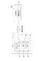
- image display processing may be executed by a computer 314 in an external device 312 communicably connected to the camera 1 via a network 310 such as LAN or WAN.
- computer 314 comprises CPU 316 , storage 318 and memory 320 .
- the storage 318 stores the image display processing program 100 .
- the camera 1 requests execution of image display processing from the external device 312 via the network 310 .
- CPU 316 of external device 312 reads image display processing program 100 from storage 318 and executes image display processing program 100 on memory 320 .
- the CPU 316 performs image display processing according to the image display processing program 100 executed on the memory 320 .
- the CPU 316 provides the camera 1 with the processing result obtained by executing the image display processing via the network 310 .
- the image display processing may be performed by the camera 1 and the external device 312 in a distributed manner, or the image display processing may be performed by the camera 1 and a plurality of devices including the external device 312 in a distributed manner.
- the camera 1 and the external device 312 are examples of the “imaging device” according to the technology of the present disclosure.
- the NVM 62 stores the image display processing program 100 as an example, but the technology of the present disclosure is not limited to this.
- the image display processing program 100 may be stored in the storage medium 330 as shown in FIG.
- Storage medium 330 is a non-temporary storage medium.
- An example of the storage medium 330 includes any portable storage medium such as an SSD or USB memory.
- the image display processing program 100 stored in the storage medium 330 is installed in the computer 60.
- the CPU 61 executes image display processing according to the image display processing program 100 .
- the image display processing program 100 is stored in a storage unit such as another computer or a server device connected to the computer 60 via a communication network (not shown), and the image display processing program is executed in response to a request from the camera 1. 100 may be downloaded and installed on computer 60 .
- FIG. 20 shows an aspect example in which the computer 60 is built in the camera 1, the technology of the present disclosure is not limited to this. may be made available.
- the CPU 61 is a single CPU, but may be a plurality of CPUs. Also, a GPU may be applied instead of the CPU 61 .
- the computer 60 is illustrated in the example shown in FIG. good too. Also, instead of the computer 60, a combination of hardware configuration and software configuration may be used.
- the processor includes, for example, a CPU, which is a general-purpose processor that functions as a hardware resource that executes image display processing by executing software, that is, a program.
- processors include, for example, FPGAs, PLDs, ASICs, and other dedicated electric circuits that are processors having circuit configurations specially designed to execute specific processing.
- a memory is built in or connected to each processor, and each processor executes image display processing by using the memory.
- the hardware resource that executes image display processing may be configured with one of these various processors, or a combination of two or more processors of the same or different type (for example, a combination of multiple FPGAs, or (combination of CPU and FPGA). Also, the hardware resource for executing image display processing may be one processor.
- one processor is configured by combining one or more CPUs and software, and this processor functions as a hardware resource for executing image display processing.
- this processor functions as a hardware resource for executing image display processing.
- SoC SoC
- a and/or B is synonymous with “at least one of A and B.” That is, “A and/or B” means that only A, only B, or a combination of A and B may be used. Also, in this specification, when three or more matters are expressed by connecting with “and/or”, the same idea as “A and/or B" is applied.
- Appendix 1 a processor; a memory connected to or embedded in the processor;
- the processor acquires a first image by causing an image sensor of an imaging device to capture a first light and acquires a second image by causing the image sensor to capture a second light.
- a second mode to the first mode is a mode in which shape information of a subject is represented in the first image in a first gradation;
- the imaging control device wherein the second mode is a mode in which temperature information of the subject is expressed in the second image in a second gradation.
Abstract
Description
プロセッサと、
前記プロセッサに接続又は内蔵されたメモリと、を備え、
前記プロセッサは、撮像装置のイメージセンサに対して第1光を撮像させることにより第1画像を取得する第1モードと、前記イメージセンサに対して第2光を撮像させることにより第2画像を取得する第2モードとを有し、
前記第1モードは、前記第1画像に被写体の形状情報を第1階調で表させるモードであり、
前記第2モードは、前記第2画像に前記被写体の温度情報を第2階調で表させるモードである
撮像制御装置。
Claims (18)
- プロセッサと、
前記プロセッサに接続又は内蔵されたメモリと、を備え、
前記プロセッサは、
撮像装置のイメージセンサに対して第1感度で第1光を撮像させることにより第1画像を取得し、
前記イメージセンサに対して第2感度で第2光を撮像させることにより第2画像を取得し、
前記第1感度は、前記第1画像に被写体の形状情報を第1階調で表させる感度であり、
前記第2感度は、前記第2画像に前記被写体の温度情報を第2階調で表させる感度である
撮像制御装置。 - 前記形状情報は、輪郭情報を含む
請求項1に記載の撮像制御装置。 - 前記プロセッサは、前記第1画像及び前記第2画像に基づいて合成画像を生成する
請求項1又は請求項2に記載の撮像制御装置。 - 前記プロセッサは、前記温度情報に対応する温度分布情報を生成し、
前記合成画像は、前記形状情報及び前記温度分布情報を表す画像である
請求項3に記載の撮像制御装置。 - 前記合成画像は、前記第1画像に前記温度分布情報を重畳した画像である
請求項4に記載の撮像制御装置。 - 前記温度分布情報は、温度分布を視覚的な特徴量で表す情報である
請求項4又は請求項5に記載の撮像制御装置。 - 前記温度分布情報は、半透明画像である
請求項4から請求項6の何れか一項に記載の撮像制御装置。 - 前記プロセッサは、前記合成画像をディスプレイに表示させるための表示データを出力する
請求項3から請求項7の何れか一項に記載の撮像制御装置。 - 前記プロセッサは、前記第1画像を取得する第1頻度を、前記第2画像を取得する第2頻度よりも高く設定する
請求項1から請求項8の何れか一項に記載の撮像制御装置。 - 前記第1感度及び前記第2感度は、前記イメージセンサによって撮像が行われることで得られる撮像信号の信号増幅率に基づいて規定されている
請求項1から請求項9の何れか一項に記載の撮像制御装置。 - 前記第1感度に対応する前記信号増幅率は、対数関数的に規定されており、
前記第2感度に対応する前記信号増幅率は、指数関数的に規定されている
請求項10に記載の撮像制御装置。 - 前記第1感度は、前記第2感度よりも高い
請求項1から請求項11の何れか一項に記載の撮像制御装置。 - 前記プロセッサは、外部からの指示、又は前記被写体から得られる情報に基づいて、前記第1感度及び前記第2感度のうちの少なくとも一方を変更する
請求項1から請求項12の何れか一項に記載の撮像制御装置。 - 前記第1光及び前記第2光は、それぞれ近赤外光である
請求項1から請求項13の何れか一項に記載の撮像制御装置。 - 前記イメージセンサによって受光される光の量を変更する絞り機構をさらに有し、
前記第1感度及び前記第2感度は、前記光の量の変更に基づいて規定されている
請求項1から請求項9の何れか一項に記載の撮像制御装置。 - 請求項1から請求項15の何れか一項に記載の撮像制御装置と、
前記撮像制御装置によって制御される前記イメージセンサと、
を備える撮像装置。 - 撮像装置のイメージセンサに対して第1感度で第1光を撮像させることにより第1画像を取得すること、及び、
前記イメージセンサに対して第2感度で第2光を撮像させることにより第2画像を取得すること、を備え、
前記第1感度は、前記第1画像に被写体の形状情報を第1階調で表させる感度であり、
前記第2感度は、前記第2画像に前記被写体の温度情報を第2階調で表させる感度である
撮像制御方法。 - コンピュータに、処理を実行させるためのプログラムであって、
前記処理は、
撮像装置のイメージセンサに対して第1感度で第1光を撮像させることにより第1画像を取得すること、及び、
前記イメージセンサに対して第2感度で第2光を撮像させることにより第2画像を取得すること、を備え、
前記第1感度は、前記第1画像に被写体の形状情報を第1階調で表させる感度であり、
前記第2感度は、前記第2画像に前記被写体の温度情報を第2階調で表させる感度である
プログラム。
Priority Applications (3)
| Application Number | Priority Date | Filing Date | Title |
|---|---|---|---|
| CN202280022847.2A CN117044219A (zh) | 2021-03-31 | 2022-01-12 | 摄像控制装置、摄像装置、摄像控制方法及程序 |
| JP2023510286A JPWO2022209125A1 (ja) | 2021-03-31 | 2022-01-12 | |
| US18/472,255 US20240015377A1 (en) | 2021-03-31 | 2023-09-22 | Imaging control device, imaging apparatus, imaging control method, and program |
Applications Claiming Priority (2)
| Application Number | Priority Date | Filing Date | Title |
|---|---|---|---|
| JP2021061522 | 2021-03-31 | ||
| JP2021-061522 | 2021-03-31 |
Related Child Applications (1)
| Application Number | Title | Priority Date | Filing Date |
|---|---|---|---|
| US18/472,255 Continuation US20240015377A1 (en) | 2021-03-31 | 2023-09-22 | Imaging control device, imaging apparatus, imaging control method, and program |
Publications (1)
| Publication Number | Publication Date |
|---|---|
| WO2022209125A1 true WO2022209125A1 (ja) | 2022-10-06 |
Family
ID=83456001
Family Applications (1)
| Application Number | Title | Priority Date | Filing Date |
|---|---|---|---|
| PCT/JP2022/000784 WO2022209125A1 (ja) | 2021-03-31 | 2022-01-12 | 撮像制御装置、撮像装置、撮像制御方法、及びプログラム |
Country Status (4)
| Country | Link |
|---|---|
| US (1) | US20240015377A1 (ja) |
| JP (1) | JPWO2022209125A1 (ja) |
| CN (1) | CN117044219A (ja) |
| WO (1) | WO2022209125A1 (ja) |
Citations (4)
| Publication number | Priority date | Publication date | Assignee | Title |
|---|---|---|---|---|
| JP2006185410A (ja) * | 2004-12-02 | 2006-07-13 | Nissan Motor Co Ltd | 夜間移動体報知装置及び夜間移動体報知方法 |
| JP2007208776A (ja) * | 2006-02-03 | 2007-08-16 | Nikon Corp | カメラ |
| WO2019203351A1 (ja) * | 2018-04-20 | 2019-10-24 | パナソニックIpマネジメント株式会社 | 画像表示装置及び画像表示方法 |
| JP2020062198A (ja) * | 2018-10-17 | 2020-04-23 | 鹿島建設株式会社 | 状態判定システム |
-
2022
- 2022-01-12 CN CN202280022847.2A patent/CN117044219A/zh active Pending
- 2022-01-12 WO PCT/JP2022/000784 patent/WO2022209125A1/ja active Application Filing
- 2022-01-12 JP JP2023510286A patent/JPWO2022209125A1/ja active Pending
-
2023
- 2023-09-22 US US18/472,255 patent/US20240015377A1/en active Pending
Patent Citations (4)
| Publication number | Priority date | Publication date | Assignee | Title |
|---|---|---|---|---|
| JP2006185410A (ja) * | 2004-12-02 | 2006-07-13 | Nissan Motor Co Ltd | 夜間移動体報知装置及び夜間移動体報知方法 |
| JP2007208776A (ja) * | 2006-02-03 | 2007-08-16 | Nikon Corp | カメラ |
| WO2019203351A1 (ja) * | 2018-04-20 | 2019-10-24 | パナソニックIpマネジメント株式会社 | 画像表示装置及び画像表示方法 |
| JP2020062198A (ja) * | 2018-10-17 | 2020-04-23 | 鹿島建設株式会社 | 状態判定システム |
Also Published As
| Publication number | Publication date |
|---|---|
| US20240015377A1 (en) | 2024-01-11 |
| JPWO2022209125A1 (ja) | 2022-10-06 |
| CN117044219A (zh) | 2023-11-10 |
Similar Documents
| Publication | Publication Date | Title |
|---|---|---|
| JP3791777B2 (ja) | 電子内視鏡 | |
| JP3958603B2 (ja) | 電子内視鏡システム及び電子内視鏡システム用の信号処理装置 | |
| JP2021192534A (ja) | 撮像装置及び撮像方法 | |
| US20170075050A1 (en) | Imaging device | |
| JP5053468B2 (ja) | 立体画像撮影装置および内視鏡 | |
| JP2013534083A (ja) | 2センサー撮像システム | |
| JP4971532B1 (ja) | 立体画像撮影装置および内視鏡 | |
| KR102036895B1 (ko) | 카메라 어셈블리 및 이를 이용한 영상획득방법 | |
| JP2007214964A (ja) | 映像表示装置 | |
| CN103126654A (zh) | 一种近红外体表血管检测仪的检测系统 | |
| JP2014185917A (ja) | 撮像装置 | |
| JP7442985B2 (ja) | カメラスコープ電子可変プリズム | |
| WO2016052101A1 (ja) | 撮像装置および画像データ生成プログラム | |
| JP2020006177A (ja) | カメラスコープ電子可変プリズム | |
| WO2019187958A1 (ja) | 情報検出装置、映像投影装置、情報検出方法、及び映像投影方法 | |
| JPWO2018163500A1 (ja) | 内視鏡装置 | |
| JP7012549B2 (ja) | 内視鏡装置、内視鏡装置の制御方法、内視鏡装置の制御プログラム、および記録媒体 | |
| JP2007121625A (ja) | 画像表示装置 | |
| WO2019078338A1 (ja) | 電子機器 | |
| US10122990B2 (en) | Imaging system and method of producing context and focus images | |
| WO2022209125A1 (ja) | 撮像制御装置、撮像装置、撮像制御方法、及びプログラム | |
| JP2008123257A (ja) | 遠隔作業支援システム、表示制御方法 | |
| JP2005148265A (ja) | カメラ装置 | |
| JP5948232B2 (ja) | 撮像装置 | |
| JP4358531B2 (ja) | 内視鏡装置 |
Legal Events
| Date | Code | Title | Description |
|---|---|---|---|
| 121 | Ep: the epo has been informed by wipo that ep was designated in this application |
Ref document number: 22779358 Country of ref document: EP Kind code of ref document: A1 |
|
| WWE | Wipo information: entry into national phase |
Ref document number: 2023510286 Country of ref document: JP |
|
| WWE | Wipo information: entry into national phase |
Ref document number: 202280022847.2 Country of ref document: CN |
|
| NENP | Non-entry into the national phase |
Ref country code: DE |
|
| 122 | Ep: pct application non-entry in european phase |
Ref document number: 22779358 Country of ref document: EP Kind code of ref document: A1 |