WO2022202808A1 - 抵抗体、可変抵抗器および抵抗体の製造方法 - Google Patents
抵抗体、可変抵抗器および抵抗体の製造方法 Download PDFInfo
- Publication number
- WO2022202808A1 WO2022202808A1 PCT/JP2022/013135 JP2022013135W WO2022202808A1 WO 2022202808 A1 WO2022202808 A1 WO 2022202808A1 JP 2022013135 W JP2022013135 W JP 2022013135W WO 2022202808 A1 WO2022202808 A1 WO 2022202808A1
- Authority
- WO
- WIPO (PCT)
- Prior art keywords
- resistor
- rich layer
- polishing
- coating
- conductor
- Prior art date
- Legal status (The legal status is an assumption and is not a legal conclusion. Google has not performed a legal analysis and makes no representation as to the accuracy of the status listed.)
- Ceased
Links
Images
Classifications
-
- H—ELECTRICITY
- H01—ELECTRIC ELEMENTS
- H01C—RESISTORS
- H01C7/00—Non-adjustable resistors formed as one or more layers or coatings; Non-adjustable resistors made from powdered conducting material or powdered semi-conducting material with or without insulating material
- H01C7/06—Non-adjustable resistors formed as one or more layers or coatings; Non-adjustable resistors made from powdered conducting material or powdered semi-conducting material with or without insulating material including means to minimise changes in resistance with changes in temperature
-
- H—ELECTRICITY
- H01—ELECTRIC ELEMENTS
- H01C—RESISTORS
- H01C10/00—Adjustable resistors
-
- H—ELECTRICITY
- H01—ELECTRIC ELEMENTS
- H01C—RESISTORS
- H01C17/00—Apparatus or processes specially adapted for manufacturing resistors
- H01C17/06—Apparatus or processes specially adapted for manufacturing resistors adapted for coating resistive material on a base
- H01C17/065—Apparatus or processes specially adapted for manufacturing resistors adapted for coating resistive material on a base by thick film techniques, e.g. serigraphy
-
- H—ELECTRICITY
- H01—ELECTRIC ELEMENTS
- H01C—RESISTORS
- H01C7/00—Non-adjustable resistors formed as one or more layers or coatings; Non-adjustable resistors made from powdered conducting material or powdered semi-conducting material with or without insulating material
- H01C7/006—Thin film resistors
Definitions
- the present invention relates to a resistor, a variable resistor, and a method for manufacturing a resistor.
- Patent Document 1 discloses an insulating layer formed on the surface of a metal plate, a resistor formed as a coating on the insulating layer, and a metal brush that can be moved to any position on the resistor.
- a variable resistor with contacts (sliders) is disclosed.
- An object of the present invention is to provide a resistor, a variable resistor, and a method of manufacturing a resistor capable of realizing lead-free use and preventing deterioration of sliding characteristics.
- the resistor in the present invention is A resistor disposed on the insulating layer,
- the resistor has a conductive material-rich layer containing more conductive material than an insulating material, and an insulating material-rich layer that does not contain lead and contains more of the insulating material than the conductive material,
- the conductor-rich layer has a polished surface.
- variable resistor in the present invention is Equipped with the above resistor.
- the method for manufacturing a resistor in the present invention includes: Forming a film on the insulating layer with a lead-free resistor ink, The film surface of the coating is polished so that the polishing amount of the coating is in the range of 0.1% to 10% with respect to the coating amount of the coating.
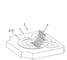
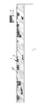
- FIG. 1 is a perspective view showing an example of a variable resistor according to an embodiment of the invention.
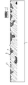
- FIG. 2A is a cross-sectional view of the low resistance region before polishing.
- FIG. 2B is a cross-sectional view of the low resistance region after polishing.
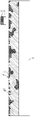
- FIG. 3A is a cross-sectional view of the high resistance region before polishing.
- FIG. 3B is a cross-sectional view of the high resistance region after polishing.
- FIG. 1 is a perspective view showing an example of a variable resistor 1 according to an embodiment of the invention.
- a variable resistor 1 comprises a ceramic substrate 2 which is an insulating layer, a resistor 3 formed as a film on the ceramic substrate 2, and contacts movable to arbitrary positions on the resistor. 4 (slider).
- the resistor 3 is formed on the ceramic substrate 2 with resistor ink.
- the resistor 3 has a conductor-rich layer 5 containing more conductors than insulators and an insulator-rich layers 6 containing more insulators than conductors (see FIGS. 2A and 2B).
- the conductor-rich layer 5 and the insulator-rich layer 6 are collectively referred to as "coatings".
- a method for manufacturing the resistor 3 will be described.
- a lead-free resistor ink is applied onto the ceramic substrate 2, and then baked to form the conductor-rich layer 5 and the insulator-rich layer 6.
- the resistor ink for example, a conductive material made of paste of silver, copper, or a hybrid of silver and copper and an insulating material made of lead-free glass paste are blended.
- the resistor coating after printing the resistor ink has a predetermined roughness with peaks and valleys.
- the surface of the resistor 3 is composed of the film surface (mountain) of the conductor-rich layer 5 and the insulator-rich layer 6 .
- the surface of the resistor 3 is simply referred to as "film surface of the coating”.
- the film surface of the film is polished.
- the surface of the resistor 3 is polished.
- known means such as buffing, barrel polishing, and lapping are used. Polishing of the film surface is performed while measuring the resistance value of the film.
- the amount of polishing is 0.1% to 10% of the amount of coating before polishing (the amount of coating of the conductive material-rich layer 5 and the coating amount of the insulating material-rich layer 6).
- the polishing amount is preferably 0.1% to 3%.
- the amount of polishing is the amount of increase in the resistance value of the film after polishing relative to the resistance value of the film in the low resistance region 7 (the film of the conductive material-rich layer 5 and the insulating material-rich layer 6) before polishing (0 .1% to 10%).
- the resistor 3 has a low resistance region 7 having a resistance value (eg, 10 ⁇ to 10 k ⁇ ) and a high resistance region 8 having a resistance value (eg, 1 k ⁇ to 5 M ⁇ ).
- the manufacturing method is basically the same, but the thickness of each of the conductor-rich layer 5 and the insulator-rich layer 6 and the polishing of the film surface is different.
- FIG. 2A is a cross-sectional view of the low resistance region 7 before polishing.
- FIG. 2B is a cross-sectional view of the low resistance region 7 after polishing.
- FIG. 3A is a cross-sectional view of high resistance region 8 before polishing.
- FIG. 3B is a cross-sectional view of the high resistance region 8 after polishing.
- the insulator-rich layer 6 in the low resistance region 7 is thinner than the insulator-rich layer 6 in the high resistance region 8 .
- the ratio of the film surface area of the conductor-rich layer 5 to the surface area of the resistor 3 before polishing is larger in the low resistance region 7 than in the high resistance region 8 . This is because the ink for low resistance contains more conductive materials and less insulating material, while the ink for higher resistance contains less conductive material and requires more insulation.
- the top of the conductor-rich layer 5 is polished in the film surface polishing of the low resistance region 7.
- the cross-sectional area of the conductor-rich layer 5 is reduced, and the total resistance value is increased.
- wear of the contact 4 is reduced.
- the total resistance value of the resistor 3 is set to be low in advance so that it becomes an appropriate value after polishing.
- the top of the conductor-rich layer 5 is polished in the film surface polishing of the high resistance region 8.
- the cross section of the conductor-rich layer 5 is reduced, and the total resistance value is increased.
- wear of the contact 4 see FIG. 1 is reduced.
- the film surface of the insulator-rich layer 6 is polished, the roughness of the film surface is reduced by removing the vitreous substance in contact with the contact 4, so that the abrasion of the contact 4 can be reduced. Dynamic characteristics can be improved.
- the total resistance value of the resistor 3 is set to be low in advance so that it becomes an appropriate value after polishing.
- the resistor 3 is a resistor formed on the ceramic substrate 2 as a film (a conductor-rich layer 5 and an insulator-rich layer 6 that does not contain lead). It has a polished film surface, and the polishing amount of the coating is in the range of 0.1% to 10% with respect to the coating amount before polishing.
- the resistor is formed as the conductive substance-rich layer 5 and the insulator-rich layer 6 that does not contain lead, so it is possible to realize lead-free. Further, by polishing the film surface of the film, the roughness of the film surface is reduced, so that the wear of the contact 4 can be reduced and deterioration of the sliding characteristics can be prevented.
- the polishing amount of the film is determined based on the amount of increase in the resistance value of the film after polishing with respect to the resistance value of the film before polishing. This makes it possible to polish a predetermined amount by polishing the film surface while referring to the amount of increase in the resistance value.
- the film includes the conductor-rich layer 5 formed of a conductive substance, and the insulator-rich layer 5 formed of an insulating substance on the conductor-rich layer 5. and a containing layer 6 . Since the roughness of the film surface of the conductor-rich layer 5 is larger than that of the insulator-rich layer 6, depending on the film thickness of the conductor-rich layer 5, the peak of the film surface of the conductor-rich layer 5 is exposed without being covered with the insulator-rich layer 6 . This makes it possible to adjust the resistance value of the film according to the amount of polishing of the film surface of the conductor-rich layer 5 .
- the conductor-rich layer 5 has a polished film surface. By polishing the top of the film surface of the conductor-rich layer 5, the resistance value of the coating can be adjusted. In this case, the film surface of the insulator-rich layer 6 may or may not be polished.
- the resistance value of the film is adjusted by polishing only the film surface (mountain) of the conductor-rich layer 5, but the conductor-rich layer 5 and the insulator
- Each film surface of the multi-containing layer 6 may be polished.
- polishing the insulating material-rich layer 6, for example vitreous material is removed from the film surface, so that the roughness of the film surface is reduced, the wear of the contacts 4 is reduced, and the sliding characteristics can be further improved. It becomes possible.
- the present invention is suitable for variable resistors equipped with resistors that are required to be lead-free and prevent deterioration of sliding characteristics.
Landscapes
- Engineering & Computer Science (AREA)
- Microelectronics & Electronic Packaging (AREA)
- Manufacturing & Machinery (AREA)
- Physics & Mathematics (AREA)
- Electromagnetism (AREA)
- Adjustable Resistors (AREA)
- Apparatuses And Processes For Manufacturing Resistors (AREA)
- Non-Adjustable Resistors (AREA)
- Thermistors And Varistors (AREA)
- Electronic Switches (AREA)
Abstract
Description
絶縁性層の上に配置された抵抗体であって、
前記抵抗体は、絶縁物よりも導電物を多く含む導電物多含有層と、鉛を含まず、前記導電物よりも前記絶縁物を多く含む絶縁物多含有層とを有し、
前記導電物多含有層は、研磨された面を有する。
上記の抵抗体を備える。
絶縁性層の上に鉛を含まない抵抗体インクにより被膜を形成し、
前記被膜の研磨量が前記被膜の被膜量に対して0.1%から10%の範囲となるように前記被膜の膜面を研磨する。
図1は、本発明の実施の形態に係る可変抵抗器1の一例を示す斜視図である。
先ず、セラミック基板2の上に鉛を含まない抵抗体インクを塗布し、塗布後に焼き付けることにより導電物多含有層5および絶縁物多含有層6を形成する。抵抗体インクとしては、例えば、銀や、銅や、銀と銅のハイブリットのペーストによる導電性物質と、鉛を含まないガラスペーストによる絶縁物質が配合される。
図2Aおよび図3Aに示すように、研磨前においては、低抵抗域7の絶縁物多含有層6の膜厚は、高抵抗域8の絶縁物多含有層6の膜厚よりも薄い。これにより、研磨前の抵抗体3の表面面積に対する導電物多含有層5の膜面面積の割合は、低抵抗域7の方が高抵抗域8よりも大きい。これは、低抵抗向けのインクは導電性材料が多く、絶縁材料が少ない、一方、高抵抗向けは、導電性材料が少なく、絶縁税量が多い、材料比率の違いによるものである。
2 セラミック基板
3 抵抗体
4 接点(摺動子)
5 導電物多含有層
6 絶縁物多含有層
7 低抵抗域
8 高抵抗域
Claims (5)
- 絶縁性層の上に配置された抵抗体であって、
前記抵抗体は、絶縁物よりも導電物を多く含む導電物多含有層と、鉛を含まず、前記導電物よりも前記絶縁物を多く含む絶縁物多含有層とを有し、
前記導電物多含有層は、研磨された面を有する、
抵抗体。 - 抵抗値が所定値以下である低抵抗域の前記導電物多含有層の膜厚は、抵抗値が所定値よりも高い高抵抗域の前記絶縁物多含有層の膜厚よりも厚い、
請求項1に記載の抵抗体。 - 請求項1に記載の抵抗体を備える、可変抵抗器。
- 絶縁性層の上に鉛を含まない抵抗体インクにより被膜を形成し、
前記被膜の研磨量が前記被膜の被膜量に対して0.1%から10%の範囲となるように前記被膜の膜面を研磨する、
抵抗体の製造方法。 - 前記研磨量は、研磨前の前記被膜の抵抗値に対する研磨後の前記被膜の抵抗値の増加量に基づいて定められる、
請求項4に記載の抵抗体の製造方法。
Priority Applications (3)
| Application Number | Priority Date | Filing Date | Title |
|---|---|---|---|
| US18/283,013 US20240153679A1 (en) | 2021-03-25 | 2022-03-22 | Resistor, variable resistor, and method for manufacturing resistor |
| CN202280022126.1A CN117121132A (zh) | 2021-03-25 | 2022-03-22 | 电阻体、可变电阻器、以及电阻体的制造方法 |
| JP2023509194A JPWO2022202808A1 (ja) | 2021-03-25 | 2022-03-22 |
Applications Claiming Priority (2)
| Application Number | Priority Date | Filing Date | Title |
|---|---|---|---|
| JP2021051256 | 2021-03-25 | ||
| JP2021-051256 | 2021-03-25 |
Publications (1)
| Publication Number | Publication Date |
|---|---|
| WO2022202808A1 true WO2022202808A1 (ja) | 2022-09-29 |
Family
ID=83395615
Family Applications (1)
| Application Number | Title | Priority Date | Filing Date |
|---|---|---|---|
| PCT/JP2022/013135 Ceased WO2022202808A1 (ja) | 2021-03-25 | 2022-03-22 | 抵抗体、可変抵抗器および抵抗体の製造方法 |
Country Status (5)
| Country | Link |
|---|---|
| US (1) | US20240153679A1 (ja) |
| JP (1) | JPWO2022202808A1 (ja) |
| CN (1) | CN117121132A (ja) |
| TW (1) | TW202238631A (ja) |
| WO (1) | WO2022202808A1 (ja) |
Citations (8)
| Publication number | Priority date | Publication date | Assignee | Title |
|---|---|---|---|---|
| JPS51147255U (ja) * | 1975-05-20 | 1976-11-26 | ||
| JPS53145142U (ja) * | 1977-04-21 | 1978-11-15 | ||
| JPS63260101A (ja) * | 1987-02-05 | 1988-10-27 | レダ ロガリスミック エレクトリカル ディバイスィズ フォー オートメイション ソチエタ レスポンサビリタ リミテ | 電気抵抗体の製造方法 |
| JPH03165002A (ja) * | 1989-11-24 | 1991-07-17 | Matsushita Electric Ind Co Ltd | 高電力用抵抗体および可変抵抗器 |
| JPH06350218A (ja) * | 1993-06-08 | 1994-12-22 | Tdk Corp | 配線基板およびその製造方法 |
| JP2015002212A (ja) * | 2013-06-13 | 2015-01-05 | ローム株式会社 | チップ抵抗器、チップ抵抗器の実装構造 |
| JP2018098412A (ja) * | 2016-12-15 | 2018-06-21 | 住友金属鉱山株式会社 | 厚膜抵抗体用組成物、厚膜抵抗体用ペースト、厚膜抵抗体およびこれらの製造方法 |
| JP2020170817A (ja) * | 2019-04-05 | 2020-10-15 | Koa株式会社 | 抵抗材料、抵抗器及び抵抗材料の製造方法 |
-
2022
- 2022-03-22 WO PCT/JP2022/013135 patent/WO2022202808A1/ja not_active Ceased
- 2022-03-22 JP JP2023509194A patent/JPWO2022202808A1/ja active Pending
- 2022-03-22 CN CN202280022126.1A patent/CN117121132A/zh active Pending
- 2022-03-22 US US18/283,013 patent/US20240153679A1/en active Pending
- 2022-03-24 TW TW111111020A patent/TW202238631A/zh unknown
Patent Citations (8)
| Publication number | Priority date | Publication date | Assignee | Title |
|---|---|---|---|---|
| JPS51147255U (ja) * | 1975-05-20 | 1976-11-26 | ||
| JPS53145142U (ja) * | 1977-04-21 | 1978-11-15 | ||
| JPS63260101A (ja) * | 1987-02-05 | 1988-10-27 | レダ ロガリスミック エレクトリカル ディバイスィズ フォー オートメイション ソチエタ レスポンサビリタ リミテ | 電気抵抗体の製造方法 |
| JPH03165002A (ja) * | 1989-11-24 | 1991-07-17 | Matsushita Electric Ind Co Ltd | 高電力用抵抗体および可変抵抗器 |
| JPH06350218A (ja) * | 1993-06-08 | 1994-12-22 | Tdk Corp | 配線基板およびその製造方法 |
| JP2015002212A (ja) * | 2013-06-13 | 2015-01-05 | ローム株式会社 | チップ抵抗器、チップ抵抗器の実装構造 |
| JP2018098412A (ja) * | 2016-12-15 | 2018-06-21 | 住友金属鉱山株式会社 | 厚膜抵抗体用組成物、厚膜抵抗体用ペースト、厚膜抵抗体およびこれらの製造方法 |
| JP2020170817A (ja) * | 2019-04-05 | 2020-10-15 | Koa株式会社 | 抵抗材料、抵抗器及び抵抗材料の製造方法 |
Also Published As
| Publication number | Publication date |
|---|---|
| CN117121132A (zh) | 2023-11-24 |
| US20240153679A1 (en) | 2024-05-09 |
| JPWO2022202808A1 (ja) | 2022-09-29 |
| TW202238631A (zh) | 2022-10-01 |
Similar Documents
| Publication | Publication Date | Title |
|---|---|---|
| US2134870A (en) | Resistance element | |
| JP3426227B2 (ja) | 混合セラミックス層を有する帯電ローラの製造方法 | |
| US20070217117A1 (en) | Electrostatic chuck and producing method thereof | |
| JPH04118901A (ja) | 正特性サーミスタおよびその製造方法 | |
| WO2022202808A1 (ja) | 抵抗体、可変抵抗器および抵抗体の製造方法 | |
| US3200010A (en) | Electrical resistance element | |
| US20250285808A1 (en) | Multilayer ceramic capacitor | |
| CN117015835A (zh) | 复合热敏电阻元件 | |
| HK40099256A (zh) | 电阻体、可变电阻器、以及电阻体的制造方法 | |
| US2211583A (en) | Method of making electric condensers and condensers made thereby | |
| JP2023035178A (ja) | バリスタ及びその製造方法 | |
| JPH03211802A (ja) | スイッチ付可変抵抗器 | |
| JP4117146B2 (ja) | 摺動部を有する入力装置 | |
| TWI904915B (zh) | 積層陶瓷電子零件 | |
| CN116631715A (zh) | 电阻器组件及用于制造电阻器组件的方法 | |
| CN101084559A (zh) | 变阻器的制造方法 | |
| TWM618287U (zh) | 多層式壓敏電阻 | |
| US4948529A (en) | Stable high resistance transparent coating | |
| JPH05242958A (ja) | 定着ヒーターおよびその製造方法 | |
| US20230274863A1 (en) | Multilayer varistor | |
| US2984589A (en) | Electrical resistors | |
| JP2523665B2 (ja) | 電圧非直線抵抗器の製造方法 | |
| WO2025089298A1 (ja) | 電子部品、保護膜の成膜方法、及び電子部品の製造方法 | |
| JP2001242001A (ja) | 印刷抵抗基板およびこの印刷抵抗基板を用いた検出器 | |
| JPS60165010A (ja) | 摺動接点用回路板 |
Legal Events
| Date | Code | Title | Description |
|---|---|---|---|
| 121 | Ep: the epo has been informed by wipo that ep was designated in this application |
Ref document number: 22775591 Country of ref document: EP Kind code of ref document: A1 |
|
| WWE | Wipo information: entry into national phase |
Ref document number: 2023509194 Country of ref document: JP |
|
| WWE | Wipo information: entry into national phase |
Ref document number: 18283013 Country of ref document: US |
|
| NENP | Non-entry into the national phase |
Ref country code: DE |
|
| 122 | Ep: pct application non-entry in european phase |
Ref document number: 22775591 Country of ref document: EP Kind code of ref document: A1 |