WO2022202659A1 - ワークの処理方法 - Google Patents
ワークの処理方法 Download PDFInfo
- Publication number
- WO2022202659A1 WO2022202659A1 PCT/JP2022/012587 JP2022012587W WO2022202659A1 WO 2022202659 A1 WO2022202659 A1 WO 2022202659A1 JP 2022012587 W JP2022012587 W JP 2022012587W WO 2022202659 A1 WO2022202659 A1 WO 2022202659A1
- Authority
- WO
- WIPO (PCT)
- Prior art keywords
- temporary fixing
- work
- fixing material
- support
- workpiece
- Prior art date
- Legal status (The legal status is an assumption and is not a legal conclusion. Google has not performed a legal analysis and makes no representation as to the accuracy of the status listed.)
- Ceased
Links
Images


Classifications
-
- B—PERFORMING OPERATIONS; TRANSPORTING
- B32—LAYERED PRODUCTS
- B32B—LAYERED PRODUCTS, i.e. PRODUCTS BUILT-UP OF STRATA OF FLAT OR NON-FLAT, e.g. CELLULAR OR HONEYCOMB, FORM
- B32B27/00—Layered products comprising a layer of synthetic resin
-
- B—PERFORMING OPERATIONS; TRANSPORTING
- B32—LAYERED PRODUCTS
- B32B—LAYERED PRODUCTS, i.e. PRODUCTS BUILT-UP OF STRATA OF FLAT OR NON-FLAT, e.g. CELLULAR OR HONEYCOMB, FORM
- B32B7/00—Layered products characterised by the relation between layers; Layered products characterised by the relative orientation of features between layers, or by the relative values of a measurable parameter between layers, i.e. products comprising layers having different physical, chemical or physicochemical properties; Layered products characterised by the interconnection of layers
- B32B7/04—Interconnection of layers
- B32B7/06—Interconnection of layers permitting easy separation
-
- C—CHEMISTRY; METALLURGY
- C09—DYES; PAINTS; POLISHES; NATURAL RESINS; ADHESIVES; COMPOSITIONS NOT OTHERWISE PROVIDED FOR; APPLICATIONS OF MATERIALS NOT OTHERWISE PROVIDED FOR
- C09J—ADHESIVES; NON-MECHANICAL ASPECTS OF ADHESIVE PROCESSES IN GENERAL; ADHESIVE PROCESSES NOT PROVIDED FOR ELSEWHERE; USE OF MATERIALS AS ADHESIVES
- C09J201/00—Adhesives based on unspecified macromolecular compounds
-
- C—CHEMISTRY; METALLURGY
- C09—DYES; PAINTS; POLISHES; NATURAL RESINS; ADHESIVES; COMPOSITIONS NOT OTHERWISE PROVIDED FOR; APPLICATIONS OF MATERIALS NOT OTHERWISE PROVIDED FOR
- C09J—ADHESIVES; NON-MECHANICAL ASPECTS OF ADHESIVE PROCESSES IN GENERAL; ADHESIVE PROCESSES NOT PROVIDED FOR ELSEWHERE; USE OF MATERIALS AS ADHESIVES
- C09J5/00—Adhesive processes in general; Adhesive processes not provided for elsewhere, e.g. relating to primers
-
- C—CHEMISTRY; METALLURGY
- C09—DYES; PAINTS; POLISHES; NATURAL RESINS; ADHESIVES; COMPOSITIONS NOT OTHERWISE PROVIDED FOR; APPLICATIONS OF MATERIALS NOT OTHERWISE PROVIDED FOR
- C09J—ADHESIVES; NON-MECHANICAL ASPECTS OF ADHESIVE PROCESSES IN GENERAL; ADHESIVE PROCESSES NOT PROVIDED FOR ELSEWHERE; USE OF MATERIALS AS ADHESIVES
- C09J7/00—Adhesives in the form of films or foils
- C09J7/30—Adhesives in the form of films or foils characterised by the adhesive composition
- C09J7/38—Pressure-sensitive adhesives [PSA]
-
- H—ELECTRICITY
- H10—SEMICONDUCTOR DEVICES; ELECTRIC SOLID-STATE DEVICES NOT OTHERWISE PROVIDED FOR
- H10P—GENERIC PROCESSES OR APPARATUS FOR THE MANUFACTURE OR TREATMENT OF DEVICES COVERED BY CLASS H10
- H10P95/00—Generic processes or apparatus for manufacture or treatments not covered by the other groups of this subclass
Definitions
- the present invention relates to a work processing method for processing a work such as a wafer while the work is fixed to a support via a temporary fixing material. More specifically, the introduction of the support improves the handling of the work.
- the present invention relates to a processing method capable of stably separating workpieces by a relatively simple process such as mechanical separation while being improved and usable in a wide variety of processing processes.
- a peeling method of turning off, a method of peeling by lifting the carrier from one end (mechanical peeling), and the like have been proposed.
- the mechanical peeling method is a method with excellent cost advantage because the apparatus is relatively simple.
- a peeling force is applied at least to the work/temporary bonding material interface and the temporary bonding material/support interface, and it is not always easy to stably peel at the desired interface. . If peeling occurs at an unintended interface (for example, work/temporary bonding material interface), problems such as damage to the support and electronic parts may occur when the support is peeled off.
- an object of the present invention is to provide a workpiece processing method in which workpieces such as wafers are fixed to a support via a temporary fixing material and processed in a state of a laminated body, which is relatively easy to remove such as mechanical peeling.
- a processing method capable of stably separating a work such as a wafer from a laminate by a simple process.
- the present inventors found that in a work processing method in which a workpiece such as a wafer is fixed to a support via a temporary fixing material and processed in the state of a laminate, the support measured under specific conditions /
- the peel strength between the temporary fixing materials and the peel strength between the temporary fixing materials and the work satisfy specific conditions, the work such as a wafer can be stably separated from the laminate by a relatively simple process such as mechanical peeling.
- the inventors have found that it is possible to do so, and have completed the present invention.
- [2] to [13] below are all preferable aspects or embodiments of the present invention.
- [2] The work processing method according to [1], wherein the peel strength P1 is 10 N/25 mm or less.
- [3] The work according to [1] or [2], wherein the temporary fixing material (B) has a different composition between the adhesive layer in contact with the support (A) and the adhesive layer in contact with the work (C). Processing method.
- [4] By separating the work (C) from the laminate (D), the support (A) is separated from the temporary fixing material (B), and then the temporary fixing material (B) remaining on the work (C) is removed.
- the workpiece processing method according to any one of [1] to [3] is achieved.
- [9] The method for treating a workpiece according to any one of [1] to [8], wherein the thickness of the workpiece (C) after treatment in step (2) is 1 ⁇ m or more and 200 ⁇ m or less.
- [12] The method for manufacturing an electronic device according to [11], wherein the electronic device has a structure in which semiconductor chips are stacked.
- the 10° peel strength P 1 between the support (A) / temporary fixing material (B) and the temporary fixing material (B) / work (C ) to the 10 ° peel strength P2, P2 / P1, is 1.1 or more .
- the handling of thin or fragile works such as wafers is improved, and the work such as wafers can be stably processed in a wide variety of processing processes. Peeling or the like can be effectively suppressed, and workpieces such as wafers after processing can be stably separated and taken out by a relatively simple and low-cost process such as mechanical peeling. It is possible to perform a large number and/or a wide variety of processes on workpieces such as wafers with high productivity and yield without damaging electronic components such as functional layers, and production of electronic components such as electronic devices. contribute greatly to the improvement of sexuality.
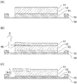
- FIG. 1 is a schematic diagram illustrating separation of a support (A) from a laminate (D) in one embodiment of the present invention, (a) is a preferred separation form, and (b) to (c) are unfavorable separation forms. show.
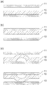
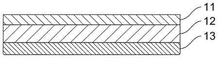
- FIG. 4 is a schematic diagram showing a method for evaluating removability of a temporary fixing material (B) from a work (C) in one example of the present invention. It is a mimetic diagram showing a layered product (D) in one embodiment of the present invention. FIG. 4 is a schematic diagram showing a laminate (D) in another embodiment of the present invention;
- the present invention Step (1) of laminating a support (A), a temporary fixing material (B), and a workpiece (C) located on the opposite side of the temporary fixing material (B) from the support (A) side; From the step (2) of subjecting the work (C) to at least one treatment selected from heat treatment, machining treatment, wet treatment, and laser processing, and the laminate (D) having the work (C) after the treatment , the step (3) of separating the workpiece (C), A method of processing a workpiece having The 10° peel strength P 1 between the support (A) / temporary fixing material (B) and the temporary fixing material (B) / work (C ), the ratio of P 2 /P 1 to the 10 ° peel strength P 2 between is. That is, in the processing method of the present invention, the support (A) and the temporary fixing material (B) as the temporary fixing material are used in processing the workpiece (C).
- Support (A) As the support (A), those having sufficient strength and rigidity and excellent heat resistance and chemical resistance are preferred. By using such a support (A), it is possible to stably handle the work (C) even when the work (C) is thinly ground, and the work (C) can be stably handled without bending or the like. (C) can be subjected to multiple and/or diverse processes. For example, the workpiece (C) having an electronic circuit formed thereon can be subjected to various processes required for manufacturing an electronic device having a structure in which semiconductor chips are stacked, such as TSV connection. Materials preferably used for the support (A) include silicon, sapphire, crystal, metals (eg, aluminum, copper, steel), and various glasses and ceramics.
- the support (A) may consist of a single material, but it may also consist of a plurality of materials and may contain other materials deposited on the substrate. For example, it may have a deposited layer of silicon nitride or the like on a silicon wafer.
- surface treatment such as providing a silicone layer may be performed.
- the support (A) may be made of plastic.
- a sheet made of plastic such as polyimide, acrylic, polyolefin, polycarbonate, vinyl chloride, ABS, polyethylene terephthalate (PET), nylon, or urethane can be preferably used as the support (A). It is particularly preferable to use polyimide because it has a certain degree of heat resistance.
- the thickness of the support (A) is uniform in order to obtain a uniform thickness after grinding the workpiece (C).
- the thickness variation of the support (A) should be suppressed to ⁇ 2 ⁇ m or less.
- the thickness of the support (A) is not particularly limited, it is preferably 300 ⁇ m or more, particularly preferably 500 ⁇ m or more, from the viewpoint of effectively preventing bending of the work (C). From the viewpoint of suppressing the total weight during handling or reducing the stress required for mechanical peeling, the thickness is preferably 1500 ⁇ m or less, particularly preferably 1000 ⁇ m or less.
- Temporary fixing material (B) The temporary fixing material (B) is used for fixing the work (C) to the support (A). It is preferable that the temporary fixing material (B) can be easily peeled off from the support (A) and the workpiece (C). Therefore, the temporary fixing material (B) has sufficient adhesive strength to fix the work (C) to the support (A), but has sufficiently low adhesive strength to be peeled off. preferable.
- an adhesive material for the temporary fixing material (B) includes, for example, rubber, acrylic, epoxy, urethane, allyl, and silicone. , fluorine-based, polyimide-based adhesives, and the like. Among them, acrylic or silicone pressure-sensitive adhesives are preferable because they have heat resistance and can be easily adjusted in adhesive strength and adhesive strength.
- the adhesive material may be a curable adhesive material or a non-curable adhesive material, but by curing before heat treatment, voids are less likely to occur during heat treatment during the manufacturing process. It is preferable to use a curable tacky-adhesive material because it can suppress adhesion enhancement due to high temperature during heat treatment and can be easily peeled off without adhesive residue.
- the curable adhesive material examples include a photocurable adhesive material that is crosslinked and cured by light irradiation and a thermosetting adhesive material that is crosslinked and cured by heating.
- the photocurable adhesive and thermosetting adhesive include monomers, oligomers, and polymers such as acrylic, epoxy, urethane acrylate, epoxy acrylate, silicone acrylate, or polyester acrylate as curing components, Examples include photocurable adhesives and thermosetting adhesives containing photopolymerization initiators and thermal polymerization initiators.
- a (meth)acrylic polymer having a functional group in the molecule (hereinafter referred to as a (meth)acrylic polymer containing a functional group) is synthesized in advance, can be obtained by reacting a compound having a functional group that reacts with the above functional group and a radically polymerizable unsaturated bond (hereinafter referred to as a functional group-containing unsaturated compound).
- the above-mentioned functional group-containing (meth)acrylic polymer is composed mainly of acrylic acid alkyl ester and/or methacrylic acid alkyl ester in which the number of carbon atoms in the alkyl group is usually in the range of 2 to 18, which is combined with a functional group-containing monomer, Furthermore, if necessary, these can be obtained by copolymerizing other copolymerizable monomers for modification by conventional methods.
- the weight average molecular weight of the functional group-containing (meth)acrylic polymer is usually about 200,000 to 2,000,000.
- Examples of the functional group-containing monomer include carboxyl group-containing monomers such as acrylic acid and methacrylic acid, hydroxyl group-containing monomers such as hydroxyethyl acrylate and hydroxyethyl methacrylate, and epoxy compounds such as glycidyl acrylate and glycidyl methacrylate.
- Examples include group-containing monomers, isocyanate group-containing monomers such as isocyanate ethyl acrylate and isocyanate ethyl methacrylate, and amino group-containing monomers such as aminoethyl acrylate and aminoethyl methacrylate.
- Examples of other copolymerizable modifying monomers include various monomers used in general (meth)acrylic polymers such as vinyl acetate, acrylonitrile, and styrene.
- the same functional group-containing monomer as described above is used according to the functional group of the functional group-containing (meth)acrylic polymer.
- the functional group of the functional group-containing (meth)acrylic polymer is a carboxyl group
- an epoxy group-containing monomer or an isocyanate group-containing monomer is used.
- the functional group is a hydroxyl group
- an isocyanate group-containing monomer is used.
- the functional group is an epoxy group
- a carboxyl group-containing monomer or an amide group-containing monomer such as acrylamide is used.
- an epoxy group-containing monomer is used.
- Examples of the photopolymerization initiator include those that are activated by irradiation with light having a wavelength of 250 to 800 nm.
- Examples of such photopolymerization initiators include acetophenone derivative compounds such as methoxyacetophenone, benzoin ether compounds such as benzoin propyl ether and benzoin isobutyl ether, ketal derivative compounds such as benzyl dimethyl ketal and acetophenone diethyl ketal, Phosphine oxide derivative compounds, bis( ⁇ 5-cyclopentadienyl) titanocene derivative compounds, benzophenone, Michler's ketone, chlorothioxanthone, todecylthioxanthone, dimethylthioxanthone, diethylthioxanthone, ⁇ -hydroxycyclohexylphenyl ketone, 2-hydroxymethylphenylpropane and other photoradical polymerization initiators. These photopolymerization initiators may
- thermal polymerization initiator examples include those that are thermally decomposed to generate active radicals that initiate polymerization and curing.
- thermal polymerization initiator examples include those that are thermally decomposed to generate active radicals that initiate polymerization and curing.
- t-butylperoxy-2-ethyl hexanoate bis(4-methylbenzoyl) peroxide, benzoyl peroxide, 1,1-bis(t-hexylperoxy)cyclohexane, 1,1 -bis(t-butylperoxy)cyclohexane, 2,2-bis(4,4-bis-(t-butylperoxy)cyclohexyl)propane, t-hexylperoxyisopropyl monocarboxylate, t-butylperoxyacetate, 2 , 2-bis-(t-butylperoxy)butane, n-butyl 4,4-bis-(t-butylperoxy)pentanoate, bis
- thermal polymerization initiators commercially available ones are not particularly limited. V, Perhexyl D, Permyl D, Perhexa 25B, Perbutyl P, Perbutyl C, Perhexyne 25B, Permyl P (all of these are manufactured by NOF Corp.), Perkadox 12XL25 (manufactured by Kayaku Nourion Co., Ltd.) and the like are suitable. These thermal polymerization initiators may be used alone or in combination of two or more.
- the oligomer or monomer as the curing component generally has a molecular weight of 10,000 or less and 1 to 40 radically polymerizable unsaturated bonds in the molecule.
- the number of radically polymerizable unsaturated bonds is preferably two or more from the viewpoint of three-dimensional networking.
- the oligomer or monomer as the curing component is, for example, trimethylolpropane triacrylate, tetramethylolmethane tetraacrylate, pentaerythritol triacrylate, pentaerythritol tetraacrylate, dipentaerythritol monohydroxypentaacrylate, dipentaerythritol hexaacrylate, or the same as above. and methacrylates of.
- Other examples include 1,4-butylene glycol diacrylate, 1,6-hexanediol diacrylate, polyethylene glycol diacrylate, commercially available oligoester acrylates, urethane acrylates, and methacrylates similar to those described above. These polyfunctional oligomers or monomers may be used alone or in combination of two or more.
- the temporary fixing material (B) may optionally be an acrylic polymer having no unsaturated double bond, various thermal cross-linking agents such as isocyanate compounds, melamine compounds, and epoxy compounds, release agents, plasticizers, resins, and surfactants. , waxes, particulate fillers, and other known additives.
- a release agent from the viewpoint of adjusting the peel strength with (A) the support and/or (C) the work.
- the release agent is not particularly limited as long as it generally exhibits a release effect. Examples thereof include hydrocarbon-based compounds, silicone-based compounds, fluorine-based compounds, and polyethylene-based wax, carnauba wax, montanic acid, and stearic acid, which are known as release agents for plastic materials. Among these, silicone-based and fluorine-based compounds are preferable, and silicone-based and fluorine-based compounds having a functional group capable of cross-linking with the curable adhesive are more preferable.
- silicone compounds are excellent in heat resistance, so they prevent sticking of the adhesive material even after treatment involving heating at 200 ° C. or higher, and bleed out to the adherend interface during peeling, facilitating peeling. do. Since the silicone compound has a functional group that can be crosslinked with the curable adhesive, it chemically reacts with the curable adhesive by light irradiation or heating and is incorporated into the curable adhesive. Silicone compounds do not adhere to the body and contaminate it. In addition, the addition of a silicone compound also exhibits the effect of preventing adhesive residue on the semiconductor chip. Moreover, a plasticizer etc. are mentioned as another release agent. The plasticizer is not particularly limited as long as it generally reduces the adhesive force of the adhesive material to the adherend. Examples thereof include plasticizers such as trimellitic acid esters, pyromellitic acid esters, phthalic acid esters and adipic acid esters.
- the amount of the release agent to be added is not particularly limited, but the amount to be added is appropriately determined so that the release effect can be obtained.
- the addition amount is controlled so as not to excessively impair the adhesive function of the temporary fixing material (B).
- the amount added is usually 0.1 to 5 parts by mass, preferably 0.1 to 3 parts by mass, and more preferably about 0.1 to 1 part by mass. It is desirable to adjust according to the peeling force using as a guide.
- a plasticizer is added, it is usually added in an amount of 5 to 50 parts by mass, preferably 10 to 50 parts by mass, more preferably 20 to 40 parts by mass. It is desirable to In this embodiment, these release agents can be used singly or in combination.
- the thickness of the temporary fixing material (B) is not particularly limited, the preferable lower limit is 5 ⁇ m, and the preferable upper limit is 250 ⁇ m.
- the thickness of the temporary fixing material (B) is within this range, the unevenness of the work (C) can be absorbed, and the temporary fixing material (B) can be peeled off with sufficient strength to be temporarily fixed to the support (A). Also, it becomes easier to adjust the peeling force to a suitable range.
- the temporary fixing material (B) may be a single layer or a laminate of multiple layers.
- the layers on the work (C) side and the support (A) side are desirably adhesive layers (adhesive material layers).
- one adhesive material layer (B 1 ) is constructed so as to have an appropriate peel strength with the support (A), and the other adhesive material layer (B 2 ) is configured to have a workpiece (C ) can be configured to have an appropriate peel strength between.
- the adhesive layer (B 1 ) in contact with the support (A) and the adhesive layer (B 2 ) in contact with the workpiece (C) preferably have different compositions.
- the adhesive material layer (B 1 ) and the adhesive material layer (B 2 ) have a layered structure in a general sense in which the composition changes discontinuously at the interface.
- a composition having a so-called graded composition, in which the composition changes continuously may also be used.
- the adhesive layer (B 1 ) in contact with the support (A) and the adhesive layer (B 2 ) in contact with the work (C) may be directly laminated. 0 ) is laminated on both sides of the tape, so-called double-sided adhesive tape.
- the adhesive layer (B 1 ) can be designed from the viewpoint of optimizing the peel strength with the support (A), and the adhesive layer (B 2 ) is It can be designed from the viewpoint of optimizing the peel strength between the work (C), and the base film (B 0 ) is the overall temporary fixing material (B) and the mechanical strength of the entire laminate (D). It is particularly advantageous from the viewpoint of optimizing the performance of the temporary fixing material (B), since it can be designed from the viewpoint of physical strength, handleability, and the like.
- An example of a laminate (D) using a temporary fixing material (B) consisting of an adhesive layer (B 1 ), a base film (B 0 ), and an adhesive layer (B 2 ) is shown in FIG.
- 11 is the support (A)
- 20 is the adhesive material layer (B 1 ) on the support (A) side
- 19 is the base film (B 0 )
- 18 is the adhesive on the work (C) side.
- a material layer (B 2 ), 13 indicates a workpiece (C).
- the material of the base film (B 0 ) is not particularly limited, but it is preferable to use a plastic film such as acrylic, olefin, polycarbonate, vinyl chloride, ABS, polyethylene terephthalate (PET), polyethylene naphthalate (PEN). , nylon, urethane, polyetheretherketone (PEEK), liquid crystal polymer (LCP), polyimide, etc., films, sheets, sheets having a mesh structure, sheets with holes, and the like.
- the work (C) to be treated by the method of the present invention is not particularly limited, and any work can be used as long as it can be treated in the step (2) of the present invention.
- the method of the present invention is preferably used for the processing of workpieces that require careful handling due to their thinness and susceptibility to breakage, and therefore require temporary fixing (temporary fixing).
- temporary fixing temporary fixing
- the thinness and fragility of the workpiece are often brought about in steps (1) and/or (2) described below.
- the method of the present invention can be suitably used for processing a work whose thickness is temporarily reduced during processing and which hinders handling.
- Cases of temporary thinning include cases in which a thin object is used as a starting point for processing, cases in which a somewhat thick object is thinned in the middle of the process, and cases in which the thinned object is further processed.
- the temporarily thinned workpiece (C) usually has a thickness of 1 to 200 ⁇ m.
- a semiconductor wafer whose functional layer has been processed is temporarily fixed to a carrier so that the functional layer faces the carrier side, the opposite side (back side) of the functional layer is thinly ground, and ion implantation, annealing, and electrode formation are performed on the back side. and separated from the carrier, the semiconductor wafer in process corresponds to the workpiece (C).
- the flexible film in process corresponds to the work (C).
- a group of devices such as chips, which are not necessarily thin, are temporarily fixed on a temporary fixing material (B) formed on a support (A) and collectively sealed to form a mold wafer and a mold panel, and the support is
- This method can be suitably applied to a step such as separating from.
- the work (C) corresponds to a device group such as a chip, a wafer after sealing, a panel, etc., and since these are easily damaged, they are temporarily fixed.
- the workpiece (C) processed in the present invention includes, as described above, those whose state changes during the process.
- the workpiece (C) to be processed according to the present invention is not particularly limited, but more specific examples thereof include resin-coated copper foil, prepreg, thin multilayer circuit board, flexible circuit board, organic EL and LED. Examples include formed film substrates, thin display members, lens arrays and semiconductor wafers.
- semiconductor wafers include silicon wafers, compound semiconductor wafers such as SiC, AlSb, AlAs, AlN, AlP, BN, BP, BAs, GaSb, GaAs, GaN, GaP, InSb, InAs, InN, and InP, crystal wafers, Examples include sapphire, glass, mold wafers, square mold panels, and the like. Silicon wafers and compound semiconductor wafers may be doped.
- the temporary fixing material (B) formed on the support (A) further lamination, coating, sputtering, vapor deposition, etching, chemical vapor deposition (CVD), physical vapor deposition (PVD), resist
- CVD chemical vapor deposition
- PVD physical vapor deposition
- resist resist
- the workpiece (C) by combining and repeating coating/patterning, reflow, plasma treatment, chip bonding, wire bonding, resin sealing, and the like.
- the thickness of the work (C) in that case is not particularly limited, it is usually 1 ⁇ m to 2000 ⁇ m.
- Examples of the workpiece (C) formed on the temporary fixing material (B) include a thin multilayer circuit board, a component-embedded board, a rewiring layer, a film substrate on which an organic EL or LED is formed, a mold array package, and a mold wafer. , mold panels, and the like.
- An electric/electronic functional layer may be formed on or in the work (C).
- suitable functional layers include electronic circuits, capacitors, transistors, resistors, electrodes, optical elements, MEMS, etc. Microdevices other than these may also be used.
- the surface of these functional layers may have structures, typically electrodes, formed from one or more of the following materials.
- Functional layer materials include silicon, polysilicon, silicon dioxide, (oxy)silicon nitride, metals (e.g., copper, aluminum, gold, tungsten, tantalum), low-k dielectrics, polymeric dielectrics, and various metal nitrides. and metal silicides.
- the workpiece (C) surface on which the devices are formed may have solder bumps and raised structures such as metal posts and pillars.
- Step (1) The work processing method of the present invention includes the support (A), the temporary fixing material (B), and the work (C) located on the surface of the temporary fixing material (B) opposite to the support (A) side ) is laminated.
- An example of the state after step (1) is shown in FIG. In the figure, 11 indicates a support (A), 12 indicates a temporary fixing material (B), and 13 indicates a work (C).
- the order of laminating the support (A), the temporary fixing material (B), and the workpiece (C) is not particularly limited, and these layers may be laminated at once or sequentially.
- Lamination also includes forming the workpiece (C) on the temporary fixing material (B) as described above.
- the temporary fixing material (B) is supplied as a liquid curable adhesive material or the like, the liquid curable adhesive material or the like is applied to either the work (C) or the support (A), Alternatively, the temporary fixing material (B) or the precursor of the temporary fixing material (B) can be formed by applying the adhesive by spin coating or the like on both of them, and then the laminate can be further formed.
- the adhesion strength to the support is usually set lower than that on the work side, so during handling From the viewpoint of preventing peeling of the film, it is preferable to first adhere the film to the work (C) and then laminate the support (A). In the case where the film is applied at normal pressure and only the laminate is formed under reduced pressure, first, from the viewpoint of improving the absorbability of the unevenness of the work such as a wafer, the It is preferable to stick the film-like temporary fixing material and then stick it on the work (C).
- the curable adhesive material component is irradiated with light or heated in step (1).
- the temporary fixing material (B) may be obtained by curing the adhesive material by cross-linking and curing the curable adhesive material component.
- the curable adhesive material component crosslinked and cured by light irradiation or heating has dramatically improved chemical resistance, and in step (2), for example, the temporary fixing material (B) of the work (C) contacts. Even if the non-bonded surface is treated with a chemical solution, it is possible to prevent the adhesive from dissolving into the chemical solution.
- the elastic modulus of the curable pressure-sensitive adhesive material component that has been crosslinked and cured is increased, it is difficult for adhesion to increase even at high temperatures, and peeling is relatively easy.
- the work (C) is heat-treated, machined, and/or wet-treated in step (2), sufficient adhesive strength is maintained during processing of the work (C).
- the work (C) treatment process is completed, the work (C) can be peeled off from the temporary fixing material (B) without damaging the work (C) or leaving adhesive residue in the process (3).
- the photocurable adhesive component that is crosslinked and cured by irradiation with light a polymer having an unsaturated double bond such as a vinyl group in the side chain and a photopolymerization initiator that is activated at a wavelength of 250 to 800 nm are used.
- a polymer having an unsaturated double bond such as a vinyl group in the side chain
- a photopolymerization initiator that is activated at a wavelength of 250 to 800 nm
- irradiation with an integrated illuminance of 300 mJ or more is preferable, irradiation with an integrated illuminance of 500 mJ or more and 10000 mJ or less is more preferable, irradiation with an integrated illuminance of 500 mJ or more and 7500 mJ or less is even more preferable, and 1000 mJ or more and 5000 mJ. It is particularly preferable to irradiate with the following integrated illuminance.
- the temporary fixing material (B) or the precursor of the temporary fixing material (B) is a thermosetting adhesive material component that is crosslinked and cured by heating as described above, and an unsaturated double bond such as a vinyl group is added to the side chain. and a thermal polymerization initiator that is activated by heating at about 50 to 200 ° C., by heating for 10 to 60 minutes at a temperature of about 50 to 200 ° C., the heat
- the curable pressure-sensitive adhesive component can be crosslinked and cured.
- the temporary fixing material (B) may be laminated with the support (A) or the work (C) after curing. It may be cured after lamination, or may be laminated in a semi-cured state and then finally cured.
- Step (2) In the work processing method of the present invention, the work (C) after step (1) is subjected to at least one treatment selected from heat treatment, mechanical processing, wet processing, and laser processing (2). have.
- the step (2) includes TSV processing and processing necessary for forming a structure in which TSV-processed semiconductor chips are stacked.
- the heat treatment includes, for example, sputtering, vapor deposition, etching, chemical vapor deposition (CVD), physical vapor deposition (PVD), resist coating/patterning, resin composition Heat lamination of material films, heat curing of resin compositions, heat drying of resin compositions, baking of resin compositions, reflow, resin sealing, plasma treatment, chip bonding, wire bonding, flip chip bonding, surface activation direct bonding etc., but not limited to these.
- the temperature range is 100° C., especially 150° C. or higher in the above steps, it can be suitably handled.
- the machining process is typically polishing, grinding, drilling, and cutting of the wafer, but is not limited thereto, and also includes singulation and the like.
- the electrode-non-formed surface (back surface) is ground or polished.
- the thickness of the workpiece (C) after such grinding/polishing of the back surface varies depending on the electronic equipment in which the obtained electronic device is used, but is usually set to 1 ⁇ m or more and 200 ⁇ m or less, and preferably 5 ⁇ m or more and 100 ⁇ m or less. , 5 ⁇ m or more and 50 ⁇ m or less are more preferably employed. As a result, the thickness of the obtained electronic device is reduced, and the size reduction of electronic equipment using such an electronic device is realized.
- the work (C) when the work (C) is ground and polished, the work (C) is laminated with a rigid support (A) via the temporary fixing material (B), so that the work (C) can be ground with better processing accuracy. can be ground, etc., and after this grinding etc., the work (C) can be subjected to further processing steps without damaging the work (C), or easily removed from the support (A) and the temporary fixing material (B) can be separated into
- the wet treatment includes coating treatment such as spin coating, inkjet, and screen printing, polishing treatment such as CMP, and treatment using an acid, alkali or organic solvent.
- coating treatment such as spin coating, inkjet, and screen printing
- polishing treatment such as CMP
- treatment using an acid, alkali or organic solvent wet etching with hydrofluoric acid, tetramethylammonium hydroxide aqueous solution (TMAH), etc., resist stripping process with N-methyl-2-pyrrolidone, monoethanolamine, DMSO, etc., concentrated sulfuric acid, ammonia water, hydrogen peroxide water, etc. and the like, but are not limited to these.
- TMAH tetramethylammonium hydroxide aqueous solution
- the laser treatment include, but are not limited to, annealing, via processing, circuit formation treatment by direct writing, and treatment prior to separation from the support.
- a dicing tape may be attached to the processed surface of the work such as a wafer after the above processing prior to step (3) described later.
- dicing tape By attaching the dicing tape in advance, dicing can be performed quickly after the support (A) and the temporary fixing material (B) are peeled off in step (3).
- the support (A) is separated from the temporary fixing material (B) in step (3), but in step (2), a treatment prior to separation may be performed in advance.
- a treatment prior to separation may be performed in advance.
- methods such as laser treatment, swelling and dissolution of the temporary fixing material (B) with a solvent, etc. can be appropriately adopted before mechanical peeling, but the apparatus can be simplified, so it is superior in terms of cost. For these reasons, it is preferable not to perform these treatments.
- the laminate having the workpiece (C) that has undergone the step (2) is also referred to as the laminate (D).
- Step (3) The work processing method of the present invention then has a step (3) of separating the work (C) after the processing from the laminate (D). Separation of the work (C) from the laminate (D) is achieved by separating the support (A) from the laminate (D) and then removing the temporary fixing material (B) remaining on the work (C). preferably.
- the support (A) which is normally rigid, has already been separated from the laminate (D). Since the work (C) can be separated from the temporary fixing material (B) without applying excessive stress to C), the risk of damaging the functional layer formed on the work (C) can be limited.
- the method for separating the support (A) from the temporary fixing material (B) is not particularly limited, but mechanical peeling is preferably used. Both the separation between the support (A)/temporary bonding material (B) and the separation between the temporary bonding material (B)/workpiece (C) may be performed by mechanical peeling, or a method other than mechanical peeling may be used. may be adopted.
- the support (A) when the peel strength ratio P 2 /P 1 is 1.1 or more, peeling between the support (A) and the temporary fixing material (B) is relatively easy. Therefore, the support (A) can be stably peeled off from the laminate (D) over the entire surface of the laminate (D) by a relatively simple process such as mechanical peeling. At this time, peeling at an unintended interface, that is, between the temporary fixing material (B) and the work (C) is effectively suppressed, so the risk of damaging the functional layer formed on the work (C) is limited. be.
- the angle formed by the separated layers is set to 10°.
- the ratio of the 10° peel strength P 1 between the support (A) / temporary fixing material (B) and the 10° peel strength P 2 between the temporary fixing material (B) / work (C), P 2 /P 1 is 1.1 or more.
- the 10° peel strength P1 between the support (A)/temporary fixing material (B) and the 10 ° peel strength P2 between the temporary fixing material (B)/workpiece (C) are the step ( 2 ) described later.
- the value is the value after the heat history is applied.
- the support (A) can be removed from the temporary fixing material by a relatively simple process such as mechanical peeling. It can be stably peeled off from (B) over the entire surface of the laminate (D). At this time, peeling at an unintended interface, that is, between the temporary fixing material (B) and the work (C) is effectively suppressed, so the risk of damaging the functional layer formed on the work (C) is limited. be.
- the 10° peel strength P 1 between the support (A)/temporary bonding material (B) and the 10° peel strength P 2 between the temporary bonding material (B)/workpiece (C) are determined between the peeled layers (support The force per width of the peeled portion required to progress peeling while maintaining the angle formed by the body (A) and the temporary fixing material (B), or the temporary fixing material (B) and the work (C)) at 10 ° (N/mm). That is, the 10° peel strength P 1 between the support (A)/temporary fixing material (B) and the 10° peel strength P 2 between the temporary fixing material (B)/workpiece (C) are in the state shown in FIG.
- peeling between 11 support (A) / 12 temporary fixing material (B) or between 12 temporary fixing material (B) / 13 workpiece (C) is progressed, and the force required for peeling is reduced. It can be determined by measuring and dividing it by the width of the peeled portion. More specifically, it can be measured by the following method.
- the support (A) and the work (C) are usually rigid or usually brittle, and the laminate (D) in which the support (A)/temporary fixing material (B)/work (C) is laminated remains.
- a sample for 10 ° peel strength P2 measurement without the support (A) can be used for measurement (FIGS. 3(b) and 3(d)).
- the support (A) and the temporary fixing material (B) having the base film (B 0 ) are at 10°.
- a sample for peel strength P 1 measurement is configured and measured (Fig. 3 (a)), and when the temporary fixing material (B) does not have a base film and is only an adhesive material layer, a polyimide film etc. is backed on the adhesive material layer to form a sample for 10° peel strength P1 measurement, and the measurement is performed (Fig. 3(c)).
- the temporary fixing material (B) has a base film (B 0 )
- the temporary fixing material (B) having the base film (B 0 ) and the work (C) are peeled at 10°
- a sample for strength P 2 measurement is configured and measured (Fig. 3 (b))
- the temporary fixing material (B) does not have a base film and is only an adhesive material layer, a polyimide film, etc. is backed on the adhesive material layer to construct a sample for 10° peel strength P2 measurement, and the measurement is performed ( Fig . 3(d)).
- the peel strength ratio P 2 /P 1 is preferably 1.1 or more, particularly preferably 1.3 or more. Although there is no particular upper limit to the peel strength ratio P 2 /P 1 , from the viewpoint of appropriately peeling the work (C) from the temporary fixing material (B), the peel between the temporary fixing material (B) / work (C) It is desirable that the strength P2 is not excessive, and from the viewpoint of stably performing the treatment in step ( 2 ), especially the machining treatment, the 10° peel strength P1 between the support ( A ) / temporary fixing material (B) is Since it is desirable not to be too small, the peel strength ratio P 2 /P 1 is preferably 30 or less, more preferably 15 or less, and particularly preferably 7 or less.
- the 10° peel strength P1 between the support ( A ) and the temporary fixing material (B) is preferably 10 N/25 mm or less.
- the 10° peel strength P1 between the support ( A ) and the temporary fixing material (B) is more preferably 8 N/25 mm or less, particularly preferably 7 N/25 mm or less.
- the 10° peel strength P1 between the support (A) and the temporary fixing material (B) is preferably 1 N/25 mm or more. , 2 N/25 mm or more.
- the 10° peel strength P2 between the temporary fixing material (B) and the workpiece (C) is preferably 30 N/25 mm or less, and 20 N/25 mm or less. It is more preferable to have From the viewpoint of stably performing the treatment in step (2), especially the machining treatment, the 10° peel strength P2 between the temporary fixing material (B) and the work (C) is preferably 2 N/25 mm or more. , 3 N/25 mm or more.
- the means for adjusting the 10° peel strength P 1 , the 10° peel strength P 2 , and the peel strength ratio P 2 /P 1 are not particularly limited. It can be increased or decreased as appropriate. More specifically, it is possible to appropriately increase or decrease depending on the composition and manufacturing process of each layer, the manufacturing process of the laminate (D), etc.
- the adhesive or adhesive used for the temporary fixing material (B) By increasing the amount of the adhesive component, the 10° peel strength P 1 and the 10° peel strength P 2 can be increased. ° peel strength P 1 and 10 ° peel strength P 2 can be reduced.
- the mechanical peeling method in the present embodiment is not particularly limited, either, and the peeling can be carried out by appropriately using a commercially available device or the like.
- 13 work (C) side of laminate (D) is fixed on a chuck table (not shown) via 14 dicing tape, then 11 support body (A) is held by a holding mechanism (not shown). not).
- 16 remover is slipped into the interface between 11 support (A) and 12 temporary fixing material (B), an upward force is applied to the end of 11 support (A), 11 support (A) and 12 temporary fixing material
- a peeling interface that triggers peeling is formed between the fixing material (B) (FIG. 1(b)).
- a workpiece such as a wafer processed by the workpiece processing method of the present invention can be subjected to subsequent processes to manufacture a final product.
- the final product can be manufactured by further performing the processes normally used for manufacturing electronic devices such as semiconductor devices such as dicing, bonding, packaging, and sealing. .
- peelability was evaluated according to the following criteria. ⁇ : The entire surface of the intended support (A)/temporary fixing material (B) interface could be peeled off, and no breakage occurred in the work (C). x: Unintentional peeling occurred at the temporary fixing material (B)/workpiece (C) interface.
- VPA-S manufactured by Kyowa Interface Science Co., Ltd.
- P 1 the peel strength of a tensile speed of 300 mm / min and a peel angle of 10 ° (Fig. 3 (a) or ( c)).
- the peel strength P 2 was measured at a peel speed of 300 mm / min and a peel angle of 10 degrees (Fig. 3 (b) or ( d)).
- Support (A) and workpiece (C) The following glass or Si was used for either the support (A) or work (C).
- - Glass A support substrate for silicon back grinding made of borosilicate heat-resistant glass having an outer diameter of 300 or 200 mm and a thickness of 700 ⁇ m was used.
- ⁇ Si A Si mirror wafer with an outer diameter of 300 or 200 mm and a thickness of 750 ⁇ m was used.
- Resin for forming temporary fixing material (B) / (meth)acrylic resin solution N 49 parts by mass of ethyl acrylate, 20 parts by mass of 2-ethylhexyl acrylate, 21 parts by mass of methyl acrylate, 10 parts by mass of glycidyl methacrylate, and 0.5 parts by mass of a benzoyl peroxide-based polymerization initiator as a polymerization initiator, A reaction was carried out at 80° C. for 10 hours in a solvent consisting of 65 parts by mass of toluene and 50 parts by mass of ethyl acetate.
- ⁇ Silicone modified (meth)acrylic resin solution NS 0.3 parts by mass of carboxy-modified organopolysiloxane (manufactured by Shin-Etsu Chemical Co., Ltd., trade name: X-22-3710) was added to 270 parts by mass of the above (meth)acrylic resin solution N, and the temperature was adjusted to 7 at 60°C. A silicone-modified (meth)acrylic resin solution NS was obtained.
- ⁇ (Meth)acrylic resin solution L A (meth)acrylic adhesive (Bind Serum SA591, manufactured by Mitsui Chemicals, Inc.) was used.
- ⁇ (Meth)acrylic resin emulsion H Using 0.5 parts by mass of ammonium persulfate as a polymerization initiator, 63 parts by mass of 2-ethylhexyl acrylate, 21 parts by mass of n-butyl acrylate, 9 parts by mass of methyl methacrylate, and 3 parts by mass of 2-hydroxyethyl methacrylate part, 2 parts by mass of methacrylic acid, 1 part by mass of acrylamide, 1 part by mass of polytetramethylene glycol diacrylate (manufactured by NOF Co., Ltd., trade name; ADT-250), an aqueous solution of polyoxyethylene nonylpropenylphenyl ether ammonium sulfate (the first Kogyo Seiyaku Co., Ltd., product name: Aqualon HS-1025) was emulsion-polymerized in deionized water at 70°C.
- Base film B 0 - PEN film A polyethylene naphthalate film (corona treatment on both sides, thickness: 50 ⁇ m, manufactured by Toyobo Film Solution Co., Ltd., Teonex Q83) was used.
- - PET film A biaxially stretched polyethylene terephthalate film (both sides corona treated, thickness 38 ⁇ m, manufactured by Toray Industries, Inc., Lumirror S10) was used.
- Example 1 2.84 parts by mass of HDI isocyanurate (manufactured by Tosoh Corporation, trade name: Coronate HX) with respect to 250 parts by mass of (meth)acrylic resin solution L as the adhesive layer (B 1 ) on the support (A) side , dipentaerythritol penta/hexa acrylate (manufactured by Toagosei Co., Ltd., trade name: Aronix M-402) 50 parts by mass, silicone diacrylate (manufactured by Daicel-Ollnex Co., Ltd., trade name: Ebecryl 350) 2.0 parts by mass, and 2 parts by mass of Perkadox 12XL25 manufactured by Kayaku Nourion Co., Ltd.
- This coating liquid was applied to the substrate B 0 (PEN film) and dried at 100° C. for 10 minutes to form an adhesive resin layer having a thickness of 25 ⁇ m.
- a polyethylene terephthalate film (separator) that has been subjected to a silicone release treatment is laminated to obtain a laminate of an adhesive material layer (B 1 ) on the support (A) side with a separator and a substrate (B 0 ). rice field.
- the separator-attached adhesive material layer (B 1 )/ A temporary bonding material (B) precursor before heat treatment having a three-layer structure of substrate (B 0 )/adhesive material layer (B 2 ) was produced.
- the separators used on both sides of the three-layer structure are peeled off, the support (A) and work (C) shown in Table 1 are laminated in a vacuum laminator, heated at 140 ° C. for 30 minutes, and the support (A) / A laminate (D) consisting of the temporary fixing material (B)/work (C) in this order was produced.
- Table 1 shows the results of evaluating the mechanical peelability and removability of the laminate (D). Separately, a laminate of adhesive material layer (B 1 )/base material (B 0 ) and a laminate of adhesive material layer (B 2 )/base material (B 0 ) were individually prepared (application conditions were The same), and the 10 ° peel strengths P1 and P2 were measured by the method described above. Table 1 shows the measurement results.
- Example 2 0.5 parts by mass of HDI isocyanurate (manufactured by Tosoh Corporation, trade name: Coronate HX) with respect to 270 parts by mass of (meth)acrylic resin solution N as the adhesive layer (B 1 ) on the support (A) side , dipentaerythritol penta/hexa acrylate (manufactured by Toagosei Co., Ltd., trade name: Aronix M-400) 12 parts by mass, silicone diacrylate (manufactured by Daicel-Ollnex Co., Ltd., trade name: Ebecryl 350) 1.5 parts by mass, and 2 parts by mass of Perkadox 12XL25 manufactured by Kayaku Nourion Co., Ltd.
- Example 2 the coating liquid for the adhesive material layer (B 2 ) on the work (C) side in Example 1 was applied to a polyethylene terephthalate film (separator) subjected to a silicone release treatment and dried at 120° C. for 3 minutes, By forming an adhesive resin layer having a thickness of 6 ⁇ m and bonding it to the base material (B 0 ) side of the adhesive material layer (B 1 )/base material (B 0 ) laminate described above, an adhesive with a separator is formed. A temporary bonding material (B) precursor before heat treatment having a three-layer structure of adhesive layer (B 1 )/base material (B 0 )/adhesive layer (B 2 ) was produced.
- a temporary bonding material (B) precursor before heat treatment having a three-layer structure of adhesive layer (B 1 )/base material (B 0 )/adhesive layer (B 2 ) was produced.
- the separators used on both sides of the three-layer structure are peeled off, the support (A) and work (C) shown in Table 1 are laminated in a vacuum laminator, heated at 140 ° C. for 30 minutes, and the support (A) / A laminate (D) consisting of the temporary fixing material (B)/work (C) in this order was produced.
- Table 1 shows the results of evaluating the mechanical peelability and removability of the laminate (D). Separately, a laminate of adhesive material layer (B 1 )/base material (B 0 ) and a laminate of adhesive material layer (B 2 )/base material (B 0 ) were individually prepared (application conditions were The same), and the 10 ° peel strengths P1 and P2 were measured by the method described above. Table 1 shows the measurement results.
- Example 3 1.0 part by mass of HDI isocyanurate (manufactured by Tosoh Corporation, trade name: Coronate HX) and 2 parts by mass of Perkadox 12XL25 manufactured by Kayaku Nourion Co., Ltd. for 269 parts by mass of silicone-modified (meth)acrylic resin solution NS By adding the part, an adhesive coating liquid for temporary fixing material (B) was obtained. This coating solution was applied to a polyethylene terephthalate film (separator) that had been subjected to a release treatment with silicone, and then dried at 100° C. for 10 minutes to form an adhesive resin layer having a thickness of 100 ⁇ m.
- HDI isocyanurate manufactured by Tosoh Corporation, trade name: Coronate HX
- Perkadox 12XL25 manufactured by Kayaku Nourion Co., Ltd. for 269 parts by mass of silicone-modified (meth)acrylic resin solution NS
- a polyethylene terephthalate film (separator) that had been subjected to a silicone release treatment was laminated to prepare a precursor of the temporary bonding material (B) before heat treatment (with a double-sided separator).
- the separators on both sides are peeled off, and the support plate (A) and work (C) shown in Table 1 are laminated in a vacuum laminator and heated at 140°C for 30 minutes to form a support (A)/temporary fixing material (B). /
- a laminated body (D) was produced in the order of work (C).
- Table 1 shows the results of evaluating the mechanical peelability and removability of the laminate (D).
- the 10° peel strengths P 1 and P 2 were measured according to the above method (when the base film (B 0 ) was not used as the temporary fixing material). Table 1 shows the measurement results.
- Example 4 The coating liquid for the adhesive material layer (B 1 ) on the support (A) side in Example 1 was applied to a polyethylene terephthalate film (separator) that had been subjected to silicone release treatment, and dried at 100° C. for 10 minutes. , to form an adhesive resin layer having a thickness of 31 ⁇ m. Then, a base material B 0 (PET film) was laminated to obtain a laminate of adhesive material layer (B 1 )/base material (B 0 ) on the support (A) side with a separator.
- a polyethylene terephthalate film separatator
- Table 1 shows the results of evaluating the mechanical peelability and removability of the laminate (D). Separately, a laminate of adhesive material layer (B 1 )/base material (B 0 ) and a laminate of adhesive material layer (B 2 )/base material (B 0 ) were individually prepared (application conditions were The same), and the 10 ° peel strengths P1 and P2 were measured by the method described above. Table 1 shows the measurement results.
- the work processing method of the present invention can perform a large number and/or a wide variety of processes on a work such as a wafer with high productivity without damaging electronic components such as functional layers formed on the work such as a wafer. Since it can be carried out at a high yield, it greatly contributes to the improvement of the productivity of electronic devices, and is widely used in the semiconductor process industry and other electronic component industries, the electrical and electronic industry that uses electronic components, the transportation machinery industry, the information and communication industry, and precision equipment. It has high applicability in each field of industry such as industry.
Landscapes
- Chemical & Material Sciences (AREA)
- Organic Chemistry (AREA)
- Mechanical Treatment Of Semiconductor (AREA)
- Container, Conveyance, Adherence, Positioning, Of Wafer (AREA)
- Laminated Bodies (AREA)
- Adhesive Tapes (AREA)
- Adhesives Or Adhesive Processes (AREA)
- Dicing (AREA)
Priority Applications (2)
| Application Number | Priority Date | Filing Date | Title |
|---|---|---|---|
| JP2023509123A JPWO2022202659A1 (https=) | 2021-03-26 | 2022-03-18 | |
| JP2025167406A JP2026005240A (ja) | 2021-03-26 | 2025-10-03 | ワークの処理方法 |
Applications Claiming Priority (2)
| Application Number | Priority Date | Filing Date | Title |
|---|---|---|---|
| JP2021053554 | 2021-03-26 | ||
| JP2021-053554 | 2021-03-26 |
Publications (1)
| Publication Number | Publication Date |
|---|---|
| WO2022202659A1 true WO2022202659A1 (ja) | 2022-09-29 |
Family
ID=83397268
Family Applications (1)
| Application Number | Title | Priority Date | Filing Date |
|---|---|---|---|
| PCT/JP2022/012587 Ceased WO2022202659A1 (ja) | 2021-03-26 | 2022-03-18 | ワークの処理方法 |
Country Status (3)
| Country | Link |
|---|---|
| JP (2) | JPWO2022202659A1 (https=) |
| TW (1) | TWI891990B (https=) |
| WO (1) | WO2022202659A1 (https=) |
Citations (7)
| Publication number | Priority date | Publication date | Assignee | Title |
|---|---|---|---|---|
| JP2005023188A (ja) * | 2003-07-01 | 2005-01-27 | Nitto Denko Corp | ダイシング用粘着シート用粘着剤、ダイシング用粘着シート、半導体素子の製造方法、半導体素子 |
| JP2005268434A (ja) * | 2004-03-17 | 2005-09-29 | Nitto Denko Corp | ダイシング・ダイボンドフィルム |
| US20130084459A1 (en) * | 2011-09-30 | 2013-04-04 | 3M Innovative Properties Company | Low peel adhesive |
| JP2019031608A (ja) * | 2017-08-07 | 2019-02-28 | 日立化成株式会社 | 仮固定用樹脂フィルム、仮固定用樹脂フィルムシート及びそれらの製造方法 |
| JP2019046884A (ja) * | 2017-08-30 | 2019-03-22 | 住友ベークライト株式会社 | 粘着テープ |
| JP2019056101A (ja) * | 2017-06-13 | 2019-04-11 | マクセルホールディングス株式会社 | 両面粘着テープ、及び薄膜部材と支持部材との積層体 |
| JP2019094478A (ja) * | 2017-11-17 | 2019-06-20 | Jsr株式会社 | 対象物の処理方法、半導体装置、その製造方法および剪断剥離用仮固定用組成物 |
Family Cites Families (11)
| Publication number | Priority date | Publication date | Assignee | Title |
|---|---|---|---|---|
| JP4754278B2 (ja) * | 2005-06-23 | 2011-08-24 | リンテック株式会社 | チップ体の製造方法 |
| JP4841483B2 (ja) * | 2007-03-27 | 2011-12-21 | 新光電気工業株式会社 | 配線基板の製造方法 |
| JP2012124466A (ja) * | 2010-11-18 | 2012-06-28 | Nitto Denko Corp | 半導体装置用接着フィルム、及び、半導体装置 |
| CN105027266A (zh) * | 2013-03-04 | 2015-11-04 | 日东电工株式会社 | 半导体装置的制造方法、片状树脂组合物及切割胶带一体型片状树脂组合物 |
| JP2014239154A (ja) * | 2013-06-07 | 2014-12-18 | 日東電工株式会社 | 半導体装置の製造方法 |
| TWI667311B (zh) * | 2014-06-13 | 2019-08-01 | 日商富士軟片股份有限公司 | Temporary fixing of the adhesive, adhesive film, adhesive support, laminate and adhesive kit |
| KR20220002240A (ko) * | 2019-04-26 | 2022-01-06 | 세키스이가가쿠 고교가부시키가이샤 | 점착 테이프 |
| SG11202112361PA (en) * | 2019-05-10 | 2021-12-30 | Showa Denko Materials Co Ltd | Method for evaluating pickability, film for combined dicing and die bonding, method for evaluating and method for classifying film for combined dicing and die bonding, and method for manufacturing semiconductor device |
| JP7350534B2 (ja) * | 2019-06-28 | 2023-09-26 | 日東電工株式会社 | ダイシングテープ、及び、ダイシングダイボンドフィルム |
| JP7653762B2 (ja) * | 2019-12-13 | 2025-03-31 | 日東電工株式会社 | 半導体加工用粘着シート |
| JPWO2024219175A1 (https=) * | 2023-04-18 | 2024-10-24 |
-
2022
- 2022-03-18 JP JP2023509123A patent/JPWO2022202659A1/ja active Pending
- 2022-03-18 WO PCT/JP2022/012587 patent/WO2022202659A1/ja not_active Ceased
- 2022-03-24 TW TW111111165A patent/TWI891990B/zh active
-
2025
- 2025-10-03 JP JP2025167406A patent/JP2026005240A/ja active Pending
Patent Citations (7)
| Publication number | Priority date | Publication date | Assignee | Title |
|---|---|---|---|---|
| JP2005023188A (ja) * | 2003-07-01 | 2005-01-27 | Nitto Denko Corp | ダイシング用粘着シート用粘着剤、ダイシング用粘着シート、半導体素子の製造方法、半導体素子 |
| JP2005268434A (ja) * | 2004-03-17 | 2005-09-29 | Nitto Denko Corp | ダイシング・ダイボンドフィルム |
| US20130084459A1 (en) * | 2011-09-30 | 2013-04-04 | 3M Innovative Properties Company | Low peel adhesive |
| JP2019056101A (ja) * | 2017-06-13 | 2019-04-11 | マクセルホールディングス株式会社 | 両面粘着テープ、及び薄膜部材と支持部材との積層体 |
| JP2019031608A (ja) * | 2017-08-07 | 2019-02-28 | 日立化成株式会社 | 仮固定用樹脂フィルム、仮固定用樹脂フィルムシート及びそれらの製造方法 |
| JP2019046884A (ja) * | 2017-08-30 | 2019-03-22 | 住友ベークライト株式会社 | 粘着テープ |
| JP2019094478A (ja) * | 2017-11-17 | 2019-06-20 | Jsr株式会社 | 対象物の処理方法、半導体装置、その製造方法および剪断剥離用仮固定用組成物 |
Also Published As
| Publication number | Publication date |
|---|---|
| JP2026005240A (ja) | 2026-01-15 |
| TW202245030A (zh) | 2022-11-16 |
| JPWO2022202659A1 (https=) | 2022-09-29 |
| TWI891990B (zh) | 2025-08-01 |
Similar Documents
| Publication | Publication Date | Title |
|---|---|---|
| JP7440633B2 (ja) | 電子装置の製造方法 | |
| JP7440632B2 (ja) | 電子装置の製造方法 | |
| JP2026004450A (ja) | 電子装置の製造方法 | |
| JP7640675B2 (ja) | ウエハの処理方法 | |
| WO2021215247A1 (ja) | バックグラインド用粘着性フィルムおよび電子装置の製造方法 | |
| WO2024219175A1 (ja) | 仮固定材 | |
| JP7781872B2 (ja) | バックグラインド用粘着性フィルムおよび電子装置の製造方法 | |
| WO2022202659A1 (ja) | ワークの処理方法 | |
| TWI916539B (zh) | 晶圓的處理方法 | |
| US20250154379A1 (en) | Double-sided adhesive | |
| US20250167035A1 (en) | Wafer production method using peel tape and adhesive material, peel tape and adhesive material for use in same | |
| JP7556965B2 (ja) | 電子装置の製造方法 | |
| JP7556964B2 (ja) | 電子装置の製造方法 | |
| JP7556963B2 (ja) | バックグラインド用粘着性フィルムおよび電子装置の製造方法 | |
| WO2025053167A1 (ja) | ウエハ・サポート・システムに用いるための粘接着材 | |
| WO2025053171A1 (ja) | ウエハの製造方法 | |
| JP2024034672A (ja) | 仮固定用粘接着材及び仮固定用粘接着材を用いたウエハの製造方法 |
Legal Events
| Date | Code | Title | Description |
|---|---|---|---|
| 121 | Ep: the epo has been informed by wipo that ep was designated in this application |
Ref document number: 22775447 Country of ref document: EP Kind code of ref document: A1 |
|
| ENP | Entry into the national phase |
Ref document number: 2023509123 Country of ref document: JP Kind code of ref document: A |
|
| NENP | Non-entry into the national phase |
Ref country code: DE |
|
| 122 | Ep: pct application non-entry in european phase |
Ref document number: 22775447 Country of ref document: EP Kind code of ref document: A1 |