WO2022202089A1 - 半導体装置および半導体装置の製造方法 - Google Patents
半導体装置および半導体装置の製造方法 Download PDFInfo
- Publication number
- WO2022202089A1 WO2022202089A1 PCT/JP2022/007772 JP2022007772W WO2022202089A1 WO 2022202089 A1 WO2022202089 A1 WO 2022202089A1 JP 2022007772 W JP2022007772 W JP 2022007772W WO 2022202089 A1 WO2022202089 A1 WO 2022202089A1
- Authority
- WO
- WIPO (PCT)
- Prior art keywords
- region
- sense
- insulating film
- electrode
- main
- Prior art date
- Legal status (The legal status is an assumption and is not a legal conclusion. Google has not performed a legal analysis and makes no representation as to the accuracy of the status listed.)
- Ceased
Links
Images








Classifications
-
- H—ELECTRICITY
- H10—SEMICONDUCTOR DEVICES; ELECTRIC SOLID-STATE DEVICES NOT OTHERWISE PROVIDED FOR
- H10D—INORGANIC ELECTRIC SEMICONDUCTOR DEVICES
- H10D62/00—Semiconductor bodies, or regions thereof, of devices having potential barriers
- H10D62/10—Shapes, relative sizes or dispositions of the regions of the semiconductor bodies; Shapes of the semiconductor bodies
- H10D62/102—Constructional design considerations for preventing surface leakage or controlling electric field concentration
- H10D62/103—Constructional design considerations for preventing surface leakage or controlling electric field concentration for increasing or controlling the breakdown voltage of reverse-biased devices
- H10D62/105—Constructional design considerations for preventing surface leakage or controlling electric field concentration for increasing or controlling the breakdown voltage of reverse-biased devices by having particular doping profiles, shapes or arrangements of PN junctions; by having supplementary regions, e.g. junction termination extension [JTE]
- H10D62/106—Constructional design considerations for preventing surface leakage or controlling electric field concentration for increasing or controlling the breakdown voltage of reverse-biased devices by having particular doping profiles, shapes or arrangements of PN junctions; by having supplementary regions, e.g. junction termination extension [JTE] having supplementary regions doped oppositely to or in rectifying contact with regions of the semiconductor bodies, e.g. guard rings with PN or Schottky junctions
-
- H—ELECTRICITY
- H10—SEMICONDUCTOR DEVICES; ELECTRIC SOLID-STATE DEVICES NOT OTHERWISE PROVIDED FOR
- H10D—INORGANIC ELECTRIC SEMICONDUCTOR DEVICES
- H10D12/00—Bipolar devices controlled by the field effect, e.g. insulated-gate bipolar transistors [IGBT]
- H10D12/01—Manufacture or treatment
- H10D12/031—Manufacture or treatment of IGBTs
- H10D12/032—Manufacture or treatment of IGBTs of vertical IGBTs
- H10D12/038—Manufacture or treatment of IGBTs of vertical IGBTs having a recessed gate, e.g. trench-gate IGBTs
-
- H—ELECTRICITY
- H10—SEMICONDUCTOR DEVICES; ELECTRIC SOLID-STATE DEVICES NOT OTHERWISE PROVIDED FOR
- H10D—INORGANIC ELECTRIC SEMICONDUCTOR DEVICES
- H10D12/00—Bipolar devices controlled by the field effect, e.g. insulated-gate bipolar transistors [IGBT]
- H10D12/411—Insulated-gate bipolar transistors [IGBT]
- H10D12/441—Vertical IGBTs
- H10D12/461—Vertical IGBTs having non-planar surfaces, e.g. having trenches, recesses or pillars in the surfaces of the emitter, base or collector regions
- H10D12/481—Vertical IGBTs having non-planar surfaces, e.g. having trenches, recesses or pillars in the surfaces of the emitter, base or collector regions having gate structures on slanted surfaces, on vertical surfaces, or in grooves, e.g. trench gate IGBTs
-
- H—ELECTRICITY
- H10—SEMICONDUCTOR DEVICES; ELECTRIC SOLID-STATE DEVICES NOT OTHERWISE PROVIDED FOR
- H10D—INORGANIC ELECTRIC SEMICONDUCTOR DEVICES
- H10D62/00—Semiconductor bodies, or regions thereof, of devices having potential barriers
- H10D62/10—Shapes, relative sizes or dispositions of the regions of the semiconductor bodies; Shapes of the semiconductor bodies
- H10D62/102—Constructional design considerations for preventing surface leakage or controlling electric field concentration
- H10D62/103—Constructional design considerations for preventing surface leakage or controlling electric field concentration for increasing or controlling the breakdown voltage of reverse-biased devices
- H10D62/105—Constructional design considerations for preventing surface leakage or controlling electric field concentration for increasing or controlling the breakdown voltage of reverse-biased devices by having particular doping profiles, shapes or arrangements of PN junctions; by having supplementary regions, e.g. junction termination extension [JTE]
- H10D62/106—Constructional design considerations for preventing surface leakage or controlling electric field concentration for increasing or controlling the breakdown voltage of reverse-biased devices by having particular doping profiles, shapes or arrangements of PN junctions; by having supplementary regions, e.g. junction termination extension [JTE] having supplementary regions doped oppositely to or in rectifying contact with regions of the semiconductor bodies, e.g. guard rings with PN or Schottky junctions
- H10D62/107—Buried supplementary regions, e.g. buried guard rings
-
- H—ELECTRICITY
- H10—SEMICONDUCTOR DEVICES; ELECTRIC SOLID-STATE DEVICES NOT OTHERWISE PROVIDED FOR
- H10D—INORGANIC ELECTRIC SEMICONDUCTOR DEVICES
- H10D62/00—Semiconductor bodies, or regions thereof, of devices having potential barriers
- H10D62/10—Shapes, relative sizes or dispositions of the regions of the semiconductor bodies; Shapes of the semiconductor bodies
- H10D62/124—Shapes, relative sizes or dispositions of the regions of semiconductor bodies or of junctions between the regions
- H10D62/126—Top-view geometrical layouts of the regions or the junctions
- H10D62/127—Top-view geometrical layouts of the regions or the junctions of cellular field-effect devices, e.g. multicellular DMOS transistors or IGBTs
-
- H—ELECTRICITY
- H10—SEMICONDUCTOR DEVICES; ELECTRIC SOLID-STATE DEVICES NOT OTHERWISE PROVIDED FOR
- H10D—INORGANIC ELECTRIC SEMICONDUCTOR DEVICES
- H10D64/00—Electrodes of devices having potential barriers
- H10D64/111—Field plates
- H10D64/117—Recessed field plates, e.g. trench field plates or buried field plates
-
- H—ELECTRICITY
- H10—SEMICONDUCTOR DEVICES; ELECTRIC SOLID-STATE DEVICES NOT OTHERWISE PROVIDED FOR
- H10D—INORGANIC ELECTRIC SEMICONDUCTOR DEVICES
- H10D84/00—Integrated devices formed in or on semiconductor substrates that comprise only semiconducting layers, e.g. on Si wafers or on GaAs-on-Si wafers
- H10D84/01—Manufacture or treatment
- H10D84/0123—Integrating together multiple components covered by H10D12/00 or H10D30/00, e.g. integrating multiple IGBTs
- H10D84/0126—Integrating together multiple components covered by H10D12/00 or H10D30/00, e.g. integrating multiple IGBTs the components including insulated gates, e.g. IGFETs
- H10D84/016—Integrating together multiple components covered by H10D12/00 or H10D30/00, e.g. integrating multiple IGBTs the components including insulated gates, e.g. IGFETs the components including vertical IGFETs
-
- H—ELECTRICITY
- H10—SEMICONDUCTOR DEVICES; ELECTRIC SOLID-STATE DEVICES NOT OTHERWISE PROVIDED FOR
- H10D—INORGANIC ELECTRIC SEMICONDUCTOR DEVICES
- H10D84/00—Integrated devices formed in or on semiconductor substrates that comprise only semiconducting layers, e.g. on Si wafers or on GaAs-on-Si wafers
- H10D84/01—Manufacture or treatment
- H10D84/02—Manufacture or treatment characterised by using material-based technologies
- H10D84/03—Manufacture or treatment characterised by using material-based technologies using Group IV technology, e.g. silicon technology or silicon-carbide [SiC] technology
- H10D84/038—Manufacture or treatment characterised by using material-based technologies using Group IV technology, e.g. silicon technology or silicon-carbide [SiC] technology using silicon technology, e.g. SiGe
-
- H—ELECTRICITY
- H10—SEMICONDUCTOR DEVICES; ELECTRIC SOLID-STATE DEVICES NOT OTHERWISE PROVIDED FOR
- H10D—INORGANIC ELECTRIC SEMICONDUCTOR DEVICES
- H10D84/00—Integrated devices formed in or on semiconductor substrates that comprise only semiconducting layers, e.g. on Si wafers or on GaAs-on-Si wafers
- H10D84/80—Integrated devices formed in or on semiconductor substrates that comprise only semiconducting layers, e.g. on Si wafers or on GaAs-on-Si wafers characterised by the integration of at least one component covered by groups H10D12/00 or H10D30/00, e.g. integration of IGFETs
- H10D84/811—Combinations of field-effect devices and one or more diodes, capacitors or resistors
-
- H—ELECTRICITY
- H10—SEMICONDUCTOR DEVICES; ELECTRIC SOLID-STATE DEVICES NOT OTHERWISE PROVIDED FOR
- H10D—INORGANIC ELECTRIC SEMICONDUCTOR DEVICES
- H10D84/00—Integrated devices formed in or on semiconductor substrates that comprise only semiconducting layers, e.g. on Si wafers or on GaAs-on-Si wafers
- H10D84/80—Integrated devices formed in or on semiconductor substrates that comprise only semiconducting layers, e.g. on Si wafers or on GaAs-on-Si wafers characterised by the integration of at least one component covered by groups H10D12/00 or H10D30/00, e.g. integration of IGFETs
- H10D84/82—Integrated devices formed in or on semiconductor substrates that comprise only semiconducting layers, e.g. on Si wafers or on GaAs-on-Si wafers characterised by the integration of at least one component covered by groups H10D12/00 or H10D30/00, e.g. integration of IGFETs of only field-effect components
- H10D84/83—Integrated devices formed in or on semiconductor substrates that comprise only semiconducting layers, e.g. on Si wafers or on GaAs-on-Si wafers characterised by the integration of at least one component covered by groups H10D12/00 or H10D30/00, e.g. integration of IGFETs of only field-effect components of only insulated-gate FETs [IGFET]
- H10D84/837—Integrated devices formed in or on semiconductor substrates that comprise only semiconducting layers, e.g. on Si wafers or on GaAs-on-Si wafers characterised by the integration of at least one component covered by groups H10D12/00 or H10D30/00, e.g. integration of IGFETs of only field-effect components of only insulated-gate FETs [IGFET] comprising vertical IGFETs
- H10D84/839—Integrated devices formed in or on semiconductor substrates that comprise only semiconducting layers, e.g. on Si wafers or on GaAs-on-Si wafers characterised by the integration of at least one component covered by groups H10D12/00 or H10D30/00, e.g. integration of IGFETs of only field-effect components of only insulated-gate FETs [IGFET] comprising vertical IGFETs comprising VDMOS
-
- H—ELECTRICITY
- H10—SEMICONDUCTOR DEVICES; ELECTRIC SOLID-STATE DEVICES NOT OTHERWISE PROVIDED FOR
- H10D—INORGANIC ELECTRIC SEMICONDUCTOR DEVICES
- H10D30/00—Field-effect transistors [FET]
- H10D30/01—Manufacture or treatment
- H10D30/021—Manufacture or treatment of FETs having insulated gates [IGFET]
- H10D30/028—Manufacture or treatment of FETs having insulated gates [IGFET] of double-diffused metal oxide semiconductor [DMOS] FETs
- H10D30/0291—Manufacture or treatment of FETs having insulated gates [IGFET] of double-diffused metal oxide semiconductor [DMOS] FETs of vertical DMOS [VDMOS] FETs
- H10D30/0297—Manufacture or treatment of FETs having insulated gates [IGFET] of double-diffused metal oxide semiconductor [DMOS] FETs of vertical DMOS [VDMOS] FETs using recessing of the gate electrodes, e.g. to form trench gate electrodes
-
- H—ELECTRICITY
- H10—SEMICONDUCTOR DEVICES; ELECTRIC SOLID-STATE DEVICES NOT OTHERWISE PROVIDED FOR
- H10D—INORGANIC ELECTRIC SEMICONDUCTOR DEVICES
- H10D30/00—Field-effect transistors [FET]
- H10D30/60—Insulated-gate field-effect transistors [IGFET]
- H10D30/64—Double-diffused metal-oxide semiconductor [DMOS] FETs
- H10D30/66—Vertical DMOS [VDMOS] FETs
- H10D30/665—Vertical DMOS [VDMOS] FETs having edge termination structures
-
- H—ELECTRICITY
- H10—SEMICONDUCTOR DEVICES; ELECTRIC SOLID-STATE DEVICES NOT OTHERWISE PROVIDED FOR
- H10D—INORGANIC ELECTRIC SEMICONDUCTOR DEVICES
- H10D30/00—Field-effect transistors [FET]
- H10D30/60—Insulated-gate field-effect transistors [IGFET]
- H10D30/64—Double-diffused metal-oxide semiconductor [DMOS] FETs
- H10D30/66—Vertical DMOS [VDMOS] FETs
- H10D30/668—Vertical DMOS [VDMOS] FETs having trench gate electrodes, e.g. UMOS transistors
-
- H—ELECTRICITY
- H10—SEMICONDUCTOR DEVICES; ELECTRIC SOLID-STATE DEVICES NOT OTHERWISE PROVIDED FOR
- H10D—INORGANIC ELECTRIC SEMICONDUCTOR DEVICES
- H10D30/00—Field-effect transistors [FET]
- H10D30/60—Insulated-gate field-effect transistors [IGFET]
- H10D30/64—Double-diffused metal-oxide semiconductor [DMOS] FETs
- H10D30/66—Vertical DMOS [VDMOS] FETs
- H10D30/669—Vertical DMOS [VDMOS] FETs having voltage-sensing or current-sensing structures, e.g. emulator sections or overcurrent sensing cells
-
- H—ELECTRICITY
- H10—SEMICONDUCTOR DEVICES; ELECTRIC SOLID-STATE DEVICES NOT OTHERWISE PROVIDED FOR
- H10D—INORGANIC ELECTRIC SEMICONDUCTOR DEVICES
- H10D84/00—Integrated devices formed in or on semiconductor substrates that comprise only semiconducting layers, e.g. on Si wafers or on GaAs-on-Si wafers
- H10D84/101—Integrated devices comprising main components and built-in components, e.g. IGBT having built-in freewheel diode
- H10D84/141—VDMOS having built-in components
-
- H—ELECTRICITY
- H10—SEMICONDUCTOR DEVICES; ELECTRIC SOLID-STATE DEVICES NOT OTHERWISE PROVIDED FOR
- H10D—INORGANIC ELECTRIC SEMICONDUCTOR DEVICES
- H10D84/00—Integrated devices formed in or on semiconductor substrates that comprise only semiconducting layers, e.g. on Si wafers or on GaAs-on-Si wafers
- H10D84/101—Integrated devices comprising main components and built-in components, e.g. IGBT having built-in freewheel diode
- H10D84/141—VDMOS having built-in components
- H10D84/143—VDMOS having built-in components the built-in components being PN junction diodes
Definitions
- the present disclosure relates to a semiconductor device and a method for manufacturing a semiconductor device.
- a semiconductor device such as an IGBT (Insulated Gate Bipolar Transistor) is known to have a configuration including a current sensing section for detecting a main current flowing through the semiconductor device (see Patent Document 1, for example).
- IGBT Insulated Gate Bipolar Transistor
- the current sensing section has a smaller area than the main cell section through which the main current flows in the semiconductor device.
- the current sensing section is susceptible to noise.
- the detection accuracy of the current flowing through the main cell section may deteriorate.
- a semiconductor device for solving the above problems includes an active region having a drift layer of a first conductivity type, a body layer of a second conductivity type formed in the drift layer, and an outer peripheral region surrounding the active region.
- a main cell region in which a main current flows a first insulating film covering the main cell; a first electrode laminated on the first insulating film; a sense cell region spaced apart from the region, having a sense cell and through which a sense current corresponding to the main current flows; a second insulating film covering the sense cell; and a second electrode portion stacked on the second insulating film.
- a well region of a second conductivity type is formed between the main cell region and the sense cell region, and the first electrode portion and the second electrode portion are separated from each other by the well region. is electrically connected to
- a method of manufacturing a semiconductor device for solving the above-mentioned problems has a step of forming a drift layer of a first conductivity type, a step of forming a body layer of a second conductivity type on the drift layer, a main cell, and a main current forming a sense cell region spaced apart from the main cell region and having a sense cell through which a sense current corresponding to the main current flows; forming a well region between the main cell region and the sense cell region; forming a first insulating film covering the main cell; and stacking a first electrode portion on the first insulating film.
- the step of stacking the first electrode portion on the first insulating film having a portion covering a well region includes forming a main side opening exposing the well region in a portion of the first insulating film covering the well region.
- the step of stacking on a second insulating film includes: forming a sense side opening exposing the well region in a portion of the second insulating film covering the well region; and forming a sense contact that contacts the well region by embedding a portion of the electrode portion.
- the semiconductor device and the manufacturing method of the semiconductor device it is possible to suppress the deterioration of the detection accuracy of the current flowing through the semiconductor device.
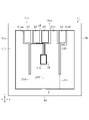
- FIG. 1 is a plan view of one embodiment of a semiconductor device.
- FIG. 2 is a plan view of the semiconductor device of FIG. 1 with the protective insulating film omitted.
- 3 is a plan view schematically showing the active region, peripheral region, and intermediate region of the semiconductor device of FIG. 2.
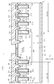
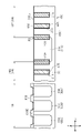
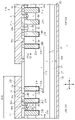
- FIG. 4 is a cross-sectional view schematically showing the cross-sectional structure of the semiconductor device of FIG. 1 taken along line 4-4.
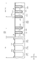
- FIG. 5 is a cross-sectional view schematically showing the cross-sectional structure of the semiconductor device of FIG. 1 taken along line 5-5.
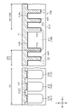
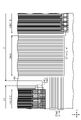
- FIG. 6 is a plan view showing the sense cell area and its periphery in the active area.
- FIG. 7 is an enlarged view of part of FIG. FIG.
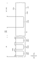
- FIG. 8 is a circuit diagram schematically showing part of the circuit configuration of the semiconductor device.
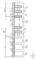
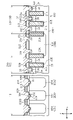
- FIG. 9 is an explanatory diagram for explaining an example of the manufacturing process of the method for manufacturing a semiconductor device.
- FIG. 10 is an explanatory diagram for explaining an example of the manufacturing process of the method for manufacturing a semiconductor device.
- FIG. 11 is an explanatory diagram for explaining an example of the manufacturing process of the method for manufacturing a semiconductor device.
- FIG. 12 is an explanatory diagram for explaining an example of the manufacturing process of the method for manufacturing a semiconductor device.
- FIG. 13 is an explanatory diagram for explaining an example of the manufacturing process of the method for manufacturing a semiconductor device.
- 14A and 14B are explanatory diagrams for explaining an example of a manufacturing process of a method for manufacturing a semiconductor device.
- FIG. 15A and 15B are explanatory diagrams for explaining an example of a manufacturing process of a method for manufacturing a semiconductor device.
- FIG. 16 is an explanatory diagram for explaining an example of the manufacturing process of the method for manufacturing a semiconductor device.
- 17A and 17B are explanatory diagrams for explaining an example of a manufacturing process of a method for manufacturing a semiconductor device.
- FIG. 18 is a cross-sectional view schematically showing cross-sectional structures of a main cell region and a sense cell region of an active region in a semiconductor device of a comparative example.
- FIG. 19 is an enlarged plan view of a portion of the sense cell region and its periphery in the semiconductor device of the modification.
- FIG. 20 is a cross-sectional view schematically showing the cross-sectional structure of part of the main cell region of the semiconductor device of the modification.
- Embodiments of the semiconductor device will be described below with reference to the drawings.
- the embodiments shown below are examples of configurations and methods for embodying technical ideas, and the materials, shapes, structures, layouts, dimensions, etc. of each component are not limited to the following. .
- FIG. 1 A schematic configuration of a semiconductor device 10 of the present embodiment will be described with reference to FIGS. 1 to 5.
- the semiconductor device 10 is a trench gate type IGBT (Insulated Gate Bipolar Transistor).
- IGBT Insulated Gate Bipolar Transistor
- This semiconductor device 10 is used, for example, as a switching element in an in-vehicle inverter device. In this case, a current of 5 A or more and 1000 A or less flows through the semiconductor device 10 .
- the semiconductor device 10 is formed, for example, in the shape of a rectangular flat plate.
- the semiconductor device 10 includes a main surface 10s, a rear surface 10r (see FIG. 4) facing away from the main surface 10s, and four side surfaces formed between the main surface 10s and the rear surface 10r. 10a to 10d.
- the device side surfaces 10a to 10d are surfaces connecting, for example, the device main surface 10s and the device rear surface 10r, and are perpendicular to both the device main surface 10s and the device rear surface 10r.
- 10 s of device main surfaces are formed in a square, for example.
- the length of one side of the device main surface 10s is about 11 mm. That is, the chip size of the semiconductor device 10 of this embodiment is 11 mm square. Note that the chip size of the semiconductor device 10 can be arbitrarily changed.
- the direction in which the main surface 10s and the rear surface 10r of the device face is referred to as the "z direction". It can also be said that the z direction is the height direction of the semiconductor device 10 .
- the two directions that are perpendicular to each other are defined as the "x-direction" and the "y-direction”.
- the device side surfaces 10a and 10b constitute both end surfaces of the semiconductor device 10 in the x direction
- the device side surfaces 10c and 10d constitute both end surfaces of the semiconductor device 10 in the y direction.
- FIG. 2 shows the electrode configuration of the semiconductor device 10.
- the semiconductor device 10 includes an emitter electrode 21, an anode electrode 22, a gate electrode 23, a current sense electrode 24, and a cathode electrode 25.
- the semiconductor device 10 also includes a temperature sensitive diode 60 for detecting the temperature of the semiconductor device 10 .
- the emitter electrode 21 corresponds to the "first electrode section” and the current sense electrode 24 corresponds to the "second electrode section”.
- the semiconductor device 10 also includes gate fingers 26 electrically connected to the gate electrodes 23 .
- the gate finger 26 is for rapidly supplying the current supplied to the gate electrode 23 also to the main cell in the portion of the emitter electrode 21 away from the gate electrode 23 .
- the semiconductor device 10 has a collector electrode 27 .
- the collector electrode 27 is formed over the entire surface of the back surface 10r of the device. 1 and 3, the gate fingers 26 are omitted for the sake of convenience.
- the emitter electrode 21 When viewed from the z-direction, the emitter electrode 21 is formed over most of the main surface 10s of the device.
- the cathode electrode 25, the anode electrode 22, the gate electrode 23, and the current sense electrode 24 are each arranged in the electrode placement region 10ce near the device side surface 10c among both ends in the y direction of the device main surface 10s.
- These electrodes 22 to 25 are aligned with each other in the y direction and spaced apart from each other in the x direction.
- the emitter electrode 21 has electrode accommodating portions 21aa and 21ab, a diode placement portion 21b, and a pair of gate finger accommodating portions 21d.
- the electrode accommodating portions 21aa and 21ab are provided at the ends of the emitter electrode 21 in the y direction that are closer to the device side surface 10c.
- the electrode accommodating portion 21aa is a portion that accommodates the cathode electrode 25, the anode electrode 22, and the gate electrode 23, and has a concave shape.
- the electrode accommodating portion 21ab is a portion that accommodates the current sense electrode 24 and has a concave shape.
- the electrode accommodating portion 21aa is arranged closer to the device side surface 10a than the electrode accommodating portion 21ab in the x direction.
- the cathode electrode 25, the anode electrode 22, the gate electrode 23, and the current sense electrode 24 housed in the electrode housing portions 21aa and 21ab are aligned in the y direction and spaced apart from each other in the x direction.
- the cathode electrode 25, the anode electrode 22, the gate electrode 23, and the current sense electrode 24 are arranged in the x direction from the device side surface 10a toward the device side surface 10b. , and the current sense electrode 24 .
- a portion of the emitter electrode 21 between the electrode accommodating portion 21aa and the electrode accommodating portion 21ab in the x direction constitutes an emitter sense region 21f that constitutes an emitter sense electrode pad 16, which will be described later.
- the emitter sense region 21f constitutes part of the electrode accommodating portion 21aa and part of the electrode accommodating portion 21ab. It can also be said that the emitter sense region 21f is formed between the gate electrode 23 and the current sense electrode 24 in the x direction.
- the diode arrangement portion 21b includes a portion where the temperature-sensitive diode 60 is arranged, and is connected to the electrode accommodation portion 21aa.
- the diode arrangement portion 21b is provided substantially at the center of the emitter electrode 21 in the x-direction and the y-direction. Therefore, it can be said that the temperature-sensitive diode 60 is arranged substantially in the center of the emitter electrode 21 in the x-direction and the y-direction. Further, as shown in FIG. 2, it can be said that the temperature sensitive diode 60 is arranged substantially in the center of the main surface 10s of the device in the x direction and the y direction.
- the diode arrangement portion 21b is a portion where the emitter electrode 21 is not formed. A portion of the diode arrangement portion 21b where the temperature-sensitive diode 60 is arranged is formed in a rectangular shape when viewed from the z direction. The emitter electrode 21 is formed so as to surround the temperature sensitive diode 60 in order to constitute the diode arrangement portion 21b.
- the diode arrangement portion 21b is connected to the electrode accommodation portion 21aa by extending in the y-direction from a portion of the diode arrangement portion 21b where the temperature-sensitive diode 60 is arranged to the electrode accommodation portion 21aa.
- a pair of gate finger housing portions 21d are arranged dispersedly on both sides of the diode arrangement portion 21b in the x direction.
- One gate finger accommodating portion 21d extends along the y direction from the electrode accommodating portion 21aa, and the other gate finger accommodating portion 21d extends along the y direction from the electrode accommodating portion 21ab.
- a part of the gate finger 26 is arranged in each gate finger accommodating portion 21d.
- Each gate finger accommodation portion 21d extends from the electrode accommodation portions 21aa and 21ab of the emitter electrode 21 along the y direction.
- the tip of each gate finger accommodating portion 21d is arranged closer to the electrode accommodating portions 21aa and 21ab than the end of the emitter electrode 21 in the y direction that is closer to the device side surface 10d.
- the gate finger 26 surrounds the emitter electrode 21 and extends both inside the pair of gate finger housing portions 21d and inside the diode arrangement portion 21b.
- the gate finger 26 in the diode arrangement portion 21b is formed so as to surround the temperature sensitive diode 60.
- the gate finger 26 has surface-side wiring and internal wiring connected to the surface-side wiring.
- the surface-side wiring is made of, for example, a metal material, and the internal wiring is made of, for example, polysilicon.
- the surface-side wiring is provided at positions aligned with the electrodes 21 to 25 in the z-direction.
- the internal wiring is arranged closer to the device back surface 10r than the metal wiring in the z-direction.
- a gate finger 26A is provided between the diode placement portion 21b and the pair of gate finger accommodating portions 21d and the end portion closer to the side surface 10d of the emitter electrode 21 in the y direction.
- the gate finger 26A is formed by internal wiring connected to the internal wiring of the gate finger 26A. That is, the gate fingers 26A do not have surface-side wiring. Therefore, the gate finger 26A is arranged closer to the device rear surface 10r than the emitter electrode 21 at the position overlapping the emitter electrode 21 when viewed in the z direction.
- a protective insulating film 17 is provided on the main surface 10s of the device so as to cover the electrodes 21-25.
- Protective insulating film 17 is an organic protective film that protects semiconductor device 10 from the outside of semiconductor device 10, and is formed of a material containing polyimide (PI), for example.
- PI polyimide
- the protective insulating film 17 is provided with first to sixth openings 17A to 17F that expose the electrodes 21 to 25, respectively.
- the electrodes 21 to 25 exposed by the first to sixth openings 17A to 17F constitute pads to which conductive members from the outside of the semiconductor device 10 are joined. Such pads include emitter electrode pad 11 , cathode electrode pad 12 , anode electrode pad 13 , gate electrode pad 14 , current sense electrode pad 15 and emitter sense electrode pad 16 .
- the first to sixth openings 17A to 17F provided in the protective insulating film 17 are spaced apart from each other when viewed in the z direction.
- the emitter electrode pad 11 is a portion of the emitter electrode 21 exposed from the first opening 17A, and constitutes the emitter of the IGBT.
- the first opening 17A opens most of the emitter electrode 21 .
- Most of the first opening 17A opens a portion of the emitter electrode 21 closer to the device side surface 10d than the electrode accommodating portions 21aa and 21ab.
- the protective insulating film 17 is provided at a position overlapping the pair of gate finger accommodating portions 21d and at a position overlapping the diode placement portion 21b and the gate finger 26A when viewed in the z direction.
- the cathode electrode pad 12 is a portion of the emitter electrode 21 exposed from the second opening 17B, and constitutes the cathode of the temperature sensitive diode 60 .
- the second opening 17B opens the end of the emitter electrode 21 near the device side surface 10a and the device side surface 10c.
- the second opening 17B opens a portion of the emitter electrode 21 adjacent to the anode electrode 22 with a gap in the x direction.
- the second opening 17B is provided at a position adjacent to and spaced from the first opening 17A in both the x direction and the y direction. That is, it can be said that the cathode electrode pad 12 is provided at a position adjacent to the emitter electrode pad 11 with a space therebetween in the y direction.
- the cathode electrode pad 12 is arranged closer to the device side surface 10c than the center of the device main surface 10s in the y direction.
- the cathode electrode pad 12 is adjacent to the anode electrode 22 in the x direction.
- the cathode electrode pad 12 and the anode electrode 22 are arranged side by side along the device side surface 10c when viewed from the z direction.
- the anode electrode pad 13 is a portion of the anode electrode 22 exposed from the third opening 17C and constitutes the anode of the temperature sensitive diode 60 .
- the third opening 17C is formed in a rectangular shape that is one size smaller than the anode electrode 22 when viewed from the z direction.
- the gate electrode pad 14 is a portion of the gate electrode 23 exposed from the fourth opening 17D, and constitutes the gate of the IGBT.
- the fourth opening 17D is formed in a rectangular shape that is one size smaller than the gate electrode 23 when viewed from the z direction.
- the current sense electrode pad 15 is a portion of the current sense electrode 24 exposed from the fifth opening 17E, and constitutes a terminal for extracting information for detecting current flowing through the IGBT to the outside.
- the fifth opening 17E is formed in a rectangular shape that is one size smaller than the current sense electrode 24 when viewed from the z direction.
- the emitter sense electrode pad 16 is a portion of the emitter electrode 21 exposed from the sixth opening 17F.
- the sixth opening 17F is formed in a rectangular shape that is one size smaller than the emitter sense region 21f when viewed in the z direction.
- part of the gate finger 26 extends from the gate electrode 23 toward the device side surface 10a and the device side surface 10d. More specifically, a part of the gate finger 26 detours from the gate electrode 23 closer to the device side surface 10c than the anode electrode 22, and forms a gate finger accommodating portion closer to the device side surface 10a than the temperature sensitive diode 60 in the y direction. It extends towards 21d. Another portion of gate finger 26 extends from gate electrode 23 toward device side 10b and device side 10d. More specifically, another portion of the gate finger 26 bypasses the gate electrode 23 closer to the device side 10c than the emitter sense region 21f to the gate closer to the device side 10b than the temperature sensitive diode 60 in the y-direction. It extends toward the finger accommodating portion 21d.
- the semiconductor device 10 includes an active region 18, a peripheral region 19 surrounding the active region 18, and an intermediate region 20 surrounded by the main cell region 18M and the peripheral region 19 when viewed from the z direction. , is equipped with The active region 18, the outer peripheral region 19, and the intermediate region 20 are regions defined when a semiconductor substrate 30 (described later) of the semiconductor device 10 is viewed from the z direction.
- the active region 18 is a region in which transistors are formed.
- the active region 18 is formed over most of the main surface 10s of the device.
- the active region 18 has a main cell region 18M formed with a main cell 18A (see FIG. 4) and a sense cell region 24A formed with a sense cell 24B.
- the sense cell region 24A is formed at a position separated from the main cell region 18M.
- the main cell region 18M is a region through which the main current flows.
- a main current is a current that flows from the collector electrode 27 toward the emitter electrode 21 .
- the active region 18 is formed in a region overlapping the emitter electrode 21 when viewed from the z direction. In other words, emitter electrode 21 covers active area 18 .
- the main cell region 18M does not overlap the gate finger 26A (see FIG. 2) in the z-direction even though it overlaps the emitter electrode 21. As shown in FIG.
- the sense cell region 24A is a region through which a sense current corresponding to the main current flows.
- the sense cell region 24A is formed between the intermediate region 20 and the main cell region 18M in the y direction. More specifically, the sense cell region 24A is formed between the region of the intermediate region 20 that overlaps the current sense electrode 24 and the main cell region 18M that faces this region in the y direction.
- the sense current is a current corresponding to the area ratio of the main cell region 18M and the sense cell region 24A with respect to the main current. As shown in FIG. 3, the area of the sense cell region 24A is sufficiently smaller than that of the main cell region 18M. That is, a sense current sufficiently smaller than the main current flows through the sense cell region 24A.
- the sense cell region 24A is formed in a region overlapping with the current sense electrode 24 when viewed from the z direction. As shown in FIG. 1, the sense cell region 24A is formed at a position different from the fifth opening 17E. That is, the sense cell region 24A is covered with the protective insulating film 17. As shown in FIG.
- the outer peripheral region 19 is a region where a termination structure for improving the withstand voltage of the semiconductor device 10 is provided.
- the peripheral region 19 is a region surrounding the emitter electrode 21 excluding the regions where the electrodes 22 to 25 are formed. No main cells 18A are formed in the peripheral region 19 .
- the peripheral region 19 is a region outside the emitter electrode 21 .
- the intermediate region 20 is a region that overlaps with the cathode electrode 25, the anode electrode 22, the gate electrode 23, and the current sense electrode 24 when viewed from the z direction.
- cathode electrode 25 , anode electrode 22 , gate electrode 23 and current sense electrode 24 each cover intermediate region 20 .
- Intermediate region 20 includes a region outside main cell region 18M and sense cell region 24A, in other words, a region where main cell 18A and sense cell 24B are not formed.
- FIG. 4 is a cross-sectional view showing the cross-sectional structure of the semiconductor device 10 taken along line 4-4 of FIG. 1, and schematically shows an example of the cross-sectional structure of the semiconductor device 10 in the main cell region 18M and the sense cell region 24A. Note that the protective insulating film 17 is omitted in FIG. 4 for the sake of convenience.
- the semiconductor device 10 has a semiconductor substrate 30 .
- Semiconductor substrate 30 is made of a material containing, for example, n ⁇ -type Si (silicon).
- Semiconductor substrate 30 has a thickness of, for example, 50 ⁇ m or more and 200 ⁇ m or less.
- the semiconductor substrate 30 has a substrate front surface 30s and a substrate rear surface 30r facing opposite sides in the z-direction.
- the z direction can also be said to be the thickness direction of the semiconductor substrate 30 .
- the semiconductor substrate 30 has a structure in which a p + -type collector layer 31, an n-type buffer layer 32, and an n ⁇ -type drift layer 33 are laminated in order from the substrate back surface 30r toward the substrate surface 30s. . Therefore, the collector layer 31, the buffer layer 32, and the drift layer 33 are provided in common to the main cell region 18M and the sense cell region 24A.
- a collector electrode 27 is formed on the substrate rear surface 30r. The collector electrode 27 is formed over substantially the entire surface of the substrate rear surface 30r.
- the surface of the collector electrode 27 opposite to the collector layer 31 constitutes the back surface 10 r of the semiconductor device 10 .
- the z direction corresponds to the thickness direction of the drift layer 33 . Therefore, "viewed from the z-direction" has the same meaning as "viewed from the thickness direction of the drift layer”.
- collector layer 31 As the p-type impurity of collector layer 31, for example, B (boron), Al (aluminum), or the like is used.
- the impurity concentration of collector layer 31 is, for example, 1 ⁇ 10 15 cm ⁇ 3 or more and 2 ⁇ 10 19 cm ⁇ 3 or less.
- n-type impurities for buffer layer 32 and drift layer 33 for example, N (nitrogen), P (phosphorus), As (arsenic), or the like is used.
- the impurity concentration of buffer layer 32 is, for example, 1 ⁇ 10 15 cm ⁇ 3 or more and 5 ⁇ 10 17 cm ⁇ 3 or less.
- the impurity concentration of drift layer 33 is lower than that of buffer layer 32, and is, for example, 1 ⁇ 10 13 cm ⁇ 3 or more and 5 ⁇ 10 14 cm ⁇ 3 or less.
- a p-type base region 34 is formed on the surface of the drift layer 33, that is, the substrate surface 30s.
- the base region 34 is formed over substantially the entire surface of both the main cell region 18M and the sense cell region 24A.
- the impurity concentration of base region 34 is, for example, 1 ⁇ 10 16 cm ⁇ 3 or more and 1 ⁇ 10 18 cm ⁇ 3 or less.
- the depth of base region 34 from substrate surface 30s is, for example, 1.0 ⁇ m or more and 4.0 ⁇ m or less.
- the base region 34 corresponds to the "second conductivity type body layer".
- a plurality of trenches 35 are arranged side by side on the surface (substrate surface 30s) of the base region 34 in both the main cell region 18M and the sense cell region 24A.
- Each trench 35 extends, for example, along the y direction and is arranged apart from each other in the x direction.
- the main cell region 18M is partitioned into striped main cells 18A
- the sense cell region 24A is partitioned into striped sense cells 24B.
- the distance between adjacent trenches 35 in the x direction is, for example, 1.5 ⁇ m or more and 7.0 ⁇ m or less.
- each trench 35 (x-direction dimension of the trench 35) is, for example, 0.5 ⁇ m or more and 3.0 ⁇ m or less.
- Each trench 35 penetrates the base region 34 in the z-direction and extends halfway through the drift layer 33 .
- the trenches 35 in the main cell region 18M may be formed in a grid pattern so as to partition the matrix-shaped main cells 18A.
- each trench 35 in the sense cell region 24A may be formed in a grid pattern so as to partition the matrix-shaped sense cells 24B.
- n + -type emitter region 36 is formed on the surface (substrate surface 30s) of the base region 34 in both the main cell region 18M and the sense cell region 24A.
- the emitter regions 36 are arranged on both sides of the trench 35 in the x direction. That is, it can be said that the emitter regions 36 are provided on both sides of the trenches 35 in the arrangement direction of the trenches 35 in the base region 34 . Therefore, two emitter regions 36 are spaced apart from each other in the x direction between the trenches 35 adjacent to each other in the x direction.
- the depth of each emitter region 36 is, for example, 0.2 ⁇ m or more and 0.6 ⁇ m or less.
- the impurity concentration of each emitter region 36 is higher than that of the base region 34, and is, for example, 1 ⁇ 10 19 cm ⁇ 3 or more and 5 ⁇ 10 20 cm ⁇ 3 or less.
- a p + -type base contact region 37 is formed on the surface (substrate surface 30s) of the base region 34 in both the main cell region 18M and the sense cell region 24A.
- the base contact region 37 is provided at a position adjacent to the emitter region 36 in the x direction. That is, the base contact region 37 is provided between two emitter regions 36 provided between trenches 35 adjacent in the x direction in the x direction.
- Each base contact region 37 may be formed deeper than the emitter region 36 .
- the depth of each base contact region 37 is, for example, 0.2 ⁇ m or more and 1.6 ⁇ m or less.
- the impurity concentration of each base contact region 37 is higher than that of the base region 34, for example, 5 ⁇ 10 18 cm ⁇ 3 or more and 1 ⁇ 10 20 cm ⁇ 3 or less.
- Insulating film 38 is integrally formed on both the inner surface of each trench 35 and the substrate surface 30s.
- Insulating film 38 contains, for example, silicon oxide (SiO 2 ).
- the thickness of insulating film 38 is, for example, 1100 ⁇ or more and 1300 ⁇ or less.
- the insulating film 38 is formed to cover both the main cell region 18M and the sense cell region 24A.
- An electrode material containing, for example, polysilicon or the like is embedded in each trench 35 with an insulating film 38 interposed therebetween.
- the electrode material embedded in each trench 35 is electrically connected to either the gate electrode 23 (gate finger 26 ) or the emitter electrode 21 . That is, the electrode material embedded in each trench 35 forms the gate trench 23A and the emitter trench 21A.
- the arrangement of the gate trenches 23A and the emitter trenches 21A in the arrangement direction of the plurality of trenches 35 is the same.
- the plurality of trenches 35 are arranged in the arrangement direction of the gate trenches 23A, the emitter trenches 21A, the emitter trenches 21A, the emitter trenches 21A, and the gate trenches 23A. Five trenches are repeatedly arranged in the arrangement direction.
- both the gate trench 23A and the emitter trench 21A are buried up to the opening end of each trench 35. As shown in FIG. Thus, a plurality of main cells 18A are formed in the main cell region 18M, and a plurality of sense cells 24B are formed in the sense cell region 24A.
- An intermediate insulating film 39 is formed on the surface 38s of the insulating film 38 provided on the substrate surface 30s.
- Intermediate insulating film 39 contains, for example, SiO 2 .
- a barrier layer 40 is formed on the surface 39s of the intermediate insulating film 39 to prevent the intermediate insulating film 39 from being charged by external ions.
- the barrier layer 40 is made of a material having a smaller diffusion coefficient than the protective insulating film 17 , the insulating film 38 and the intermediate insulating film 39 .
- Barrier layer 40 is made of a material containing, for example, silicon nitride (SiN).
- An emitter electrode 21 is formed on the surface 40 s of the barrier layer 40 .
- the intermediate insulating film 39 is an interlayer insulating film that fills the space between the emitter electrode 21 and the gate trench 23A.
- the thickness of the intermediate insulating film 39 is thicker than the thickness of the insulating film 38 .
- the thickness of the intermediate insulating film 39 is thicker than the thickness of the barrier layer 40 .
- the thickness of intermediate insulating film 39 is, for example, 3000 ⁇ or more and 15000 ⁇ or less.
- the portion covering the main cell region 18M corresponds to the "first insulating film”
- the portion covering the sense cell region 24A corresponds to the "first insulating film”. 2 insulating film”.
- both the first insulating film and the second insulating film are composed of the laminated structure of the insulating film 38, the intermediate insulating film 39, and the barrier layer 40 in this embodiment.
- a plurality of contact holes 39a and 39b are provided in the laminated structure of the insulating film 38, the intermediate insulating film 39, and the barrier layer 40 so as to pass through the insulating film 38, the intermediate insulating film 39, and the barrier layer 40 in the z direction, respectively.
- the contact hole 39a is an opening provided in the laminated structure of the insulating film 38, the intermediate insulating film 39, and the barrier layer 40 covering the main cell region 18M. It is located in a position overlapping with the Thereby, the base contact region 37 is exposed from the laminated structure of the insulating film 38 , the intermediate insulating film 39 and the barrier layer 40 .
- the emitter electrode 21 is formed on the surface 40s of the barrier layer 40 and connected to the base contact region 37 through the contact hole 39a.
- the contact hole 39b is an opening provided in the laminated structure of the insulating film 38 covering the sense cell region 24A, the intermediate insulating film 39, and the barrier layer 40, and is located between the base contact region 37 of the sense cell region 24A and the base contact region 37 of the sense cell region 24A when viewed from the z direction. placed in an overlapping position. Thereby, the base contact region 37 is exposed from the laminated structure of the insulating film 38 , the intermediate insulating film 39 and the barrier layer 40 .
- the current sense electrode 24 is formed on the surface 40s of the barrier layer 40 and connected to the base contact region 37 through the contact hole 39b.
- the emitter electrode 21 has a layered structure of a barrier metal layer and a metal wiring layer formed on the barrier metal layer.
- the barrier metal layer is made of a material containing TiN (titanium nitride), for example.
- the metal wiring layer is made of a material containing, for example, AlCu (alloy of aluminum and copper).
- the emitter electrode 21 has a contact 21m embedded in the contact hole 39a and a laminated electrode portion 21n laminated on the barrier layer 40. As shown in FIG. The contact 21m and the laminated electrode portion 21n are integrated. Both the contact 21m and the laminated electrode portion 21n are formed of a laminated structure of a barrier metal layer and a metal wiring layer.
- the contact hole 39a corresponds to the "main side opening"
- the contact hole 39b corresponds to the "sense side opening".
- the current sense electrode 24 is electrically connected to the sense cell 24B in the sense cell region 24A.
- the sense cell region 24A is formed at a position overlapping the current sense electrode 24 when viewed in the z direction.
- the current sense electrode 24 has the same configuration as the emitter electrode 21, and has a laminated structure of a barrier metal layer and a metal wiring layer. Further, the current sense electrode 24 has a contact 24C in which a part of the current sense electrode 24 enters the contact hole 39b, similarly to the emitter electrode 21. As shown in FIG. Contact 24C is in contact with base contact region 37 of sense cell region 24A.
- the current sense electrodes 24 are electrically connected to an external integrated circuit (IC) by wires, for example.
- IC integrated circuit
- This integrated circuit is connected to a microcomputer, for example through a shunt resistor, and senses the current generated in the sense cell area 24A.
- the magnitude of the main current flowing through the main cell 18A is detected by multiplying the magnitude of the sensed current by the area ratio of the sense cell region 24A and the main cell region 18M.
- the operation of the semiconductor device 10 is stopped to protect the semiconductor device 10 from damage due to overcurrent.
- FIG. 5 shows a cross-sectional structure of part of the outer peripheral region 19 .
- the outer peripheral region 19 is provided with a gate finger 26 , an emitter lead-out portion 41 , an FLR (Field Limiting Ring) portion 42 , and an equipotential ring 43 .
- the gate finger 26, the emitter lead-out portion 41, and the equipotential ring 43 are each made up of a laminated structure of barrier metal layers and metal wiring layers, which have the same configuration as the emitter electrode 21.
- FIG. 5 shows a cross-sectional structure of part of the outer peripheral region 19 .
- the outer peripheral region 19 is provided with a gate finger 26 , an emitter lead-out portion 41 , an FLR (Field Limiting Ring) portion 42 , and an equipotential ring 43 .
- the gate finger 26, the emitter lead-out portion 41, and the equipotential ring 43 are each made up of a laminated structure of barrier metal layers and metal wiring layers, which have the same configuration as the emit
- a p-type well region 34A which is a semiconductor region of the second conductivity type, is formed in a region adjacent to the main cell region 18M in the peripheral region 19.
- Well region 34A is formed, for example, to surround main cell region 18M.
- the well region 34A is formed closer to the substrate rear surface 30r than the trench 35 of the main cell region 18M. Therefore, the well region 34A is formed closer to the substrate rear surface 30r than the base region 34 of the main cell region 18M.
- the impurity concentration of well region 34A is lower than that of base region 34 .
- a gate finger 26 and an emitter lead-out portion 41 are formed at positions overlapping with the well region 34A when viewed in the z-direction.
- the emitter lead-out portion 41 is arranged outside the gate fingers 26 .
- the emitter lead-out portion 41 is a portion integrated with the emitter electrode 21 and is formed in an annular shape so as to surround the gate finger 26 .
- the FLR section 42 is a termination structure for improving the breakdown voltage of the semiconductor device 10 and is provided outside the emitter routing section 41 .
- the FLR portion 42 is formed in an annular shape surrounding the emitter electrode 21 and the electrodes 22-24. In this embodiment, the FLR portion 42 is formed in a closed annular shape.
- the FLR portion 42 has a function of improving the breakdown voltage of the semiconductor device 10 by alleviating the electric field in the outer peripheral region 19 and suppressing the influence of external ions.
- the FLR section 42 is composed of a plurality (four in this embodiment) of annular conductors and semiconductor regions spaced apart from each other.
- a substrate surface 30s of the semiconductor substrate 30 is formed with a plurality of (four in this embodiment) annular guard rings 42a to 42d.
- the guard rings 42a to 42d are formed in a closed annular shape when viewed from the z direction.
- Guard rings 42 a - 42 d are partially formed in drift layer 33 .
- the guard rings 42a to 42d are semiconductor regions of the second conductivity type (p-type in this embodiment), and are spaced apart from each other in the direction perpendicular to the z-direction.
- Guard rings 42a to 42d are arranged in the order of guard ring 42a, guard ring 42b, guard ring 42c, and guard ring 42d in the direction away from emitter electrode 21.
- FIG. The width Wge of the outermost guard ring 42d is greater than the widths Wg of the other guard rings 42a-42c.
- B, Al, or the like, for example, is used as the p-type impurity for each of the guard rings 42a-42d.
- the impurity concentration of guard rings 42a-42d is, for example, the same as that of base region 34, and is, for example, 1 ⁇ 10 16 cm ⁇ 3 or more and 1 ⁇ 10 18 cm ⁇ 3 or less. Therefore, the impurity concentration of the guard rings 42a-42d is higher than that of the well region 34A. In other words, the impurity concentration of well region 34A is lower than that of guard rings 42a-42d.
- the FLR section 42 has field plates 42e-42h provided corresponding to the guard rings 42a-42d.
- the field plate 42e is provided at a position overlapping the guard ring 42a
- the field plate 42f is provided at a position overlapping the guard ring 42b
- the field plate 42g is provided at a position overlapping the guard ring 42c
- the field plate 42f is provided at a position overlapping the guard ring 42b.
- 42h is provided at a position overlapping the guard ring 42d.
- Field plate 42e contacts guard ring 42a
- field plate 42f contacts guard ring 42b
- field plate 42g contacts guard ring 42c
- field plate 42h contacts guard ring 42d.
- the field plates 42e to 42h are formed in a closed annular shape when viewed from the z direction.
- the equipotential ring 43 is a termination structure for improving the breakdown voltage of the semiconductor device 10 and is formed in a ring so as to surround the FLR section 42 .
- the equipotential ring 43 is formed on the outer periphery of the outer peripheral region 19 .
- the equipotential ring 43 is formed to have a closed annular shape when viewed from the z direction.
- the equipotential ring 43 has a function of improving the withstand voltage of the semiconductor device 10 .
- the equipotential ring 43 consists of a channel stop region of the first conductivity type (n + type) formed on the surface of the drift layer 33 (substrate surface 30s) and internal wirings provided in the insulating film 38 and the intermediate insulating film 39. and surface-side wiring provided on the surface 40 s of the barrier layer 40 .
- the surface-side wiring is electrically connected to the internal wiring through an opening penetrating the intermediate insulating film 39 .
- the surface-side wiring is electrically connected to the channel stop region through an opening penetrating both the intermediate insulating film 39 and the insulating film 38 .
- the protective insulating film 17 includes a portion of the emitter electrode 21, a portion of each of the electrodes 22 to 25, the gate finger 26, the emitter lead-out portion 41, the FLR portion 42, and the equipotential portion of the semiconductor device 10. It covers the ring 43.
- FIG. 6 shows an enlarged plan view of the end portion of the current sense electrode 24 closer to the side surface 10d of the y-direction ends, and FIG. An enlarged view of the periphery is shown.
- a sense cell region 24A in which the main cell 18A (see FIG. 4) is formed is formed in the region RIS of the semiconductor substrate 30 in the region RIS of the semiconductor substrate 30, a sense cell region 24A in which the main cell 18A (see FIG. 4) is formed is formed.
- the sense cell region 24A is formed at one of both ends of the region RIS in the y direction, which is closer to the device side surface 10d (see FIG. 2).
- a well region 34A is formed in a region of the region RIS in the semiconductor substrate 30 other than the sense cell region 24A. That is, the sense cell 24B (see FIG. 4) is not formed in the region RIS other than the sense cell region 24A.
- a plurality of sense cells 24B are arranged in the y direction in the sense cell region 24A.
- the sense cell 24B has the same configuration as the main cell 18A (see FIG. 5).
- a plurality of sense cells 24B are provided to extend in the x direction. Therefore, it can be said that a plurality of trenches 35 extending in the x-direction are arranged side by side at intervals in the y-direction. These trenches 35 are connected every predetermined number of trenches 35 at both ends in the x direction.
- a well region 34A is formed between the sense cell region 24A and the main cell region 18M in the y direction. More specifically, as shown in FIG. 4, the well region 34A includes a first trench 35E closest to the sense cell region 24A among the plurality of trenches 35 in the main cell region 18M and It is formed between the second trench 35S closest to the main cell region 18M.
- the well region 34A is formed closer to the substrate rear surface 30r than the first trench 35E and the second trench 35S. That is, in the depth direction of each trench 35E, 35S, the well region 34A is formed deeper than the bottom 35b of each trench 35E, 35S. In other words, the well region 34A is formed closer to the drift layer 33 than the bottoms 35b of the trenches 35E and 35S.
- the first trench 35E is the trench 35 provided in the main cell region 18M, but is a trench different from the trench 35 forming the main cell 18A.
- the second trench 35S is the trench 35 provided in the sense cell region 24A, but is a trench different from the trench 35 forming the sense cell 24B.
- the impurity concentration of the well region 34A is lower than that of the guard rings 42a-42d. Therefore, it can be said that the impurity concentration of the well region 34A is lower than that of both the guard rings 42a to 42d and the base region 34.
- the electrode material embedded in the first trench 35E forms the gate trench 23A
- the electrode material embedded in the second trench 35S forms the gate trench 23A.
- the trenches 35 at the outer edges of both the main cell region 18M and the sense cell region 24A serve as the gate trenches 23A.
- At least one of the first trench 35E and the second trench 35S may be configured by the emitter trench 21A. That is, the trenches 35 at the outer edges of both the main cell region 18M and the sense cell region 24A may serve as the emitter trenches 21A.
- the well region 34A is formed at a position overlapping the trenches 35E and 35S when viewed from the z-direction. Further, when viewed from the z-direction, the well region 34A does not protrude toward the main cell region 18M from the first trenches 35E in the y-direction. Further, when viewed from the z direction, the well region 34A does not protrude toward the sense cell region 24A from the second trench 35S in the y direction. Thus, the well region 34A is formed to partially cover the bottoms 35b of the trenches 35E and 35S.
- the emitter electrode 21 extends toward the sense cell region 24A beyond the first trenches 35E of the main cell region 18M.
- the current sense electrode 24 extends toward the main cell region 18M from the second trench 35S of the sense cell region 24A.
- the emitter electrode 21 and the current sense electrode 24 are arranged apart from each other in the y direction.
- the well region 34A has a portion overlapping the current sense electrode 24 and a portion overlapping the emitter electrode 21 when viewed from the z-direction. That is, the well region 34A has portions overlapping both the current sense electrode 24 and the emitter electrode 21 when viewed in the z direction. That is, when viewed from the z-direction, the emitter electrode 21 has a portion that protrudes closer to the sense cell region 24A than the main cell region 18M in the y-direction. When viewed from the z-direction, the current sense electrode 24 has a portion that protrudes closer to the main cell region 18M than the sense cell region 24A in the y-direction.
- a main cell region 18M is formed at a position facing the sense cell region 24A in the y direction via the well region 34A. More specifically, as shown in FIG. 6, the main cell region 18M is formed so as to surround the sense cell region 24A from three device side surfaces 10a, 10b and 10d (both of which are shown in FIG. 2).
- a well region 34A is formed between the sense cell region 24A and the main cell region 18M. Since the well region 34A is also formed in a portion overlapping with the current sense electrode 24, the well region 34A is formed so as to surround the sense cell region 24A when viewed from the z direction.
- a plurality of trenches 35 are provided in each of the contacts 24C and the sense cell regions 24A.
- trenches 35 in contact 24C and sense cell region 24A each extend in the x-direction.
- the trenches 35 in the contacts 24C and the sense cell regions 24A are alternately arranged in the y-direction.
- the semiconductor device 10 includes end contacts 24CE provided on both sides of the current sense electrode 24 in the y direction.
- the end contact 24CE is provided at a position separated from the sense cell region 24A. More specifically, the end contact 24CE is arranged between the sense cell region 24A and the main cell region 18M in the y-direction. When viewed from the z-direction, the end contact 24CE is arranged at a position overlapping a region of the well region 34A adjacent to the sense cell region 24A in the y-direction. End contact 24CE extends in the x-direction like contact 24C. In this embodiment, the x-direction length of the end contact 24CE is equal to the x-direction length of the contact 24C.
- the end contact 24CE corresponds to the "sense end contact".
- the distance between the end contact 24CE and the contact 24C adjacent to the end contact 24CE in the y direction is equal to the distance between the contacts 24C adjacent in the y direction among the plurality of contacts 24C.
- two end contacts 24CE are provided in the well region 34A at positions overlapping regions adjacent to the sense cell region 24A in the y direction. Note that FIG. 6 shows a structure in which one end contact 24CE is provided for ease of understanding of the drawing.
- a contact 21m for the emitter electrode 21 is arranged in the well region 34A. That is, the emitter electrode 21 is electrically connected to the well region 34A by the contact 21m.
- the contact 21m is provided at a position overlapping both the well region 34A and the emitter electrode 21 when viewed in the z direction.
- the emitter electrode 21 is provided with a plurality of contacts 21m.
- the contacts 21m of the emitter electrode 21 outside the main cell region 18M and arranged in the well region 34A are referred to as "first contact 21ma,” “second contact 21mb,” “third contact 21mc,” and “fourth contact 21m.” 21md” and “fifth contact 21me”.
- these contacts 21ma, 21mb, 21mc, 21md, and 21me correspond to "main contacts”.
- the first contact 21ma is arranged in the well region 34A between the sense cell region 24A and the main cell region 18M in the y direction.
- the first contact 21ma is arranged closer to the sense cell region 24A than the main cell region 18M.
- the first contact 21ma extends in the x direction. That is, the first contact 21ma extends parallel to the end contact 24CE. It can be said that the first contact 21ma extends parallel to both the trench 35 (see FIG. 4) of the sense cell region 24A and the trench 35 of the main cell region 18M. It can be said that the first contact 21ma extends along the long side direction of the rectangular sense cell region 24A when viewed from the z direction.
- the length of the first contact 21ma in the x direction is longer than the length of the end contact 24CE in the x direction.
- the length of the first contact 21ma in the x direction is longer than the length of the sense cell region 24A in the x direction.
- a plurality of first contacts 21ma are provided.
- the plurality of first contacts 21ma are arranged apart from each other in the y direction.
- the first contact 21ma is provided at a position facing the end contact 24CE in the y direction when viewed from the z direction.
- the number of first contacts 21ma is greater than the number of end contacts 24CE.
- the first contact 21ma corresponds to the "main end contact”.
- the second contact 21mb and the third contact 21mc are respectively arranged in the well region 34A between the sense cell region 24A and the main cell region 18M in the x direction.
- Second contact 21mb is arranged closer to device side surface 10a (see FIG. 1) than sense cell region 24A
- third contact 21mc is arranged closer to device side surface 10b (see FIG. 1) than sense cell region 24A.
- Each of second contact 21mb and third contact 21mc is arranged closer to sense cell region 24A than main cell region 18M.
- Each of second contact 21mb and third contact 21mc extends in the y direction. That is, both the second contact 21mb and the third contact 21mc extend in a direction perpendicular to the end contact 24CE.
- both the second contact 21mb and the third contact 21mc extend parallel to both the trench 35 (see FIG. 4) of the sense cell region 24A and the trench 35 of the main cell region 18M.
- both the second contact 21mb and the third contact 21mc can be said to extend along the short side direction of the rectangular sense cell region 24A when viewed from the z direction.
- the y-direction length of the second contact 21mb and the y-direction length of the third contact 21mc are equal to each other.
- the y-direction length of the second contact 21mb and the y-direction length of the third contact 21mc are each shorter than the x-direction length of the first contact 21ma.
- a plurality of second contacts 21mb are provided.
- the plurality of second contacts 21mb are arranged apart from each other in the x direction.
- a plurality of third contacts 21mc are provided.
- the plurality of third contacts 21mc are arranged apart from each other in the x direction.
- the number of second contacts 21mb is greater than the number of end contacts 24CE.
- the number of third contacts 21mc is greater than the number of end contacts 24CE.
- the fourth contact 21md and the fifth contact 21me are arranged on the opposite side of the sense cell region 24A from the main cell region 18M in the y direction.
- the fourth contact 21md and the fifth contact 21me are aligned in the y direction and spaced apart in the x direction.
- the fourth contact 21md and the fifth contact 21me each extend in the x direction. That is, both the fourth contact 21md and the fifth contact 21me extend parallel to the end contact 24CE. It can also be said that both the fourth contact 21md and the fifth contact 21me extend parallel to both the trench 35 (see FIG. 4) of the sense cell region 24A and the trench 35 of the main cell region 18M. It can be said that both the fourth contact 21md and the fifth contact 21me extend along the long side direction of the rectangular sense cell region 24A when viewed from the z direction.
- a plurality of fourth contacts 21md and a plurality of fifth contacts 21me are provided.
- the plurality of fourth contacts 21md are arranged apart from each other in the y direction.
- the plurality of fifth contacts 21me are arranged apart from each other in the y direction.
- the number of fourth contacts 21md is greater than the number of end contacts 24CE.
- the number of fifth contacts 21me is greater than the number of end contacts 24CE.
- the first to fifth contacts 21ma to 21me are arranged to surround the sense cell region 24A. That is, the emitter electrode 21 is formed so as to surround the sense cell region 24A. A portion of the emitter electrode 21 surrounding the sense cell region 24A has an open annular shape with a gap between the fourth contact 21md and the fifth contact 21me in the x direction when viewed from the z direction.
- the current sense electrode 24 extends to a position overlapping the sense cell region 24A through a gap formed between the fourth contact 21md and the fifth contact 21me in the emitter electrode 21 in the x direction.
- the end contact 24CE of the current sense electrode 24 and the first contact 21ma of the emitter electrode 21 are each connected to the well region 34A. That is, the current sense electrode 24 and the emitter electrode 21 are electrically connected via the well region 34A. Therefore, as shown in FIG. 4, the emitter electrode 21 and the current sense electrode 24 are electrically connected to each other through the resistance component of the well region 34A.
- the second contact 21mb, third contact 21mc, fourth contact 21md, and fifth contact 21me of the emitter electrode 21 are also connected to the well region 34A. Emitter electrode 21 is electrically connected to current sense electrode 24 via 34A.
- the sense IGBT 24S composed of the sense cells 24B in the sense cell region 24A is connected in parallel with the main IGBT 21M composed of the main cells 18A in the main cell region 18M. Both the gate of sense IGBT 24S and the gate of main IGBT 21M are electrically connected to gate electrode 23 .
- FIGS. 9 to 17 show a simplified configuration of the semiconductor device 10 showing the manufacturing process. Therefore, the shapes of the components of the semiconductor device 10 shown in FIGS. 9 to 17 may differ from the shapes of the components of the semiconductor device 10 shown in FIGS.
- FIGS. 9 to 17 show manufacturing processes of a portion of the main cell region 18M and the sense cell region 24A, and a portion of the FLR section 42, respectively.
- the manufacturing method of one semiconductor device 10 will be described with reference to FIGS.
- the method for manufacturing the semiconductor device 10 of the present embodiment is not limited to manufacturing one semiconductor device 10, and may be manufacturing a plurality of semiconductor devices 10.
- FIG. 9. 9 to 17 show a simplified configuration of the semiconductor device 10 showing the manufacturing process. Therefore, the shapes of the components of the semiconductor device 10 shown in FIGS. 9 to 17 may differ from the shapes of the components of the semiconductor device 10 shown in FIGS.
- FIGS. 9 to 17 show manufacturing processes of a portion of the main cell region 18M and the sense cell region 24A, and a portion of the
- the method for manufacturing the semiconductor device 10 of this embodiment includes a step of preparing a semiconductor substrate 830 made of a material containing Si.
- the semiconductor substrate 830 has an n ⁇ type drift layer 33 as a first conductivity type semiconductor layer.
- Drift layer 33 is formed over the entire semiconductor substrate 830 . That is, it can be said that the drift layer 33 is formed in both the main cell region 18M and the sense cell region 24A.
- the semiconductor substrate 830 has a substrate front surface 830s and a substrate rear surface 830r facing opposite sides in the thickness direction (z direction). Therefore, it can be said that the substrate surface 830 s is the surface of the drift layer 33 . As shown in FIG.
- the method of manufacturing the semiconductor device 10 includes a step of forming a substrate-side insulating film 838B on a portion of the substrate surface 830s of the semiconductor substrate 830 corresponding to the peripheral region 19. As shown in FIG.
- the substrate-side insulating film 838B is formed by thermally oxidizing the semiconductor substrate 830 and then sequentially performing wet etching and dry etching.
- the method of manufacturing the semiconductor device 10 of this embodiment includes a step of forming a p-type well region 834 as a semiconductor region of the second conductivity type in a semiconductor substrate 830 .
- a p-type impurity is selectively implanted into the substrate surface 830 s of the semiconductor substrate 830 .
- the p-type impurity is diffused by heat-treating the semiconductor substrate 830 .
- a well region 834 is formed.
- Well region 834 is partially formed in drift layer 33 .
- the surface of the well region 834 constitutes the substrate surface 830 s and is continuous with the surface of the drift layer 33 .
- well region 834 includes well region 34A and guard rings 42a to 42d (guard ring 25d is not shown in FIG. 9). That is, well region 34A and guard rings 42a-42d are formed in the same process.
- the method of manufacturing the semiconductor device 10 of this embodiment includes the steps of forming a plurality of trenches 835 in a semiconductor substrate 830, forming an insulating film 838, and forming electrodes. I have it.
- a trench mask (not shown) is formed on the substrate surface 830 s of the semiconductor substrate 830 .
- the trench mask is then selectively etched. That is, the region of the trench mask where the trench 835 is to be formed is etched as viewed in the z-direction. As a result, the trench mask exposes regions of the substrate surface 830s of the semiconductor substrate 830 where the trenches 835 are to be formed.
- a region of the substrate surface 830s of the semiconductor substrate 830 where the trench 835 is to be formed is etched. As a result, trenches 835 are formed in both the main cell region 18M and the sense cell region 24A of the semiconductor substrate 830. As shown in FIG.
- the semiconductor substrate 830 is thermally oxidized to form an oxide film on the entire surface of the semiconductor substrate 830 including the inner surface of each trench 835 .
- an insulating film 838 is formed in the main cell region 18M of the substrate surface 830s of the semiconductor substrate 830.
- the insulating film 838 in the main cell region 18M is a gate insulating film and is also formed on the inner surface of each trench 835 .
- the insulating film 838 is laminated on the surface of the substrate-side insulating film 838B.
- an electrode material PS such as polysilicon is embedded in each trench 835 and formed on the substrate surface 830 s of the semiconductor substrate 830 .
- gate trench 23A and emitter trench 21A are formed.
- the method for manufacturing the semiconductor device 10 of this embodiment includes the steps of etching the electrode material PS and forming an insulating film 838 on the electrode material PS. Specifically, first, the electrode material PS of the main cell region 18M of the substrate surface 830s of the semiconductor substrate 830 and the region of the peripheral region 19 other than the gate finger 26 and the gate electrode 23 are removed by etching. Subsequently, the electrode material embedded in each trench 835 is oxidized. Thereby, an insulating film 838 is formed on each electrode material PS.
- the method of manufacturing the semiconductor device 10 of this embodiment includes the steps of forming the base region 34 and the emitter region 36 . Specifically, by selectively implanting and diffusing n-type and p-type impurity ions into the substrate surface 830s of the semiconductor substrate 830, the p-type base region 34 and the n + -type emitter region 36 are formed. formed in order.
- the method for manufacturing the semiconductor device 10 of this embodiment includes the steps of forming an intermediate insulating film 839 and forming a barrier layer 840 .
- an intermediate insulating film 839 as a silicon oxide film is formed over the entire substrate surface 830s of the semiconductor substrate 830 by chemical vapor deposition (CVD), for example.
- An intermediate insulating film 839 is stacked on the insulating film 838 .
- an insulating film having a two-layer structure of an insulating film 838 and an intermediate insulating film 839 formed on the substrate surface 830s of the semiconductor substrate 830 is formed.
- an insulating film having a three-layer structure including a substrate-side insulating film 838B formed on the substrate surface 830s of the semiconductor substrate 830, an insulating film 838, and an intermediate insulating film 839 is formed.
- a barrier layer 840 as a silicon nitride film is formed over the entire surface of the intermediate insulating film 839 by sputtering, for example.
- a barrier layer 840 is laminated to the intermediate insulating film 839 .
- a barrier layer 840 is formed on the surface of the intermediate insulating film 839 by, for example, CVD.
- the method of manufacturing the semiconductor device 10 of this embodiment includes a step of forming contact holes.
- contact holes 39a and 39b are formed through barrier layer 840, intermediate insulating film 839 and insulating film 838 by etching, respectively.
- Both contact hole 39a in main cell region 18M and contact hole 39b in sense cell region 24A expose base region .
- a recess 831 is formed in the substrate surface 830s of the semiconductor substrate 830 corresponding to the base region 34 by these contact holes 39a and 39b.
- contact holes 39a and 39b are formed by etching to penetrate the barrier layer 840, the intermediate insulating film 839, the insulating film 838, and the substrate-side insulating film 838B.
- Contact holes 39c in outer peripheral region 19 expose, for example, guard rings 42a-42d individually.
- Recesses 832 are formed in the substrate surface 830s of the semiconductor substrate 830 corresponding to the guard rings 42a-42d by the contact holes 39c.
- the method of manufacturing the semiconductor device 10 of this embodiment includes a step of forming the base contact region 37 and the contact region 42p. Specifically, ap + -type base contact region 37 and contact region 42p are formed by ion-implanting and diffusing p-type impurities through an opening into substrate surface 830s of semiconductor substrate 830, respectively. be.
- the method of manufacturing the semiconductor device 10 of the present embodiment forms an emitter electrode 21, electrodes 22-24, gate fingers 26, field plates 42e-42h, and an equipotential ring 43. It has a process. 16 and 17 show the steps of forming emitter electrode 21, current sense electrode 24, and field plates 42e to 42g.
- a metal layer 822 is formed on the surface 40s of the barrier layer 40 and the contact holes 39a to 39c. More specifically, a thin first metal layer is formed on the surface 40s of the barrier layer 40 and the inner surfaces of the contact holes 39a to 39c by, for example, sputtering using titanium (Ti). Subsequently, a thin second metal layer is formed on the first metal layer by sputtering using titanium nitride (TiN). Subsequently, plug electrodes made of tungsten (W) are embedded in the respective contact holes 39a to 39c. Subsequently, an electrode layer is formed by sputtering using AlSiCu. Thereby, a metal layer 822 is formed. The metal layer 822 is formed over the entire barrier layer 40 when viewed from the z direction.
- emitter electrode 21, electrodes 22-24, gate fingers 26, field plates 42e-42h, and equipotential ring 43 are formed by etching metal layer 822 (see FIG. 16). . Note that FIG. 17 shows emitter electrode 21, current sense electrode 24, and field plates 42e to 42g.
- the method of manufacturing the semiconductor device 10 of the present embodiment includes a step of forming the protective insulating film 17 .
- a passivation layer containing an organic material such as polyimide covers the emitter electrode 21, the electrodes 22-25, the gate fingers 26, the field plates 42e-42h, and the equipotential ring 43 when viewed from the z-direction. , are formed over the substrate surface 830 s of the semiconductor substrate 830 . Subsequently, openings are formed by etching to expose the emitter electrode 21, the cathode electrode 25, the anode electrode 22, the gate electrode 23, and the current sense electrode 24.
- a protective insulating film 17, an emitter electrode pad 11, a cathode electrode pad 12, an anode electrode pad 13, a gate electrode pad 14, a current sense electrode pad 15 and an emitter sense electrode pad 16 are formed.
- the protective insulating film 17 covers part of the emitter electrode 21, parts of the electrodes 22-25, the gate fingers 26, the field plates 42e-42h, and the equipotential ring 43.
- the method of manufacturing the semiconductor device 10 of this embodiment includes steps of forming the buffer layer 32 , the collector layer 31 and the collector electrode 27 . Specifically, n-type and p-type impurity ions are selectively implanted and diffused into the rear surface of semiconductor substrate 830 to sequentially form buffer layer 32 and collector layer 31 . Subsequently, a collector electrode 27 is formed on the surface of the collector layer 31 opposite to the buffer layer 32 .
- the semiconductor device 10 is manufactured.
- 9 to 17 show a part of the manufacturing process of the semiconductor device 10, and the manufacturing method of the semiconductor device 10 may include processes not shown in FIGS. 9 to 17.
- FIG. 18 shows a cross-sectional structure of the emitter electrode 21 and the current sense electrode 24X in the peripheral region 19 in the semiconductor device 10X of the comparative example.
- the current sense electrode 24X is electrically connected to the sense cell region 24A by a contact 24C, but is not electrically connected to the well region 34A. That is, current sense electrode 24X does not have end contact 24CE. Therefore, in the semiconductor device 10X of the comparative example, the current sense electrode 24X and the emitter electrode 21 are not electrically connected.
- the current sense electrode 24 and the emitter electrode 21 are electrically connected via the end contact 24CE and the well region 34A. Since the well region 34A has a low impurity concentration, the well region 34A becomes a resistance component with high impedance in the conductive path between the current sense electrode 24 and the emitter electrode 21. FIG. Thereby, the current sense electrode 24 and the emitter electrode 21 are electrically connected via a resistance component having high impedance.
- the semiconductor device 10 has a main cell region 18M having a main cell 18A, a sense cell region 24B formed between the main cell region 18M and the sense cell region 24A, and a sense cell region 24A for detecting the main current. and a p-type well region 34A.
- the main cell region 18M has a laminated structure of an insulating film 38, an intermediate insulating film 39, and a barrier layer 40 covering the main cell 18A, and an emitter laminated in a laminated structure of an insulating film 38, an intermediate insulating film 39, and a barrier layer 40. and an electrode 21 .
- the sense cell region 24A has a current sense electrode 24 laminated in a laminated structure of an insulating film 38 covering the sense cell 24B, an intermediate insulating film 39, and a barrier layer 40. As shown in FIG. Emitter electrode 21 and current sense electrode 24 are electrically connected to well region 34A.
- the potential of the current sense electrode 24 may change with respect to the potential of the emitter electrode 21. Suppressed. Therefore, in the semiconductor device 10 of the present embodiment, it is possible to suppress deterioration in detection accuracy of the current flowing through the main cell region 18M.
- the emitter electrode 21 and the current sense electrode 24 are electrically connected to each other through the resistance component of the well region 34A. According to this configuration, the potential of the current sense electrode 24 is suppressed from changing with respect to the potential of the emitter electrode 21 due to the resistance component of the well region 34A. Therefore, in the semiconductor device 10 of the present embodiment, it is possible to suppress deterioration in detection accuracy of the current flowing through the main cell region 18M.
- the well region 34A has portions overlapping both the emitter electrode 21 and the current sense electrode 24 when viewed in the z direction. According to this configuration, the well region 34A and the emitter electrode 21 can be easily connected by the contact 21m, and the well region 34A and the current sense electrode 24 can be easily connected by the end contact 24CE.
- the well region 34A includes a first trench 35E closest to the sense cell region 24A among the plurality of trenches 35 in the main cell region 18M and a second trench 35E closest to the main cell region 18M among the plurality of trenches 35 in the sense cell region 24A. It is formed between the trench 35S.
- the well region 34A is formed so as to connect the main cell region 18M and the sense cell region 24A, so that the well region 34A can be easily connected to the emitter electrode 21 and the current sense electrode 24.
- the impurity concentration of the well region 34A is lower than that of the base region 34; According to this configuration, the well region 34A serving as a conductive path between the emitter electrode 21 and the current sense electrode 24 has a high impedance resistance, so that the potential of the current sense electrode 24 changes with respect to the potential of the emitter electrode 21. can be suppressed.
- the emitter electrode 21 has a contact 21m that connects with the well region 34A. Contact 21m is formed to surround sense cell region 24A. This configuration increases the number of conductive paths between the well region 34A and the emitter electrode 21, so that many contacts for collecting current from the collector electrode 27 to the emitter electrode 21 via the well region 34A can be obtained. Therefore, when the semiconductor device 10 breaks down, the current flowing from the collector electrode 27 to the emitter electrode 21 can be dispersed by the contact, so that the heat generated due to current concentration can be reduced.
- the impurity concentration of the well region 34A is lower than that of the guard rings 42a-42d. According to this configuration, the well region 34A serving as a conductive path between the emitter electrode 21 and the current sense electrode 24 has a high impedance resistance, so that the potential of the current sense electrode 24 changes with respect to the potential of the emitter electrode 21. can be suppressed.
- Both the insulating film covering the main cell region 18M and the insulating film covering the sense cell region 24A are formed of the insulating film 38 and the intermediate insulating film 39.
- FIG. This configuration simplifies the manufacturing process of the semiconductor device 10 compared to the case where the insulating film covering the main cell region 18M and the insulating film covering the sense cell region 24A are separately formed. can reduce the manufacturing cost of
- the method of manufacturing the semiconductor device 10 includes the steps of forming contact holes 39a and 39b in a portion covering the well region 34A in the layered structure of the intermediate insulating film 39, the insulating film 38, and the barrier layer 40; forming a contact 21m in contact with the well region 34A by embedding a portion of the emitter electrode 21 in the contact hole 39b, and forming a contact 24C in contact with the well region 34A by embedding a portion of the current sense electrode 24 in the contact hole 39b. and a step of: According to this configuration, the same effect as the effect (1) can be obtained.
- the above embodiments are examples of possible forms of the semiconductor device and the method of manufacturing the semiconductor device according to the present disclosure, and are not intended to limit the forms.
- a semiconductor device and a method for manufacturing a semiconductor device according to the present disclosure may take forms different from those exemplified in the above embodiments.
- One example is a form in which part of the configuration of the above embodiment is replaced, changed, or omitted, or a form in which a new configuration is added to the above embodiment.
- each of the following modifications can be combined with each other as long as they are not technically inconsistent.
- the same reference numerals as those in the above-described embodiment are attached to the portions common to the above-described embodiment, and the description thereof will be omitted.
- the number of the end contacts 24CE of the current sense electrode 24 closer to the main cell region 18M can be arbitrarily changed. In one example, there may be one end contact 24CE, or there may be three or more.
- the number of first contacts 21ma can be arbitrarily changed.
- the number of first contacts 21ma may be equal to the number of end contacts 24CE of the current sense electrode 24, or may be less than the number of end contacts 24CE.
- the number of the second to fifth contacts 21mb to 21me can also be changed arbitrarily, and can be changed in the same manner as the first contact 21ma.
- the first contact 21ma may be formed over the entire region 34AC in the well region 34A between the main cell region 18M and the sense cell region 24A in the y direction. . More specifically, in the region 34AC, a plurality of first contacts 21ma are arranged apart from each other in the y direction. Also, as shown in FIG. 19, the number of second contacts 21mb may be increased.
- the drift layer 33 in the main cell region 18M may be provided with the floating region 50 of the second conductivity type (p-type).
- a floating region 50 is formed between each of the plurality of emitter trenches 21A.
- the floating region 50 is a semiconductor region that maintains an electrically floating state, and is separated from the gate trench 23A by the emitter trench 21A adjacent to the gate trench 23A.
- floating region 50 is formed at the same depth as base region 34 .
- the impurity concentration of floating region 50 is, for example, 5 ⁇ 10 15 cm ⁇ 3 or more and 1 ⁇ 10 18 cm ⁇ 3 or less.
- a floating region 50 is also formed in the drift layer 33 in the sense cell region 24A. As a result, the gate trench 23A and the floating region 50 are not joined together, so that floating capacitance between the gate trench 23A and the floating region 50 can be eliminated.
- a method of manufacturing the semiconductor device 10 having such floating regions 50 includes a step of forming the floating regions 50 between the plurality of trenches 35 and a step of forming the well regions 34A.
- the process of forming the floating region 50 and the process of forming the well region 34A may be performed by the same process. That is, floating region 50 and well region 34A may be formed at the same time. Thereby, the manufacturing process of the semiconductor device 10 can be simplified.
- floating region 50 may be formed to cover the bottom of emitter trench 21A. That is, the floating region 50 may be formed closer to the buffer layer 32 than the emitter trench 21A.
- the size of the well region 34A can be arbitrarily changed.
- the end portion closer to the main cell region 18M may be located closer to the sense cell region 24A than the first trenches 35E of the main cell region 18M.
- the end closer to the sense cell region 24A may be located closer to the main cell region 18M than the second trench 35S of the sense cell region 24A.
- the well region 34A may be formed closer to the base region 34 than the bottoms 35b of the trenches 35E and 35S. That is, the well region 34A may be shallower than the trenches 35E and 35S.
- the impurity concentration of the well region 34A may be the same as that of the base region 34 . Also, the impurity concentration of the well region 34A may be the same as that of the guard rings 42a to 42d.
- the emitter electrode 21 may have at least one contact 21m out of the contacts 21ma to 21me. That is, one to four of the five contacts 21m of the contacts 21ma to 21me may be omitted.
- the number of end contacts 24CE of the current sensing electrode 24 can be changed arbitrarily. In one example, a plurality of end contacts 24CE may be provided.
- the laminated electrode portion 21n of the emitter electrode 21 and the contact 21m may be provided separately.
- the contact 21m may be provided as an embedded electrode of tungsten (W), for example. Note that the current sense electrode 24 can also be changed in the same manner as the emitter electrode 21 .
- the arrangement position of the barrier layer 40 can be arbitrarily changed.
- the barrier layer 40 may be formed to cover the electrodes 21-25, the surface wiring of the gate fingers 26, the field plates 42e-42h, and the surface wiring of the equipotential ring 43, respectively. In this case, the barrier layer 40 is not formed on the portions of the electrodes 21 to 25 exposed by the first to sixth openings 17A to 17F.
- the barrier layer 40 covering the main cell region 18M may be omitted.
- the insulating film covering the main cell region 18M has a lamination structure of the insulating film 38 and the intermediate insulating film 39 .
- the barrier layer 40 covering the sense cell region 24A may be omitted.
- the insulating film covering the sense cell region 24A has a lamination structure of the insulating film 38 and the intermediate insulating film 39 .
- the barrier layer 40 may be omitted.
- both the insulating film covering the sense cell region 24A and the insulating film covering the main cell region 18M have a lamination structure of the insulating film 38 and the intermediate insulating film 39 .
- the insulating film covering the sense cell region 24A and the insulating film covering the main cell region 18M may be separately formed.
- the semiconductor device 10 may include a protection diode connected in anti-parallel with the temperature sensitive diode 60 . The protection diode is accommodated in the diode arrangement portion 21b.
- the temperature sensitive diode 60 may be omitted from the semiconductor device 10 .
- the diode arrangement portion 21b may be omitted from the emitter electrode 21.
- the emitter electrode 21 may be provided with a gate finger housing portion 21d instead of the diode placement portion 21b.
- the cathode electrode pad 12 and the anode electrode pad 13 may be omitted.
- the anode electrode 22 may be omitted.
- the emitter trenches 21A and the gate trenches 23A are alternately arranged, but the arrangement is not limited to this, and the arrangement mode of the emitter trenches 21A and the gate trenches 23A can be arbitrarily changed.
- the semiconductor device 10 may be a planar gate type IGBT instead of the trench gate type IGBT.
- the semiconductor device 10 is embodied as an IGBT in each embodiment, it is not limited to this, and the semiconductor device 10 may be a SiCMOSFET (metal-oxide-semiconductor field-effect transistor) or a SiMOSFET.
- on as used in this disclosure includes the meanings of “on” and “above” unless the context clearly indicates otherwise.
- the expression “A is formed on B” means that although in this embodiment A may be placed directly on B with contact with B, A may alternatively be placed on B without contacting B. It is intended that it can be positioned above. That is, the term “on” does not exclude structures in which other members are formed between A and B.
- the z-direction used in the present disclosure does not necessarily have to be the vertical direction, nor does it have to match the vertical direction perfectly.
- the various structures according to the present disclosure are not limited to the z-direction "top” and “bottom” described herein being the vertical “top” and “bottom”.
- the x-direction may be vertical, or the y-direction may be vertical.
- references herein to "at least one of A and B" should be understood to mean “A only, or B only, or both A and B.”
- Appendix Technical ideas that can be grasped from the above-described embodiment and each modification are described below.
- the reference numerals of the constituent elements of the embodiment corresponding to the constituent elements described in each appendix are shown in parentheses. Reference numerals are shown as examples to aid understanding, and the components described in each appendix should not be limited to the components indicated by the reference numerals.
- Said active area (18) comprises: a main cell region (18M) having a main cell (18A) and through which a main current flows; a first insulating film (38, 39, 40) covering the main cell (18A); a first electrode portion (21) laminated on the first insulating film (38, 39, 40); a sense cell region (24A) spaced apart from the main cell region (18M) and having a sense cell (24B) through which a sense current corresponding to the main current flows; a second insulating film (38, 39, 40) covering the sense cell (24A); a second electrode portion (24) laminated on the second insulating film (38, 39, 40); A second conductivity type well region (34A) is formed between the main cell region (18M) and the sense cell region (24A),
- the semiconductor device (10) where
- Appendix 2 The semiconductor device according to appendix 1, wherein the first electrode portion (21) and the second electrode portion (24) are electrically connected to each other through a resistance component of the well region (34A).
- the well region (34A) When viewed from the thickness direction (z direction) of the drift layer (33), the well region (34A) has a portion overlapping both the first electrode portion (21) and the second electrode portion (24).
- Both the main cell region (18M) and the sense cell region (24A) have a plurality of trenches (35) formed from the surface (30s) of the body layer (34) toward the drift layer (33). death,
- the well region (34A) includes a first trench (35E) closest to the sense cell region (24A) among a plurality of trenches (35) in the main cell region (18M), and a plurality of trenches (35E) in the sense cell region (24A).
- the semiconductor device according to appendix 3 wherein the trench (35) is formed between a second trench (35S) closest to the main cell region (18M).
- the well region (34A) is formed closer to the drift layer (33) than both the bottom (35b) of the first trench (35E) and the bottom (35b) of the second trench (35S), Further, the semiconductor device according to appendix 4 is formed so as to cover at least part of the bottom (35b) of the first trench (35E) and at least part of the bottom (35b) of the second trench (35S). .
- the well region (34A) is formed so as to surround the sense cell region (18M) when viewed from the thickness direction (z direction) of the drift layer (33).
- the second electrode portion (24) has a sense contact (24C) connected to the well region (34A),
- the sense contact (24C) has a sense end contact (24CE) formed at the end of the second electrode portion (24) closest to the main cell region (18M). semiconductor equipment.
- the first electrode portion (21) has a main contact (21m/21ma to 21me) connected to the well region (34A), The semiconductor device according to appendix 8, wherein the main contacts (21m/21ma to 21me) are formed so as to surround the sense cell region (24A).
- the main contact (21m) has a main end contact (21ma) provided at a position facing the sense end contact (24CE) when viewed from the thickness direction (z direction) of the drift layer (33). death, A plurality of the main end contacts (21ma) and the sense end contacts (24CE) are provided, The semiconductor device according to appendix 9, wherein the number of said main end contacts (21ma) is larger than the number of said sense end contacts (24CE).
- said peripheral region (19) comprises a termination structure (42);
- the termination structure (42) has second conductivity type guard rings (42a-42d),
- Appendix 12 The semiconductor according to any one of Appendices 1 to 11, wherein the first insulating films (38, 39, 40) and the second insulating films (38, 39, 40) are formed of a common insulating film. Device.
- Appendix 15 forming a plurality of trenches (34) in both the main cell region (18M) and the sense cell region (24A) from a surface (30s) of the body layer (33) toward the drift layer (33); , forming floating regions (50) of a second conductivity type between the plurality of trenches (35); 15.
Landscapes
- Electrodes Of Semiconductors (AREA)
- Metal-Oxide And Bipolar Metal-Oxide Semiconductor Integrated Circuits (AREA)
- Semiconductor Integrated Circuits (AREA)
Abstract
Description
図1~図5を参照して、本実施形態の半導体装置10の概略構成について説明する。
図1に示すように、半導体装置10は、トレンチゲート型IGBT(Insulated Gate Bipolar Transistor)である。この半導体装置10は、たとえば車載用インバータ装置においてスイッチング素子として用いられる。この場合、半導体装置10には、たとえば5A以上1000A以下の電流が流れる。
図2に示すように、半導体装置10は、エミッタ電極21、アノード電極22、ゲート電極23、電流センス電極24、およびカソード電極25を備えている。また、半導体装置10は、半導体装置10の温度を検出するための感温ダイオード60を備えている。本実施形態では、エミッタ電極21は「第1電極部」に対応し、電流センス電極24は「第2電極部」に対応している。
電極収容部21aa,21abは、エミッタ電極21のy方向の両端部のうち装置側面10cに近い方の端部に設けられている。電極収容部21aaは、カソード電極25、アノード電極22、およびゲート電極23を収容する部分であり、凹形状を有している。電極収容部21abは、電流センス電極24を収容する部分であり、凹形状を有している。電極収容部21aaは、x方向において電極収容部21abよりも装置側面10a寄りに配置されている。
エミッタ電極パッド11は、エミッタ電極21のうち第1開口部17Aから露出した部分であり、IGBTのエミッタを構成している。図1に示すとおり、第1開口部17Aは、エミッタ電極21の大部分を開口している。第1開口部17Aの大部分は、エミッタ電極21のうち電極収容部21aa,21abよりも装置側面10d寄りの部分を開口している。より詳細には、保護絶縁膜17は、z方向から視て、一対のゲートフィンガー収容部21dと重なる位置と、ダイオード配置部21bおよびゲートフィンガー26Aと重なる位置とのそれぞれに設けられている。
半導体基板30は、基板裏面30rから基板表面30sに向けて順に、p+型のコレクタ層31、n型のバッファ層32、およびn-型のドリフト層33が積層された構造を有している。このため、コレクタ層31、バッファ層32、およびドリフト層33は、メインセル領域18Mおよびセンスセル領域24Aに共通して設けられている。基板裏面30rには、コレクタ電極27が形成されている。コレクタ電極27は、基板裏面30rの略全面にわたり形成されている。コレクタ電極27のうちコレクタ層31とは反対側の面は、半導体装置10の装置裏面10rを構成している。ここで、本実施形態では、z方向は、ドリフト層33の厚さ方向に対応している。このため、「z方向から視て」とは「ドリフト層の厚さ方向から視て」と同じ意味となる。
図5に示すように、外周領域19には、ゲートフィンガー26と、エミッタ引き回し部41と、FLR(Field Limiting Ring)部42と、等電位リング43と、が設けられている。本実施形態では、ゲートフィンガー26、エミッタ引き回し部41、および等電位リング43はそれぞれ、エミッタ電極21と同様の構成であるバリアメタル層およびメタル配線層の積層構造からなる。
FLR部42は、半導体装置10の耐圧向上のための終端構造であり、エミッタ引き回し部41の外方に設けられている。FLR部42は、エミッタ電極21および各電極22~24を囲む環状に形成されている。本実施形態では、FLR部42は、閉じた環状となるように形成されている。FLR部42は、外周領域19における電界を緩和し、外部イオンからの影響を抑制することによって半導体装置10の耐圧を向上させる機能を有している。
半導体基板30の基板表面30sには、複数(本実施形態では4つ)の環状のガードリング42a~42dが形成されている。本実施形態では、ガードリング42a~42dは、z方向から視て閉じた環状に形成されている。ガードリング42a~42dは、ドリフト層33において部分的に形成されている。ガードリング42a~42dは、第2導電型(本実施形態ではp型)の半導体領域であり、z方向と直交する方向において互いに離間して配置されている。ガードリング42a~42dは、エミッタ電極21から離れる方向に向かうにつれて、ガードリング42a、ガードリング42b、ガードリング42c、およびガードリング42dの順に配置されている。最外周のガードリング42dの幅Wgeは、他のガードリング42a~42cの幅Wgよりも大きい。各ガードリング42a~42dのp型不純物としては、たとえばB、Al等が用いられる。ガードリング42a~42dの不純物濃度は、たとえばベース領域34の不純物濃度と同じであり、たとえば1×1016cm-3以上1×1018cm-3以下である。このため、ガードリング42a~42dの不純物濃度は、ウェル領域34Aの不純物濃度よりも高い。換言すると、ウェル領域34Aの不純物濃度は、ガードリング42a~42dの不純物濃度よりも低い。
図4、図6および図7を参照して、半導体装置10のうち電流センス電極24が形成される領域RISの詳細な構成について説明する。図6は電流センス電極24のy方向の両端部のうち装置側面10dに近い方の端部の拡大平面図を示し、図7は図6の電流センス電極24のうち後述するセンスセル領域24Aおよびその周辺の拡大図を示している。
図9~図17を参照して、本実施形態の半導体装置の製造方法について説明する。なお、便宜上、図9~図17では、製造過程を示す半導体装置10の構成を簡略化して示す。このため、図9~図17の半導体装置10の構成要素の形状が図1~図7の半導体装置10の構成要素の形状と異なる場合がある。図9~図17では、メインセル領域18Mおよびセンスセル領域24Aの一部と、FLR部42の一部とのそれぞれの製造過程を示している。また、以降では、便宜上、図9~図17を用いて、1つの半導体装置10の製造方法として説明する。ここで、本実施形態の半導体装置10の製造方法は、1つの半導体装置10の製造に限られず、複数個の半導体装置10の製造であってもよい。
具体的には、まず、半導体基板830の基板表面830sのうちメインセル領域18Mと、外周領域19のうちゲートフィンガー26およびゲート電極23以外の領域との電極材料PSをエッチングによって除去する。続いて、各トレンチ835に埋め込まれた電極材料を酸化させる。これにより、各電極材料PS上に絶縁膜838が形成される。
具体的には、まず、たとえば化学蒸着法(CVD:chemical vapor deposition)によって半導体基板830の基板表面830sの全体にわたりシリコン酸化膜としての中間絶縁膜839を形成する。中間絶縁膜839は、絶縁膜838に積層される。この場合、メインセル領域18Mおよびセンスセル領域24Aでは、半導体基板830の基板表面830sに形成された絶縁膜838と中間絶縁膜839との2層構造の絶縁膜となる。一方、外周領域19では、半導体基板830の基板表面830sに形成された基板側絶縁膜838Bと、絶縁膜838と、中間絶縁膜839との3層構造の絶縁膜となる。
メインセル領域18Mおよびセンスセル領域24Aにおいては、エッチングによってバリア層840、中間絶縁膜839、および絶縁膜838をそれぞれ貫通するようにコンタクトホール39a,39bが形成される。メインセル領域18Mにおけるコンタクトホール39aおよびセンスセル領域24Aにおけるコンタクトホール39bの双方は、ベース領域34を露出する。これらコンタクトホール39a,39bによってベース領域34に対応する半導体基板830の基板表面830sには凹部831が形成される。
本実施形態の半導体装置10の作用について説明する。
図18は、比較例の半導体装置10Xにおけるエミッタ電極21と外周領域19のうち電流センス電極24Xとの断面構造を示している。
本実施形態の半導体装置10によれば、以下の効果が得られる。
(1)半導体装置10は、メインセル18Aを有するメインセル領域18Mと、センスセル24Bを有し、メイン電流を検出するためのセンスセル領域24Aと、メインセル領域18Mとセンスセル領域24Aとの間に形成されたp型のウェル領域34Aと、を備える。メインセル領域18Mは、メインセル18Aを覆う絶縁膜38、中間絶縁膜39、およびバリア層40の積層構造と、絶縁膜38、中間絶縁膜39、およびバリア層40の積層構造に積層されたエミッタ電極21と、を有している。センスセル領域24Aは、センスセル24Bを覆う絶縁膜38、中間絶縁膜39、およびバリア層40の積層構造に積層された電流センス電極24と、を有している。エミッタ電極21と電流センス電極24とは、ウェル領域34Aに電気的に接続されている。
この構成によれば、ウェル領域34Aの抵抗成分に起因して電流センス電極24の電位がエミッタ電極21の電位に対して変化することが抑制される。したがって、本実施形態の半導体装置10では、メインセル領域18Mに流れる電流の検出精度の低下を抑制できる。
この構成によれば、ウェル領域34Aとエミッタ電極21とをコンタクト21mによって容易に接続でき、ウェル領域34Aと電流センス電極24とを端部コンタクト24CEによって容易に接続できる。
この構成によれば、エミッタ電極21と電流センス電極24との導電経路となるウェル領域34Aが高いインピーダンスを有する抵抗となるため、電流センス電極24の電位がエミッタ電極21の電位に対して変化することを抑制できる。
この構成によれば、ウェル領域34Aとエミッタ電極21との導電経路が増えるため、コレクタ電極27からウェル領域34Aを介してエミッタ電極21に電流を回収するためのコンタクトを多くとることができる。したがって、半導体装置10がブレークダウンしたときにコレクタ電極27からエミッタ電極21に流れる電流をコンタクトによって分散できるため、電流集中に伴う発熱を低減できる。
この構成によれば、エミッタ電極21と電流センス電極24との導電経路となるウェル領域34Aが高いインピーダンスを有する抵抗となるため、電流センス電極24の電位がエミッタ電極21の電位に対して変化することを抑制できる。
この構成によれば、メインセル領域18Mを覆う絶縁膜とセンスセル領域24Aを覆う絶縁膜とを個別に形成する場合と比較して、半導体装置10の製造工程が簡略化されるため、半導体装置10の製造コストを低減できる。
上記実施形態は本開示に関する半導体装置および半導体装置の製造方法が取り得る形態の例示であり、その形態を制限することを意図していない。本開示に関する半導体装置および半導体装置の製造方法は、上記実施形態に例示された形態とは異なる形態を取り得る。その一例は、上記実施形態の構成の一部を置換、変更、もしくは省略した形態、または上記実施形態に新たな構成を付加した形態である。また、以下の各変更例は、技術的に矛盾しない限り、互いに組み合わせることができる。以下の各変更例において、上記実施形態に共通する部分については、上記実施形態と同一符号を付してその説明を省略する。
・上記実施形態において、エミッタ電極21の積層電極部21nとコンタクト21mとが別体として設けられていてもよい。コンタクト21mは、たとえばタングステン(W)の埋め込み電極として設けられていてもよい。なお、電流センス電極24もエミッタ電極21と同様に変更できる。
・上記実施形態において、半導体装置10は、感温ダイオード60と逆並列に接続される保護ダイオードを備えていてもよい。保護ダイオードは、ダイオード配置部21bに収容されている。
・各実施形態では、半導体装置10をIGBTとして具体化したが、これに限られず、半導体装置10はSiCMOSFET(metal-oxide-semiconductor field-effect transistor)またはSiMOSFETであってもよい。
[付記]
上記実施形態および上記各変更例から把握できる技術的思想を以下に記載する。なお、各付記に記載された構成要素に対応する実施形態の構成要素の符号を括弧書きで示す。符号は、理解の補助のために例として示すものであり、各付記に記載された構成要素は、符号で示される構成要素に限定されるべきではない。
第1導電型のドリフト層(33)と、前記ドリフト層(33)に形成された第2導電型のボディ層(34)とを有するアクティブ領域(18)と、前記アクティブ領域(18)を取り囲む外周領域(19)と、を備え、
前記アクティブ領域(18)は、
メインセル(18A)を有し、メイン電流が流れるメインセル領域(18M)と、
前記メインセル(18A)を覆う第1絶縁膜(38,39,40)と、
前記第1絶縁膜(38,39,40)に積層された第1電極部(21)と、
前記メインセル領域(18M)と離間して配置され、センスセル(24B)を有し、前記メイン電流に対応するセンス電流が流れるセンスセル領域(24A)と、
前記センスセル(24A)を覆う第2絶縁膜(38,39,40)と、
前記第2絶縁膜(38,39,40)に積層された第2電極部(24)と、を有し、
前記メインセル領域(18M)と前記センスセル領域(24A)との間には、第2導電型のウェル領域(34A)が形成されており、
前記第1電極部(21)と前記第2電極部(24)とは、前記ウェル領域(34A)に電気的に接続されている
半導体装置(10)。
前記第1電極部(21)と前記第2電極部(24)とは、前記ウェル領域(34A)の抵抗成分を介して互いに電気的に接続されている
付記1に記載の半導体装置。
前記ドリフト層(33)の厚さ方向(z方向)から視て、前記ウェル領域(34A)は、前記第1電極部(21)と前記第2電極部(24)との双方と重なる部分を有している
付記1または2に記載の半導体装置。
前記メインセル領域(18M)および前記センスセル領域(24A)の双方は、前記ボディ層(34)の表面(30s)から前記ドリフト層(33)に向けて形成された複数のトレンチ(35)を有し、
前記ウェル領域(34A)は、前記メインセル領域(18M)の複数のトレンチ(35)のうち前記センスセル領域(24A)に最も近い第1トレンチ(35E)と、前記センスセル領域(24A)の複数のトレンチ(35)のうち前記メインセル領域(18M)に最も近い第2トレンチ(35S)との間に形成されている
付記3に記載の半導体装置。
前記ウェル領域(34A)は、前記第1トレンチ(35E)の底部(35b)および前記第2トレンチ(35S)の底部(35b)の双方よりも前記ドリフト層(33)寄りまで形成されており、かつ、前記第1トレンチ(35E)の底部(35b)の少なくとも一部および前記第2トレンチ(35S)の底部(35b)の少なくとも一部を覆うように形成されている
付記4に記載の半導体装置。
前記ウェル領域(34A)の不純物濃度は、前記ボディ層(33)の不純物濃度よりも低い
付記1~5のいずれか1つに記載の半導体装置。
前記ドリフト層(33)の厚さ方向(z方向)から視て、前記ウェル領域(34A)は、前記センスセル領域(18M)を囲むように形成されている
付記1~6のいずれか1つに記載の半導体装置。
前記第2電極部(24)は、前記ウェル領域(34A)と接続するセンス用コンタクト(24C)を有し、
前記センス用コンタクト(24C)は、前記第2電極部(24)のうち前記メインセル領域(18M)に最も近い端部に形成されたセンス端コンタクト(24CE)を有している
付記7に記載の半導体装置。
前記第1電極部(21)は、前記ウェル領域(34A)と接続するメイン用コンタクト(21m/21ma~21me)を有し、
前記メイン用コンタクト(21m/21ma~21me)は、前記センスセル領域(24A)を囲むように形成されている
付記8に記載の半導体装置。
前記メイン用コンタクト(21m)は、前記ドリフト層(33)の厚さ方向(z方向)から視て、前記センス端コンタクト(24CE)と対向する位置に設けられたメイン端コンタクト(21ma)を有し、
前記メイン端コンタクト(21ma)および前記センス端コンタクト(24CE)はそれぞれ、複数設けられており、
前記メイン端コンタクト(21ma)の個数は、前記センス端コンタクト(24CE)の個数よりも多い
付記9に記載の半導体装置。
前記外周領域(19)は、終端構造(42)を備え、
前記終端構造(42)は、第2導電型のガードリング(42a~42d)を有し、
前記ウェル領域(34A)の不純物濃度は、前記ガードリング(42a~42d)の不純物濃度よりも低い
付記1~10のいずれか1つに記載の半導体装置。
前記第1絶縁膜(38,39,40)と前記第2絶縁膜(38,39,40)とは、共通の絶縁膜によって形成されている
付記1~11のいずれか1つに記載の半導体装置。
第1導電型のドリフト層(33)を形成する工程と、
第2導電型のボディ層(34)を前記ドリフト層(33)に形成する工程と、
メインセル(18A)を有し、メイン電流が流れるメインセル領域(18M)を形成する工程と、
前記メインセル領域(18M)と離間して配置され、センスセル(24B)を有し、前記メイン電流に対応するセンス電流が流れるセンスセル領域(24A)を形成する工程と、
第2導電型のウェル領域(34A)を前記メインセル領域(18M)と前記センスセル領域(24A)との間に形成する工程と、
前記メインセル(18A)を覆う第1絶縁膜(38,39,40)を形成する工程と、
第1電極部(21)を前記第1絶縁膜(38,39,40)に積層する工程と、
前記センスセル(24B)を覆う第2絶縁膜(38,39,40)を形成する工程と、
第2電極部(24)を前記第2絶縁膜(38,39,40)に積層する工程と、
を備え、
前記第1絶縁膜(38,39,40)および前記第2絶縁膜(38,39,40)の双方は、前記ウェル領域(34A)を覆う部分を有し、
前記第1電極部(21)を前記第1絶縁膜(38,39,40)に積層する工程は、
前記第1絶縁膜(38,39,40)のうち前記ウェル領域(34A)を覆う部分に、前記ウェル領域(34A)を露出させるメイン側開口部(39a)を形成する工程と、
前記メイン側開口部(39a)に前記第1電極部(21)の一部を埋め込むことによって前記ウェル領域(34A)と接触するメイン用コンタクト(21m)を形成する工程と、を含み、
前記第2電極部(24)を前記第2絶縁膜(38,39,40)に積層する工程は、
前記第2絶縁膜(38,39,40)のうち前記ウェル領域(34A)を覆う部分に、前記ウェル領域(34A)を露出させるセンス側開口部(39b)を形成する工程と、
前記センス側開口部(39b)に前記第2電極部(24)の一部を埋め込むことによって前記ウェル領域(34A)と接触するセンス用コンタクト(24C)を形成する工程と、を含む
半導体装置の製造方法。
前記メインセル領域(18M)および前記センスセル領域(24A)の双方を囲む外周領域(19)に終端構造(42)を形成する工程を備え、
前記終端構造(42)を形成する工程は、第2導電型のガードリング(42a~42d)を形成する工程を含み、
前記ウェル領域(34A)の形成と、前記ガードリング(42a~42d)の形成とは、同一の工程によって行われる
付記13に記載の半導体装置の製造方法。
前記メインセル領域(18M)および前記センスセル領域(24A)の双方に、複数のトレンチ(34)を前記ボディ層(33)の表面(30s)から前記ドリフト層(33)に向けて形成する工程と、
前記複数のトレンチ(35)間に第2導電型のフローティング領域(50)を形成する工程と、を備え、
前記ウェル領域(34A)の形成と、前記フローティング領域(50)の形成とは、同一の工程によって行われる
付記13または14に記載の半導体装置の製造方法。
18…アクティブ領域
18M…メインセル領域
18A…メインセル
19…外周領域
21…エミッタ電極
21m…コンタクト
21ma…第1コンタクト
21mb…第2コンタクト
21mc…第3コンタクト
21md…第4コンタクト
21me…第5コンタクト
24…電流センス電極
24A…センスセル領域
24B…センスセル
24C…コンタクト
24CE…端部コンタクト
30…半導体基板
33…ドリフト層
34…ベース領域
34A…ウェル領域
35…トレンチ
35E…第1トレンチ
35S…第2トレンチ
35b…底部
38…絶縁膜
39…中間絶縁膜
39a…コンタクトホール
39b…コンタクトホール
40…バリア層
40s…表面
42…FLR部
42a~42d…ガードリング(終端構造)
50…フローティング領域
834…ウェル領域
835…トレンチ
838…絶縁膜
839…中間絶縁膜
840…バリア層
Claims (15)
- 第1導電型のドリフト層と、前記ドリフト層に形成された第2導電型のボディ層とを有するアクティブ領域と、前記アクティブ領域を取り囲む外周領域と、
を備え、
前記アクティブ領域は、
メインセルを有し、メイン電流が流れるメインセル領域と、
前記メインセルを覆う第1絶縁膜と、
前記第1絶縁膜に積層された第1電極部と、
前記メインセル領域と離間して配置され、センスセルを有し、前記メイン電流に対応するセンス電流が流れるセンスセル領域と、
前記センスセルを覆う第2絶縁膜と、
前記第2絶縁膜に積層された第2電極部と、
を有し、
前記メインセル領域と前記センスセル領域との間には、第2導電型のウェル領域が形成されており、
前記第1電極部と前記第2電極部とは、前記ウェル領域に電気的に接続されている
半導体装置。 - 前記第1電極部と前記第2電極部とは、前記ウェル領域の抵抗成分を介して互いに電気的に接続されている
請求項1に記載の半導体装置。 - 前記ドリフト層の厚さ方向から視て、前記ウェル領域は、前記第1電極部と前記第2電極部との双方と重なる部分を有している
請求項1または2に記載の半導体装置。 - 前記メインセル領域および前記センスセル領域の双方は、前記ボディ層の表面から前記ドリフト層に向けて形成された複数のトレンチを有し、
前記ウェル領域は、前記メインセル領域の複数のトレンチのうち前記センスセル領域に最も近い第1トレンチと、前記センスセル領域の複数のトレンチのうち前記メインセル領域に最も近い第2トレンチとの間に形成されている
請求項3に記載の半導体装置。 - 前記ウェル領域は、前記第1トレンチの底部および前記第2トレンチの底部の双方よりも前記ドリフト層寄りまで形成されており、かつ、前記第1トレンチの底部の少なくとも一部および前記第2トレンチの底部の少なくとも一部を覆うように形成されている
請求項4に記載の半導体装置。 - 前記ウェル領域の不純物濃度は、前記ボディ層の不純物濃度よりも低い
請求項1~5のいずれか一項に記載の半導体装置。 - 前記ドリフト層の厚さ方向から視て、前記ウェル領域は、前記センスセル領域を囲むように形成されている
請求項1~6のいずれか一項に記載の半導体装置。 - 前記第2電極部は、前記ウェル領域と接続するセンス用コンタクトを有し、
前記センス用コンタクトは、前記第2電極部のうち前記メインセル領域に最も近い端部に形成されたセンス端コンタクトを有している
請求項7に記載の半導体装置。 - 前記第1電極部は、前記ウェル領域と接続するメイン用コンタクトを有し、
前記メイン用コンタクトは、前記センスセル領域を囲むように形成されている
請求項8に記載の半導体装置。 - 前記メイン用コンタクトは、前記ドリフト層の厚さ方向から視て、前記センス端コンタクトと対向する位置に設けられたメイン端コンタクトを有し、
前記メイン端コンタクトおよび前記センス端コンタクトはそれぞれ、複数設けられており、
前記メイン端コンタクトの個数は、前記センス端コンタクトの個数よりも多い
請求項9に記載の半導体装置。 - 前記外周領域は、終端構造を備え、
前記終端構造は、第2導電型のガードリングを有し、
前記ウェル領域の不純物濃度は、前記ガードリングの不純物濃度よりも低い
請求項1~10のいずれか一項に記載の半導体装置。 - 前記第1絶縁膜と前記第2絶縁膜とは、共通の絶縁膜によって形成されている
請求項1~11のいずれか一項に記載の半導体装置。 - 第1導電型のドリフト層を形成する工程と、
第2導電型のボディ層を前記ドリフト層に形成する工程と、
メインセルを有し、メイン電流が流れるメインセル領域を形成する工程と、
前記メインセル領域と離間して配置され、センスセルを有し、前記メイン電流に対応するセンス電流が流れるセンスセル領域を形成する工程と、
第2導電型のウェル領域を前記メインセル領域と前記センスセル領域との間に形成する工程と、
前記メインセルを覆う第1絶縁膜を形成する工程と、
第1電極部を前記第1絶縁膜に積層する工程と、
前記センスセルを覆う第2絶縁膜を形成する工程と、
第2電極部を前記第2絶縁膜に積層する工程と、
を備え、
前記第1絶縁膜および前記第2絶縁膜の双方は、前記ウェル領域を覆う部分を有し、
前記第1電極部を前記第1絶縁膜に積層する工程は、
前記第1絶縁膜のうち前記ウェル領域を覆う部分に、前記ウェル領域を露出させるメイン側開口部を形成する工程と、
前記メイン側開口部に前記第1電極部の一部を埋め込むことによって前記ウェル領域と接触するメイン用コンタクトを形成する工程と、
を含み、
前記第2電極部を前記第2絶縁膜に積層する工程は、
前記第2絶縁膜のうち前記ウェル領域を覆う部分に、前記ウェル領域を露出させるセンス側開口部を形成する工程と、
前記センス側開口部に前記第2電極部の一部を埋め込むことによって前記ウェル領域と接触するセンス用コンタクトを形成する工程と、
を含む
半導体装置の製造方法。 - 前記メインセル領域および前記センスセル領域の双方を囲む外周領域に終端構造を形成する工程を備え、
前記終端構造を形成する工程は、第2導電型のガードリングを形成する工程を含み、
前記ウェル領域の形成と、前記ガードリングの形成とは、同一の工程によって行われる
請求項13に記載の半導体装置の製造方法。 - 前記メインセル領域および前記センスセル領域の双方に、複数のトレンチを前記ボディ層の表面から前記ドリフト層に向けて形成する工程と、
前記複数のトレンチ間に第2導電型のフローティング領域を形成する工程と、
を備え、
前記ウェル領域の形成と、前記フローティング領域の形成とは、同一の工程によって行われる
請求項13または14に記載の半導体装置の製造方法。
Priority Applications (4)
| Application Number | Priority Date | Filing Date | Title |
|---|---|---|---|
| CN202280023164.9A CN117043963A (zh) | 2021-03-26 | 2022-02-25 | 半导体装置及半导体装置的制造方法 |
| DE112022000930.6T DE112022000930T5 (de) | 2021-03-26 | 2022-02-25 | Halbleiterbauteil und verfahren zur herstellung eines halbleiterbauteils |
| JP2023508838A JPWO2022202089A1 (ja) | 2021-03-26 | 2022-02-25 | |
| US18/471,336 US20240014300A1 (en) | 2021-03-26 | 2023-09-21 | Semiconductor device and method for producing semiconductor device |
Applications Claiming Priority (2)
| Application Number | Priority Date | Filing Date | Title |
|---|---|---|---|
| JP2021053947 | 2021-03-26 | ||
| JP2021-053947 | 2021-03-26 |
Related Child Applications (1)
| Application Number | Title | Priority Date | Filing Date |
|---|---|---|---|
| US18/471,336 Continuation US20240014300A1 (en) | 2021-03-26 | 2023-09-21 | Semiconductor device and method for producing semiconductor device |
Publications (1)
| Publication Number | Publication Date |
|---|---|
| WO2022202089A1 true WO2022202089A1 (ja) | 2022-09-29 |
Family
ID=83397094
Family Applications (1)
| Application Number | Title | Priority Date | Filing Date |
|---|---|---|---|
| PCT/JP2022/007772 Ceased WO2022202089A1 (ja) | 2021-03-26 | 2022-02-25 | 半導体装置および半導体装置の製造方法 |
Country Status (5)
| Country | Link |
|---|---|
| US (1) | US20240014300A1 (ja) |
| JP (1) | JPWO2022202089A1 (ja) |
| CN (1) | CN117043963A (ja) |
| DE (1) | DE112022000930T5 (ja) |
| WO (1) | WO2022202089A1 (ja) |
Citations (4)
| Publication number | Priority date | Publication date | Assignee | Title |
|---|---|---|---|---|
| JP2007287988A (ja) * | 2006-04-18 | 2007-11-01 | Toyota Motor Corp | 半導体装置 |
| JP2008010723A (ja) * | 2006-06-30 | 2008-01-17 | Sanyo Electric Co Ltd | 絶縁ゲート型半導体装置 |
| JP2010192565A (ja) * | 2009-02-17 | 2010-09-02 | Toyota Motor Corp | 半導体装置 |
| JP2020021763A (ja) * | 2018-07-30 | 2020-02-06 | ルネサスエレクトロニクス株式会社 | 半導体装置 |
-
2022
- 2022-02-25 CN CN202280023164.9A patent/CN117043963A/zh active Pending
- 2022-02-25 DE DE112022000930.6T patent/DE112022000930T5/de active Pending
- 2022-02-25 JP JP2023508838A patent/JPWO2022202089A1/ja active Pending
- 2022-02-25 WO PCT/JP2022/007772 patent/WO2022202089A1/ja not_active Ceased
-
2023
- 2023-09-21 US US18/471,336 patent/US20240014300A1/en active Pending
Patent Citations (4)
| Publication number | Priority date | Publication date | Assignee | Title |
|---|---|---|---|---|
| JP2007287988A (ja) * | 2006-04-18 | 2007-11-01 | Toyota Motor Corp | 半導体装置 |
| JP2008010723A (ja) * | 2006-06-30 | 2008-01-17 | Sanyo Electric Co Ltd | 絶縁ゲート型半導体装置 |
| JP2010192565A (ja) * | 2009-02-17 | 2010-09-02 | Toyota Motor Corp | 半導体装置 |
| JP2020021763A (ja) * | 2018-07-30 | 2020-02-06 | ルネサスエレクトロニクス株式会社 | 半導体装置 |
Also Published As
| Publication number | Publication date |
|---|---|
| DE112022000930T5 (de) | 2023-11-16 |
| US20240014300A1 (en) | 2024-01-11 |
| CN117043963A (zh) | 2023-11-10 |
| JPWO2022202089A1 (ja) | 2022-09-29 |
Similar Documents
| Publication | Publication Date | Title |
|---|---|---|
| JP7804817B2 (ja) | 半導体装置 | |
| KR100856299B1 (ko) | 절연 게이트형 반도체 장치 | |
| CN111463279B (zh) | 半导体装置 | |
| CN100576542C (zh) | 绝缘栅型半导体装置 | |
| JP7139861B2 (ja) | 絶縁ゲート型バイポーラトランジスタ | |
| CN101154664A (zh) | 绝缘栅型半导体装置 | |
| CN102208367A (zh) | 半导体装置的制造方法 | |
| US20120202342A1 (en) | Semiconductor device and manufacturing method thereof | |
| JP6600017B2 (ja) | 半導体装置 | |
| JP2021048413A (ja) | 半導体装置 | |
| WO2022196237A1 (ja) | 半導体装置および半導体装置の製造方法 | |
| JP2026009278A (ja) | 半導体装置 | |
| JP6896821B2 (ja) | 半導体装置 | |
| WO2022202089A1 (ja) | 半導体装置および半導体装置の製造方法 | |
| JP7463483B2 (ja) | 半導体装置 | |
| WO2022202088A1 (ja) | 半導体装置 | |
| WO2022202040A1 (ja) | 半導体装置 | |
| JP2009004707A (ja) | 絶縁ゲート型半導体装置 | |
| WO2025110182A1 (ja) | 半導体装置 | |
| JP2024085663A (ja) | 半導体装置 | |
| WO2025052831A1 (ja) | 半導体装置および半導体モジュール | |
| WO2023223590A1 (ja) | 半導体チップ | |
| JP2013008807A (ja) | 絶縁ゲート型半導体装置 |
Legal Events
| Date | Code | Title | Description |
|---|---|---|---|
| 121 | Ep: the epo has been informed by wipo that ep was designated in this application |
Ref document number: 22774887 Country of ref document: EP Kind code of ref document: A1 |
|
| WWE | Wipo information: entry into national phase |
Ref document number: 2023508838 Country of ref document: JP |
|
| WWE | Wipo information: entry into national phase |
Ref document number: 202280023164.9 Country of ref document: CN |
|
| WWE | Wipo information: entry into national phase |
Ref document number: 112022000930 Country of ref document: DE |
|
| 122 | Ep: pct application non-entry in european phase |
Ref document number: 22774887 Country of ref document: EP Kind code of ref document: A1 |