WO2022202033A1 - ガラス回折格子及びその製造方法 - Google Patents
ガラス回折格子及びその製造方法 Download PDFInfo
- Publication number
- WO2022202033A1 WO2022202033A1 PCT/JP2022/006859 JP2022006859W WO2022202033A1 WO 2022202033 A1 WO2022202033 A1 WO 2022202033A1 JP 2022006859 W JP2022006859 W JP 2022006859W WO 2022202033 A1 WO2022202033 A1 WO 2022202033A1
- Authority
- WO
- WIPO (PCT)
- Prior art keywords
- glass
- diffraction grating
- silicon
- glass plate
- grating
- Prior art date
- Legal status (The legal status is an assumption and is not a legal conclusion. Google has not performed a legal analysis and makes no representation as to the accuracy of the status listed.)
- Ceased
Links
Images












Classifications
-
- G—PHYSICS
- G02—OPTICS
- G02B—OPTICAL ELEMENTS, SYSTEMS OR APPARATUS
- G02B5/00—Optical elements other than lenses
- G02B5/18—Diffraction gratings
- G02B5/1847—Manufacturing methods
- G02B5/1857—Manufacturing methods using exposure or etching means, e.g. holography, photolithography, exposure to electron or ion beams
-
- G—PHYSICS
- G02—OPTICS
- G02B—OPTICAL ELEMENTS, SYSTEMS OR APPARATUS
- G02B5/00—Optical elements other than lenses
- G02B5/18—Diffraction gratings
-
- G—PHYSICS
- G02—OPTICS
- G02B—OPTICAL ELEMENTS, SYSTEMS OR APPARATUS
- G02B5/00—Optical elements other than lenses
- G02B5/18—Diffraction gratings
- G02B5/1847—Manufacturing methods
- G02B5/1852—Manufacturing methods using mechanical means, e.g. ruling with diamond tool, moulding
-
- G—PHYSICS
- G02—OPTICS
- G02B—OPTICAL ELEMENTS, SYSTEMS OR APPARATUS
- G02B5/00—Optical elements other than lenses
- G02B5/18—Diffraction gratings
- G02B5/1866—Transmission gratings characterised by their structure, e.g. step profile, contours of substrate or grooves, pitch variations, materials
Definitions
- the present invention relates to a glass diffraction grating and its manufacturing method.
- the aspect ratio of the grooves is 2 or more, and the period is 0.2 to 10 micrometers. (Volume binary) or trapezoidal (Trapezoid) diffraction gratings are required.
- quartz glass is damaged when processing a diffraction grating with deep grooves. This makes it difficult to smooth the surface of the grating at an optical level. Furthermore, the quartz glass scraped off by plasma etching re-adheres to the wall surfaces of the grating and the like, further aggravating the surface roughness.
- the mask material needs to have higher resistance, and if the mask does not have enough resistance, the cross-sectional shape of the groove tends to taper as the mask pattern becomes finer. If the film thickness of chromium (Cr) or the like is increased in order to increase the resistance of the mask, cracks or peeling will occur in the film itself.
- Cr chromium
- Patent Document 1 As another method of manufacturing a glass diffraction grating with grooves having a high aspect ratio, a method of using an SOQ (Silicon on Quartz) substrate has been developed (for example, Patent Document 1).
- SOQ Silicon on Quartz
- Non-Patent Document 1 a method of manufacturing a glass lattice structure by filling a silicon mold with borosilicate glass has been developed (for example, Non-Patent Document 1).
- the period of the grating structure produced by the above method is a few tens of micrometers, which is about ten times the period of a diffraction grating suitable for the purposes mentioned above. Therefore, the above method cannot produce a glass diffraction grating with a period of 10 micrometers or less suitable for the above purpose.
- a glass diffraction grating with a groove aspect ratio of 2 or more and a period of 10 micrometers or less and a manufacturing method thereof have not been developed. Accordingly, there is a need for a glass diffraction grating with a groove aspect ratio of 2 or greater and a period of 10 micrometers or less, and a method of making the same.
- An object of the present invention is to provide a glass diffraction grating with grooves having an aspect ratio of 2 or more and a period of 0.2 to 10 micrometers, and a method of manufacturing the same.
- a method for manufacturing a glass diffraction grating according to the first aspect of the present invention is a method for manufacturing a diffraction grating of borosilicate glass or barium borosilicate glass with a period of 0.2 to 10 micrometers and an aspect ratio of grooves of 2 or more.
- This manufacturing method includes the steps of forming a grid on the surface of a silicon substrate by the Bosch process (cycle etching), heating to around 1,000°C and exposing to water vapor to form an oxide film on the surface of the grid, removing the oxide film with hydrofluoric acid; anodically bonding the surface of the silicon substrate provided with the grid and one surface of a glass plate in a container at 0.01 to 0.1 Pascal; and melting the glass. heating the bonded silicon substrate and the glass plate so as to cause the silicon substrate and the glass plate to fill between the ridges of the grid of silicon; and removing silicon from the glass plate by selective etching with xenon difluoride gas.
- This manufacturing method includes the steps of heating to around 1,000° C. and exposing to water vapor after the Bosch process to form an oxide film on the surface of the lattice, and removing the oxide film with hydrofluoric acid.
- the small scallops on the sides of the ridges of the grating caused by the Bosch process can be smoothed out to a roughness of 10 nanometers or less. Therefore, the optical performance of the glass diffraction grating can be improved.
- the present manufacturing method includes the step of selectively etching silicon from the glass plate with xenon difluoride gas, the purity of the material of the glass diffraction grating can be improved. Therefore, the optical performance of the glass diffraction grating can be improved.
- the method for manufacturing a glass diffraction grating according to the first embodiment of the first aspect of the present invention further includes the step of etching the surface of the glass plate with hydrofluoric acid before the step of anodic bonding.
- the hydrofluoric acid treatment improves the optical performance of the glass diffraction grating by reducing deposition of additives contained in the glass on the glass surface that occurs when the glass is melted at high temperature. be able to.
- the glass plate is heated to around 1,000°C and exposed to water vapor. including the step of
- oxides of silicon (Si) such as silicon monoxide (SiO) that remain unetched can be further oxidized into silicon dioxide and homogenized with glass.
- the glass diffraction grating of the second aspect of the present invention is a diffraction grating of borosilicate glass or barium borosilicate glass with a period of 0.2 to 10 micrometers and an aspect ratio of grooves of 2 or more.
- the curvature radius of the side corresponding to the side surface of the rectangular ridge in the cross section including the direction of the period and the direction of the height of the diffraction grating is greater than 10 times the grating period.
- the shape of this embodiment provides a more favorable optical performance of the diffraction grating.
- the width of the ridges of the grating with respect to the period of the grating is in the range of 0.1 to 0.9.
- the roughness of the side surfaces of the ridges of the grating is 10 nanometers or less.
- the shape of this embodiment provides a more favorable optical performance of the diffraction grating.
- the period of the ridges of the grating is rectangular or trapezoidal in the cross section formed by the direction of the period and the direction of the height of the diffraction grating.
- the angle formed by the direction side and the approximately height direction side is in the range of 70 degrees or more and less than 90 degrees.
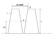
- FIG. 2 shows a glass grid of the present invention
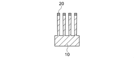
- FIG. 4 shows the lattice of silicon after the Bosch process.
- FIG. 3C is a view corresponding to FIG. 3A and showing a grid with an inversely tapered ridge on the silicon substrate 10;
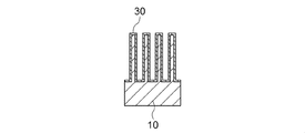
- FIG. 3 shows a grid of silicon after heating;
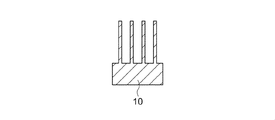
- FIG. 4 shows a lattice of silicon after hydrofluoric acid treatment;
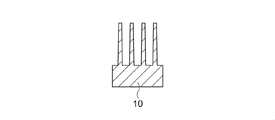
- FIG. 5B is a view corresponding to FIG. 5A and showing a grid with tapered ridges on the silicon substrate 10 after hydrofluoric acid treatment.
- FIG. 11 shows a silicon substrate and a glass plate after anodic bonding;
- FIG. 3C is a view corresponding to FIG. 3A and showing a grid with an inversely tapered ridge on the silicon substrate 10
- FIG. 3 shows a grid of silicon after heating
- FIG. 4 shows a lattice of silicon after hydrofluoric acid treatment
- FIG. 5B is a view corresponding to FIG. 5A and
- FIG. 3 shows a state in which the space formed by the silicon lattice between the silicon substrate and the glass plate is being filled with glass.
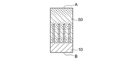
- FIG. 2 is a diagram showing a state in which a space formed by a silicon lattice between a silicon substrate and a glass plate is filled with glass; It is a figure which shows the glass plate after grinding
- the glass plate with grating after step 1070 is shown.
- SEM Sccanning Electron Microscope
- FIG. 1 is an SEM image of a silicon substrate and a glass plate after anodic bonding. 1 is an SEM image of a state in which the space formed by the silicon lattice between the silicon substrate and the glass plate is filled with glass.
- FIG. 8 shows the surface of the glass plate in step 1050 (surface A in FIG. 8) without hydrofluoric acid treatment.
- FIG. 9 is a diagram showing the surface of the glass plate in step 1050 (surface A in FIG.
- 1070 is a cross-sectional SEM image of a glass plate with a grating after step 1070; 1 is a cross-sectional SEM image of a diffraction grating fabricated by a conventional method of plasma etching fused silica; It is a figure which shows the electric furnace used for the heating of a silicon substrate (silicon wafer).
- Fig. 2 shows a chamber in which anodic bonding is performed;
- Fig. 2 shows a chamber in which anodic bonding is performed;
- Fig. 2 shows a chamber in which anodic bonding is performed;
- Fig. 2 shows a chamber in which anodic bonding is performed;
- FIG. 9 is a diagram for explaining polishing of surfaces (surfaces A and B in FIG. 8) opposite to the bonded surfaces of each of the glass plate and the silicon substrate;
- FIG. 2 shows an apparatus for removing silicon in a glass plate by etching with xenon difluoride gas (XeF 2 ). It is a figure for demonstrating how to define a duty ratio when angle (theta) is an acute angle.
- FIG. 1 is a diagram showing the glass lattice of the present invention.
- the glass diffraction grating of the present invention has a grating period P of 0.2 micrometers to 10 micrometers, a grating height h of 0.4 micrometers to 200 micrometers, and a groove aspect ratio h/w of 2 or more.
- w denotes the spacing between ridges r of the grid.
- the duty ratio (P-w)/P is 0.1-0.9.
- the material of the grid is borosilicate glass or barium borosilicate glass.
- FIG. 2 is a flow chart for explaining the method for manufacturing the glass lattice of the present invention.
- a photoresist is applied on the surface of a silicon substrate (silicon wafer) 10, and a grating pattern is formed on the photoresist by a mask exposure device, a laser lithography device, an electron beam lithography device, a stepper, laser interference exposure, or the like.
- the silicon is etched by the Bosch process to form a grating on the surface of the silicon substrate 10 .
- FIG. 3A is a diagram showing the lattice of silicon 10 after the Bosch process. Photoresist 20 remains on the ridges of the silicon grid.
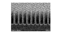
- FIG. 11 is an SEM (Scanning Electron Microscope) image of a silicon substrate 10 with a grid after the Bosch process.
- the image in FIG. 11 corresponds to FIG. 3A.
- the scale depicted in the image of FIG. 11 and other images is graduated in 0.5 micrometer increments.
- the grating period is therefore about 2 micrometers.
- step 1020 of FIG. 2 after removing the resist, the silicon substrate 10 with the grid is heated in a heating furnace to form an oxide film on the surface of the grid.
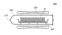
- FIG. 20 shows an electric furnace 200 used for heating the silicon substrate (silicon wafer) 10.
- FIG. A silicon substrate 10 indicated by W is placed in a boat 240 in a quartz tube 220 and heated by a heater 230 from the outside.
- the heating temperature is 1000 degrees (° C.) and the heating time is 20 minutes.
- Oxygen and hydrogen are introduced from the gas inlet 210 into the quartz tube 220, and H 2 O (water vapor) generated by combustion forms an oxide film on the surface of the silicon lattice.
- the thickness of the oxide film is 350 nanometers as an example.
- FIG. 4 is a diagram showing the lattice of silicon 10 after heating.
- An oxide film 30 is formed on the surface of the grating.
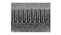
- FIG. 12 is an SEM image of the lattice of silicon 10 after heating. The image in FIG. 12 corresponds to FIG.
- the oxide film on the surface of the grating is removed with hydrofluoric acid. Specifically, the oxide film is removed by immersing the silicon substrate 10 in hydrofluoric acid in a container in a draft chamber.
- FIG. 5A is a diagram showing the lattice of the silicon substrate 10 after hydrofluoric acid treatment.
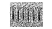
- FIGS. 13 and 14 are SEM images of the lattice of silicon 10 after hydrofluoric acid treatment.
- the image in FIG. 13 is a side view of the grid, and the image in FIG. 14 is a diagonal top view of the grid.
- the images in FIGS. 13 and 14 correspond to FIG. 5A.
- the purpose of removing after forming an oxide film on the surface of the grid by steps 1020 and 1030 of FIG. 2 is to reduce the roughness of the side surfaces of the ridges of the grid.
- a plurality of small scallops are generated in the direction perpendicular to the height direction on the side surface of the ridge of the lattice of the silicon substrate 10 after the Bosch process shown in FIG.
- the height of small undulations is several nanometers to several tens of nanometers.
- step 1020 the ratio of the thickness of the oxide formed on the outside to the thickness of the oxide formed on the inside is about 3:2, based on the original silicon surface. Since the oxide is removed in step 1030 , the above ratios are taken into account to determine the silicon lattice dimensions in step 1010 and the oxide thickness in step 1020 .
- step 1040 of FIG. 2 the gridded surface of the silicon substrate 10 and one surface of the glass plate are anodically bonded in vacuum.
- 21-23 are diagrams showing a chamber 300 in which anodic bonding is performed.
- a silicon substrate 10 with a grid and a glass plate 50 are placed on a base 330 in a chamber 300 such that the surface of the silicon substrate 10 with the grid faces the surface of the glass plate 50, and a rod-shaped substrate is placed between the substrate 10 and the glass plate 50.
- a rod-shaped substrate is placed between the substrate 10 and the glass plate 50.
- FIG. is installed through the spacer 320 of the .
- the chamber 300 is heated to 400° C. with a degree of vacuum of 0.01 to 0.1 Pascal. Due to the presence of the spacers, the spaces between the ridges of the silicon lattice are also at the above-mentioned degree of vacuum.
- the spacer 320 is pulled out to bring the surface of the silicon substrate 10 provided with the lattice and the surface of the glass plate 50 into contact.
- the pressure plate 310 and the base 330 apply a voltage of -500 to -1000 volts to the glass plate. to apply a negative voltage of
- FIG. 24 is a diagram for explaining the principle of anodic bonding.
- Heating the glass plate 50 facilitates the movement of sodium ions (Na + ) in the borosilicate glass or barium borosilicate glass.
- the silicon substrate 10 and the glass plate 50 are connected to the positive and negative electrodes of a voltage source, respectively, and the sodium ions migrate to the negative electrode side.
- a sodium ion-deficient layer is formed near the boundary between the glass plate 50 and the silicon substrate 10 . This layer becomes negatively charged due to the excess of anions.
- a positive charge corresponding to the negative charge is generated, and the surfaces of the two are attracted to each other by the Coulomb force acting between the positive and negative charges and strongly adhere to each other.
- FIG. 6 is a diagram showing the silicon substrate 10 and the glass plate 50 after anodic bonding.
- the vacuum of the space formed by the silicon lattice between the silicon substrate 10 and the glass plate 50 is 0.01-0.1 Pascal as described above.
- FIG. 15 is an SEM image of the silicon substrate 10 and the glass plate 50 after anodic bonding.
- the image in FIG. 15 corresponds to FIG.
- the bonded silicon substrate 10 and glass plate 50 are heated in an electric furnace.
- the electric furnace may be the one shown in FIG.
- the heating temperature is 1100 degrees (°C)
- the heating time is 30 minutes
- the supplied gas is nitrogen.
- the pressure inside the furnace is atmospheric pressure. The heating causes the glass to melt and the atmospheric pressure to fill the low pressure space formed by the silicon lattice between the silicon substrate 10 and the glass plate 50 .
- a hot isostatic pressing device or a hot press device may be used instead of an electric furnace.
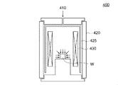
- FIG. 25A is a diagram showing the hot isostatic pressing device 400.
- FIG. The bonded silicon substrate 10 and the glass plate 50 indicated by W are placed in a pressure vessel 420, an inert gas such as argon or nitrogen is introduced into the pressure vessel 420 from the gas inlet 410, and the inside of the pressure vessel 420 is Heating by the heater 430 while applying a pressure of 0.1 to 200 megapascals promotes filling of the space formed by the silicon lattice between the silicon substrate 10 and the glass plate 50 with the glass.
- 425 indicates a heat insulating layer.
- FIG. 25B is a diagram showing a hot press device 400'.
- the bonded silicon substrate 10 and glass plate 50, indicated by W, are placed in a heating chamber 425' within the chamber 420', and an inert gas such as argon or nitrogen is introduced into the chamber 420' through the gas inlet 410'. Then, the space formed by the silicon lattice between the silicon substrate 10 and the glass plate 50 is filled with glass by heating with the heater 430 ′ while applying pressure to the workpiece with the cylinder 405 ′.
- an inert gas such as argon or nitrogen
- FIG. 7 shows a state in which the space formed by the silicon lattice between the silicon substrate 10 and the glass plate 50 is being filled with glass.
- FIG. 8 is a diagram showing a state in which the space formed by the silicon lattice between the silicon substrate 10 and the glass plate 50 is filled with glass.
- the glass filled between the ridges of the silicon grid forms a glass grid.
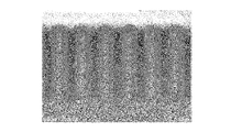
- FIG. 16 is an SEM image of a state in which the space formed by the silicon lattice between the silicon substrate 10 and the glass plate 50 is filled with glass.
- the image in FIG. 16 corresponds to FIG.
- step 1040 or step 1050 When the borosilicate glass or barium borosilicate glass is heated in steps 1040 and 1050, additives such as sodium and aluminum contained in the glass may precipitate on the surface of the glass plate 50 and deteriorate the optical characteristics of the diffraction grating. . Therefore, before step 1040 or step 1050, it is desirable to etch the surface of the glass plate 50 with hydrofluoric acid by about 500 nanometers to remove the additives near the surface.
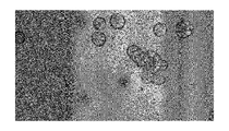
- FIG. 17 is a diagram showing the surface of the glass plate 50 (surface A in FIG. 8) in step 1050 without hydrofluoric acid treatment.
- FIG. 18 is a diagram showing the surface of the glass plate 50 (surface A in FIG. 8) in step 1050 when hydrofluoric acid treatment is performed.
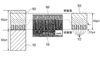
- step 1060 in FIG. 2 the surfaces of the glass plate 50 and the silicon substrate 10 opposite to the bonded surfaces (surfaces A and B in FIG. 8) are polished.
- FIG. 26 is a diagram for explaining the polishing of the surfaces of the glass plate 50 and the silicon substrate 10 opposite to the bonded surfaces (surfaces A and B in FIG. 8).
- the silicon substrate is removed by polishing except for the lattice portion surrounded by glass. Polishing is performed by a CMP (Chemical Mechanical Polishing) method.
- the roughness of each surface after polishing is less than 1 nanometer.
- the thickness of the glass plate 50 and silicon substrate 10 before polishing is 500 micrometers respectively.
- the thickness of the glass plate after polishing is 400 micrometers, and the height (depth) of the grating is 6.5 micrometers.
- FIG. 9 is a diagram showing the glass plate 50 after polishing. Silicon 10' remains between the ridges of the glass grid.
- step 1070 of FIG. 2 the silicon between the ridges of the glass grid is removed by selective etching with xenon difluoride gas (XeF2).
- XeF2 xenon difluoride gas
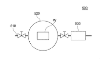
- FIG. 27 shows an apparatus 500 for removing silicon from the glass plate 50 by etching with xenon difluoride gas (XeF 2 ).
- a glass plate 50 indicated by W is placed in a vacuum chamber 520 , and a xenon difluoride gas (XeF 2 ) is introduced into the vacuum chamber 520 from a gas inlet 510 by a rotary pump 530 .
- Xenon (Xe) and fluorine (F) have a weak bond, so silicon (Si) reacts with fluorine (F) to form silicon tetrafluoride (SiF 4 ), which evaporates. Etching of (Si) proceeds selectively.
- silicon oxide such as silicon monoxide (SiO) remains unetched, a thermal oxidation process is added to convert it to silicon dioxide (SiO 2 ), which changes the refractive index to the same level as glass.
- SiO 2 silicon dioxide
- Wet oxidation which has a high oxidation rate, is desirable for thermal oxidation.
- FIG. 10 shows the glass plate 50 with gratings after step 1070 .
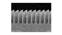
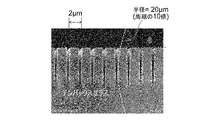
- FIG. 19A is a cross-sectional SEM image of the glass plate 50 with the grating after step 1070.
- FIG. The image in FIG. 19A corresponds to FIG.
- the grating period is 2 micrometers
- the grating depth (height) is 6 micrometers
- the groove aspect ratio is 14, and the duty ratio is 0.785.
- the side of the rectangular ridge in the direction of the period and the direction of almost the height The angle (acute angle) ⁇ formed by the sides of is 88 degrees.
- FIG. 28 is a diagram for explaining how to determine the duty ratio when the angle ⁇ is an acute angle.
- the spacing w between the ridges r of the grid is determined at a height half the height h of the ridges.
- the above angle (acute angle) ⁇ is preferably in the range of 70 degrees or more and less than 90 degrees. The reason is as follows.
- the oxide film 30 shown in FIG. 4 actually becomes thicker as it approaches the upper surface of the grating. Therefore, when the oxide film 30 is removed in step S1030, the cross-sectional shape of the ridges of the grid becomes a tapered shape in which the width becomes narrower toward the upper surface of the grid.
- FIG. 5B is a view corresponding to FIG. 5A and showing a grid with tapered ridges of the silicon substrate 10 after hydrofluoric acid treatment.
- the cross-sectional shape of the ridges of the glass lattice also becomes a tapered shape with a narrower width closer to the upper surface of the lattice. That is, the angle ⁇ formed by the side in the direction of the period of the rectangular cross section and the side in the direction of the height is an acute angle.
- the cross-sectional shape of the ridges of the grid can be formed into an inverse tapered shape in which the width is wider toward the upper surface of the grid.
- FIG. 3B is a view corresponding to FIG. 3A and showing a grating with ridges of the silicon substrate 10 having an inverse tapered shape.
- the angle ( ⁇ in FIG. 19A) formed by the sides in the periodic direction and the sides in the approximate height direction of the rectangular ridges can be adjusted.
- the radius of curvature of the sides in the substantially height direction of the rectangular cross section formed by the direction of the period of the diffraction grating and the direction of the height is greater than 10 times the period of the diffraction grating.
- FIG. 19B is a cross-sectional SEM image of a diffraction grating manufactured by a conventional method of plasma etching quartz glass.
- the radius of curvature of the sides in the height direction of the rectangular cross section formed by the direction of the period of the diffraction grating and the direction of the height of the diffraction grating is about three times the period of the diffraction grating.
- the large radius of curvature makes it possible to obtain significantly improved optical characteristics of the diffraction grating compared to the prior art.
Landscapes
- Physics & Mathematics (AREA)
- General Physics & Mathematics (AREA)
- Optics & Photonics (AREA)
- Engineering & Computer Science (AREA)
- Manufacturing & Machinery (AREA)
- Diffracting Gratings Or Hologram Optical Elements (AREA)
Abstract
Description
Claims (7)
- 周期が0.2~10マイクロメータ、溝のアスペクト比が2以上のホウケイ酸ガラスまたはバリウムホウケイ酸ガラスの回折格子の製造方法であって、
ケイ素基板の表面にボッシュプロセスにより格子を形成するステップと、
1,000℃前後に加熱し、水蒸気を暴露することによって該格子の表面に酸化膜を形成するステップと、
フッ化水素酸により該酸化膜を除去するステップと、
該ケイ素基板の該格子を備えた面とガラス板の一つの面とを0.01~0.1パスカルの容器内で陽極接合するステップと、
ガラスを溶融させケイ素からなる該格子の畝部の間に充填させるように、接合された該ケイ素基板及び該ガラス板を加熱するステップと、
該ケイ素基板及び該ガラス板のそれぞれの、接合された面と反対側の面を研磨するステップと、
該ガラス板からケイ素を二フッ化キセノンガスによる選択的エッチングにより除去するステップと、を含むガラス回折格子の製造方法。 - 該ガラス板からケイ素を選択的エッチングにより除去するステップの後に、該ガラス板を1,000℃前後に加熱し、水蒸気を暴露するステップを含む請求項1に記載のガラス回折格子の製造方法。
- 周期が0.2~10マイクロメータ、溝のアスペクト比が2以上のホウケイ酸ガラスまたはバリウムホウケイ酸ガラスの回折格子。
- 該回折格子の周期の方向及び高さの方向を含む断面において、矩形状の畝部の側面に対応する辺の曲率半径は、回折格子の周期の10倍よりも大きい請求項3に記載のガラス回折格子。
- 該格子の周期に対する該格子の畝部の幅が0.1から0.9の範囲である請求項3または4に記載のガラス回折格子。
- 該格子の畝部の側面の粗さが10ナノメータ以下である請求項3から5のいずれかに記載のガラス回折格子。
- 該回折格子の周期の方向及び高さの方向によって形成される断面において矩形状の格子の畝部の周期の方向の辺およびほぼ高さの方向の辺のなす角度が70度以上かつ90度未満の範囲である請求項3から6のいずれかに記載のガラス回折格子。
Priority Applications (3)
| Application Number | Priority Date | Filing Date | Title |
|---|---|---|---|
| JP2022541660A JP7171007B1 (ja) | 2021-03-24 | 2022-02-21 | ガラス回折格子及びその製造方法 |
| CN202280021095.8A CN116981967A (zh) | 2021-03-24 | 2022-02-21 | 玻璃衍射光栅及其制造方法 |
| US18/468,120 US12613364B2 (en) | 2021-03-24 | 2023-09-15 | Glass diffraction grating and method of producing the same |
Applications Claiming Priority (2)
| Application Number | Priority Date | Filing Date | Title |
|---|---|---|---|
| US202163165361P | 2021-03-24 | 2021-03-24 | |
| US63/165,361 | 2021-03-24 |
Related Child Applications (1)
| Application Number | Title | Priority Date | Filing Date |
|---|---|---|---|
| US18/468,120 Continuation US12613364B2 (en) | 2021-03-24 | 2023-09-15 | Glass diffraction grating and method of producing the same |
Publications (1)
| Publication Number | Publication Date |
|---|---|
| WO2022202033A1 true WO2022202033A1 (ja) | 2022-09-29 |
Family
ID=83397036
Family Applications (1)
| Application Number | Title | Priority Date | Filing Date |
|---|---|---|---|
| PCT/JP2022/006859 Ceased WO2022202033A1 (ja) | 2021-03-24 | 2022-02-21 | ガラス回折格子及びその製造方法 |
Country Status (4)
| Country | Link |
|---|---|
| US (1) | US12613364B2 (ja) |
| JP (1) | JP7171007B1 (ja) |
| CN (1) | CN116981967A (ja) |
| WO (1) | WO2022202033A1 (ja) |
Families Citing this family (1)
| Publication number | Priority date | Publication date | Assignee | Title |
|---|---|---|---|---|
| US20250076550A1 (en) * | 2023-08-28 | 2025-03-06 | Modulight Corporation | System and method for fabricating high-aspect-ratio gratings |
Citations (9)
| Publication number | Priority date | Publication date | Assignee | Title |
|---|---|---|---|---|
| JP2002048907A (ja) * | 2000-08-01 | 2002-02-15 | Canon Inc | 回折光学素子の製作方法 |
| JP2004093634A (ja) * | 2002-08-29 | 2004-03-25 | Nippon Sheet Glass Co Ltd | 構造体の形成方法 |
| JP2005037872A (ja) * | 2003-01-28 | 2005-02-10 | Nippon Sheet Glass Co Ltd | 光学素子およびそれを備えた光回路並びに光分波器 |
| US20120198935A1 (en) * | 2009-10-06 | 2012-08-09 | Scott Samson | Twin sub-wavelength grating optical signal processor |
| WO2018100868A1 (ja) * | 2016-12-02 | 2018-06-07 | 日本碍子株式会社 | 光学素子及びその製造方法 |
| WO2018155556A1 (ja) * | 2017-02-23 | 2018-08-30 | デンカ株式会社 | フォトニック結晶 |
| JP2019510998A (ja) * | 2016-01-30 | 2019-04-18 | レイア、インコーポレイテッドLeia Inc. | プライバシーディスプレイおよびデュアルモードプライバシーディスプレイシステム |
| JP2020056973A (ja) * | 2018-10-04 | 2020-04-09 | 国立研究開発法人理化学研究所 | 石英製の格子構造体および回折格子ならびに製造方法 |
| US20200249377A1 (en) * | 2019-01-31 | 2020-08-06 | Canon U.S.A., Inc. | Diffractive optical device, endoscopic probe, and fabrication methods therefor |
Family Cites Families (8)
| Publication number | Priority date | Publication date | Assignee | Title |
|---|---|---|---|---|
| US20030092075A1 (en) * | 2000-10-30 | 2003-05-15 | Sru Biosystems, Llc | Aldehyde chemical surface activation processes and test methods for colorimetric resonant sensors |
| US7349612B2 (en) | 2003-01-28 | 2008-03-25 | Nippon Sheet Glass Company, Limited | Optical element, optical circuit provided with the optical element, and method for producing the optical element |
| DE102004020363A1 (de) * | 2004-04-23 | 2005-11-17 | Schott Ag | Verfahren zur Herstellung eines Masters, Master und Verfahren zur Herstellung von optischen Elementen sowie optischen Element |
| CA2824148C (en) * | 2011-01-14 | 2016-01-05 | Jx Nippon Oil & Energy Corporation | Method for producing mold for minute pattern transfer, method for producing diffraction grating using the same, and method for producing organic el element including the diffraction grating |
| FR2981460B1 (fr) * | 2011-10-18 | 2016-06-24 | Commissariat Energie Atomique | Procede de realisation d'un dispositif optique refractif ou diffractif |
| JP6058402B2 (ja) * | 2012-06-08 | 2017-01-11 | 株式会社日立ハイテクノロジーズ | 曲面回折格子の製造方法、および曲面回折格子の型 |
| US9970119B2 (en) * | 2013-10-25 | 2018-05-15 | Konica Minolta, Inc. | Curved grating structure manufacturing method, curved grating structure, grating unit, and x-ray imaging device |
| JP6779984B2 (ja) | 2015-09-05 | 2020-11-04 | レイア、インコーポレイテッドLeia Inc. | 集光型バックライトおよびそれを使用するニアアイディスプレイシステム |
-
2022
- 2022-02-21 WO PCT/JP2022/006859 patent/WO2022202033A1/ja not_active Ceased
- 2022-02-21 CN CN202280021095.8A patent/CN116981967A/zh active Pending
- 2022-02-21 JP JP2022541660A patent/JP7171007B1/ja active Active
-
2023
- 2023-09-15 US US18/468,120 patent/US12613364B2/en active Active
Patent Citations (9)
| Publication number | Priority date | Publication date | Assignee | Title |
|---|---|---|---|---|
| JP2002048907A (ja) * | 2000-08-01 | 2002-02-15 | Canon Inc | 回折光学素子の製作方法 |
| JP2004093634A (ja) * | 2002-08-29 | 2004-03-25 | Nippon Sheet Glass Co Ltd | 構造体の形成方法 |
| JP2005037872A (ja) * | 2003-01-28 | 2005-02-10 | Nippon Sheet Glass Co Ltd | 光学素子およびそれを備えた光回路並びに光分波器 |
| US20120198935A1 (en) * | 2009-10-06 | 2012-08-09 | Scott Samson | Twin sub-wavelength grating optical signal processor |
| JP2019510998A (ja) * | 2016-01-30 | 2019-04-18 | レイア、インコーポレイテッドLeia Inc. | プライバシーディスプレイおよびデュアルモードプライバシーディスプレイシステム |
| WO2018100868A1 (ja) * | 2016-12-02 | 2018-06-07 | 日本碍子株式会社 | 光学素子及びその製造方法 |
| WO2018155556A1 (ja) * | 2017-02-23 | 2018-08-30 | デンカ株式会社 | フォトニック結晶 |
| JP2020056973A (ja) * | 2018-10-04 | 2020-04-09 | 国立研究開発法人理化学研究所 | 石英製の格子構造体および回折格子ならびに製造方法 |
| US20200249377A1 (en) * | 2019-01-31 | 2020-08-06 | Canon U.S.A., Inc. | Diffractive optical device, endoscopic probe, and fabrication methods therefor |
Also Published As
| Publication number | Publication date |
|---|---|
| JPWO2022202033A1 (ja) | 2022-09-29 |
| US20240004111A1 (en) | 2024-01-04 |
| US12613364B2 (en) | 2026-04-28 |
| JP7171007B1 (ja) | 2022-11-15 |
| CN116981967A (zh) | 2023-10-31 |
Similar Documents
| Publication | Publication Date | Title |
|---|---|---|
| US6358854B1 (en) | Method to fabricate layered material compositions | |
| US9529127B2 (en) | Method for producing a refractive or diffractive optical device | |
| US20140272688A1 (en) | Grayscale lithography of photo definable glass | |
| US20080257860A1 (en) | Method for microstructuring flat glass substrates | |
| JP5264237B2 (ja) | ナノ構造体およびナノ構造体の製造方法 | |
| CN113168020A (zh) | 用于形成光栅的方法 | |
| JP7171007B1 (ja) | ガラス回折格子及びその製造方法 | |
| CN115494567B (zh) | 一种微透镜阵列纳米光栅的复合结构及制备方法、应用 | |
| JP4940784B2 (ja) | インプリント用モールドおよびインプリント用モールド製造方法 | |
| JP2009027176A (ja) | 微小電気機械システムに使用するためのウェーハを製造する方法 | |
| US20030064585A1 (en) | Manufacture of semiconductor device with spacing narrower than lithography limit | |
| JP3833274B2 (ja) | X線マスクの製造方法 | |
| CN115494568B (zh) | 一种微透镜阵列的制备方法及其微透镜阵列、应用 | |
| US6627468B2 (en) | Method for manufacturing optical element, optical element, optical system using optical element, optical apparatus and exposure apparatus using optical system, and method for manufacturing device | |
| JP4681644B2 (ja) | 光導波路の作製方法 | |
| JP4983313B2 (ja) | 転写マスクおよびその製造方法 | |
| JP2010183208A (ja) | ウエットエッチング方法及び音叉型圧電素子片の加工方法 | |
| JP5332776B2 (ja) | 転写マスクの製造方法 | |
| JP2004014652A (ja) | 微細パターンの形成方法 | |
| JP5326192B2 (ja) | インプリント用モールド及びインプリント用モールド製造方法 | |
| JP5003321B2 (ja) | マスクブランクおよびマスクブランク製造方法 | |
| JP2006245462A (ja) | 転写マスクの製造方法 | |
| US20060249863A1 (en) | Prism manufacturing method | |
| WO2024218966A1 (ja) | レリーフ型回折格子の製造方法 | |
| JP3944585B2 (ja) | ドライエッチングによる垂直面作製方法 |
Legal Events
| Date | Code | Title | Description |
|---|---|---|---|
| ENP | Entry into the national phase |
Ref document number: 2022541660 Country of ref document: JP Kind code of ref document: A |
|
| 121 | Ep: the epo has been informed by wipo that ep was designated in this application |
Ref document number: 22774833 Country of ref document: EP Kind code of ref document: A1 |
|
| WWE | Wipo information: entry into national phase |
Ref document number: 202280021095.8 Country of ref document: CN |
|
| NENP | Non-entry into the national phase |
Ref country code: DE |
|
| 122 | Ep: pct application non-entry in european phase |
Ref document number: 22774833 Country of ref document: EP Kind code of ref document: A1 |