WO2022202006A1 - 光電変換素子及びその製造方法並びに撮像装置 - Google Patents
光電変換素子及びその製造方法並びに撮像装置 Download PDFInfo
- Publication number
- WO2022202006A1 WO2022202006A1 PCT/JP2022/006473 JP2022006473W WO2022202006A1 WO 2022202006 A1 WO2022202006 A1 WO 2022202006A1 JP 2022006473 W JP2022006473 W JP 2022006473W WO 2022202006 A1 WO2022202006 A1 WO 2022202006A1
- Authority
- WO
- WIPO (PCT)
- Prior art keywords
- photoelectric conversion
- compound semiconductor
- conductivity
- type region
- semiconductor layer
- Prior art date
- Legal status (The legal status is an assumption and is not a legal conclusion. Google has not performed a legal analysis and makes no representation as to the accuracy of the status listed.)
- Ceased
Links
Images









Classifications
-
- H—ELECTRICITY
- H10—SEMICONDUCTOR DEVICES; ELECTRIC SOLID-STATE DEVICES NOT OTHERWISE PROVIDED FOR
- H10F—INORGANIC SEMICONDUCTOR DEVICES SENSITIVE TO INFRARED RADIATION, LIGHT, ELECTROMAGNETIC RADIATION OF SHORTER WAVELENGTH OR CORPUSCULAR RADIATION
- H10F30/00—Individual radiation-sensitive semiconductor devices in which radiation controls the flow of current through the devices, e.g. photodetectors
- H10F30/20—Individual radiation-sensitive semiconductor devices in which radiation controls the flow of current through the devices, e.g. photodetectors the devices having potential barriers, e.g. phototransistors
-
- H—ELECTRICITY
- H10—SEMICONDUCTOR DEVICES; ELECTRIC SOLID-STATE DEVICES NOT OTHERWISE PROVIDED FOR
- H10F—INORGANIC SEMICONDUCTOR DEVICES SENSITIVE TO INFRARED RADIATION, LIGHT, ELECTROMAGNETIC RADIATION OF SHORTER WAVELENGTH OR CORPUSCULAR RADIATION
- H10F39/00—Integrated devices, or assemblies of multiple devices, comprising at least one element covered by group H10F30/00, e.g. radiation detectors comprising photodiode arrays
- H10F39/10—Integrated devices
- H10F39/12—Image sensors
-
- H—ELECTRICITY
- H10—SEMICONDUCTOR DEVICES; ELECTRIC SOLID-STATE DEVICES NOT OTHERWISE PROVIDED FOR
- H10F—INORGANIC SEMICONDUCTOR DEVICES SENSITIVE TO INFRARED RADIATION, LIGHT, ELECTROMAGNETIC RADIATION OF SHORTER WAVELENGTH OR CORPUSCULAR RADIATION
- H10F39/00—Integrated devices, or assemblies of multiple devices, comprising at least one element covered by group H10F30/00, e.g. radiation detectors comprising photodiode arrays
- H10F39/80—Constructional details of image sensors
- H10F39/802—Geometry or disposition of elements in pixels, e.g. address-lines or gate electrodes
- H10F39/8023—Disposition of the elements in pixels, e.g. smaller elements in the centre of the imager compared to larger elements at the periphery
-
- H—ELECTRICITY
- H10—SEMICONDUCTOR DEVICES; ELECTRIC SOLID-STATE DEVICES NOT OTHERWISE PROVIDED FOR
- H10F—INORGANIC SEMICONDUCTOR DEVICES SENSITIVE TO INFRARED RADIATION, LIGHT, ELECTROMAGNETIC RADIATION OF SHORTER WAVELENGTH OR CORPUSCULAR RADIATION
- H10F71/00—Manufacture or treatment of devices covered by this subclass
- H10F71/127—The active layers comprising only Group III-V materials, e.g. GaAs or InP
- H10F71/1272—The active layers comprising only Group III-V materials, e.g. GaAs or InP comprising at least three elements, e.g. GaAlAs or InGaAsP
-
- H—ELECTRICITY
- H10—SEMICONDUCTOR DEVICES; ELECTRIC SOLID-STATE DEVICES NOT OTHERWISE PROVIDED FOR
- H10F—INORGANIC SEMICONDUCTOR DEVICES SENSITIVE TO INFRARED RADIATION, LIGHT, ELECTROMAGNETIC RADIATION OF SHORTER WAVELENGTH OR CORPUSCULAR RADIATION
- H10F77/00—Constructional details of devices covered by this subclass
- H10F77/10—Semiconductor bodies
- H10F77/12—Active materials
- H10F77/124—Active materials comprising only Group III-V materials, e.g. GaAs
- H10F77/1248—Active materials comprising only Group III-V materials, e.g. GaAs having three or more elements, e.g. GaAlAs, InGaAs or InGaAsP
Definitions
- the present disclosure relates to a photoelectric conversion element, its manufacturing method, and an imaging device.
- NIR near infrared
- SWIR shortwave infrared
- the present disclosure provides a photoelectric conversion element capable of further suppressing color mixture, a manufacturing method thereof, and an imaging apparatus.
- a first compound semiconductor layer made of a first compound semiconductor material having a first conductivity type; a photoelectric conversion layer formed in contact with the first compound semiconductor layer; a second compound semiconductor layer formed in contact with the photoelectric conversion layer and made of a second compound semiconductor material having the first conductivity type; a first second conductivity type region formed in at least part of the second compound semiconductor layer, having a second conductivity type different from the first conductivity type, and reaching the photoelectric conversion layer; a second second-conductivity-type region formed in at least a portion of the second compound semiconductor layer, having the second conductivity type, and reaching the photoelectric conversion layer, the first second-conductivity-type region being formed in at least a portion of the second compound semiconductor layer; a second second conductivity type region having a region different from A photoelectric conversion device is provided.
- a first electrode electrically connected to the first compound semiconductor layer; a second electrode formed on the second conductivity type region; may be further provided.
- the first second-conductivity-type region and the second second-conductivity-type region may have different impurity concentrations.
- the first second-conductivity-type region has a lower impurity concentration than the second second-conductivity-type region, and the first second-conductivity-type region is higher than the second second-conductivity-type region. It may be formed closer to the first compound semiconductor layer.
- a third second-conductivity-type region formed in at least a portion of the second compound semiconductor layer, having the second conductivity type, and reaching the photoelectric conversion layer, the first second-conductivity-type region being formed in at least a portion of the second compound semiconductor layer; , and a third second conductivity type region having a region different from the second second conductivity type region.
- the first second-conductivity-type region and the second second-conductivity-type region may be formed by diffusing impurities under different conditions.
- the first second-conductivity-type region and the second second-conductivity-type region may be formed by diffusing the impurity from different positions.
- the first second-conductivity-type region has a higher impurity concentration than the second second-conductivity-type region, and is formed closer to the first compound semiconductor layer than the second second-conductivity-type region.
- the second second conductivity type region may have two convex regions along the second compound semiconductor layer.
- a plurality of layers having different impurity concentrations may be stacked in the photoelectric conversion layer.
- the first electrode may be formed on the light incident side surface of the first compound semiconductor layer.
- the first compound semiconductor layer and the second compound semiconductor layer may be made of the same material.
- the first compound semiconductor layer and the second compound semiconductor layer may be made of a III-V group compound semiconductor material.
- the photoelectric conversion layer is made of InGaAs
- the first compound semiconductor layer and the second compound semiconductor layer may be made of InP.
- Light may enter through the first compound semiconductor layer.
- a plurality of photoelectric conversion elements may be arranged in a two-dimensional matrix.
- a first compound semiconductor layer made of a first compound semiconductor material having a first conductivity type, a photoelectric conversion layer, and a second compound semiconductor layer made of a second compound semiconductor material having a first conductivity type are sequentially formed, forming a first second conductivity type region having a second conductivity type different from the first conductivity type and reaching the photoelectric conversion layer in at least part of the second compound semiconductor layer;
- a second second conductivity type region having the second conductivity type and reaching the photoelectric conversion layer is formed in at least a part of the second compound semiconductor layer under conditions different from those of the first second conductivity type region.
- a method for manufacturing a photoelectric conversion element including steps.
- An impurity may be diffused from the second compound semiconductor layer through a mask layer to form the first second conductivity type region and the second second conductivity type region.
- an impurity is diffused from the second compound semiconductor layer through a first mask layer, the impurity is diffused through a second mask layer after removing the first mask layer, and the second second conductivity type region is formed; may be formed.
- At least one of impurity concentration, temperature, and time may be different between the state of diffusing impurities through the first mask layer and the state of diffusing impurities through the second mask layer.
- FIG. 1 is a diagram showing a configuration example of an imaging device according to a first embodiment
- FIG. 1 is a schematic partial cross-sectional view of a photoelectric conversion element according to this embodiment
- FIG. 4 is a diagram showing the relationship between the position and concentration of a first second-conductivity-type region and a second second-conductivity-type region
- FIG. 2 is a schematic partial cross-sectional view of a photoelectric conversion element according to a comparative example
- FIG. 4 is a schematic diagram showing a step of forming a first second-conductivity-type region and a second second-conductivity-type region
- FIG. 4A is a plan view of a mask layer used in forming the first second-conductivity-type region
- FIG. 4A is a plan view of a mask layer used in forming the first second-conductivity-type region
- FIG. 4 is a plan view of a mask layer used in creating a second second conductivity type region; Schematic diagram showing a step of generating a first electrode and a second electrode.
- FIG. 2 is a schematic partial cross-sectional view of a photoelectric conversion element according to a second embodiment;
- FIG. 4 is a diagram showing the relationship between the position and concentration of first to third second-conductivity-type regions;
- FIG. 4 is a schematic diagram showing steps of forming first to third second-conductivity-type regions;
- FIG. 11 is a plan view of a mask layer used in creating a third second-conductivity-type region; The typical partial cross section figure of the photoelectric conversion element concerning a 3rd embodiment.
- FIG. 11 is a plan view of a mask layer used in forming the fifth second conductivity type region;
- FIG. 11 is a schematic diagram showing a step of forming fourth and fifth second-conductivity-type regions;
- FIG. 4 is a diagram showing the relationship between the position and concentration of a photoelectric conversion layer and a second second-conductivity-type region;
- FIG. 11 is a diagram for explaining an example of a method for manufacturing a photoelectric conversion element according to the fourth embodiment;
- FIG. 11 is a schematic partial cross-sectional view of a photoelectric conversion element 101 according to a fifth embodiment
- FIG. 4 is a diagram showing the relationship between the position and concentration of a photoelectric conversion layer and first and second second-conductivity-type regions
- FIG. 11 is a diagram for explaining an example of a method for manufacturing a photoelectric conversion element according to the fifth embodiment
- FIG. 2 is a conceptual diagram showing an example in which the disclosed imaging device is used in an electronic device;
- FIG. 1 is a diagram illustrating a configuration example of an imaging device 100 according to the first embodiment of the present technology.
- the image pickup apparatus 100 includes an image pickup area 111 in which photoelectric conversion elements 101 are arranged in a two-dimensional matrix (two-dimensional array), and a vertical drive circuit 112 as a drive circuit (peripheral circuit). , a column signal processing circuit 113, a horizontal drive circuit 114, an output circuit 115, a drive control circuit 116, and the like.
- These circuits can be configured from well-known circuits, or can be configured using other circuit configurations (for example, various circuits used in conventional CCD-type imaging devices and CMOS-type imaging devices). It is possible. That is, the imaging device 100 can generate an electric field in the photoelectric conversion element 101 by means of the Zn diffusion regions in multiple stages, and can suppress color mixture between pixels.
- the drive control circuit 116 generates clock signals and control signals that serve as operational references for the vertical drive circuit 112, the column signal processing circuit 113, and the horizontal drive circuit 114, based on the vertical synchronization signal, horizontal synchronization signal, and master clock.
- the generated clock signal and control signal are input to the vertical drive circuit 112 , the column signal processing circuit 113 and the horizontal drive circuit 114 .
- the vertical drive circuit 112 is composed of, for example, a shift register, and sequentially selectively scans the photoelectric conversion elements 101 in the imaging area 111 in units of rows in the vertical direction.
- a pixel signal (image signal) based on a current (signal) generated according to the amount of light received by each photoelectric conversion element 101 is sent to the column signal processing circuit 113 via a signal line (data output line) 117 .
- the column signal processing circuit 113 is arranged, for example, for each column of the photoelectric conversion elements 101, and converts image signals output from the photoelectric conversion elements 101 for one row into black reference pixels (not shown, effective Signal processing such as noise removal and signal amplification is performed on the basis of signals from (formed around the pixel area).
- a horizontal selection switch (not shown) is provided at the output stage of the column signal processing circuit 113 so as to be connected between it and the horizontal signal line 118 .
- the horizontal driving circuit 114 is composed of, for example, a shift register, and sequentially outputs horizontal scanning pulses to sequentially select each of the column signal processing circuits 113 and transmit signals from each of the column signal processing circuits 113 to the horizontal signal line 118 . Output.
- the output circuit 115 performs signal processing on signals sequentially supplied from each of the column signal processing circuits 113 via the horizontal signal line 118 and outputs the processed signals.
- the imaging device 100 can constitute an electronic device having an imaging function, such as a digital still camera, a video camera, a camcorder, an in-vehicle camera, a surveillance camera, and a mobile phone.
- the configuration and structure of the imaging device excluding the photoelectric conversion element can be the same as the configuration and structure of a well-known imaging device, and various processing of signals obtained by the photoelectric conversion element can be performed based on well-known circuits. can.
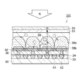
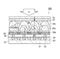
- FIG. 2 is a schematic partial cross-sectional view of the photoelectric conversion element 101 according to this embodiment.
- the photoelectric conversion element 101 includes, for example, a support substrate 23, an insulating film 24, a first compound semiconductor layer 31, a second compound semiconductor layer 32, a reflective film 33, a photoelectric conversion layer 34, a first second conductivity type region 35a, a second second conductivity type region 35 b , covering layer 36 , first electrode 51 and second electrode 52 .
- the second electrode 52 is formed on the same side as the first electrode 51 .
- the first electrode 51 is electrically connected to the first compound semiconductor layer 31 .
- the second electrode 52 is electrically connected to the second conductivity type regions 35a and 35b.
- the imaging device 100 (see FIG. 1) of the present disclosure further includes a driving substrate 60, for example, a readout integrated substrate (ROIC substrate, Read Only IC substrate), and the first electrodes constituting each photoelectric conversion element 101 51 is connected to a first electrode connection portion provided on the drive substrate 60 .
- the second electrode 52 forming each photoelectric conversion element 101 is connected to a second electrode connection portion provided on the drive substrate 60 .
- the first conductivity type is n-type
- the second conductivity type is p-type.
- the first compound semiconductor layer 31 and the second compound semiconductor layer 32 are made of the same material.
- the first compound semiconductor layer 31, the second compound semiconductor layer 32, and the photoelectric conversion layer 34 are made of III-V compound semiconductor materials.
- the photoelectric conversion layer 34 is made of InGaAs (specifically, n-InGaAs, more specifically, n-In0.57Ga0.43As), and the first compound semiconductor layer 31 and the second compound semiconductor layer 32 are It is made of InP (specifically, n+-InP).
- the impurity concentration Im0 of the photoelectric conversion layer 34 is 5 ⁇ 10 16 cm ⁇ 3 or less
- the impurity concentrations Im1 and Im2 of the first compound semiconductor layer 31 and the second compound semiconductor layer 32 are also 5 ⁇ 10 17 cm ⁇ 3 to 5 ⁇ 10 17 cm ⁇ 3 . 5 ⁇ 10 18 cm ⁇ 3 .
- the first conductivity type may be p-type
- the second conductivity type may be n-type.
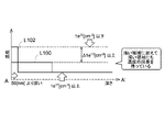
- FIG. 3 is a diagram showing the relationship between the position and concentration of the first second-conductivity-type region 35a and the second second-conductivity-type region 35b.
- the vertical axis indicates the concentration
- the horizontal axis indicates the position on the AA' line (see FIG. 2).
- the position of the lower surface of the second compound semiconductor layer 32 is indicated by 0 as the Zn diffusion surface, and the position from the Zn diffusion surface is indicated as the depth.
- the first second conductivity type region 35a and the second second conductivity type region 35b are generated by Zn diffusion, for example.
- a line L100 indicates the relationship between the depth of the first second conductivity type region 35a and the impurity concentration.
- a line L102 indicates the relationship between the depth of the second second conductivity type region 35b and the impurity concentration.
- a second impurity concentration of, for example, 1e 20 [cm ⁇ 3 ] is formed deeper than 50 nm in the depth direction of the center of the pixel in the second compound semiconductor layer 32 and the photoelectric conversion layer 34 .
- a two-conductivity type region 35b is formed.
- the second second-conductivity-type region 35b may have a concentration range of, for example, 1e 17 [cm ⁇ 3 ] to 1e 20 [cm ⁇ 3 ].
- the first second-conductivity-type region 35a is configured to have, for example, a concentration difference of 1e 17 [cm ⁇ 3 ] with respect to the impurity concentration of the second second-conductivity-type region 35b.
- Zn is diffused thinly and deeply, and in addition, shallow Zn is diffused to form a structure in which a plurality of concentration distributions are combined.
- the first second-conductivity-type region 35a and the second second-conductivity-type region 35b allow more holes, which are carriers, to be collected in the second electrode 52.
- the first electrode 51 and the second electrode 52 according to the present embodiment are provided on the same side, the present invention is not limited to this.
- the first electrode 51 may be provided on the first compound semiconductor layer 31 side.
- FIG. 4 is a schematic partial cross-sectional view of a photoelectric conversion element 101 according to a comparative example.
- a photoelectric conversion element 101 according to a comparative example is an example in which the first second conductivity type region 35a is not formed. Since the first second-conductivity-type region 35a is not formed, holes, which are carriers generated on the incident light side of the photoelectric conversion layer 34, are more likely to move to adjacent pixels.
- the photoelectric conversion element 101 since the first second conductivity type region 35a is further formed, the light generated on the incident light side of the photoelectric conversion layer 34 Holes, which are carriers, can also be collected by the second electrode 52 due to the electric field generated at the boundary of the first second-conductivity-type region 35a, and color mixture can be further suppressed. That is, by forming the two-stage second conductivity type regions 35 a and 35 b , an electric field can be generated to attract more carriers (eg, holes) to the second electrode 52 . As a result, carriers generated in a predetermined range (corresponding to the pixel range) above the second electrode 52 can be collected by the second electrode 52 within the same pixel.
- carriers generated in a predetermined range corresponding to the pixel range
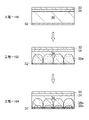
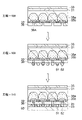
- FIG. 5 is a schematic diagram showing a process of forming the first second-conductivity-type region 35a and the second second-conductivity-type region 35b.
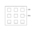
- FIG. 6 shows a plan view of a mask layer 300 used in forming the first second conductivity type region 35a.
- An opening 300 a is formed in the mask layer 300 .
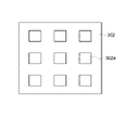
- FIG. 7 shows a plan view of a mask layer 302 used in creating the second second conductivity type region 35b.
- An opening 302 a is formed in the mask layer 302 .
- the area of the opening 300a is formed larger than the area of the opening 302a.
- a semiconductor layer 32 is sequentially formed. Specifically, a deposition substrate made of InP and having a thickness of 0.1 ⁇ m to 1 ⁇ m is prepared. Then, based on the well-known MOCVD method, a first compound semiconductor layer 31 with a thickness of 0.1 ⁇ m to 1 ⁇ m, a photoelectric conversion layer 34 with a thickness of 3 ⁇ m to 5 ⁇ m, and a thickness of 0.1 ⁇ m to 1 ⁇ m are formed on the deposition substrate. , the second compound semiconductor layers 32 are sequentially formed.
- Step-102 As shown in FIG. 5, after that, at least part of the second compound semiconductor layer 32 has a second conductivity type different from the first conductivity type, and a first second conductivity type region reaching the photoelectric conversion layer 34 is formed. 35a. More specifically, a mask layer 300 (see FIG. 6) is formed on the lower surface side of the second compound semiconductor layer 32, and, for example, impurities having the second conductivity type (p-type) (specifically, zinc, Zn) are formed. ) can be diffused in a vapor phase or solid phase to form the first second conductivity type region 35a. After that, the mask layer 300 is removed.
- impurities having the second conductivity type p-type
- impurities having the second conductivity type specifically, zinc, Zn
- a second second conductivity type region 35b having the second conductivity type and reaching the photoelectric conversion layer 34 is then formed. More specifically, a mask layer 302 (see FIG. 7) is formed on the lower surface side of the second compound semiconductor layer 32, and, for example, impurities having the second conductivity type (p-type) (specifically, zinc, Zn) are formed. ) can be diffused in the vapor phase or solid phase to form the second second conductivity type region 35b. For example, the concentration of Zn in step-104 is higher than that in step-102 and diffused at a higher temperature. After that, the mask layer 302 is removed.
- impurities having the second conductivity type p-type
- impurities having the second conductivity type specifically, zinc, Zn
- the concentration of Zn in step-104 is higher than that in step-102 and diffused at a higher temperature.
- FIG. 8 is a schematic diagram showing a process of forming the first electrode 51 and the second electrode 52b.
- a second electrode 52 is formed in the second second conductivity type region 35b by steps-106 to -108.
- a first electrode 51 electrically connected to the first compound semiconductor layer 31 is formed.
- a covering layer 36 made of SiN is formed on the second second conductivity type region 35b and the second compound semiconductor layer 32, and then the second electrode 52 is formed by photolithography and etching techniques. forming an opening 36A in the covering layer 36 of the portion to be formed;
- a second electrode 52 is formed over the second conductivity type region 35 exposed at the bottom of the opening 36A and over the coating layer 36, and a first electrode 51 is formed over the coating layer 36.
- a first electrode 51 is formed over the coating layer 36.
- Step-110 Next, the supporting substrate 23 and the driving substrate 60 are bonded together with the insulating film 24 interposed therebetween based on a well-known method.
- the photoelectric conversion element 101 having the structure shown in FIG. 2 can be constructed.
- a copper layer (not shown) is formed as a connecting portion on the top surfaces of the first electrode 51 and the second electrode 52 .
- the two-stage Zn diffusion is performed, for example, 1e 20 , deeper than 50 nm in the depth direction at the center of the pixel in the second compound semiconductor layer 32 and the photoelectric conversion layer 34 .
- a second second conductivity type region 35b having an impurity concentration of [cm ⁇ 3 ] is formed. It is configured to have a density difference of [cm ⁇ 3 ].
- the photoelectric conversion element 101 since the first second conductivity type region 35a is further formed, holes, which are carriers generated on the incident light side of the photoelectric conversion layer 34, The electric field generated at the boundary of the first second-conductivity-type region 35a enables collection by the second electrode 52, making it possible to further suppress color mixture between pixels.
- the photoelectric conversion element 101 of the imaging device 100 according to the second embodiment is similar to that of the first embodiment in that the photoelectric conversion element 101 further includes a third second-conductivity-type region 35c by three-step impurity diffusion. It differs from the imaging device 100 . Differences from the imaging apparatus 100 according to the first embodiment will be described below.
- FIG. 9 is a schematic partial cross-sectional view of the photoelectric conversion element 101 according to the second embodiment.
- the photoelectric conversion element 101 is different from the photoelectric conversion element 101 according to the first embodiment in that it further includes a third second conductivity type region 35c.
- FIG. 10 is a diagram showing the relationship between the position and concentration of the first second-conductivity-type region 35a, the second second-conductivity-type region 35b, and the third second-conductivity-type region 35c.
- the vertical axis indicates the concentration
- the horizontal axis indicates the position on the AA' line (see FIG. 9).
- the position of the lower surface of the second compound semiconductor layer 32 is indicated by 0 as the Zn diffusion surface, and the position from the Zn diffusion surface is indicated as the depth.
- a line L100 indicates the relationship between the depth of the first second conductivity type region 35a and the impurity concentration.
- a line L102 indicates the relationship between the depth of the second second conductivity type region 35b and the impurity concentration.
- a line L104 indicates the relationship between the depth of the third second conductivity type region 35c and the impurity concentration.
- the three-stage Zn diffusion forms the first second-conductivity-type region 35a, the second second-conductivity-type region 35b, and the third second-conductivity-type region 35c.
- the third second-conductivity-type region 35c, the first second-conductivity-type region 35a, and the second second-conductivity-type region 35b increase the number of holes, which are carriers. It becomes possible to collect on the second electrode 52 .
- the third second-conductivity-type region 35c is further formed.
- the electric field generated at the boundary of the third second-conductivity-type region 35c enables collection by the second electrode 52, thereby further suppressing color mixture. That is, by forming the three stages of the second conductivity type regions 35a, 35b, 35c, the formation of the electric field can be generated to attract more carriers (eg, holes) to the second electrode 52. FIG. As a result, carriers generated in a predetermined range (corresponding to the pixel range) above the second electrode 52 can be collected by the second electrode 52 within the same pixel.
- FIG. 11 is a schematic diagram showing a step of forming the third second-conductivity-type region 35c, the first second-conductivity-type region 35a, and the second second-conductivity-type region 35b.
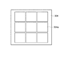
- FIG. 12 shows a plan view of the mask layer 304 used in creating the third second conductivity type region 35c.
- An opening 304 a is formed in the mask layer 304 .
- the area of the opening 304a is formed larger than the area of the opening 300a (see FIG. 6).
- step-112 is performed between step-100 (see FIG. 5) and step-102 (see FIG. 5). Note that Steps -106 to -108 are the same as those described above, so descriptions thereof will be omitted.
- a third second conductivity type region 35c having a second conductivity type different from the first conductivity type and reaching the photoelectric conversion layer 34 is formed.
- a mask layer 304 (see FIG. 10) is formed on the lower surface side of the second compound semiconductor layer 32, and, for example, impurities having the second conductivity type (p-type) (specifically zinc, Zn) are formed. ) can be vapor phase diffused or solid phase diffused to form the third second conductivity type region 35c. After that, the mask layer 300 is removed. After that, steps similar to step-102 (see FIG. 5) and step-104 (see FIG. 5) are performed.
- the spreading range of the multi-step Zn diffusion region, the impurity concentration, etc. are adjusted by changing the shape of the mask, impurity concentration, diffusion temperature, diffusion time, etc. It is possible.
- the first second-conductivity-type region 35a, the second second-conductivity-type region 35b, and the third second-conductivity-type region 35b are formed by three-stage Zn diffusion.
- a mold region 35c is formed. Since the third second-conductivity-type region 35c is further formed, holes, which are carriers generated on the incident light side of the photoelectric conversion layer 34, are also generated at the boundary of the first second-conductivity-type region 35a. Due to the electric field, it becomes possible to collect more by the second electrode 52, and it becomes possible to further suppress color mixture. As a result, carriers generated in a predetermined range (corresponding to the pixel range) above the second electrode 52 can be collected by the second electrode 52 within the same pixel.
- the photoelectric conversion element 101 of the imaging apparatus 100 according to the third embodiment differs from the imaging apparatus 100 according to the first embodiment in that the photoelectric conversion element 101 performs two stages of Zn diffusion from different locations. Differences from the imaging apparatus 100 according to the first embodiment will be described below.
- FIG. 13 is a schematic partial cross-sectional view of the photoelectric conversion element 101 according to the third embodiment.
- the photoelectric conversion element 101 differs from the photoelectric conversion element 101 according to the first embodiment in that it includes a fourth second-conductivity-type region 35d and a fifth second-conductivity-type region 35e in which Zn is diffused from different positions.
- FIG. 14 is a diagram showing the relationship between the position and concentration of the fourth second-conductivity-type region 35d and the fifth second-conductivity-type region 35e.
- the vertical axis indicates the concentration
- the horizontal axis indicates the position on the AA' line (see FIG. 13).
- the position of the lower surface of the second compound semiconductor layer 32 is indicated by 0 as the Zn diffusion surface, and the position from the Zn diffusion surface is indicated as the depth.
- a line L106 indicates the relationship between the depth of the fourth second conductivity type region 35d and the impurity concentration.
- a line L108 indicates the relationship between the depth of the fifth second conductivity type region 35e and the impurity concentration.
- a line L110 indicates the sum of the concentrations of the fourth second-conductivity-type region 35d and the fifth second-conductivity-type region 35e.
- FIG. 15 shows a plan view of the mask layer 306 used in creating the fifth second conductivity type region 35e.
- FIG. 16 is a schematic diagram showing a step of forming the fourth second-conductivity-type region 35d and the fifth second-conductivity-type region 35e. A doughnut-shaped opening 306 a is formed in the mask layer 306 .
- a fourth second conductivity type region 35d having a second conductivity type different from the first conductivity type and reaching the photoelectric conversion layer 34 is formed.
- a mask layer 302 (see FIG. 7) is formed on the lower surface side of the second compound semiconductor layer 32, and, for example, impurities having the second conductivity type (p-type) (specifically, zinc, Zn) are formed. ) is diffused in the vapor phase. In this case, vapor phase diffusion takes longer than in step 104 (see FIG. 5). After that, the mask layer 302 is removed.
- a fifth second conductivity type region 35e having a second conductivity type different from the first conductivity type and reaching the photoelectric conversion layer 34 is formed.
- a mask layer 306 (see FIG. 15) is formed on the lower surface side of the second compound semiconductor layer 32, and, for example, an impurity having a second conductivity type (p-type) (specifically, zinc, Zn) is formed. ) is diffused in the vapor phase. After that, the mask layer 302 is removed.
- p-type specifically, zinc, Zn
- the spread range of the multiple stages of Zn diffusion regions, the impurity concentration, etc. can be set with a higher degree of freedom. can be adjusted with
- the photoelectric conversion element 101 As described above, in the photoelectric conversion element 101 according to the present embodiment, two stages of Zn diffusion are performed from different locations to form the fourth second-conductivity-type region 35d and the fifth second-conductivity-type region 35e. be done. In this way, by diffusing Zn from different locations, it is possible to form a region in which the concentration distribution in the depth direction continuously decreases. Therefore, it is possible to freely set the density distribution, that is, the electric field, and to form an electric field that further prevents color mixture.
- the photoelectric conversion element 101 of the imaging device 100 according to the fourth embodiment differs from the imaging device 100 according to the first embodiment in that Zn diffusion is performed on the photoelectric conversion layer 34 having a laminated structure with different impurity concentrations in advance. do. Differences from the imaging apparatus 100 according to the first embodiment will be described below.
- FIG. 17 is a schematic partial cross-sectional view of the photoelectric conversion element 101 according to the fourth embodiment.
- the photoelectric conversion layer 34 according to the fourth embodiment is different from the photoelectric conversion element 101 according to the first embodiment in that it further includes a photoelectric conversion layer 38 having a different impurity concentration.
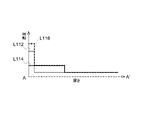
- FIG. 18 is a diagram showing the relationship between the position and concentration of the photoelectric conversion layer 34 having different impurity concentrations of the photoelectric conversion layer 38 and the second second conductivity type region 35b.
- the vertical axis indicates the concentration
- the horizontal axis indicates the position on the AA' line (see FIG. 13).
- the position of the lower surface of the second compound semiconductor layer 32 is indicated by 0 as the Zn diffusion surface, and the position from the Zn diffusion surface is indicated as the depth.
- a line L114 indicates the relationship between the depth of the photoelectric conversion layer 34 having the photoelectric conversion layer 38 and the impurity concentration.
- a line L112 indicates the relationship between the depth of the second second conductivity type region 35b and the impurity concentration.
- a line L116 indicates the sum of the concentrations of the photoelectric conversion layer 34 having the photoelectric conversion layer 38 and the second conductivity type region 35b.
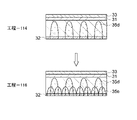
- FIG. 19A and 19B are diagrams for explaining an example of a method for manufacturing the photoelectric conversion element 101 according to the fourth embodiment. Note that Step-106 to Step-108 (see FIG. 8) are the same as those described above, so description thereof will be omitted.
- a second compound semiconductor layer 32 is formed sequentially.
- a deposition substrate made of InP and having a thickness of 0.1 ⁇ m to 1 ⁇ m is prepared.
- a first compound semiconductor layer 31 with a thickness of 0.1 ⁇ m to 1 ⁇ m, a photoelectric conversion layer 34 with a thickness of 2 ⁇ m to 5 ⁇ m, a photoelectric conversion layer 34 with a thickness of 1 ⁇ m to 3 ⁇ m, and a photoelectric conversion layer 34 with a thickness of 1 ⁇ m to 3 ⁇ m are formed on the deposition substrate.
- a conversion layer 38 and a second compound semiconductor layer 32 having a thickness of 0.1 ⁇ m to 1 ⁇ m are sequentially formed.
- Step-120 As shown in FIG. 19, after that, at least part of the second compound semiconductor layer 32 has a second conductivity type different from the first conductivity type, and a second second conductivity type region reaching the photoelectric conversion layer 38 is formed. 35b. More specifically, a mask layer 302 (see FIG. 7) is formed on the lower surface side of the second compound semiconductor layer 32, and, for example, impurities having the second conductivity type (p-type) (specifically, zinc, Zn) are formed. ) can be diffused in the vapor phase or solid phase to form the first second conductivity type region 35a. After that, the mask layer 300 is removed.
- p-type specifically, zinc, Zn
- the photoelectric conversion element 101 forms the first second conductivity type region 35a in the photoelectric conversion layer 34 having a laminated structure with different impurity concentrations in advance.
- the density distribution that is, the electric field can be set more freely, and an electric field that can prevent color mixture between pixels can be formed.
- the photoelectric conversion element 101 of the imaging device 100 according to the fifth embodiment performs Zn diffusion in multiple stages on the photoelectric conversion layer 34 having a laminated structure with different impurity concentrations in advance, which is different from that of the imaging device according to the first embodiment. Differs from 100. Differences from the imaging apparatus 100 according to the first embodiment will be described below.
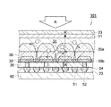
- FIG. 20 is a schematic partial cross-sectional view of the photoelectric conversion element 101 according to the fifth embodiment.
- the photoelectric conversion layer 34 according to the fifth embodiment is different from the photoelectric conversion element 101 according to the first embodiment in that it further includes a photoelectric conversion layer 38 having a different impurity concentration.
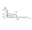
- FIG. 21 is a diagram showing the relationship between the position and concentration of the photoelectric conversion layer 34 having the photoelectric conversion layer 38, the first second-conductivity-type region 35a, and the second second-conductivity-type region 35b.
- the vertical axis indicates the concentration
- the horizontal axis indicates the position on the AA' line (see FIG. 13).
- the position of the lower surface of the second compound semiconductor layer 32 is indicated by 0 as the Zn diffusion surface, and the position from the Zn diffusion surface is indicated as the depth.
- a line L118 indicates the relationship between the depth of the photoelectric conversion layer 34 having the photoelectric conversion layer 38 and the impurity concentration.
- a line L120 indicates the relationship between the depth of the first second conductivity type region 35a and the impurity concentration.
- a line L122 indicates the relationship between the depth of the second second conductivity type region 35b and the impurity concentration.
- a line L124 indicates the sum of the concentrations of the photoelectric conversion layer 34 having the photoelectric conversion layer 38, the first second-conductivity-type region 35a, and the second second-conductivity-type region 35b.
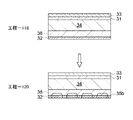
- FIG. 22 is a diagram illustrating an example of a method for manufacturing the photoelectric conversion element 101 according to the fifth embodiment. Note that Step-106 to Step-108 (see FIG. 8) are the same as those described above, so description thereof will be omitted.
- Step-118 After [Step-118], Step-122 and Step-124 are performed.
- Step-122 As shown in FIG. 22, after that, at least part of the second compound semiconductor layer 32 has a second conductivity type different from the first conductivity type, and a first second conductivity type region reaching the photoelectric conversion layer 34 is formed. 35a. More specifically, a mask layer 300 (see FIG. 6) is formed on the lower surface side of the second compound semiconductor layer 32, and, for example, impurities having the second conductivity type (p-type) (specifically, zinc, Zn) are formed. ) can be diffused in the vapor phase or solid phase to form the first second conductivity type region 35a. After that, the mask layer 300 is removed.
- impurities having the second conductivity type p-type
- impurities having the second conductivity type specifically, zinc, Zn
- Step-124 As shown in FIG. 22, the second second conductivity type region 35b having the second conductivity type and reaching the photoelectric conversion layer 34 is then formed. More specifically, a mask layer 302 (see FIG. 7) is formed on the lower surface side of the second compound semiconductor layer 32, and, for example, impurities having the second conductivity type (p-type) (specifically, zinc, Zn) are formed. ) can be diffused in the vapor phase or solid phase to form the second second conductivity type region 35b. For example, the concentration of Zn in step-124 is higher than that in step-122 and diffused at a higher temperature. After that, the mask layer 302 is removed.
- impurities having the second conductivity type p-type
- impurities having the second conductivity type specifically, zinc, Zn
- the concentration of Zn in step-124 is higher than that in step-122 and diffused at a higher temperature.
- the Zn diffusion regions are formed in multiple stages, by changing the shape of the mask, impurity concentration, temperature, time, etc., the spread range of the multiple stages of Zn diffusion regions, the impurity concentration, etc. can be changed. It is possible.
- the first second-conductivity-type region 35a and the second second-conductivity-type region 35a are added to the photoelectric conversion layer 34 having a laminated structure with different impurity concentrations in advance. Mold region 35b is formed.
- the density distribution that is, the electric field can be set more freely, and an electric field can be formed that can further prevent color mixture between pixels.
- FIG. 23 is a conceptual diagram showing an example in which the disclosed imaging device 100 (201 in FIG. 23) is used as an electronic device (camera) 200.
- the electronic device 200 has an imaging device 201 , an optical lens 210 , a shutter device 211 , a driving circuit 212 and a signal processing circuit 213 .
- the optical lens 210 forms an image of image light (incident light) from a subject on the imaging surface of the imaging device 201 .
- signal charges are accumulated in the imaging device 201 for a certain period of time.
- the shutter device 211 controls a light irradiation period and a light shielding period for the imaging device 201 .
- a drive circuit 212 supplies a drive signal for controlling the transfer operation of the imaging device 201 and the shutter operation of the shutter device 211 .
- Signal transfer of the imaging device 201 is performed by a driving signal (timing signal) supplied from the driving circuit 212 .
- the signal processing circuit 213 performs various signal processing.
- the video signal that has undergone signal processing is stored in a storage medium such as a memory, or is output to a monitor.
- the pixel size can be reduced in the imaging device 201, and the transfer efficiency can be improved, so that the electronic device 200 with improved pixel characteristics can be obtained.
- the electronic device 200 to which the imaging device 201 can be applied is not limited to cameras, and can be applied to imaging devices such as digital still cameras and camera modules for mobile devices such as mobile phones.
- this technique can take the following structures. (1) a first compound semiconductor layer made of a first compound semiconductor material having a first conductivity type; a photoelectric conversion layer formed in contact with the first compound semiconductor layer; a second compound semiconductor layer formed in contact with the photoelectric conversion layer and made of a second compound semiconductor material having the first conductivity type; a first second conductivity type region formed in at least part of the second compound semiconductor layer, having a second conductivity type different from the first conductivity type, and reaching the photoelectric conversion layer; a second second-conductivity-type region formed in at least a portion of the second compound semiconductor layer, having the second conductivity type, and reaching the photoelectric conversion layer, the first second-conductivity-type region being formed in at least a portion of the second compound semiconductor layer; a second second conductivity type region having a region different from A photoelectric conversion element.
- the photoelectric conversion element according to (1) further comprising:
- the first second conductivity type region has a lower impurity concentration than the second second conductivity type region, and the first second conductivity type region has the second conductivity type.
- the photoelectric conversion element according to (3) which is formed closer to the first compound semiconductor layer than the region.
- the first second-conductivity-type region has a higher impurity concentration than the second second-conductivity-type region, and the first compound semiconductor layer has a higher impurity concentration than the second second-conductivity-type region.
- the photoelectric conversion element according to (7) which is formed up to near.
- the photoelectric conversion layer is made of InGaAs;
- the photoelectric conversion element according to (13), wherein the first compound semiconductor layer and the second compound semiconductor layer are made of InP.
- a method for manufacturing a photoelectric conversion element comprising steps.
- At least one of impurity concentration, temperature, and time is different between the state of diffusing impurities through the first mask layer and the state of diffusing impurities through the second mask layer, ( 19) The method for producing a photoelectric conversion element according to 19).
- first compound semiconductor layer 32: second compound semiconductor layer
- 34 photoelectric conversion layer
- 35a to 35e second conductivity type region
- 51 first electrode
- 52 second electrode
- 60 drive substrate
- 100 imaging device
- 101 photoelectric conversion element (imaging element).
Landscapes
- Solid State Image Pick-Up Elements (AREA)
- Light Receiving Elements (AREA)
Abstract
Description
前記第1化合物半導体層に接して形成される光電変換層と、
前記光電変換層に接して形成され、前記第1導電型を有する第2化合物半導体材料から成る第2化合物半導体層と、
少なくとも前記第2化合物半導体層の一部に形成され、前記第1導電型とは異なる第2導電型を有し、前記光電変換層に達する第1の第2導電型領域と、
少なくとも前記第2化合物半導体層の一部に形成され、前記第2導電型を有し、前記光電変換層に達する第2の第2導電型領域であって、前記第1の第2導電型領域と異なる領域を有する第2の第2導電型領域と、
を備える、光電変換素子が提供される。
前記第2導電型領域上に形成される第2電極と、
を、更に備えてもよい。
前記第1化合物半導体層、及び前記第2化合物半導体層はInPから成ってもよい。
を、順次、形成し、
少なくとも第2化合物半導体層の一部に、第1導電型とは異なる第2導電型を有し、光電変換層に達する第1の第2導電型領域を形成し、
前記第1の第2導電型領域と異なる条件により、少なくとも第2化合物半導体層の一部に、前記第2導電型を有し、前記光電変換層に達する第2の第2導電型領域を形成する、 各工程を備えた光電変換素子の製造方法が提供される。
図1は、本技術の第1実施形態における撮像装置100の構成例を示す図である。図1に示すように、撮像装置100は、光電変換素子101が2次元マトリクス状(2次元アレイ状)に配列された撮像領域111、並びに、その駆動回路(周辺回路)としての垂直駆動回路112、カラム信号処理回路113、水平駆動回路114、出力回路115及び駆動制御回路116等から構成されている。尚、これらの回路は周知の回路から構成することができるし、また、他の回路構成(例えば、従来のCCD型撮像装置やCMOS型撮像装置にて用いられる各種の回路)を用いて構成することができることが可能である。すなわち、この撮像装置100は、複数段のZn拡散領域により光電変換素子101内に電界を生じさせ、画素間の混色の抑制をさせることが可能である。
図5に示すように、第1導電型を有する第1化合物半導体材料から成る第1化合物半導体層31、光電変換層34、及び、第1導電型を有する第2化合物半導体材料から成る第2化合物半導体層32を、順次、形成する。具体的には、InPから成り、厚さ0.1μm乃至1μmの成膜用基板を準備する。そして、周知のMOCVD法に基づき、成膜用基板の上に、厚さ0.1μm乃至1μmの第1化合物半導体層31、厚さ3μm乃至5μmの光電変換層34、厚さ0.1μm乃至1μmの第2化合物半導体層32を、順次、成膜する。
図5に示すように、その後、少なくとも第2化合物半導体層32の一部に、第1導電型とは異なる第2導電型を有し、光電変換層34に達する第1の第2導電型領域35aを形成する。より具体的には、第2化合物半導体層32の下面側にマスク層300(図6参照)を形成し、例えば、第2導電型(p型)を有する不純物(具体的には、亜鉛、Zn)を気相拡散させ、あるいは、固相拡散させることで、第1の第2導電型領域35aを形成することができる。その後、マスク層300を除去する。
図5に示すように、その後、第2導電型を有し、光電変換層34に達する第2の第2導電型領域35bを形成する。より具体的には、第2化合物半導体層32の下面側にマスク層302(図7参照)を形成し、例えば、第2導電型(p型)を有する不純物(具体的には、亜鉛、Zn)を気相拡散させ、あるいは、固相拡散させることで、第2の第2導電型領域35bを形成することができる。例えば、工程-102のZnの濃度よりも工程-104の濃度を高くし、より高温で拡散させる。その後、マスク層302を除去する。このように、複数段のZn拡散領域を生成する場合には、マスクの形状、不純物の濃度、拡散温度、及び拡散時間等を変えることにより、複数段のZn拡散領域の広がり範囲、不純物濃度などを変更可能である。
工程-104の後、工程-106~工程-108により第2の第2導電型領域35bに第2電極52を形成する。併せて、第1化合物半導体層31に電気的に接続された第1電極51を形成する。
[工程-106]
より詳細には、第2の第2導電型領域35b及び第2化合物半導体層32の上にSiNから成る被覆層36を形成し、次いで、フォトリソグラフィ技術及びエッチング技術に基づき、第2電極52を形成すべき部分の被覆層36に開口部36Aを形成する
次に、開口部36Aの底部に露出した第2導電型領域35の上から被覆層36の上に亙り第2電極52を形成し、被覆層36の上に亙り第1電極51を形成する。
次に、支持基板23と駆動用基板60とを、絶縁膜24を介して周知の方法に基づき貼り合わせる。こうして、図2に示す構造の光電変換素子101を構成することができる。なお、第1電極51及び第2電極52の頂面には、接続部として銅層(図示せず)を形成しておく。
第2実施形態に係る撮像装置100の光電変換素子101は、光電変換素子101は、3段階の不純物拡散により、更に第3の第2導電型領域35cを備える点で、第1実施形態に係る撮像装置100と相違する。以下では、第1実施形態に係る撮像装置100と相違する点を説明する。
図11に示すように、少なくとも第2化合物半導体層32の一部に、第1導電型とは異なる第2導電型を有し、光電変換層34に達する第3の第2導電型領域35cを形成する。より具体的には、第2化合物半導体層32の下面側にマスク層304(図10参照)を形成し、例えば、第2導電型(p型)を有する不純物(具体的には、亜鉛、Zn)を気相拡散させ、あるいは又、固相拡散させることで、第3の第2導電型領域35cを形成することができる。その後、マスク層300を除去する。その後工程-102(図5参照)、工程-104(図5参照)と同様の工程を行う。なお、複数段のZn拡散領域を生成する場合には、マスクの形状、不純物の濃度、拡散温度、及び拡散時間等を変えることにより、複数段のZn拡散領域の広がり範囲、不純物濃度などを調整可能である。
第3実施形態に係る撮像装置100の光電変換素子101は、光電変換素子101は、2段階のZn拡散を異なる場所から行う点で、第1実施形態に係る撮像装置100と相違する。以下では、第1実施形態に係る撮像装置100と相違する点を説明する。
図16に示すように、少なくとも第2化合物半導体層32の一部に、第1導電型とは異なる第2導電型を有し、光電変換層34に達する第4の第2導電型領域35dを形成する。より具体的には、第2化合物半導体層32の下面側にマスク層302(図7参照)を形成し、例えば、第2導電型(p型)を有する不純物(具体的には、亜鉛、Zn)を気相拡散させる。この場合、工程104(図5参照)よりも長い時間で気相拡散させる。その後、マスク層302を除去する。
図16に示すように、少なくとも第2化合物半導体層32の一部に、第1導電型とは異なる第2導電型を有し、光電変換層34に達する第5の第2導電型領域35eを形成する。より具体的には、第2化合物半導体層32の下面側にマスク層306(図15参照)を形成し、例えば、第2導電型(p型)を有する不純物(具体的には、亜鉛、Zn)を気相拡散させる。その後、マスク層302を除去する。なお、複数段のZn拡散領域を生成する場合には、不純物の濃度、拡散温度、及び拡散時間等を変えることにより、複数段のZn拡散領域の広がり範囲、及び不純物濃度などをより高い自由度をもって調整可能である。
第4実施形態に係る撮像装置100の光電変換素子101は、不純物濃度が予め異なる積層構造を有する光電変換層34に対してZn拡散を行う点で、第1実施形態に係る撮像装置100と相違する。以下では、第1実施形態に係る撮像装置100と相違する点を説明する。
図19に示すように、第1導電型を有する第1化合物半導体材料から成る第1化合物半導体層31、光電変換層34、光電変換層38及び、第1導電型を有する第2化合物半導体材料から成る第2化合物半導体層32を、順次、形成する。具体的には、InPから成り、厚さ0.1μm乃至1μmの成膜用基板を準備する。そして、周知のMOCVD法に基づき、成膜用基板の上に、厚さ0.1μm乃至1μmの第1化合物半導体層31、厚さ2μm乃至5μmの光電変換層34、厚さ1μm乃至3μmの光電変換層38、厚さ0.1μm乃至1μmの第2化合物半導体層32を、順次、成膜する。
図19に示すように、その後、少なくとも第2化合物半導体層32の一部に、第1導電型とは異なる第2導電型を有し、光電変換層38に達する第2の第2導電型領域35bを形成する。より具体的には、第2化合物半導体層32の下面側にマスク層302(図7参照)を形成し、例えば、第2導電型(p型)を有する不純物(具体的には、亜鉛、Zn)を気相拡散させ、あるいは又、固相拡散させることで、第1の第2導電型領域35aを形成することができる。その後、マスク層300を除去する。
第5実施形態に係る撮像装置100の光電変換素子101は、不純物濃度が予め異なる積層構造を有する光電変換層34に対して複数段のZn拡散を行う点で、第1実施形態に係る撮像装置100と相違する。以下では、第1実施形態に係る撮像装置100と相違する点を説明する。
図22に示すように、その後、少なくとも第2化合物半導体層32の一部に、第1導電型とは異なる第2導電型を有し、光電変換層34に達する第1の第2導電型領域35aを形成する。より具体的には、第2化合物半導体層32の下面側にマスク層300(図6参照)を形成し、例えば、第2導電型(p型)を有する不純物(具体的には、亜鉛、Zn)を気相拡散させ、あるいは又、固相拡散させることで、第1の第2導電型領域35aを形成することができる。その後、マスク層300を除去する。
図22に示すように、その後、第2導電型を有し、光電変換層34に達する第2の第2導電型領域35bを形成する。より具体的には、第2化合物半導体層32の下面側にマスク層302(図7参照)を形成し、例えば、第2導電型(p型)を有する不純物(具体的には、亜鉛、Zn)を気相拡散させ、あるいは又、固相拡散させることで、第2の第2導電型領域35bを形成することができる。例えば、工程-122のZnの濃度よりも工程-124の濃度を高くし、より高温で拡散させる。その後、マスク層302を除去する。このように、複数段のZn拡散領域を生成する場合には、マスクの形状、不純物の濃度、温度、及び時間等を変えることにより、複数段のZn拡散領域の広がり範囲、不純物濃度などを変更可能である。
(1)第1導電型を有する第1化合物半導体材料から成る第1化合物半導体層と、
前記第1化合物半導体層に接して形成される光電変換層と、
前記光電変換層に接して形成され、前記第1導電型を有する第2化合物半導体材料から成る第2化合物半導体層と、
少なくとも前記第2化合物半導体層の一部に形成され、前記第1導電型とは異なる第2導電型を有し、前記光電変換層に達する第1の第2導電型領域と、
少なくとも前記第2化合物半導体層の一部に形成され、前記第2導電型を有し、前記光電変換層に達する第2の第2導電型領域であって、前記第1の第2導電型領域と異なる領域を有する第2の第2導電型領域と、
を備える、光電変換素子。
前記第2導電型領域上に形成される第2電極と、
を、更に備える、(1)に記載の光電変換素子。
更に備える、(4)に記載の光電変換素子。
前記第1化合物半導体層、及び前記第2化合物半導体層はInPから成る、(13)に記載の光電変換素子。
少なくとも第2化合物半導体層の一部に、第1導電型とは異なる第2導電型を有し、光電変換層に達する第1の第2導電型領域を形成し、
前記第1の第2導電型領域と異なる条件により、少なくとも第2化合物半導体層の一部に、前記第2導電型を有し、前記光電変換層に達する第2の第2導電型領域を形成する、 各工程を備えた光電変換素子の製造方法。
Claims (20)
- 第1導電型を有する第1化合物半導体材料から成る第1化合物半導体層と、
前記第1化合物半導体層に接して形成される光電変換層と、
前記光電変換層に接して形成され、前記第1導電型を有する第2化合物半導体材料から成る第2化合物半導体層と、
少なくとも前記第2化合物半導体層の一部に形成され、前記第1導電型とは異なる第2導電型を有し、前記光電変換層に達する第1の第2導電型領域と、
少なくとも前記第2化合物半導体層の一部に形成され、前記第2導電型を有し、前記光電変換層に達する第2の第2導電型領域であって、前記第1の第2導電型領域と異なる領域を有する第2の第2導電型領域と、
を備える、光電変換素子。 - 前記第1化合物半導体層に電気的に接続される第1電極と、
前記第2導電型領域上に形成される第2電極と、
を、更に備える、請求項1に記載の光電変換素子。 - 前記第1の第2導電型領域と前記第2の第2導電型領域とは、不純物濃度が異なる、請求項1に記載の光電変換素子。
- 前記第1の第2導電型領域の方が前記第2の第2導電型領域よりも不純物濃度が低く、前記第1の第2導電型領域は、前記第2の第2導電型領域よりも前記第1化合物半導体層のより近くまで形成される、請求項3に記載の光電変換素子。
- 少なくとも前記第2化合物半導体層の一部に形成され、前記第2導電型を有し、前記光電変換層に達する第3の第2導電型領域であって、前記第1の第2導電型領域、及び前記第2の第2導電型領域と異なる領域を有する第3の第2導電型領域を、
更に備える、請求項4に記載の光電変換素子。 - 前記第1の第2導電型領域と前記第2の第2導電型領域とは、異なる条件で不純物が拡散され、形成される、請求項1に記載の光電変換素子。
- 前記第1の第2導電型領域と前記第2の第2導電型領域とは、異なる位置から前記不純物が拡散され、形成される、請求項6に記載の光電変換素子。
- 前記第1の第2導電型領域の方が前記第2の第2導電型領域よりも不純物濃度が高く、前記第2の第2導電型領域よりも前記第1化合物半導体層のより近くまで形成される、請求項7に記載の光電変換素子。
- 前記第2の第2導電型領域は、前記第2化合物半導体層に沿って2つの凸状領域を有する、請求項8に記載の光電変換素子。
- 前記光電変換層は、複数の不純物濃度の異なる層が積層される、請求項1に記載の光電変換素子。
- 前記第1電極は、前記第1化合物半導体層の光入射側の面上に形成されている、請求項2に記載の光電変換素子。
- 前記第1化合物半導体層、及び前記第2化合物半導体層は、同じ材料から成る、請求項1に記載の光電変換素子。
- 前記第1化合物半導体層、及び前記第2化合物半導体層は、III-V属化合物半導体材料から成る、請求項12に記載の光電変換素子。
- 前記光電変換層はInGaAsから成り、
前記第1化合物半導体層、及び前記第2化合物半導体層はInPから成る、請求項13に記載の光電変換素子。 - 前記第1化合物半導体層を介して光が入射する、請求項1に記載の光電変換素子。
- 請求項1に記載の光電変換素子が、複数、2次元マトリクス状に配列される、撮像装置。
- 第1導電型を有する第1化合物半導体材料から成る第1化合物半導体層、光電変換層、及び、第1導電型を有する第2化合物半導体材料から成る第2化合物半導体層、
を、順次、形成し、
少なくとも第2化合物半導体層の一部に、第1導電型とは異なる第2導電型を有し、光電変換層に達する第1の第2導電型領域を形成し、
前記第1の第2導電型領域と異なる条件により、少なくとも第2化合物半導体層の一部に、前記第2導電型を有し、前記光電変換層に達する第2の第2導電型領域を形成する、 各工程を備えた光電変換素子の製造方法。 - 前記第2化合物半導体層からマスク層を介して不純物を拡散させ、前記第1の第2導電型領域及び前記第2の第2導電型領域を形成する、請求項17に記載の光電変換素子の製造方法。
- 前記第2化合物半導体層から第1マスク層を介して不純物を拡散させ、前記第1マスク層を削除した後に第2マスク層を介して不純物を拡散させ、前記第2の第2導電型領域を形成する、請求項18に記載の光電変換素子の製造方法。
- 前記第1マスク層を介して不純物を拡散させる状態と、前記第2マスク層を介して不純物を拡散さる状態と、は不純物の濃度、温度、及び時間の少なくともいずれかが異なる、請求項19に記載の光電変換素子の製造方法。
Priority Applications (2)
| Application Number | Priority Date | Filing Date | Title |
|---|---|---|---|
| US18/550,419 US20240194807A1 (en) | 2021-03-25 | 2022-02-17 | Photoelectric conversion element, method for manufacturing the same, and imaging device |
| JP2023508794A JPWO2022202006A1 (ja) | 2021-03-25 | 2022-02-17 |
Applications Claiming Priority (2)
| Application Number | Priority Date | Filing Date | Title |
|---|---|---|---|
| JP2021-051422 | 2021-03-25 | ||
| JP2021051422 | 2021-03-25 |
Publications (1)
| Publication Number | Publication Date |
|---|---|
| WO2022202006A1 true WO2022202006A1 (ja) | 2022-09-29 |
Family
ID=83396832
Family Applications (1)
| Application Number | Title | Priority Date | Filing Date |
|---|---|---|---|
| PCT/JP2022/006473 Ceased WO2022202006A1 (ja) | 2021-03-25 | 2022-02-17 | 光電変換素子及びその製造方法並びに撮像装置 |
Country Status (3)
| Country | Link |
|---|---|
| US (1) | US20240194807A1 (ja) |
| JP (1) | JPWO2022202006A1 (ja) |
| WO (1) | WO2022202006A1 (ja) |
Citations (7)
| Publication number | Priority date | Publication date | Assignee | Title |
|---|---|---|---|---|
| JPH0382084A (ja) * | 1989-08-24 | 1991-04-08 | Mitsubishi Electric Corp | 半導体受光素子 |
| JPH05160426A (ja) * | 1991-12-06 | 1993-06-25 | Nec Corp | 半導体受光素子 |
| JP2007184410A (ja) * | 2006-01-06 | 2007-07-19 | Sumitomo Electric Ind Ltd | 半導体受光素子およびその製造方法 |
| JP2010098239A (ja) * | 2008-10-20 | 2010-04-30 | Nec Electronics Corp | 光半導体装置及び光半導体装置の製造方法 |
| JP2012160691A (ja) * | 2011-01-14 | 2012-08-23 | Sumitomo Electric Ind Ltd | 受光装置、光学装置および受光装置の製造方法 |
| US20150171256A1 (en) * | 2013-01-24 | 2015-06-18 | Osi Optoelectronics, Inc. | Shallow Junction Photodiode for Detecting Short Wavelength Light |
| JP2017175102A (ja) * | 2016-03-16 | 2017-09-28 | ソニー株式会社 | 光電変換素子及びその製造方法並びに撮像装置 |
-
2022
- 2022-02-17 US US18/550,419 patent/US20240194807A1/en active Pending
- 2022-02-17 JP JP2023508794A patent/JPWO2022202006A1/ja active Pending
- 2022-02-17 WO PCT/JP2022/006473 patent/WO2022202006A1/ja not_active Ceased
Patent Citations (7)
| Publication number | Priority date | Publication date | Assignee | Title |
|---|---|---|---|---|
| JPH0382084A (ja) * | 1989-08-24 | 1991-04-08 | Mitsubishi Electric Corp | 半導体受光素子 |
| JPH05160426A (ja) * | 1991-12-06 | 1993-06-25 | Nec Corp | 半導体受光素子 |
| JP2007184410A (ja) * | 2006-01-06 | 2007-07-19 | Sumitomo Electric Ind Ltd | 半導体受光素子およびその製造方法 |
| JP2010098239A (ja) * | 2008-10-20 | 2010-04-30 | Nec Electronics Corp | 光半導体装置及び光半導体装置の製造方法 |
| JP2012160691A (ja) * | 2011-01-14 | 2012-08-23 | Sumitomo Electric Ind Ltd | 受光装置、光学装置および受光装置の製造方法 |
| US20150171256A1 (en) * | 2013-01-24 | 2015-06-18 | Osi Optoelectronics, Inc. | Shallow Junction Photodiode for Detecting Short Wavelength Light |
| JP2017175102A (ja) * | 2016-03-16 | 2017-09-28 | ソニー株式会社 | 光電変換素子及びその製造方法並びに撮像装置 |
Also Published As
| Publication number | Publication date |
|---|---|
| US20240194807A1 (en) | 2024-06-13 |
| JPWO2022202006A1 (ja) | 2022-09-29 |
Similar Documents
| Publication | Publication Date | Title |
|---|---|---|
| JP4799594B2 (ja) | 固体撮像装置およびその製造方法 | |
| US9117728B2 (en) | Solid-state imaging device, method of manufacturing same, and electronic apparatus | |
| CN103117289B (zh) | 固体摄像元件、固体摄像元件制造方法和电子设备 | |
| CN104981906B (zh) | 固态图像传感器、其制造方法和电子设备 | |
| TWI725484B (zh) | 固態成像裝置,用於製造固態成像裝置的方法和電子設備 | |
| US8817152B2 (en) | Solid-state imaging device, camera, and electronic device | |
| US20160218138A1 (en) | Solid-state image pickup device and method for manufacturing a solid-state image pickup device | |
| US20110042552A1 (en) | Solid-state imaging device and method of manufacturing the same | |
| JP2012164768A (ja) | 固体撮像装置 | |
| CN103688359B (zh) | 固态成像装置及其驱动方法、固态成像装置的制造方法以及电子信息设备 | |
| WO2021117523A1 (ja) | 固体撮像素子及び電子機器 | |
| US20140151753A1 (en) | Solid-state imaging apparatus, manufacturing method thereof, and electronic information device | |
| JP2001094086A (ja) | 光電変換装置及びその製造方法 | |
| Scott-Thomas | Trends and developments in state-of-the-art cmos image sensors | |
| JP2015220255A (ja) | 裏面照射型cmos型撮像素子、及び、裏面照射型cmos型撮像素子の製造方法 | |
| JP2015012074A (ja) | 固体撮像装置および固体撮像装置の製造方法 | |
| CN100565890C (zh) | 摄像装置 | |
| US9876041B2 (en) | Solid-state imaging device and method of manufacturing the same | |
| KR102242580B1 (ko) | 이미지 센서 및 이의 제조 방법 | |
| WO2022202006A1 (ja) | 光電変換素子及びその製造方法並びに撮像装置 | |
| JP7172389B2 (ja) | 撮像素子、撮像装置、及び、撮像素子の製造方法 | |
| CN117957659A (zh) | 一种固态成像设备以及一种电子装置 | |
| JP2013211295A (ja) | 固体撮像装置及びその製造方法、電子機器 |
Legal Events
| Date | Code | Title | Description |
|---|---|---|---|
| 121 | Ep: the epo has been informed by wipo that ep was designated in this application |
Ref document number: 22774806 Country of ref document: EP Kind code of ref document: A1 |
|
| WWE | Wipo information: entry into national phase |
Ref document number: 2023508794 Country of ref document: JP |
|
| WWE | Wipo information: entry into national phase |
Ref document number: 18550419 Country of ref document: US |
|
| NENP | Non-entry into the national phase |
Ref country code: DE |
|
| 122 | Ep: pct application non-entry in european phase |
Ref document number: 22774806 Country of ref document: EP Kind code of ref document: A1 |