WO2022202003A1 - 半導体装置及び半導体モジュール - Google Patents
半導体装置及び半導体モジュール Download PDFInfo
- Publication number
- WO2022202003A1 WO2022202003A1 PCT/JP2022/006453 JP2022006453W WO2022202003A1 WO 2022202003 A1 WO2022202003 A1 WO 2022202003A1 JP 2022006453 W JP2022006453 W JP 2022006453W WO 2022202003 A1 WO2022202003 A1 WO 2022202003A1
- Authority
- WO
- WIPO (PCT)
- Prior art keywords
- cells
- conductor
- semiconductor device
- substrate
- cell
- Prior art date
- Legal status (The legal status is an assumption and is not a legal conclusion. Google has not performed a legal analysis and makes no representation as to the accuracy of the status listed.)
- Ceased
Links
Images



Classifications
-
- H—ELECTRICITY
- H10—SEMICONDUCTOR DEVICES; ELECTRIC SOLID-STATE DEVICES NOT OTHERWISE PROVIDED FOR
- H10D—INORGANIC ELECTRIC SEMICONDUCTOR DEVICES
- H10D10/00—Bipolar junction transistors [BJT]
- H10D10/01—Manufacture or treatment
-
- H—ELECTRICITY
- H10—SEMICONDUCTOR DEVICES; ELECTRIC SOLID-STATE DEVICES NOT OTHERWISE PROVIDED FOR
- H10D—INORGANIC ELECTRIC SEMICONDUCTOR DEVICES
- H10D10/00—Bipolar junction transistors [BJT]
- H10D10/80—Heterojunction BJTs
-
- H—ELECTRICITY
- H10—SEMICONDUCTOR DEVICES; ELECTRIC SOLID-STATE DEVICES NOT OTHERWISE PROVIDED FOR
- H10D—INORGANIC ELECTRIC SEMICONDUCTOR DEVICES
- H10D84/00—Integrated devices formed in or on semiconductor substrates that comprise only semiconducting layers, e.g. on Si wafers or on GaAs-on-Si wafers
-
- H—ELECTRICITY
- H10—SEMICONDUCTOR DEVICES; ELECTRIC SOLID-STATE DEVICES NOT OTHERWISE PROVIDED FOR
- H10D—INORGANIC ELECTRIC SEMICONDUCTOR DEVICES
- H10D84/00—Integrated devices formed in or on semiconductor substrates that comprise only semiconducting layers, e.g. on Si wafers or on GaAs-on-Si wafers
- H10D84/01—Manufacture or treatment
- H10D84/0112—Integrating together multiple components covered by H10D8/00, H10D10/00 or H10D18/00, e.g. integrating multiple BJTs
-
- H—ELECTRICITY
- H10—SEMICONDUCTOR DEVICES; ELECTRIC SOLID-STATE DEVICES NOT OTHERWISE PROVIDED FOR
- H10D—INORGANIC ELECTRIC SEMICONDUCTOR DEVICES
- H10D84/00—Integrated devices formed in or on semiconductor substrates that comprise only semiconducting layers, e.g. on Si wafers or on GaAs-on-Si wafers
- H10D84/01—Manufacture or treatment
- H10D84/02—Manufacture or treatment characterised by using material-based technologies
- H10D84/03—Manufacture or treatment characterised by using material-based technologies using Group IV technology, e.g. silicon technology or silicon-carbide [SiC] technology
- H10D84/038—Manufacture or treatment characterised by using material-based technologies using Group IV technology, e.g. silicon technology or silicon-carbide [SiC] technology using silicon technology, e.g. SiGe
Definitions
- the present invention relates to semiconductor devices and semiconductor modules including bipolar transistors.
- the emitter fingers are elongated from the periphery to the center of the chip under the condition that the area is constant. Also, when the emitter ballast resistor is provided, it is relatively high in the chip peripheral portion and relatively low in the central portion.
- a plurality of emitter fingers are each connected to a common emitter bonding pad through an emitter ballast resistor.
- a collector electrode and a base electrode are connected to a collector bonding pad and a base bonding pad, respectively.
- the heat generated by the emitter fingers diffuses in the thickness direction and in-plane direction of the substrate. Since the peripheral length of the emitter fingers in the central portion is longer than that of the emitter fingers in the chip peripheral portion, the central emitter fingers have higher heat dissipation characteristics in the in-plane direction.
- the heat diffused in the thickness direction and the in-plane direction of the substrate is finally conducted to a package or the like in which the semiconductor device is accommodated.
- An object of the present invention is to provide a semiconductor device that is less likely to be destroyed by thermal runaway.
- a substrate a plurality of three or more cells arranged side by side in a first direction on the substrate; a conductor protrusion disposed on the substrate and protruding away from the substrate; each of the plurality of cells, a bipolar transistor including a collector layer, a base layer, and an emitter layer; a ballast resistive element connected to the bipolar transistor; the conductor protrusions are connected to emitter layers of the bipolar transistors of the plurality of cells; the bipolar transistors of the plurality of cells are connected in parallel with each other; a semiconductor device in which the resistance value of the ballast resistance element included in the first cell at the end portion of the plurality of cells is greater than the resistance value of the ballast resistance element included in at least one second cell other than the end portion provided.
- a semiconductor device including a substrate, a plurality of cells of three or more arranged in a first direction on the substrate, and a conductor projection arranged on the substrate and protruding away from the substrate;
- the semiconductor device comprises a module substrate flip-chip mounted via the conductor projections, each of the plurality of cells includes a bipolar transistor including a collector layer, a base layer, and an emitter layer; the bipolar transistors of the plurality of cells are connected in parallel with each other; the conductor projection overlaps the plurality of cells in plan view and is electrically connected to emitter layers of the bipolar transistors of the plurality of cells;
- the module substrate is including a through via that overlaps with the conductor projection in a plan view, is elongated in the first direction, and is electrically connected to the conductor projection;
- the semiconductor module is provided, wherein the through via includes a portion wider than the width of the central portion at a location shifted from the central portion toward the end of the range in which the plurality of cells are
- a semiconductor device including a substrate, a plurality of cells of three or more arranged in a first direction on the substrate, and a conductor projection arranged on the substrate and protruding away from the substrate;
- the semiconductor device comprises a module substrate flip-chip mounted via the conductor projections, each of the plurality of cells includes a bipolar transistor including a collector layer, a base layer, and an emitter layer; the bipolar transistors of the plurality of cells are connected in parallel with each other; the conductor projection overlaps the plurality of cells in plan view and is electrically connected to emitter layers of the bipolar transistors of the plurality of cells;
- the module substrate is including at least two through vias that overlap the conductor projection in plan view, are electrically connected to the conductor projection, and are arranged side by side in the first direction;
- a semiconductor module is provided in which the through via is not arranged in the central portion of the range where the plurality of cells are arranged in the first direction.
- the second cells other than both ends are more easily destroyed than the first cells at both ends.
- the resistance value of the ballast resistance element included in the first cell greater than the resistance value of the ballast resistance element included in the second cell, a relatively large current flows through the second cell, resulting in a large amount of heat generation. Therefore, it is possible to suppress deterioration of the breakdown resistance of the second cell during low-temperature operation.
- the heat dissipation characteristics of the cells in the central portion are relatively lowered, and the temperature tends to rise. Therefore, it is possible to suppress deterioration of the breakdown resistance of the second cell during low-temperature operation.
- FIG. 1 is an equivalent circuit diagram of the semiconductor device according to the first embodiment.
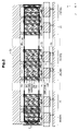
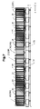
- FIG. 2 is a schematic plan view of the semiconductor device according to the first embodiment.
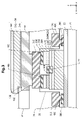
- FIG. 3 is a cross-sectional view taken along dashed-dotted line 3-3 in FIG.
- FIG. 4 is a graph showing measurement results of the rupture boundary of a semiconductor device in which the resistance value of the base ballast resistance element is the same in all cells.
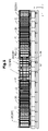
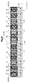
- FIG. 5 is a schematic plan view of a semiconductor device according to a second embodiment.
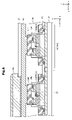
- FIG. 6 is a cross-sectional view taken along dashed-dotted line 6-6 in FIG.
- FIG. 7 is a schematic plan view of a semiconductor device according to a third embodiment.
- FIG. 8 is a schematic plan view of a semiconductor device according to a fourth embodiment.
- FIG. 1 is an equivalent circuit diagram of the semiconductor device according to the first embodiment.
- FIG. 2 is a schematic plan view of the semiconductor device according to the first embodiment.
- FIG. 3 is a cross-sectional view
- FIG. 9 is a schematic plan view of a semiconductor device according to a fifth embodiment.
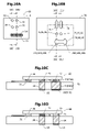
- FIG. 10A is a plan view showing the layout of main components of a semiconductor device included in a semiconductor module according to the sixth embodiment, and FIG. 10B shows the plan view of the main components of a module substrate.
- 10C and 10D are schematic cross-sectional views of a semiconductor module according to a sixth embodiment.
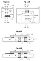
- 11A is a plan view showing the layout of main components of a semiconductor device included in a semiconductor module according to the seventh embodiment, and FIG. 11B shows the plan view of the main components of a module substrate.
- 11C and 11D are schematic cross-sectional views of a semiconductor module according to a seventh embodiment.
- FIG. 1 is an equivalent circuit diagram of the semiconductor device according to the first embodiment.
- the semiconductor device according to the first embodiment includes multiple cells 20 .
- a plurality of cells 20 are arranged in one direction on the substrate to form a cell row.
- aligned in one direction does not necessarily mean aligned in a straight line, and may be aligned in a zigzag pattern, for example.
- FIG. 1 shows two cells 20A located at both ends of a cell row, two cells 20 located one inside from both ends, and two cells 20B located in the center of the cell row.
- Each of the plurality of cells 20 includes a bipolar transistor 21, a base ballast resistive element 22, and an input capacitor 23.
- the bipolar transistors 21 of multiple cells 20 are connected in parallel with each other.
- the bipolar transistor 21 has its emitter connected to the emitter common wiring 50 and its collector connected to the collector common wiring 51 .
- the bipolar transistors 21 of the plurality of cells 20 are connected to a base bias wiring 52 common to the plurality of cells 20 via base ballast resistance elements 22, respectively, and are common to the plurality of cells 20 via an input capacitor 23. is connected to the high-frequency signal input wiring 53 of .
- a base bias current is supplied to the bipolar transistor 21 through the common base bias wiring 52 and the base ballast resistance element 22 for each cell 20 .
- the resistance value of the base ballast resistance element 22 included in the end cell 20A is greater than the resistance value of the base ballast resistance element 22 included in at least one cell 20B other than the end cells.
- a high frequency signal is input to the bipolar transistor 21 through the high frequency signal input wiring 53 and the input capacitor 23 for each cell 20 .
- a high frequency signal amplified by the bipolar transistor 21 is output from the common collector wiring 51 .
- a collector voltage is applied to the bipolar transistor 21 through the choke coil and collector common wiring 51 .
- FIG. 2 is a schematic plan view of the semiconductor device according to the first embodiment.
- a plurality of cells 20 are arranged side by side in one direction.
- An xyz orthogonal coordinate system is defined in which the y direction is the direction in which the plurality of cells 20 are arranged and the z direction is the normal direction of the surface of the substrate.
- An n-type conductive subcollector layer 25 is arranged on the surface layer of the substrate.
- a bipolar transistor 21 and a pair of collector electrodes 30C are arranged in the sub-collector layer 25 in plan view.
- a pair of collector electrodes 30C sandwich the bipolar transistor 21 in the y direction.
- the bipolar transistor 21 is composed of a base mesa 21BM consisting of a collector layer 21C, a base layer 21B, and an emitter layer 21E, which are stacked in order on the subcollector layer 25, as will be described later with reference to FIG.
- a pair of emitter electrodes 30E and a base electrode 30B are arranged spaced apart in the y direction so as to be included in the base mesa 21BM in plan view.
- Each of the emitter electrodes 30E has a shape elongated in the x direction in plan view.
- the base electrode 30B includes base finger portions 30BF and base contact portions 30BC elongated in the x direction.
- the base finger portion 30BF is arranged between the pair of emitter electrodes 30E.
- the base contact portion 30BC is continuous with one end of the base finger portion 30BF.
- the shape, size, and relative positional relationship of the emitter electrode 30E and the base electrode 30B are the same among the plurality of cells 20. Therefore, the ratio of the length (dimension in the x direction) to the width (dimension in the y direction) of the emitter electrode 30E is the same among all the cells 20 . Also, the plurality of cells 20 are evenly arranged in the y-direction.
- the collector electrode 30C, the emitter electrode 30E, and the base electrode 30B are hatched upward to the right.
- the conductor patterns in the first wiring layer are hatched relatively lightly downward to the right.
- the base ballast resistive element 22 is hatched with relatively light upward-sloping hatching.
- An emitter wiring 31E, a collector wiring 31C, a base wiring 31B, a collector common wiring 51, and a base bias wiring 52 are arranged in the first wiring layer.
- the emitter wiring 31E extends from one emitter electrode 30E to the other emitter electrode 30E across the base finger portion 30BF. A pair of emitter electrodes 30E are connected to each other by an emitter wiring 31E.
- a plurality of collector wirings 31C each overlap the collector electrode 30C in plan view and are connected to the collector electrode 30C.
- a plurality of collector wirings 31 ⁇ /b>C extend to the outside of the subcollector layer 25 in one direction in the x direction and are continuous with the common collector wiring 51 .
- a plurality of base wirings 31B each overlap the base contact portion 30BC in plan view and are connected to the base contact portion 30BC.
- a plurality of base wirings 31B extend to the outside of the subcollector layer 25 in one direction in the x direction.
- a plurality of base wirings 31B are connected to a common base bias wiring 52 via base ballast resistive elements 22, respectively.
- the common emitter wiring 50 and the high-frequency signal input wiring 53 are arranged in the second wiring layer.
- the common emitter wiring 50 extends in the y direction from the cell 20A at one end to the cell 20A at the other end in plan view, and is connected to the emitter wiring 31E arranged for each of the plurality of cells 20.
- the high-frequency signal input wiring 53 extends in the y-direction so as to intersect the base wiring 31B arranged for each of the plurality of cells 20 .
- the base wiring 31B has a larger dimension in the y-direction at the portion overlapping with the high-frequency signal input wiring 53 than at other portions.
- An input capacitor 23 is formed in a region where the base wiring 31B and the high-frequency signal input wiring 53 overlap.
- a conductor protrusion 54 is arranged so as to overlap the common emitter wiring 50 in plan view.
- the conductor projection 54 is connected to the common emitter wiring 50 and is used as a terminal for external connection when flip chip mounting is performed on the module substrate.
- FIG. 3 is a cross-sectional view along the dashed-dotted line 3-3 in FIG.
- Subcollector layer 25 is disposed over substrate 15 .
- a base mesa 21BM is arranged on a partial region of the subcollector layer 25 .
- the base mesa 21BM includes a collector layer 21C, a base layer 21B, and an emitter layer 21E which are stacked in order from the subcollector layer 25.
- a bipolar transistor 21 is composed of the collector layer 21C, the base layer 21B, and the emitter layer 21E.
- a pair of cap layers 26A are arranged on the emitter layer 21E with a gap in the y direction.
- a contact layer 26B is arranged on each of the pair of cap layers 26A.
- Semi-insulating GaAs is used for the substrate 15 .
- the subcollector layer 25 and the collector layer 21C are made of n-type GaAs.
- the base layer 21B is made of p-type GaAs.
- the emitter layer 21E is made of n-type InGaP.
- the cap layer 26A and the contact layer 26B are made of n-type GaAs and n-type InGaAs, respectively.
- An emitter electrode 30E is arranged on each of the pair of contact layers 26B.
- the emitter electrode 30E is electrically connected to the emitter layer 21E via the contact layer 26B and the cap layer 26A.
- a region of the emitter layer 21E that overlaps with the cap layer 26A in plan view substantially functions as an emitter region of the bipolar transistor 21 .
- the contact layer 26B and the cap layer 26A are formed in a self-aligned manner. Therefore, the shape of the contact layer 26B and the cap layer 26A in plan view substantially matches the shape of the emitter electrode 30E in plan view.
- the emitter electrode 30E may be formed using a lift-off method after removing unnecessary portions of the cap layer 26A and the contact layer 26B by etching using a resist mask.
- a base electrode 30B is arranged on the emitter layer 21E between the pair of cap layers 26A.
- the base electrode 30B is electrically connected to the base layer 21B via an alloyed region 27 that penetrates the emitter layer 21E in the thickness direction and reaches the base layer 21B.
- a collector electrode 30C is arranged on each of the subcollector layers 25 on both sides of the base mesa 21BM. Collector electrode 30C is electrically connected to collector layer 21C through subcollector layer 25 .
- An interlayer insulating film 35 is arranged over the entire substrate 15 so as to cover the collector electrode 30C, the emitter electrode 30E, the base electrode 30B, and the like.
- the interlayer insulating film 35 is provided with an emitter contact hole 40E and a collector contact hole 40C.
- An emitter wiring 31E and a collector wiring 31C are arranged on the interlayer insulating film 35 .
- the emitter wiring 31E is connected to the emitter electrode 30E through the emitter contact hole 40E.
- a pair of emitter electrodes 30E are electrically connected to each other by an emitter wiring 31E.
- the collector wiring 31C is connected to the collector electrode 30C through the collector contact hole 40C.
- a second interlayer insulating film 36 is arranged on the interlayer insulating film 35 so as to cover the emitter wiring 31E and the collector wiring 31C.
- An emitter contact hole 41E that is included in the emitter wiring 31E in plan view is provided in the second interlayer insulating film 36 .
- a common emitter wiring 50 is arranged on the interlayer insulating film 36 . The common emitter wiring 50 is connected to the emitter wiring 31E through the emitter contact hole 41E.
- a protective film 37 is arranged on the emitter common wiring 50, and the protective film 37 is provided with an opening 42E.
- a conductor projection is arranged in the opening 42E of the protective film 37 .
- the conductor projection extends over the protective film 37 around the opening 42E.
- the conductor protrusion 54 protrudes from the upper surface of the protective film 37 in a direction away from the substrate 15 .
- the conductor protrusion 54 includes an under bump metal layer 54A, a Cu pillar 54B, and a solder layer 54C which are laminated in order from the common emitter wiring 50.
- a conductor protrusion having such a structure is called a Cu pillar bump.
- Au bumps, solder ball bumps, conductor columns (posts), etc. may be used in addition to Cu pillar bumps.
- the cap layer 26A, the contact layer 26B, the emitter electrode 30E, the emitter wiring 31E, the emitter common wiring 50, and the conductor projection 54 function as a current path through which the emitter current flows, and in addition to dissipating the heat generated by the bipolar transistor 21 to the module substrate. It also functions as a heat transfer path to conduct heat to
- FIG. 4 is a graph showing the measurement results of the breakdown boundary of the semiconductor device in which the resistance value of the base ballast resistive element 22 is the same in all the cells 20.
- the horizontal axis represents the collector voltage as a relative value
- the vertical axis represents the collector current as a relative value.
- the solid line and dashed line in the graph of FIG. 4 indicate the results measured under the conditions of the substrate temperature of room temperature and -30° C., respectively. When the substrate temperature is lowered from room temperature to ⁇ 30° C., it can be seen that the fracture resistance is lowered as indicated by the white arrow.
- the reason why the destruction occurred intensively in the cells 20 near the center is that the destruction resistance of the cells 20 near the center is lower than that of the cells 20 at the ends.
- the reason why the breakdown resistance of the center cells 20 is relatively low is that the temperature of the cells 20 near the center during operation is lower than the temperature of the cells at the ends. This is thought to be due to For example, as shown in FIG. 2, the cells 20 near the center are connected to the central portion of the conductor projections 54 that function as heat transfer paths, and the end cells 20A are connected to the ends of the conductor projections 54. It is for this reason, it is considered that the heat dissipation characteristics from the cells 20 near the center are relatively high, and as a result, the temperature is relatively low.
- the resistance value of the base ballast resistive element 22 of at least one cell 20B other than the end cell 20A is relatively low. Therefore, the collector current of the cell 20B is relatively larger than the collector current of the end cell 20A. As a result, the temperature of the cell 20B rises and the deterioration of resistance to destruction is suppressed. In order to improve the breakdown resistance of the semiconductor device, it is preferable to relatively lower the resistance value of the base ballast resistance element 22 of the cell 20 where the breakdown is likely to occur.
- FIG. 5 is a schematic plan view of a semiconductor device according to the second embodiment
- FIG. 6 is a cross-sectional view taken along dashed-dotted line 6-6 in FIG.
- the width (dimension in the x direction) of the conductor protrusion 54 (FIG. 2) is constant.
- the width of the portion including the center in the length direction (y direction) of the conductor projection 54 is narrower than the width of the other portion on the end side.
- the conductor projections 54 are hatched.
- the width of at least a portion overlapping with the cell 20B in which the resistance value of the base ballast resistance element 22 is relatively low in plan view is narrower than the width of at least a portion overlapping with the cells 20A at both ends.
- the width of the conductor projections 54 in the range where the cells 20B are arranged is narrowed in the x direction. For this reason, compared to a configuration in which the width of the conductor protrusions 54 is constant, the heat dissipation characteristics of the cell 20B are degraded, and the range of temperature rise is increased. As a result, the temperature difference between the cells 20B and 20A is reduced. As a result, destruction due to non-uniform temperature is less likely to occur, and the destruction resistance of the semiconductor device can be enhanced.
- both the configuration in which the resistance value of the base ballast resistance element 22 differs among the cells 20 and the configuration in which the width of the conductor protrusion 54 varies depending on the position in the y direction are adopted. enhances uniformity.
- only the configuration in which the resistance value of the base ballast resistance element 22 is the same among the plurality of cells 20 and the width of the conductor projection 54 differs according to the position in the y direction may be adopted.
- the number of cells 20B in which the resistance value of the base ballast resistive element 22 is relatively low is two.
- the number of cells 20B in which the resistance value of the base ballast resistance element 22 is relatively low may be one, or three or more. It is preferable that the resistance value of the base ballast resistance element 22 of the cell 20 at a location where breakdown is likely to occur is relatively low.
- FIG. 7 is a schematic plan view of the semiconductor device according to the third embodiment.
- the width of the portion of the conductor projection 54 other than the end portion is narrower than the width of the portion of the end portion.
- the conductor projections 54 are separated in the y-direction at the positions where the cells 20B having the relatively low resistance value of the base ballast resistance element 22 are arranged.
- the conductor projections 54 are hatched. That is, the two cells 20B do not overlap the conductor projections 54 in plan view.
- the number of cells 20 that do not overlap the conductor projections 54 in plan view is not limited to two.
- the conductor protrusions 54 may be arranged so that one cell 20 does not overlap the conductor protrusions 54, or the conductor protrusions 54 may be arranged such that three or more cells 20 do not overlap the conductor protrusions 54. .
- the bipolar transistor 21 of the cell 20B does not overlap the conductor projection 54 in plan view. Note that only a portion of the bipolar transistor 21 of the cell 20B may be configured so as not to overlap the conductor projection 54 in plan view.
- the emitter common wiring 50 continues from the position where the cell 20A at one end is arranged to the position where the cell 20A at the other end is arranged.
- the heat dissipation characteristics of the cell 20B are lower than the heat dissipation characteristics of the cells 20A at both ends. Since the amount of heat radiated from the cells 20 ⁇ /b>B at locations where the temperature tends to be relatively low is relatively small, the temperature uniformity among the cells 20 is enhanced. As a result, damage due to non-uniform temperature is less likely to occur, and the damage resistance of the semiconductor device can be enhanced.
- temperature uniformity is enhanced by adopting both a configuration in which the resistance value of the base ballast resistive element 22 differs among the cells 20 and a configuration in which the conductor protrusion 54 is separated into two parts. ing.
- the resistance value of the base ballast resistive element 22 may be made the same among the plurality of cells 20, and only the configuration in which the conductor protrusion 54 is separated into two parts may be adopted.
- FIG. 8 is a schematic plan view of a semiconductor device according to the fourth embodiment.
- one long conductor projection 54 is arranged in the y direction.
- a plurality of conductor protrusions 54 are arranged in the y direction in a range from the cell 20A at one end of the plurality of cells 20 to the cell 20A at the other end.
- the conductor projections 54 are hatched.
- Each of the conductor projections 54 has a circular shape in plan view.
- the shape of each of the conductor projections 54 in plan view may be a rounded square, a rounded rectangle, or the like.
- the distribution density of the conductor protrusions 54 decreases from both ends toward the center of the range in which the plurality of cells 20 are arranged. For example, when the distance between the geometric centers of adjacent conductor projections 54 is denoted by D1, the distance D1 near the center is wider than the distance D1 near the ends in the y direction.
- the fourth embodiment in the range where a plurality of cells 20 are arranged, the distribution density of the conductor projections 54 near the center in the y direction is relatively low. is relatively low. A cell 20B having a relatively low resistance value of the base ballast resistance element 22 is arranged near the center. For this reason, the temperature uniformity among the cells 20 is enhanced as in the second embodiment. As a result, damage due to non-uniform temperature is less likely to occur, and the damage resistance of the semiconductor device can be enhanced.
- FIG. 9 is a schematic plan view of the semiconductor device according to the fifth embodiment.
- a plurality of cells 20 are evenly arranged in the y direction.
- the distance D in the y direction between the centers of two cells 20 adjacent to each other differs according to the position in the y direction.
- the geometric center of each bipolar transistor 21 of cell 20 is taken.
- the distance D between the centers of the cells 20A at both ends and the cells 20 adjacent thereto is the distance D between the centers of the two cells 20 adjacent to each other, including the cell 20B whose base ballast resistance element 22 has a relatively low resistance value. wider.
- a conductor projection 54 extends from the position where the cell 20A at one end is arranged to the position where the cell 20A at the other end is arranged. In FIG. 9, the conductor projections 54 are hatched. The width of the conductor projection 54 is constant.
- the excellent effects of the fifth embodiment will be described. Focusing on the interval D between the centers of the cells 20, the temperature of the densely arranged cells 20 near the center tends to rise. Focusing only on the positional relationship between the conductor projections 54 long in the y direction and the cells 20, the heat dissipation characteristics of the cells 20 near the center are higher than those of the cells 20 near the ends. In this way, the heat dissipation characteristics of the cells 20 near the center, where the temperature tends to rise, are relatively high. Therefore, temperature uniformity among the cells 20 is enhanced. As a result, damage due to non-uniform temperature is less likely to occur, and the damage resistance of the semiconductor device can be enhanced.
- a semiconductor module according to the sixth embodiment includes the semiconductor device according to the first embodiment described with reference to FIGS. 1 to 4, and a module substrate on which this semiconductor device is mounted.
- FIG. 10A is a plan view showing the arrangement of main components of a semiconductor device 60 included in a semiconductor module according to the sixth embodiment.
- a substrate 15 is provided with a plurality of cells 20 and conductor projections 54 overlapping the plurality of cells 20 in plan view.
- Conductive protrusion 54 is electrically connected to emitter layer 21E of cell 20 as shown in FIG.
- a ground conductor projection 55 and a signal input/output conductor projection 56 are provided.
- FIG. 10B is a diagram showing the arrangement of main components of the module substrate 70 included in the semiconductor module according to the sixth embodiment in plan view.
- Lands 74 , 75 and 76 are provided on the upper surface of the module substrate 70 .
- Through vias 84 and 85 are provided so as to overlap with the lands 74 and 75 in plan view.
- External connection terminals 94 and 95 are provided on the lower surface of the module substrate.
- 10C and 10D are schematic cross-sectional views of the semiconductor module according to the sixth embodiment.
- a semiconductor device 60 is flip-chip mounted on a module substrate 70 .
- 10C corresponds to the cross section taken along the dashed line 10C-10C in FIGS. 10A and 10B
- FIG. 10D corresponds to the cross section taken along the dashed line 10D-10D in FIGS. 10A and 10B.
- the conductor projections 54, 55, 56 of the semiconductor device 60 are connected to the lands 74, 75, 76 of the module substrate 70 by soldering, respectively.
- a through via 84 connects the land 74 on the upper surface and the external connection terminal 94 on the lower surface.
- Another through via 85 connects the land 75 on the upper surface and the external connection terminal 95 on the lower surface.
- the external connection terminals 94 and 95 are connected to lands of the motherboard, for example.
- the shapes of the lands 74, the through vias 84, and the external connection terminals 94 in plan view are elongated in the direction in which the plurality of cells 20 are arranged.
- the lands 74, the through vias 84, and the external connection terminals 94 are wider than the central portion at locations shifted from the central portion toward the ends of the range in which the plurality of cells 20 are arranged with respect to the arrangement direction of the cells 20. Includes wide portions 74A, 84A, 94A.
- the through vias 84 of the module substrate 70 have the function of electrically connecting the semiconductor device 60 and the motherboard, and also function as a heat transfer path for conducting heat generated in the cells 20 of the semiconductor device 60 to the motherboard.
- the land 74, the through via 84, and the external connection terminal 94 include wide portions 74A, 84A, 94A at positions shifted from the central portion. Therefore, the thermal resistance of the heat transfer paths from the cells 20 overlapping the wide portions 74A, 84A, 94A in plan view to the motherboard is lower than the heat resistance of the heat transfer paths from the central cells 20 to the motherboard. In other words, the heat dissipation characteristics of the cells 20 near the center are relatively low.
- the temperature of the cells 20 near the center which is relatively difficult to rise, becomes easy to rise due to the structure of the through vias 84 . Therefore, the temperature uniformity of the plurality of cells 20 is enhanced. As a result, damage due to non-uniform temperature is less likely to occur, and the damage resistance of the semiconductor device can be enhanced.
- the semiconductor device 60 As the semiconductor module according to the sixth embodiment, as the semiconductor device 60, the semiconductor device according to the first embodiment described with reference to FIGS. 1 to 4 is used. A semiconductor device according to the example may be used. Alternatively, a semiconductor device having the same resistance value of the base ballast resistance element 22 in all cells 20 may be used as the semiconductor device 60 of the semiconductor module according to the sixth embodiment.
- FIG. 11A is a plan view showing the layout of main components of a semiconductor device 60 included in a semiconductor module according to the seventh embodiment, which is the same as that shown in FIG. 10A.
- FIG. 11B is a plan view showing the arrangement of main components of the module substrate 70 included in the semiconductor module according to the seventh embodiment.
- 11C and 11D are schematic cross-sectional views of the semiconductor module according to the seventh embodiment.
- 11C corresponds to the cross section taken along the dashed line 11C-11C in FIGS. 11A and 11B
- FIG. 11D corresponds to the cross section taken along the dashed line 11D-11D in FIGS. 11A and 11B.
- the widths of the through vias 84 and the external connection terminals 94 differ according to the position of the cells 20 in the arrangement direction.
- the seventh embodiment includes two through vias 84 arranged side by side in the arrangement direction of the plurality of cells 20 .
- No through via 84 is arranged near the center of the range where the plurality of cells 20 are arranged.
- Two external connection terminals 94 are arranged similarly to the through vias 84 .
- the land 74 is continuous from the position of the cell 20 at one end to the position of the cell 20 at the other end.
- the temperature of the cells 20 near the center where the temperature is relatively difficult to rise due to the positional relationship with the conductor projection 54, is higher than the temperature of the through via 84 structure. facilitates the rise by Therefore, the temperature uniformity of the plurality of cells 20 is enhanced. As a result, damage due to non-uniform temperature is less likely to occur, and the damage resistance of the semiconductor device can be enhanced.
- a plurality of cells 20 (for example, FIG. 1) connected in parallel form one amplifier circuit.
- a plurality of, for example, two amplifier circuits each composed of a plurality of cells 20 connected in parallel are arranged on a common substrate 15 (FIG. 3).
- a conductor protrusion 54 (FIGS. 3 and 11A) is provided for each amplifier circuit.
- the two amplifier circuits are preferably arranged side by side in a direction (x direction) perpendicular to the arrangement direction of the cells 20 .
- the two amplifier circuits can be operated as differential amplifiers, for example.
- the breakdown resistance of the differential amplifier can be enhanced.
Landscapes
- Bipolar Transistors (AREA)
Abstract
基板の上に、3個以上の複数のセルが第1方向に並んで配置されている。基板の上に導体突起が配置されている。複数のセルの各々は、バイポーラトランジスタと、バイポーラトランジスタに接続されたバラスト抵抗素子とを含む。導体突起は、複数のセルのバイポーラトランジスタのエミッタ層に接続されている。複数のセルのバイポーラトランジスタは相互に並列に接続されている。複数のセルのうち、端部の第1セルに含まれるバラスト抵抗素子の抵抗値が、端部以外の少なくとも1つの第2セルに含まれるバラスト抵抗素子の抵抗値より大きい。
Description
本発明は、バイポーラトランジスタを含む半導体装置及び半導体モジュールに関する。
移動通信装置用の高周波電力増幅器に、ヘテロ接合バイポーラトランジスタ等の複数のバイポーラトランジスタを並列接続した電力増幅器が用いられる。動作時における複数のバイポーラトランジスタの間で温度が不均一になると、特性の低下や素子破壊が生じる。マルチフィンガ構造のバイポーラトランジスタの温度の均一性を高めることができる半導体装置が特許文献1に開示されている。
特許文献1に開示された半導体装置においては、チップ周辺部から中央部に向かって、面積一定の条件の下でエミッタフィンガはより細長い形状にされている。また、エミッタバラスト抵抗を設ける場合、チップ周辺部では相対的に高く、中央部で相対的に低くされる。複数のエミッタフィンガは、それぞれエミッタバラスト抵抗を介して共通のエミッタボンディングパッドに接続される。コレクタ電極及びベース電極は、それぞれコレクタボンディングパッド及びベースボンディングパッドに接続される。
エミッタフィンガで発生した熱は、基板の厚さ方向及び面内方向に拡散する。中央部のエミッタフィンガの周辺長が、チップ周辺部のエミッタフィンガの周辺長より長いため、中央部のエミッタフィンガの方が面内方向への放熱特性が高くなる。基板の厚さ方向及び面内方向に拡散した熱は、最終的には、半導体装置が収容されるパッケージ等に伝導される。
半導体装置をモジュール基板等にフリップチップ実装する場合には、半導体装置を構成する基板から外部に放熱されにくい。バイポーラトランジスタで発生した熱が半導体装置に留まると、バイポーラトランジスタが熱暴走して破壊に至る場合がある。本発明の目的は、熱暴走による破壊が生じにくい半導体装置を提供することである。
本発明の一観点によると、
基板と、
前記基板の上に、第1方向に並んで配置された3個以上の複数のセルと、
前記基板の上に配置され、前記基板から遠ざかる向きに突出した導体突起と
を備え、
前記複数のセルの各々は、
コレクタ層、ベース層、及びエミッタ層を含むバイポーラトランジスタと、
前記バイポーラトランジスタに接続されたバラスト抵抗素子と
を含み、
前記導体突起は、前記複数のセルの前記バイポーラトランジスタのエミッタ層に接続されており、
前記複数のセルの前記バイポーラトランジスタは相互に並列に接続されており、
前記複数のセルのうち、端部の第1セルに含まれる前記バラスト抵抗素子の抵抗値が、端部以外の少なくとも1つの第2セルに含まれる前記バラスト抵抗素子の抵抗値より大きい半導体装置が提供される。
基板と、
前記基板の上に、第1方向に並んで配置された3個以上の複数のセルと、
前記基板の上に配置され、前記基板から遠ざかる向きに突出した導体突起と
を備え、
前記複数のセルの各々は、
コレクタ層、ベース層、及びエミッタ層を含むバイポーラトランジスタと、
前記バイポーラトランジスタに接続されたバラスト抵抗素子と
を含み、
前記導体突起は、前記複数のセルの前記バイポーラトランジスタのエミッタ層に接続されており、
前記複数のセルの前記バイポーラトランジスタは相互に並列に接続されており、
前記複数のセルのうち、端部の第1セルに含まれる前記バラスト抵抗素子の抵抗値が、端部以外の少なくとも1つの第2セルに含まれる前記バラスト抵抗素子の抵抗値より大きい半導体装置が提供される。
本発明の他の観点によると、
基板、前記基板の上に第1方向に並んで配置された3個以上の複数のセル、及び前記基板の上に配置され、前記基板から遠ざかる向きに突出した導体突起を含む半導体装置と、
前記半導体装置が、前記導体突起を介してフリップチップ実装されたモジュール基板と
を備え、
前記複数のセルの各々は、コレクタ層、ベース層、及びエミッタ層を含むバイポーラトランジスタを含み、
前記複数のセルの前記バイポーラトランジスタが相互に並列に接続されており、
前記導体突起は、平面視において前記複数のセルと重なり、前記複数のセルの前記バイポーラトランジスタのエミッタ層に電気的に接続されており、
前記モジュール基板は、
平面視において前記導体突起と重なり、前記第1方向に長く、前記導体突起に電気的に接続された貫通ビアを含み、
前記貫通ビアは、前記第1方向に関して前記複数のセルが配置されている範囲の中央部分から端部に向かってずれた箇所に、中央部分の幅より幅が広い部分を含む半導体モジュールが提供される。
基板、前記基板の上に第1方向に並んで配置された3個以上の複数のセル、及び前記基板の上に配置され、前記基板から遠ざかる向きに突出した導体突起を含む半導体装置と、
前記半導体装置が、前記導体突起を介してフリップチップ実装されたモジュール基板と
を備え、
前記複数のセルの各々は、コレクタ層、ベース層、及びエミッタ層を含むバイポーラトランジスタを含み、
前記複数のセルの前記バイポーラトランジスタが相互に並列に接続されており、
前記導体突起は、平面視において前記複数のセルと重なり、前記複数のセルの前記バイポーラトランジスタのエミッタ層に電気的に接続されており、
前記モジュール基板は、
平面視において前記導体突起と重なり、前記第1方向に長く、前記導体突起に電気的に接続された貫通ビアを含み、
前記貫通ビアは、前記第1方向に関して前記複数のセルが配置されている範囲の中央部分から端部に向かってずれた箇所に、中央部分の幅より幅が広い部分を含む半導体モジュールが提供される。
本発明のさらに他の観点によると、
基板、前記基板の上に第1方向に並んで配置された3個以上の複数のセル、及び前記基板の上に配置され、前記基板から遠ざかる向きに突出した導体突起を含む半導体装置と、
前記半導体装置が、前記導体突起を介してフリップチップ実装されたモジュール基板と
を備え、
前記複数のセルの各々は、コレクタ層、ベース層、及びエミッタ層を含むバイポーラトランジスタを含み、
前記複数のセルの前記バイポーラトランジスタが相互に並列に接続されており、
前記導体突起は、平面視において前記複数のセルと重なり、前記複数のセルの前記バイポーラトランジスタのエミッタ層に電気的に接続されており、
前記モジュール基板は、
平面視において前記導体突起と重なり、前記導体突起に電気的に接続され、前記第1方向に並んで配置されたな少なくとも2つの貫通ビアを含み、
前記第1方向に関して前記複数のセルが配置されている範囲の中央部分には、前記貫通ビアが配置されていない半導体モジュールが提供される。
基板、前記基板の上に第1方向に並んで配置された3個以上の複数のセル、及び前記基板の上に配置され、前記基板から遠ざかる向きに突出した導体突起を含む半導体装置と、
前記半導体装置が、前記導体突起を介してフリップチップ実装されたモジュール基板と
を備え、
前記複数のセルの各々は、コレクタ層、ベース層、及びエミッタ層を含むバイポーラトランジスタを含み、
前記複数のセルの前記バイポーラトランジスタが相互に並列に接続されており、
前記導体突起は、平面視において前記複数のセルと重なり、前記複数のセルの前記バイポーラトランジスタのエミッタ層に電気的に接続されており、
前記モジュール基板は、
平面視において前記導体突起と重なり、前記導体突起に電気的に接続され、前記第1方向に並んで配置されたな少なくとも2つの貫通ビアを含み、
前記第1方向に関して前記複数のセルが配置されている範囲の中央部分には、前記貫通ビアが配置されていない半導体モジュールが提供される。
経験上、両端の第1セルよりも両端以外の第2セルの方が破壊されやすいことがわかっている。第1セルに含まれるバラスト抵抗素子の抵抗値を、第2セルに含まれるバラスト抵抗素子の抵抗値より大きくすることにより、相対的に第2セルに大きな電流が流れ、発熱量が多くなる。このため、低温動作時における第2セルの破壊耐性の低下を抑制することができる。また、モジュール基板の貫通ビアの上述の構成とすることにより、中央部分のセルの放熱特性が相対的に低下し、温度が上昇しやすくなる。このため、低温動作時における第2セルの破壊耐性の低下を抑制することができる。
[第1実施例]
図1から図4までの図面を参照して、第1実施例による半導体装置について説明する。
図1は、第1実施例による半導体装置の等価回路図である。第1実施例による半導体装置は、複数のセル20を含む。複数のセル20は、基板の上に一方向に並んで配置されておりセル列を構成している。ここで、「一方向に並ぶ」とは、必ずしも一直線上に並ぶ必要はなく、例えば、千鳥状に並んで配置されてもよい。図1では、セル列の両端に位置する2つのセル20A、両端から1つ内側に位置する2つのセル20、及びセル列の中央部に位置する2つのセル20Bを示している。
図1から図4までの図面を参照して、第1実施例による半導体装置について説明する。
図1は、第1実施例による半導体装置の等価回路図である。第1実施例による半導体装置は、複数のセル20を含む。複数のセル20は、基板の上に一方向に並んで配置されておりセル列を構成している。ここで、「一方向に並ぶ」とは、必ずしも一直線上に並ぶ必要はなく、例えば、千鳥状に並んで配置されてもよい。図1では、セル列の両端に位置する2つのセル20A、両端から1つ内側に位置する2つのセル20、及びセル列の中央部に位置する2つのセル20Bを示している。
複数のセル20の各々は、バイポーラトランジスタ21、ベースバラスト抵抗素子22、及び入力キャパシタ23を含む。複数のセル20のバイポーラトランジスタ21は、相互に並列に接続されている。バイポーラトランジスタ21のエミッタがエミッタ共通配線50に接続されており、コレクタがコレクタ共通配線51に接続されている。
複数のセル20のバイポーラトランジスタ21は、それぞれベースバラスト抵抗素子22を介して、複数のセル20に共通のベースバイアス配線52に接続されるとともに、入力キャパシタ23を介して、複数のセル20に共通の高周波信号入力配線53に接続されている。共通のベースバイアス配線52及びセル20ごとのベースバラスト抵抗素子22を通して、バイポーラトランジスタ21にベースバイアス電流が供給される。複数のセル20のうち、端部のセル20Aに含まれるベースバラスト抵抗素子22の抵抗値が、端部以外の少なくとも1つのセル20Bに含まれるベースバラスト抵抗素子22の抵抗値より大きい。
高周波信号入力配線53及びセル20ごとの入力キャパシタ23を通して、バイポーラトランジスタ21に高周波信号が入力される。バイポーラトランジスタ21で増幅された高周波信号が、コレクタ共通配線51から出力される。また、チョークコイル及びコレクタ共通配線51を通して、バイポーラトランジスタ21にコレクタ電圧が印加される。
図2は、第1実施例による半導体装置の概略平面図である。複数のセル20が一方向に並んで配置されている。複数のセル20が並ぶ方向をy方向とし、基板の表面の法線方向をz方向とするxyz直交座標系を定義する。基板の表層部にn型導電性のサブコレクタ層25が配置されている。平面視において、サブコレクタ層25内にバイポーラトランジスタ21及び一対のコレクタ電極30Cが配置されている。一対のコレクタ電極30Cは、バイポーラトランジスタ21をy方向に挟む。
バイポーラトランジスタ21は、後に図3を参照して説明するように、サブコレクタ層25の上に順番に積層されたコレクタ層21C、ベース層21B、及びエミッタ層21Eからなるベースメサ21BMで構成される。平面視において、ベースメサ21BMに包含されるように、y方向に間隔を隔てて一対のエミッタ電極30Eが配置されており、さらにベース電極30Bが配置されている。エミッタ電極30Eの各々は、平面視においてx方向に長い形状を有している。ベース電極30Bは、x方向に長いベースフィンガ部30BF及びベースコンタクト部30BCを含む。ベースフィンガ部30BFは、一対のエミッタ電極30Eの間に配置されている。ベースコンタクト部30BCはベースフィンガ部30BFの一方の端部に連続している。
エミッタ電極30E及びベース電極30Bの形状、大きさ、相対位置関係は、複数のセル20の間で同一である。このため、エミッタ電極30Eの長さ(x方向の寸法)と幅(y方向の寸法)との比が、すべてのセル20の間で同一である。また、複数のセル20は、y方向に等間隔に均等に配置されている。
図2において、コレクタ電極30C、エミッタ電極30E、及びベース電極30Bに、右上がりのハッチングを付している。1層目の配線層内の導体パターンに、相対的に淡い右下がりのハッチングを付している。なお、ベースバラスト抵抗素子22には、相対的に淡い右上がりのハッチングを付している。1層目の配線層に、エミッタ配線31E、コレクタ配線31C、ベース配線31B、コレクタ共通配線51、及びベースバイアス配線52が配置されている。
エミッタ配線31Eは、一方のエミッタ電極30Eからベースフィンガ部30BFと交差して他方のエミッタ電極30Eまで達している。一対のエミッタ電極30Eがエミッタ配線31Eによって相互に接続されている。
複数のコレクタ配線31Cが、それぞれ平面視においてコレクタ電極30Cと重なり、コレクタ電極30Cに接続されている。複数のコレクタ配線31Cは、x方向の一方の向きにサブコレクタ層25の外側まで延びており、コレクタ共通配線51に連続している。
複数のベース配線31Bが、それぞれ平面視においてベースコンタクト部30BCに重なり、ベースコンタクト部30BCに接続されている。複数のベース配線31Bはx方向の一方の向きにサブコレクタ層25の外側まで延びている。複数のベース配線31Bが、それぞれベースバラスト抵抗素子22を介して共通のベースバイアス配線52に接続されている。
2層目の配線層に、エミッタ共通配線50及び高周波信号入力配線53が配置されている。エミッタ共通配線50は、平面視において一方の端のセル20Aから他方の端のセル20Aまでy方向に延びており、複数のセル20ごとに配置されたエミッタ配線31Eに接続されている。高周波信号入力配線53は、複数のセル20ごとに配置されたベース配線31Bと交差するようにy方向に延びている。ベース配線31Bは、高周波信号入力配線53と重なる部分において、他の部分よりy方向の寸法が大きくなっている。ベース配線31Bと高周波信号入力配線53とが重なる領域に、入力キャパシタ23が形成される。
平面視においてエミッタ共通配線50と重なるように、導体突起54が配置されている。導体突起54は、エミッタ共通配線50に接続されており、モジュール基板にフリップチップ実装するときの外部接続用の端子として利用される。
図3は、図2の一点鎖線3-3における断面図である。基板15の上にサブコレクタ層25が配置されている。サブコレクタ層25の一部の領域の上にベースメサ21BMが配置されている。ベースメサ21BMは、サブコレクタ層25から順番に積層されたコレクタ層21C、ベース層21B、及びエミッタ層21Eを含む。コレクタ層21C、ベース層21B、及びエミッタ層21Eによってバイポーラトランジスタ21が構成される。エミッタ層21Eの上に、y方向に間隔を隔てて一対のキャップ層26Aが配置されている。一対のキャップ層26Aの上に、それぞれコンタクト層26Bが配置されている。
次に、これらの半導体層の材料の一例について説明する。基板15には、半絶縁性のGaAsが用いられる。サブコレクタ層25及びコレクタ層21Cは、n型GaAsで形成される。ベース層21Bは、p型GaAsで形成される。エミッタ層21Eは、n型InGaPで形成される。キャップ層26A及びコンタクト層26Bは、それぞれn型GaAs及びn型InGaAsで形成される。
一対のコンタクト層26Bの上に、それぞれエミッタ電極30Eが配置されている。エミッタ電極30Eは、コンタクト層26B及びキャップ層26Aを介してエミッタ層21Eに電気的に接続される。エミッタ層21Eのうち、平面視においてキャップ層26Aと重なる領域が、実質的にバイポーラトランジスタ21のエミッタ領域として機能する。
エミッタ電極30Eをエッチングマスクとして用いてコンタクト層26B及びキャップ層26Aの不要部分をエッチング除去することにより、コンタクト層26B及びキャップ層26Aが自己整合的に形成される。このため、コンタクト層26B及びキャップ層26Aの平面視における形状は、エミッタ電極30Eの平面視における形状にほぼ一致する。なお、キャップ層26A及びコンタクト層26Bの不要部分を、レジストマスクを用いてエッチング除去した後、リフトオフ法を用いてエミッタ電極30Eを形成してもよい。
一対のキャップ層26Aの間のエミッタ層21Eの上に、ベース電極30Bが配置されている。ベース電極30Bは、エミッタ層21Eを厚さ方向に貫通してベース層21Bに達する合金化領域27を介してベース層21Bに電気的に接続される。
ベースメサ21BMの両側のサブコレクタ層25の上に、それぞれコレクタ電極30Cが配置されている。コレクタ電極30Cは、サブコレクタ層25を介してコレクタ層21Cに電気的に接続される。
コレクタ電極30C、エミッタ電極30E、ベース電極30B等を覆うように、基板15の全域に層間絶縁膜35が配置されている。層間絶縁膜35に、エミッタコンタクトホール40E及びコレクタコンタクトホール40Cが設けられている。層間絶縁膜35の上に、エミッタ配線31E及びコレクタ配線31Cが配置されている。エミッタ配線31Eは、エミッタコンタクトホール40Eを通ってエミッタ電極30Eに接続されている。一対のエミッタ電極30Eが、エミッタ配線31Eによって相互に電気的に接続される。コレクタ配線31Cは、コレクタコンタクトホール40Cを通ってコレクタ電極30Cに接続されている。
エミッタ配線31E及びコレクタ配線31Cを覆うように、層間絶縁膜35の上に2層目の層間絶縁膜36が配置されている。2層目の層間絶縁膜36に、平面視においてエミッタ配線31Eに包含されるエミッタコンタクトホール41Eが設けられている。層間絶縁膜36の上にエミッタ共通配線50が配置されている。エミッタ共通配線50はエミッタコンタクトホール41Eを通ってエミッタ配線31Eに接続されている。
エミッタ共通配線50の上に保護膜37が配置されており、保護膜37に開口42Eが設けられている。保護膜37の開口42E内に導体突起が配置されている。導体突起は、開口42Eの周辺の保護膜37の上まで広がっている。導体突起54は、基板15から遠ざかる向きに、保護膜37の上面から突出している。
導体突起54は、エミッタ共通配線50から順番に積層されたアンダーバンプメタル層54A、Cuピラー54B、及びハンダ層54Cを含む。このような構成の導体突起は、Cuピラーバンプといわれる。導体突起54として、Cuピラーバンプの他に、Auバンプ、ハンダボールバンプ、導体柱(ポスト)等を用いてもよい。
キャップ層26A、コンタクト層26B、エミッタ電極30E、エミッタ配線31E、エミッタ共通配線50、及び導体突起54は、エミッタ電流が流れる電流経路としての機能の他に、バイポーラトランジスタ21で発生した熱をモジュール基板に伝導させる伝熱経路としても機能する。
次に、図4を参照して第1実施例の優れた効果について説明する。
図4は、ベースバラスト抵抗素子22の抵抗値を、すべてのセル20において同一にした半導体装置の破壊境界の測定結果を示すグラフである。横軸はコレクタ電圧を相対値で表し、縦軸はコレクタ電流を相対値で表す。図4のグラフ中の実線及び破線は、それぞれ基板温度が室温及び-30℃の条件下で測定した結果を示す。基板温度が室温から-30℃に低下すると、白抜き矢印で示すように、破壊耐性が低下していることがわかる。
図4は、ベースバラスト抵抗素子22の抵抗値を、すべてのセル20において同一にした半導体装置の破壊境界の測定結果を示すグラフである。横軸はコレクタ電圧を相対値で表し、縦軸はコレクタ電流を相対値で表す。図4のグラフ中の実線及び破線は、それぞれ基板温度が室温及び-30℃の条件下で測定した結果を示す。基板温度が室温から-30℃に低下すると、白抜き矢印で示すように、破壊耐性が低下していることがわかる。
破壊が発生したサンプルを調査したところ、複数のセル20のうち端部以外のセル20、特にy方向の中央近傍のセル20に破壊が集中していることが判明した。以下、特に中央近傍のセル20に破壊が集中して発生している原因について考察する。
中央近傍のセル20に破壊が集中して発生したのは、中央近傍のセル20の破壊耐性が端部のセル20の破壊耐性より低いためである。図4に示した破壊耐性のグラフを参照すると、中央部のセル20の破壊耐性が相対的に低いのは、動作中における中央近傍のセル20の温度が端部のセルの温度より低くなっているためと考えられる。例えば、図2に示したように、中央近傍のセル20は、伝熱経路として機能する導体突起54の中央部に接続されており、端部のセル20Aは、導体突起54の端部に接続されている。このため、中央近傍のセル20からの放熱特性が相対的に高くなり、その結果、温度が相対的に低くなっていると考えられる。
第1実施例においては、端部のセル20A以外の少なくとも1つのセル20Bのベースバラスト抵抗素子22の抵抗値を相対的に低くしている。このため、セル20Bのコレクタ電流が、端部のセル20Aのコレクタ電流より相対的に多くなる。その結果、セル20Bの温度が上昇して破壊耐性の低下が抑制される。半導体装置の破壊耐性を向上させるために、特に破壊が生じやすい箇所のセル20のベースバラスト抵抗素子22の抵抗値を相対的に低くするとよい。
[第2実施例]
次に、図5及び図6を参照して、第2実施例による半導体装置について説明する。以下、図1から図4までの図面を参照して説明した第1実施例による半導体装置と共通の構成については説明を省略する。
次に、図5及び図6を参照して、第2実施例による半導体装置について説明する。以下、図1から図4までの図面を参照して説明した第1実施例による半導体装置と共通の構成については説明を省略する。
図5は、第2実施例による半導体装置の概略平面図であり、図6は、図5の一点鎖線6-6における断面図である。第1実施例では、導体突起54(図2)の幅(x方向の寸法)が一定である。これに対して第2実施例では、導体突起54の長さ方向(y方向)の中央を含む一部分の幅が、端部側の他の一部分の幅より狭い。図5において、導体突起54にハッチングを付している。例えば、ベースバラスト抵抗素子22の抵抗値が相対的に低くされているセル20Bと平面視において重なる少なくとも一部の部分の幅が、両端のセル20Aと重なる少なくとも一部の部分の幅より狭い。導体突起54の幅が狭くされることにより、図6に示すように、x方向のある位置において、セル20Bの上方に、導体突起54が配置されない領域が発生する。
次に、第2実施例の優れた効果について説明する。
第2実施例においては、x方向に関してセル20Bが配置されている範囲の導体突起54の幅が狭くされている。このため、導体突起54の幅が一定の構成と比べて、セル20Bの放熱特性が低下し、温度の上昇幅が大きくなる。その結果、セル20Bとセル20Aとの温度の差が低減される。これにより、温度の不均一に起因する破壊が生じにくくなり、半導体装置の破壊耐性を高めることができる。
第2実施例においては、x方向に関してセル20Bが配置されている範囲の導体突起54の幅が狭くされている。このため、導体突起54の幅が一定の構成と比べて、セル20Bの放熱特性が低下し、温度の上昇幅が大きくなる。その結果、セル20Bとセル20Aとの温度の差が低減される。これにより、温度の不均一に起因する破壊が生じにくくなり、半導体装置の破壊耐性を高めることができる。
次に、第2実施例の変形例による半導体装置について説明する。
第2実施例においては、ベースバラスト抵抗素子22の抵抗値がセル20の間で異なる構成、及び導体突起54の幅がy方向の位置に応じて異なる構成の両方を採用することにより、温度の均一性を高めている。一変形例として、ベースバラスト抵抗素子22の抵抗値を複数のセル20の間で同一にし、導体突起54の幅がy方向の位置に応じて異なる構成のみを採用してもよい。
第2実施例においては、ベースバラスト抵抗素子22の抵抗値がセル20の間で異なる構成、及び導体突起54の幅がy方向の位置に応じて異なる構成の両方を採用することにより、温度の均一性を高めている。一変形例として、ベースバラスト抵抗素子22の抵抗値を複数のセル20の間で同一にし、導体突起54の幅がy方向の位置に応じて異なる構成のみを採用してもよい。
図5では、ベースバラスト抵抗素子22の抵抗値を相対的に低くしたセル20Bの個数を2個にしている。ベースバラスト抵抗素子22の抵抗値を相対的に低くしたセル20Bは、1個でもよいし、3個以上でもよい。特に破壊が生じやすい箇所のセル20のベースバラスト抵抗素子22の抵抗値を相対的に低くするとよい。
[第3実施例]
次に、図7を参照して第3実施例による半導体装置について説明する。以下、図5及び図6を参照して説明した第2実施例による半導体装置と共通の構成については説明を省略する。
次に、図7を参照して第3実施例による半導体装置について説明する。以下、図5及び図6を参照して説明した第2実施例による半導体装置と共通の構成については説明を省略する。
図7は、第3実施例による半導体装置の概略平面図である。第2実施例(図5)では、導体突起54の端部以外の一部分の幅が、端部の一部分の幅より狭くされている。これに対して第3実施例では、ベースバラスト抵抗素子22の抵抗値が相対的に低いセル20Bが配置された位置において、導体突起54がy方向に分離されている。図7において、導体突起54にハッチングを付している。すなわち、平面視において2つのセル20Bが導体突起54と重なっていない。なお、平面視において導体突起54と重ならないセル20の個数は、2個に限定されない。1つのセル20が導体突起54と重ならないように、導体突起54を配置してもよいし、3つ以上のセル20が導体突起54と重ならないように、導体突起54を配置してもよい。
セル20Bのバイポーラトランジスタ21は、平面視において導体突起54と重ならない。なお、セル20Bのバイポーラトランジスタ21の一部分のみが、平面視において導体突起54と重ならない構成としてもよい。エミッタ共通配線50は、一方の端部のセル20Aが配置された位置から他方の端部のセル20Aが配置された位置まで連続している。
次に、第3実施例の優れた効果について説明する。
第3実施例では、セル20Bのバイポーラトランジスタ21の少なくとも一部が導体突起54と重ならないため、セル20Bの放熱特性が、両端のセル20Aの放熱特性より低くなる。相対的に低温になりやすい箇所のセル20Bからの放熱量が相対的に少なくなるため、セル20の間で温度の均一性が高まる。その結果、温度の不均一に起因する破壊が生じにくくなり、半導体装置の破壊耐性を高めることができる。
第3実施例では、セル20Bのバイポーラトランジスタ21の少なくとも一部が導体突起54と重ならないため、セル20Bの放熱特性が、両端のセル20Aの放熱特性より低くなる。相対的に低温になりやすい箇所のセル20Bからの放熱量が相対的に少なくなるため、セル20の間で温度の均一性が高まる。その結果、温度の不均一に起因する破壊が生じにくくなり、半導体装置の破壊耐性を高めることができる。
次に、第3実施例の変形例による半導体装置について説明する。
第3実施例においては、ベースバラスト抵抗素子22の抵抗値がセル20の間で異なる構成、及び導体突起54が2つの部分に分離した構成の両方を採用することにより、温度の均一性を高めている。一変形例として、ベースバラスト抵抗素子22の抵抗値を複数のセル20の間で同一にし、導体突起54が2つの部分に分離した構成のみを採用してもよい。
第3実施例においては、ベースバラスト抵抗素子22の抵抗値がセル20の間で異なる構成、及び導体突起54が2つの部分に分離した構成の両方を採用することにより、温度の均一性を高めている。一変形例として、ベースバラスト抵抗素子22の抵抗値を複数のセル20の間で同一にし、導体突起54が2つの部分に分離した構成のみを採用してもよい。
[第4実施例]
次に、図8を参照して第4実施例による半導体装置について説明する。以下、図5及び図6を参照して説明した第2実施例による半導体装置と共通の構成については説明を省略する。
次に、図8を参照して第4実施例による半導体装置について説明する。以下、図5及び図6を参照して説明した第2実施例による半導体装置と共通の構成については説明を省略する。
図8は、第4実施例による半導体装置の概略平面図である。第2実施例(図5)では、y方向に長い1本の導体突起54が配置されている。これに対して第4実施例では、複数のセル20の一方の端部のセル20Aから他方の端部のセル20Aに至る範囲に複数の導体突起54がy方向に並んで配置されている。図8において、導体突起54にハッチングを付している。導体突起54の各々の平面視における形状は円形である。なお、導体突起54の各々の平面視における形状を、角丸正方形、角丸長方形等の形状にしてもよい。
複数のセル20が配置された範囲の両端から中央に向かって、導体突起54の分布密度が低くなっている。例えば、隣り合う導体突起54の幾何中心の間隔をD1と標記したとき、y方向の端部近傍における間隔D1より、中央近傍における間隔D1の方が広い。
次に、第4実施例の優れた効果について説明する。
第4実施例においては、複数のセル20が配置されている範囲において、y方向の中央近傍における導体突起54の分布密度が相対的に低いため、中央近傍のセル20のバイポーラトランジスタ21の放熱特性が相対的に低い。なお、中央近傍には、ベースバラスト抵抗素子22の抵抗値が相対的に低いセル20Bが配置されている。このため、第2実施例と同様に、セル20の間で温度の均一性が高まる。その結果、温度の不均一に起因する破壊が生じにくくなり、半導体装置の破壊耐性を高めることができる。
第4実施例においては、複数のセル20が配置されている範囲において、y方向の中央近傍における導体突起54の分布密度が相対的に低いため、中央近傍のセル20のバイポーラトランジスタ21の放熱特性が相対的に低い。なお、中央近傍には、ベースバラスト抵抗素子22の抵抗値が相対的に低いセル20Bが配置されている。このため、第2実施例と同様に、セル20の間で温度の均一性が高まる。その結果、温度の不均一に起因する破壊が生じにくくなり、半導体装置の破壊耐性を高めることができる。
次に、第4実施例の変形例による半導体装置について説明する。
第4実施例においては、ベースバラスト抵抗素子22の抵抗値がセル20の間で異なる構成、及び導体突起54の分布密度がy方向の位置に応じて異なる構成の両方を採用することにより、温度の均一性を高めている。一変形例として、ベースバラスト抵抗素子22の抵抗値を複数のセル20の間で同一にし、導体突起54の分布密度がy方向の位置に応じて異なる構成のみを採用してもよい。
[第5実施例]
次に、図9を参照して第5実施例による半導体装置について説明する。以下、図1から図4までの図面を参照して説明した第1実施例による半導体装置と共通の構成については説明を省略する。
第4実施例においては、ベースバラスト抵抗素子22の抵抗値がセル20の間で異なる構成、及び導体突起54の分布密度がy方向の位置に応じて異なる構成の両方を採用することにより、温度の均一性を高めている。一変形例として、ベースバラスト抵抗素子22の抵抗値を複数のセル20の間で同一にし、導体突起54の分布密度がy方向の位置に応じて異なる構成のみを採用してもよい。
[第5実施例]
次に、図9を参照して第5実施例による半導体装置について説明する。以下、図1から図4までの図面を参照して説明した第1実施例による半導体装置と共通の構成については説明を省略する。
図9は、第5実施例による半導体装置の概略平面図である。第1実施例(図2)では、複数のセル20がy方向に均等に配置されている。これに対して第5実施例では、相互に隣り合う2つのセル20の中心のy方向の間隔Dが、y方向の位置に応じて異なっている。セル20の中心として、セル20の各々のバイポーラトランジスタ21の幾何中心を採用する。両端のセル20Aと、それに隣り合うセル20との中心の間隔Dが、ベースバラスト抵抗素子22の抵抗値が相対的に低いセル20Bを含んで相互に隣り合う2つのセル20の中心の間隔Dより広い。
一方の端部のセル20Aが配置された位置から、他方の端部のセル20Aが配置された位置まで導体突起54が延びている。図9において、導体突起54にハッチングを付している。導体突起54の幅は一定である。
次に、第5実施例の優れた効果について説明する。セル20の中心の間隔Dに着目すると、密に配置された中央近傍のセル20の温度が上昇しやすい。y方向に長い導体突起54とセル20との位置関係のみに着目すると、中央近傍のセル20の放熱特性が端部近傍のセル20の放熱特性より高い。このように、温度が上昇しやすい中央近傍のセル20の放熱特性が相対的に高くなっている。このため、セル20の間で温度の均一性が高まる。その結果、温度の不均一に起因する破壊が生じにくくなり、半導体装置の破壊耐性を高めることができる。
[第6実施例]
次に、図10Aから図10Dまでの図面を参照して第6実施例による半導体モジュールについて説明する。第6実施例による半導体モジュールは、図1から図4までの図面を参照して説明した第1実施例による半導体装置と、この半導体装置が実装されたモジュール基板とを含む。
次に、図10Aから図10Dまでの図面を参照して第6実施例による半導体モジュールについて説明する。第6実施例による半導体モジュールは、図1から図4までの図面を参照して説明した第1実施例による半導体装置と、この半導体装置が実装されたモジュール基板とを含む。
図10Aは、第6実施例による半導体モジュールに含まれる半導体装置60の主な構成要素の平面視における配置を示す図である。基板15に複数のセル20、及び複数のセル20と平面視において重なる導体突起54が設けられている。導体突起54は、図3に示したようにセル20のエミッタ層21Eに電気的に接続されている。導体突起54の他に、グランド用の導体突起55、及び信号入出力用の導体突起56が設けられている。
図10Bは、第6実施例による半導体モジュールに含まれるモジュール基板70の主な構成要素の平面視における配置を示す図である。モジュール基板70の上面に、ランド74、75、76が設けられている。平面視においてランド74、75のそれぞれと重なるように、貫通ビア84、85が設けられている。モジュール基板の下面に、外部接続端子94、95が設けられている。
図10C及び図10Dは、第6実施例による半導体モジュールの概略断面図である。モジュール基板70に半導体装置60がフリップチップ実装されている。図10Cは、図10A及び図10Bの一点鎖線10C-10Cにおける断面に相当し、図10Dは、図10A及び図10Bの一点鎖線10D-10Dにおける断面に相当する。
半導体装置60の導体突起54、55、56が、それぞれモジュール基板70のランド74、75、76にハンダにより接続されている。貫通ビア84が、上面のランド74と下面の外部接続端子94とを接続する。他の貫通ビア85が、上面のランド75と下面の外部接続端子95とを接続する。外部接続端子94、95は、例えばマザーボードのランドに接続される。
ランド74、貫通ビア84、及び外部接続端子94の平面視における形状は、複数のセル20が配列する方向に長い。ランド74、貫通ビア84、及び外部接続端子94は、セル20の配列方向に関して複数のセル20が配置されている範囲の中央部分から端部に向かってずれた箇所に、中央部分よりも幅が広い部分74A、84A、94Aを含む。
次に、第8実施例の優れた効果について説明する。
モジュール基板70の貫通ビア84は、半導体装置60とマザーボードとを電気的に接続する機能の他に、半導体装置60のセル20で発生した熱をマザーボードまで伝導させる伝熱経路としての機能を有する。第6実施例では、ランド74、貫通ビア84、及び外部接続端子94が、中央部分からずれた位置に、幅が広い部分74A、84A、94Aを含んでいる。このため、幅が広い部分74A、84A、94Aと平面視において重なるセル20からマザーボードまでの伝熱経路の熱抵抗が、中央部分のセル20からマザーボードまでの伝熱経路の熱抵抗より低くなる。言い換えると、中央近傍のセル20の放熱特性が相対的に低い。
モジュール基板70の貫通ビア84は、半導体装置60とマザーボードとを電気的に接続する機能の他に、半導体装置60のセル20で発生した熱をマザーボードまで伝導させる伝熱経路としての機能を有する。第6実施例では、ランド74、貫通ビア84、及び外部接続端子94が、中央部分からずれた位置に、幅が広い部分74A、84A、94Aを含んでいる。このため、幅が広い部分74A、84A、94Aと平面視において重なるセル20からマザーボードまでの伝熱経路の熱抵抗が、中央部分のセル20からマザーボードまでの伝熱経路の熱抵抗より低くなる。言い換えると、中央近傍のセル20の放熱特性が相対的に低い。
導体突起54との位置関係に起因して相対的に温度が上昇しにくくなっている中央近傍のセル20の温度が、貫通ビア84の構造によって上昇しやすくなる。このため、複数のセル20の温度の均一性が高められる。その結果、温度の不均一に起因する破壊が生じにくくなり、半導体装置の破壊耐性を高めることができる。
次に、第6実施例の変形例による半導体モジュールについて説明する。
第6実施例による半導体モジュールにおいては、半導体装置60として、図1から図4までの図面を参照して説明した第1実施例による半導体装置を用いたが、第1実施例以外の他の実施例による半導体装置を用いてもよい。その他に、すべてのセル20においてベースバラスト抵抗素子22の抵抗値が同一の半導体装置を、第6実施例による半導体モジュールの半導体装置60として用いてもよい。
第6実施例による半導体モジュールにおいては、半導体装置60として、図1から図4までの図面を参照して説明した第1実施例による半導体装置を用いたが、第1実施例以外の他の実施例による半導体装置を用いてもよい。その他に、すべてのセル20においてベースバラスト抵抗素子22の抵抗値が同一の半導体装置を、第6実施例による半導体モジュールの半導体装置60として用いてもよい。
[第7実施例]
次に、図11Aから図11Dまでの図面を参照して第7実施例による半導体モジュールについて説明する。以下、図10Aから図10Dまでの図面を参照して説明した第6実施例による半導体モジュールと共通の構成については説明を省略する。
次に、図11Aから図11Dまでの図面を参照して第7実施例による半導体モジュールについて説明する。以下、図10Aから図10Dまでの図面を参照して説明した第6実施例による半導体モジュールと共通の構成については説明を省略する。
図11Aは、第7実施例による半導体モジュールに含まれる半導体装置60の主な構成要素の平面視における配置を示す図であり、図10Aに示したものと同一である。
図11Bは、第7実施例による半導体モジュールに含まれるモジュール基板70の主な構成要素の平面視における配置を示す図である。図11C及び図11Dは、第7実施例による半導体モジュールの概略断面図である。図11Cは、図11A及び図11Bの一点鎖線11C-11Cにおける断面に相当し、図11Dは、図11A及び図11Bの一点鎖線11D-11Dにおける断面に相当する。
第6実施例(図10B)では、貫通ビア84及び外部接続端子94の幅が、セル20の配列方向の位置に応じて異なっている。これに対して第7実施例では、複数のセル20の配列方向に並んで配置された2つの貫通ビア84を含む。複数のセル20が配置されている範囲の中央近傍には、貫通ビア84が配置されていない。外部接続端子94も、貫通ビア84と同様に2つ配置されている。なお、ランド74は、一方の端部のセル20の位置から他方の端部のセル20の位置まで連続している。
次に、第7実施例の優れた効果について説明する。
第7実施例においても第6実施例と同様に、導体突起54との位置関係に起因して相対的に温度が上昇しにくくなっている中央近傍のセル20の温度が、貫通ビア84の構造によって上昇しやすくなる。このため、複数のセル20の温度の均一性が高められる。その結果、温度の不均一に起因する破壊が生じにくくなり、半導体装置の破壊耐性を高めることができる。
第7実施例においても第6実施例と同様に、導体突起54との位置関係に起因して相対的に温度が上昇しにくくなっている中央近傍のセル20の温度が、貫通ビア84の構造によって上昇しやすくなる。このため、複数のセル20の温度の均一性が高められる。その結果、温度の不均一に起因する破壊が生じにくくなり、半導体装置の破壊耐性を高めることができる。
[第8実施例]
次に、第8実施例による半導体装置について説明する。以下、第1実施例から第6実施例までのいずれかの実施例による半導体装置と共通の構成については説明を省略する。
次に、第8実施例による半導体装置について説明する。以下、第1実施例から第6実施例までのいずれかの実施例による半導体装置と共通の構成については説明を省略する。
第1実施例から第6実施例までの半導体装置においては、相互に並列に接続された複数のセル20(例えば図1)によって、1つの増幅回路が構成される。第8実施例による半導体装置は、相互に並列に接続された複数のセル20で構成される増幅回路が、共通の基板15(図3)に複数個、例えば2個配置されている。導体突起54(図3、図11A)は、増幅回路ごとに設けられる。2つの増幅回路は、セル20の配列方向と直交する方向(x方向)に隣り合って配置するとよい。
次に、第8実施例の優れた効果について説明する。第8実施例においては、2つの増幅回路を、例えば差動増幅器として動作させることができる。複数の増幅回路の各々に、第1実施例から第6実施例までのいずれかの実施例による半導体装置と同様の構成を採用することにより、差動増幅器の破壊耐性を高めることができる。
上述の各実施例は例示であり、異なる実施例で示した構成の部分的な置換または組み合わせが可能であることは言うまでもない。複数の実施例の同様の構成による同様の作用効果については実施例ごとには逐次言及しない。さらに、本発明は上述の実施例に制限されるものではない。例えば、種々の変更、改良、組み合わせ等が可能なことは当業者に自明であろう。
15 基板
20 セル
20A 端部のセル
20B 端部以外の1つのセル
21 バイポーラトランジスタ
21B ベース層
21BM ベースメサ
21C コレクタ層
21E エミッタ層
22 ベースバラスト抵抗素子
23 入力キャパシタ
25 サブコレクタ層
26A キャップ層
26B コンタクト層
27 合金化領域
30B ベース電極
30BC ベースコンタクト部
30BF ベースフィンガ部
30C コレクタ電極
30E エミッタ電極
31B ベース配線
31C コレクタ配線
31E エミッタ配線
35、36 層間絶縁膜
37 保護膜
40C コレクタコンタクトホール
40E エミッタコンタクトホール
41E エミッタコンタクトホール
42E 開口
50 エミッタ共通配線
51 コレクタ共通配線
52 ベースバイアス配線
53 高周波信号入力配線
54 導体突起
54A アンダーバンプメタル層
54B Cuピラーバンプ
54C ハンダ層
55 グランド用の導体突起
56 信号入出力用の導体突起
60 半導体装置
70 モジュール基板
74 ランド
74A ランド幅の広い部分
75、76 ランド
84 貫通ビア
84A 貫通ビアの幅の広い部分
85 貫通ビア
94 外部接続端子
94A 外部接続端子の幅の広い部分
95 外部接続端子
20 セル
20A 端部のセル
20B 端部以外の1つのセル
21 バイポーラトランジスタ
21B ベース層
21BM ベースメサ
21C コレクタ層
21E エミッタ層
22 ベースバラスト抵抗素子
23 入力キャパシタ
25 サブコレクタ層
26A キャップ層
26B コンタクト層
27 合金化領域
30B ベース電極
30BC ベースコンタクト部
30BF ベースフィンガ部
30C コレクタ電極
30E エミッタ電極
31B ベース配線
31C コレクタ配線
31E エミッタ配線
35、36 層間絶縁膜
37 保護膜
40C コレクタコンタクトホール
40E エミッタコンタクトホール
41E エミッタコンタクトホール
42E 開口
50 エミッタ共通配線
51 コレクタ共通配線
52 ベースバイアス配線
53 高周波信号入力配線
54 導体突起
54A アンダーバンプメタル層
54B Cuピラーバンプ
54C ハンダ層
55 グランド用の導体突起
56 信号入出力用の導体突起
60 半導体装置
70 モジュール基板
74 ランド
74A ランド幅の広い部分
75、76 ランド
84 貫通ビア
84A 貫通ビアの幅の広い部分
85 貫通ビア
94 外部接続端子
94A 外部接続端子の幅の広い部分
95 外部接続端子
Claims (9)
- 基板と、
前記基板の上に、第1方向に並んで配置された3個以上の複数のセルと、
前記基板の上に配置され、前記基板から遠ざかる向きに突出した導体突起と
を備え、
前記複数のセルの各々は、
コレクタ層、ベース層、及びエミッタ層を含むバイポーラトランジスタと、
前記バイポーラトランジスタに接続されたバラスト抵抗素子と
を含み、
前記導体突起は、前記複数のセルの前記バイポーラトランジスタのエミッタ層に接続されており、
前記複数のセルの前記バイポーラトランジスタは相互に並列に接続されており、
前記複数のセルのうち、端部の第1セルに含まれる前記バラスト抵抗素子の抵抗値が、端部以外の少なくとも1つの第2セルに含まれる前記バラスト抵抗素子の抵抗値より大きい半導体装置。 - 前記複数のセルの各々は、前記バイポーラトランジスタのエミッタ層に接続されたエミッタ電極を、さらに含み、
前記エミッタ電極は、平面視において前記第1方向と直交する第2方向に長い形状を有し、前記エミッタ電極の前記第2方向の長さと前記第1方向の幅との比が、すべてのセルの間で同一である請求項1に記載の半導体装置。 - 前記導体突起は、平面視において前記複数のセルの前記バイポーラトランジスタと重なり、前記第1方向に長い形状を有し、平面視において前記第2セルと重なる少なくとも一部の部分の幅が、前記第1セルと重なる少なくとも一部の部分の幅より狭い請求項1または2に記載の半導体装置。
- 前記導体突起は、少なくとも1つの前記第2セルが配置された位置において、前記第1方向に分離されている請求項1または2に記載の半導体装置。
- 前記導体突起は、前記複数のセルの一方の端部のセルから他方の端部のセルに至る範囲に前記第1方向に並んで複数個配置されており、前記複数のセルが配置された範囲の両端から中央に向かって、前記導体突起の分布密度が低くなっている請求項1または2に記載の半導体装置。
- 前記第1セルの前記バイポーラトランジスタの幾何中心と、前記第1セルに隣り合うセルの前記バイポーラトランジスタの幾何中心との前記第1方向の間隔が、前記第1セルを含まず前記第2セルを含んで相互に隣り合う2つのセルの前記バイポーラトランジスタの幾何中心の前記第1方向の間隔より広い請求項1乃至5のいずれか1項に記載の半導体装置。
- 請求項1乃至6のいずれか1項に記載の半導体装置と、
前記半導体装置が、前記導体突起を介してフリップチップ実装されたモジュール基板と
を備えた半導体モジュール。 - 基板、前記基板の上に第1方向に並んで配置された3個以上の複数のセル、及び前記基板の上に配置され、前記基板から遠ざかる向きに突出した導体突起を含む半導体装置と、
前記半導体装置が、前記導体突起を介してフリップチップ実装されたモジュール基板と
を備え、
前記複数のセルの各々は、コレクタ層、ベース層、及びエミッタ層を含むバイポーラトランジスタを含み、
前記複数のセルの前記バイポーラトランジスタが相互に並列に接続されており、
前記導体突起は、平面視において前記複数のセルと重なり、前記複数のセルの前記バイポーラトランジスタのエミッタ層に電気的に接続されており、
前記モジュール基板は、
平面視において前記導体突起と重なり、前記第1方向に長く、前記導体突起に電気的に接続された貫通ビアを含み、
前記貫通ビアは、前記第1方向に関して前記複数のセルが配置されている範囲の中央部分から端部に向かってずれた箇所に、中央部分の幅より幅が広い部分を含む半導体モジュール。 - 基板、前記基板の上に第1方向に並んで配置された3個以上の複数のセル、及び前記基板の上に配置され、前記基板から遠ざかる向きに突出した導体突起を含む半導体装置と、
前記半導体装置が、前記導体突起を介してフリップチップ実装されたモジュール基板と
を備え、
前記複数のセルの各々は、コレクタ層、ベース層、及びエミッタ層を含むバイポーラトランジスタを含み、
前記複数のセルの前記バイポーラトランジスタが相互に並列に接続されており、
前記導体突起は、平面視において前記複数のセルと重なり、前記複数のセルの前記バイポーラトランジスタのエミッタ層に電気的に接続されており、
前記モジュール基板は、
平面視において前記導体突起と重なり、前記導体突起に電気的に接続され、前記第1方向に並んで配置されたな少なくとも2つの貫通ビアを含み、
前記第1方向に関して前記複数のセルが配置されている範囲の中央部分には、前記貫通ビアが配置されていない半導体モジュール。
Applications Claiming Priority (2)
| Application Number | Priority Date | Filing Date | Title |
|---|---|---|---|
| JP2021-053564 | 2021-03-26 | ||
| JP2021053564 | 2021-03-26 |
Publications (1)
| Publication Number | Publication Date |
|---|---|
| WO2022202003A1 true WO2022202003A1 (ja) | 2022-09-29 |
Family
ID=83396858
Family Applications (1)
| Application Number | Title | Priority Date | Filing Date |
|---|---|---|---|
| PCT/JP2022/006453 Ceased WO2022202003A1 (ja) | 2021-03-26 | 2022-02-17 | 半導体装置及び半導体モジュール |
Country Status (2)
| Country | Link |
|---|---|
| TW (1) | TWI803218B (ja) |
| WO (1) | WO2022202003A1 (ja) |
Citations (4)
| Publication number | Priority date | Publication date | Assignee | Title |
|---|---|---|---|---|
| JPH07176538A (ja) * | 1993-12-21 | 1995-07-14 | Nec Corp | バイポーラトランジスタ |
| JP2006019503A (ja) * | 2004-07-01 | 2006-01-19 | Sharp Corp | 半導体装置 |
| JP2010267944A (ja) * | 2008-11-05 | 2010-11-25 | Renesas Electronics Corp | 半導体装置およびその製造方法 |
| JP2021027322A (ja) * | 2019-07-31 | 2021-02-22 | 株式会社村田製作所 | 半導体装置及び高周波モジュール |
Family Cites Families (1)
| Publication number | Priority date | Publication date | Assignee | Title |
|---|---|---|---|---|
| TWI754997B (zh) * | 2019-07-31 | 2022-02-11 | 日商村田製作所股份有限公司 | 半導體裝置及高頻模組 |
-
2022
- 2022-02-17 WO PCT/JP2022/006453 patent/WO2022202003A1/ja not_active Ceased
- 2022-03-03 TW TW111107765A patent/TWI803218B/zh active
Patent Citations (4)
| Publication number | Priority date | Publication date | Assignee | Title |
|---|---|---|---|---|
| JPH07176538A (ja) * | 1993-12-21 | 1995-07-14 | Nec Corp | バイポーラトランジスタ |
| JP2006019503A (ja) * | 2004-07-01 | 2006-01-19 | Sharp Corp | 半導体装置 |
| JP2010267944A (ja) * | 2008-11-05 | 2010-11-25 | Renesas Electronics Corp | 半導体装置およびその製造方法 |
| JP2021027322A (ja) * | 2019-07-31 | 2021-02-22 | 株式会社村田製作所 | 半導体装置及び高周波モジュール |
Also Published As
| Publication number | Publication date |
|---|---|
| TW202303921A (zh) | 2023-01-16 |
| TWI803218B (zh) | 2023-05-21 |
Similar Documents
| Publication | Publication Date | Title |
|---|---|---|
| TWI752598B (zh) | 放大電路之單位單元及功率放大器模組 | |
| TWI694587B (zh) | 半導體裝置 | |
| JP2006186159A (ja) | 半導体装置およびそれを用いた無線通信機器 | |
| TWI712260B (zh) | 高頻功率放大器以及功率放大模組 | |
| TWI875300B (zh) | 半導體裝置 | |
| CN110912523A (zh) | 高频功率放大器以及功率放大模块 | |
| TWI862899B (zh) | 半導體裝置及半導體模組 | |
| TWI770923B (zh) | 放大模組 | |
| CN118369766A (zh) | 双极晶体管和半导体装置 | |
| WO2022202003A1 (ja) | 半導体装置及び半導体モジュール | |
| TWI747145B (zh) | 半導體裝置及放大器模組 | |
| CN111683471B (zh) | 多层布线基板 | |
| CN114628509B (zh) | 半导体装置 | |
| TWI825632B (zh) | 半導體裝置 | |
| TWI787909B (zh) | 半導體裝置 | |
| CN215300587U (zh) | 功率放大装置 | |
| TWI863401B (zh) | 半導體裝置及高頻功率放大器 | |
| CN111916494A (zh) | 半导体装置 | |
| JP2025017117A (ja) | 半導体装置 | |
| JP5783241B2 (ja) | 半導体装置 | |
| CN112117256A (zh) | 半导体装置 |
Legal Events
| Date | Code | Title | Description |
|---|---|---|---|
| 121 | Ep: the epo has been informed by wipo that ep was designated in this application |
Ref document number: 22774803 Country of ref document: EP Kind code of ref document: A1 |
|
| NENP | Non-entry into the national phase |
Ref country code: DE |
|
| 122 | Ep: pct application non-entry in european phase |
Ref document number: 22774803 Country of ref document: EP Kind code of ref document: A1 |
|
| NENP | Non-entry into the national phase |
Ref country code: JP |