WO2022201861A1 - 撮像素子及び撮像装置 - Google Patents
撮像素子及び撮像装置 Download PDFInfo
- Publication number
- WO2022201861A1 WO2022201861A1 PCT/JP2022/003514 JP2022003514W WO2022201861A1 WO 2022201861 A1 WO2022201861 A1 WO 2022201861A1 JP 2022003514 W JP2022003514 W JP 2022003514W WO 2022201861 A1 WO2022201861 A1 WO 2022201861A1
- Authority
- WO
- WIPO (PCT)
- Prior art keywords
- pixel
- pixel separation
- photoelectric conversion
- imaging device
- intra
- Prior art date
- Legal status (The legal status is an assumption and is not a legal conclusion. Google has not performed a legal analysis and makes no representation as to the accuracy of the status listed.)
- Ceased
Links
Images























Classifications
-
- H—ELECTRICITY
- H10—SEMICONDUCTOR DEVICES; ELECTRIC SOLID-STATE DEVICES NOT OTHERWISE PROVIDED FOR
- H10F—INORGANIC SEMICONDUCTOR DEVICES SENSITIVE TO INFRARED RADIATION, LIGHT, ELECTROMAGNETIC RADIATION OF SHORTER WAVELENGTH OR CORPUSCULAR RADIATION
- H10F39/00—Integrated devices, or assemblies of multiple devices, comprising at least one element covered by group H10F30/00, e.g. radiation detectors comprising photodiode arrays
- H10F39/80—Constructional details of image sensors
- H10F39/807—Pixel isolation structures
-
- H—ELECTRICITY
- H04—ELECTRIC COMMUNICATION TECHNIQUE
- H04N—PICTORIAL COMMUNICATION, e.g. TELEVISION
- H04N25/00—Circuitry of solid-state image sensors [SSIS]; Control thereof
- H04N25/40—Extracting pixel data from image sensors by controlling scanning circuits, e.g. by modifying the number of pixels sampled or to be sampled
- H04N25/46—Extracting pixel data from image sensors by controlling scanning circuits, e.g. by modifying the number of pixels sampled or to be sampled by combining or binning pixels
-
- H—ELECTRICITY
- H04—ELECTRIC COMMUNICATION TECHNIQUE
- H04N—PICTORIAL COMMUNICATION, e.g. TELEVISION
- H04N25/00—Circuitry of solid-state image sensors [SSIS]; Control thereof
- H04N25/60—Noise processing, e.g. detecting, correcting, reducing or removing noise
- H04N25/62—Detection or reduction of noise due to excess charges produced by the exposure, e.g. smear, blooming, ghost image, crosstalk or leakage between pixels
- H04N25/621—Detection or reduction of noise due to excess charges produced by the exposure, e.g. smear, blooming, ghost image, crosstalk or leakage between pixels for the control of blooming
-
- H—ELECTRICITY
- H04—ELECTRIC COMMUNICATION TECHNIQUE
- H04N—PICTORIAL COMMUNICATION, e.g. TELEVISION
- H04N25/00—Circuitry of solid-state image sensors [SSIS]; Control thereof
- H04N25/70—SSIS architectures; Circuits associated therewith
-
- H—ELECTRICITY
- H04—ELECTRIC COMMUNICATION TECHNIQUE
- H04N—PICTORIAL COMMUNICATION, e.g. TELEVISION
- H04N25/00—Circuitry of solid-state image sensors [SSIS]; Control thereof
- H04N25/70—SSIS architectures; Circuits associated therewith
- H04N25/703—SSIS architectures incorporating pixels for producing signals other than image signals
- H04N25/704—Pixels specially adapted for focusing, e.g. phase difference pixel sets
-
- H—ELECTRICITY
- H10—SEMICONDUCTOR DEVICES; ELECTRIC SOLID-STATE DEVICES NOT OTHERWISE PROVIDED FOR
- H10F—INORGANIC SEMICONDUCTOR DEVICES SENSITIVE TO INFRARED RADIATION, LIGHT, ELECTROMAGNETIC RADIATION OF SHORTER WAVELENGTH OR CORPUSCULAR RADIATION
- H10F39/00—Integrated devices, or assemblies of multiple devices, comprising at least one element covered by group H10F30/00, e.g. radiation detectors comprising photodiode arrays
- H10F39/10—Integrated devices
- H10F39/12—Image sensors
-
- H—ELECTRICITY
- H10—SEMICONDUCTOR DEVICES; ELECTRIC SOLID-STATE DEVICES NOT OTHERWISE PROVIDED FOR
- H10F—INORGANIC SEMICONDUCTOR DEVICES SENSITIVE TO INFRARED RADIATION, LIGHT, ELECTROMAGNETIC RADIATION OF SHORTER WAVELENGTH OR CORPUSCULAR RADIATION
- H10F39/00—Integrated devices, or assemblies of multiple devices, comprising at least one element covered by group H10F30/00, e.g. radiation detectors comprising photodiode arrays
- H10F39/10—Integrated devices
- H10F39/12—Image sensors
- H10F39/18—Complementary metal-oxide-semiconductor [CMOS] image sensors; Photodiode array image sensors
- H10F39/186—Complementary metal-oxide-semiconductor [CMOS] image sensors; Photodiode array image sensors having arrangements for blooming suppression
- H10F39/1865—Overflow drain structures
-
- H—ELECTRICITY
- H10—SEMICONDUCTOR DEVICES; ELECTRIC SOLID-STATE DEVICES NOT OTHERWISE PROVIDED FOR
- H10F—INORGANIC SEMICONDUCTOR DEVICES SENSITIVE TO INFRARED RADIATION, LIGHT, ELECTROMAGNETIC RADIATION OF SHORTER WAVELENGTH OR CORPUSCULAR RADIATION
- H10F39/00—Integrated devices, or assemblies of multiple devices, comprising at least one element covered by group H10F30/00, e.g. radiation detectors comprising photodiode arrays
- H10F39/10—Integrated devices
- H10F39/12—Image sensors
- H10F39/199—Back-illuminated image sensors
-
- H—ELECTRICITY
- H10—SEMICONDUCTOR DEVICES; ELECTRIC SOLID-STATE DEVICES NOT OTHERWISE PROVIDED FOR
- H10F—INORGANIC SEMICONDUCTOR DEVICES SENSITIVE TO INFRARED RADIATION, LIGHT, ELECTROMAGNETIC RADIATION OF SHORTER WAVELENGTH OR CORPUSCULAR RADIATION
- H10F39/00—Integrated devices, or assemblies of multiple devices, comprising at least one element covered by group H10F30/00, e.g. radiation detectors comprising photodiode arrays
- H10F39/80—Constructional details of image sensors
- H10F39/802—Geometry or disposition of elements in pixels, e.g. address-lines or gate electrodes
-
- H—ELECTRICITY
- H10—SEMICONDUCTOR DEVICES; ELECTRIC SOLID-STATE DEVICES NOT OTHERWISE PROVIDED FOR
- H10F—INORGANIC SEMICONDUCTOR DEVICES SENSITIVE TO INFRARED RADIATION, LIGHT, ELECTROMAGNETIC RADIATION OF SHORTER WAVELENGTH OR CORPUSCULAR RADIATION
- H10F39/00—Integrated devices, or assemblies of multiple devices, comprising at least one element covered by group H10F30/00, e.g. radiation detectors comprising photodiode arrays
- H10F39/80—Constructional details of image sensors
- H10F39/803—Pixels having integrated switching, control, storage or amplification elements
-
- H—ELECTRICITY
- H10—SEMICONDUCTOR DEVICES; ELECTRIC SOLID-STATE DEVICES NOT OTHERWISE PROVIDED FOR
- H10F—INORGANIC SEMICONDUCTOR DEVICES SENSITIVE TO INFRARED RADIATION, LIGHT, ELECTROMAGNETIC RADIATION OF SHORTER WAVELENGTH OR CORPUSCULAR RADIATION
- H10F39/00—Integrated devices, or assemblies of multiple devices, comprising at least one element covered by group H10F30/00, e.g. radiation detectors comprising photodiode arrays
- H10F39/80—Constructional details of image sensors
- H10F39/803—Pixels having integrated switching, control, storage or amplification elements
- H10F39/8037—Pixels having integrated switching, control, storage or amplification elements the integrated elements comprising a transistor
-
- H—ELECTRICITY
- H10—SEMICONDUCTOR DEVICES; ELECTRIC SOLID-STATE DEVICES NOT OTHERWISE PROVIDED FOR
- H10F—INORGANIC SEMICONDUCTOR DEVICES SENSITIVE TO INFRARED RADIATION, LIGHT, ELECTROMAGNETIC RADIATION OF SHORTER WAVELENGTH OR CORPUSCULAR RADIATION
- H10F39/00—Integrated devices, or assemblies of multiple devices, comprising at least one element covered by group H10F30/00, e.g. radiation detectors comprising photodiode arrays
- H10F39/80—Constructional details of image sensors
- H10F39/805—Coatings
- H10F39/8053—Colour filters
-
- H—ELECTRICITY
- H10—SEMICONDUCTOR DEVICES; ELECTRIC SOLID-STATE DEVICES NOT OTHERWISE PROVIDED FOR
- H10F—INORGANIC SEMICONDUCTOR DEVICES SENSITIVE TO INFRARED RADIATION, LIGHT, ELECTROMAGNETIC RADIATION OF SHORTER WAVELENGTH OR CORPUSCULAR RADIATION
- H10F39/00—Integrated devices, or assemblies of multiple devices, comprising at least one element covered by group H10F30/00, e.g. radiation detectors comprising photodiode arrays
- H10F39/80—Constructional details of image sensors
- H10F39/806—Optical elements or arrangements associated with the image sensors
- H10F39/8063—Microlenses
-
- H—ELECTRICITY
- H10—SEMICONDUCTOR DEVICES; ELECTRIC SOLID-STATE DEVICES NOT OTHERWISE PROVIDED FOR
- H10F—INORGANIC SEMICONDUCTOR DEVICES SENSITIVE TO INFRARED RADIATION, LIGHT, ELECTROMAGNETIC RADIATION OF SHORTER WAVELENGTH OR CORPUSCULAR RADIATION
- H10F39/00—Integrated devices, or assemblies of multiple devices, comprising at least one element covered by group H10F30/00, e.g. radiation detectors comprising photodiode arrays
- H10F39/80—Constructional details of image sensors
- H10F39/811—Interconnections
-
- H—ELECTRICITY
- H10—SEMICONDUCTOR DEVICES; ELECTRIC SOLID-STATE DEVICES NOT OTHERWISE PROVIDED FOR
- H10F—INORGANIC SEMICONDUCTOR DEVICES SENSITIVE TO INFRARED RADIATION, LIGHT, ELECTROMAGNETIC RADIATION OF SHORTER WAVELENGTH OR CORPUSCULAR RADIATION
- H10F39/00—Integrated devices, or assemblies of multiple devices, comprising at least one element covered by group H10F30/00, e.g. radiation detectors comprising photodiode arrays
- H10F39/80—Constructional details of image sensors
- H10F39/813—Electronic components shared by multiple pixels, e.g. one amplifier shared by two pixels
Definitions
- the present disclosure relates to imaging elements and imaging devices.
- An imaging device in which pixels having photoelectric conversion units that perform photoelectric conversion of incident light are arranged in a two-dimensional matrix.
- the pixels of this imaging device generate image signals based on the charges generated by photoelectric conversion. Separation regions are arranged between pixels in this image pickup device to suppress movement of charges between pixels. Thereby, the noise of the image signal can be reduced.
- the separation region is formed in the semiconductor substrate on which the photoelectric conversion units are arranged, and separates the photoelectric conversion units of adjacent pixels.
- an interface level is formed at the interface of the semiconductor substrate in contact with the isolation region. When the charge (electron) trapped in the interface state is released from the interface state and diffuses, a dark current is generated. Since this dark current is a signal current due to charges not resulting from photoelectric conversion, if the dark current is superimposed on the charges generated by the photoelectric conversion unit, an error will occur in the image signal.
- an imaging device in which a separation region is made of a conductive member and a negative bias voltage is applied (see, for example, Patent Document 1).
- a negative bias voltage By applying a negative bias voltage, holes are accumulated near the interface of the semiconductor substrate in contact with the isolation region. The accumulated holes block the movement of charges from the interface state, and the dark current can be reduced.
- phase difference pixel that is a pixel that detects the image plane phase difference of a subject image is arranged.
- phase difference pixels in a phase difference pixel in which a plurality of photoelectric conversion units are arranged in one pixel, it is necessary to arrange a separation unit for separating the photoelectric conversion units in the pixel.
- the conventional technology described above has a problem that the photoelectric conversion units in a pixel cannot be separated from each other.
- the present disclosure proposes an imaging device and an imaging device that separate a plurality of photoelectric conversion units arranged in pixels.
- An imaging device includes a pixel, an overflow path, a pixel separation section, a pixel separation electrode, an in-pixel separation section, an in-pixel separation electrode, a charge holding section, a plurality of charge transfer sections, and an image and a signal generator.
- the pixel includes a plurality of photoelectric conversion units that are formed on a semiconductor substrate having a wiring region on the surface side thereof and that perform photoelectric conversion of incident light from a subject to generate charges.
- the overflow path transfers charges between the plurality of photoelectric conversion units.
- the pixel separating section is arranged at a boundary between the pixels.
- the pixel separation electrode is arranged in the pixel separation section and is applied with a first bias voltage.
- the intra-pixel separation section separates the plurality of photoelectric conversion sections.
- the intra-pixel isolation electrode is arranged in the intra-pixel isolation portion and is applied with a second bias voltage.
- the charge holding unit holds the generated charge.
- the plurality of charge transfer units are arranged for each of the plurality of photoelectric conversion units, and transfer charges generated by the photoelectric conversion units to the charge holding unit to hold the charges.
- the image signal generator generates an image signal based on the held charges.
- FIG. 1 is a diagram illustrating a configuration example of an imaging device according to an embodiment of the present disclosure
- FIG. FIG. 2 is a diagram showing a configuration example of a pixel according to an embodiment of the present disclosure
- FIG. FIG. 3 is a diagram showing a configuration example of a pixel according to the first embodiment of the present disclosure
- FIG. 2 is a cross-sectional view showing a configuration example of a pixel according to the first embodiment of the present disclosure
- FIG. FIG. 3 is a diagram showing a configuration example of back-side wiring according to the first embodiment of the present disclosure
- FIG. 3 is a diagram showing a configuration example of back-side wiring according to the first embodiment of the present disclosure
- FIG. 3 is a diagram showing a configuration example of back-side wiring according to the first embodiment of the present disclosure
- FIG. 1 is a diagram illustrating a configuration example of an imaging device according to an embodiment of the present disclosure
- FIG. FIG. 2 is a diagram showing a configuration example of a pixel according to an embodiment
- FIG. 3 is a diagram showing a configuration example of back-side wiring according to the first embodiment of the present disclosure
- FIG. 4 is a diagram illustrating an example of generation of an image signal and a phase difference signal according to an embodiment of the present disclosure
- FIG. FIG. 4 is a diagram showing an example of a method for manufacturing an imaging device according to the first embodiment of the present disclosure
- FIG. FIG. 4 is a diagram showing an example of a method for manufacturing an imaging device according to the first embodiment of the present disclosure
- FIG. FIG. 4 is a diagram showing an example of a method for manufacturing an imaging device according to the first embodiment of the present disclosure
- FIG. FIG. 4 is a diagram showing an example of a method for manufacturing an imaging device according to the first embodiment of the present disclosure
- FIG. FIG. 4 is a diagram showing an example of a method for manufacturing an imaging device according to the first embodiment of the present disclosure
- FIG. FIG. 4 is a diagram showing an example of a method for manufacturing an imaging device according to the first embodiment of the present disclosure
- FIG. 4 is a diagram showing an example of a method for manufacturing an imaging device according to the first embodiment of the present disclosure
- FIG. FIG. 4 is a diagram showing an example of a method for manufacturing an imaging device according to the first embodiment of the present disclosure
- FIG. FIG. 4 is a diagram showing an example of a method for manufacturing an imaging device according to the first embodiment of the present disclosure
- FIG. FIG. 4 is a diagram showing an example of a method for manufacturing an imaging device according to the first embodiment of the present disclosure
- FIG. FIG. 4 is a diagram showing an example of a method for manufacturing an imaging device according to the first embodiment of the present disclosure
- FIG. FIG. 4 is a diagram showing an example of a method for manufacturing an imaging device according to the first embodiment of the present disclosure
- FIG. FIG. 4 is a diagram showing an example of a method for manufacturing an imaging device according to the first embodiment of the present disclosure
- FIG. FIG. 4 is a diagram showing an example of a method for manufacturing an imaging device according to the first embodiment of the present disclosure
- FIG. 4 is a diagram showing an example of a method for manufacturing an imaging device according to the first embodiment of the present disclosure
- FIG. FIG. 4 is a diagram showing an example of a method for manufacturing an imaging device according to the first embodiment of the present disclosure
- FIG. FIG. 4 is a diagram showing an example of a method for manufacturing an imaging device according to the first embodiment of the present disclosure
- FIG. FIG. 4 is a diagram showing an example of a method for manufacturing an imaging device according to the first embodiment of the present disclosure
- FIG. FIG. 4 is a diagram showing an example of a method for manufacturing an imaging device according to the first embodiment of the present disclosure
- FIG. FIG. 4 is a diagram showing an example of a method for manufacturing an imaging device according to the first embodiment of the present disclosure
- FIG. FIG. 4 is a diagram showing an example of a method for manufacturing an imaging device according to the first embodiment of the present disclosure
- FIG. FIG. 4 is a diagram showing an example of a method for manufacturing an imaging device according to the first embodiment of the present disclosure
- FIG. 4 is a diagram showing an example of a method for manufacturing an imaging device according to the first embodiment of the present disclosure
- FIG. FIG. 4 is a diagram showing an example of a method for manufacturing an imaging device according to the first embodiment of the present disclosure
- FIG. FIG. 4 is a diagram showing an example of a method for manufacturing an imaging device according to the first embodiment of the present disclosure
- FIG. FIG. 7 is a cross-sectional view showing a configuration example of a pixel according to the second embodiment of the present disclosure
- FIG. 7 is a cross-sectional view showing a configuration example of a pixel according to a third embodiment of the present disclosure
- FIG. 11 is a diagram illustrating a configuration example of back-side wiring according to a fourth embodiment of the present disclosure
- FIG. 11 is a diagram illustrating a configuration example of back-side wiring according to a fourth embodiment of the present disclosure
- FIG. 11 is a diagram showing another configuration example of back-side wiring according to the fourth embodiment of the present disclosure
- FIG. 11 is a diagram showing another configuration example of back-side wiring according to the fourth embodiment of the present disclosure
- FIG. 13 is a diagram showing a modification of the configuration of the pixel 100 according to the fourth embodiment of the present disclosure
- FIG. FIG. 13 is a diagram showing a modification of the configuration of the pixel 100 according to the fourth embodiment of the present disclosure
- FIG. FIG. 11 is a cross-sectional view showing a configuration example of a pixel according to a fifth embodiment of the present disclosure
- FIG. 12 is a diagram showing an example of a method for manufacturing an imaging device according to the fifth embodiment of the present disclosure
- FIG. 12 is a diagram showing an example of a method for manufacturing an imaging device according to the fifth embodiment of the present disclosure
- FIG. 12 is a diagram showing an example of a method for manufacturing an imaging device according to the fifth embodiment of the present disclosure
- FIG. 12 is a diagram showing an example of a method for manufacturing an imaging device according to the fifth embodiment of the present disclosure
- FIG. 12 is a diagram showing an example of a method for manufacturing an imaging device according to the fifth embodiment of the present disclosure
- FIG. 11 is a cross-sectional view showing a configuration example of a pixel according to a sixth embodiment of the present disclosure
- FIG. 12 is a diagram showing an example of a method for manufacturing an imaging device according to the sixth embodiment of the present disclosure
- FIG. 12 is a diagram showing an example of a method for manufacturing an imaging device according to the sixth embodiment of the present disclosure
- FIG. 12 is a diagram showing an example of a method for manufacturing an imaging device according to the sixth embodiment of the present disclosure
- FIG. 12 is a diagram showing an example of a method for manufacturing an imaging device according to the sixth embodiment of the present disclosure
- FIG. 13A is a diagram showing another example of the method for manufacturing an imaging device according to the sixth embodiment of the present disclosure
- FIG. 13A is a diagram showing another example of the method for manufacturing an imaging device according to the sixth embodiment of the present disclosure
- FIG. 13A is a diagram showing another example of the method for manufacturing an imaging device according to the sixth embodiment of the present disclosure
- FIG. 13A is a diagram showing another example of the method for manufacturing an imaging device according to the sixth embodiment of the present disclosure
- FIG. 13A is a diagram showing another example of the method for manufacturing an imaging device according to the sixth embodiment of the present disclosure
- FIG. 13A is a diagram showing another example of the method for manufacturing an imaging device according to the sixth embodiment of the present disclosure
- FIG. 13A is a diagram showing another example of the method for manufacturing an imaging device according to the sixth embodiment of the present disclosure
- FIG. 13A is a diagram showing another example of the method for manufacturing an imaging device according to the sixth embodiment of the present disclosure
- FIG. 13A is a diagram showing another example of the method for manufacturing an imaging device according to the sixth embodiment of the present disclosure
- FIG. 13A is a diagram showing another example of the method for manufacturing an imaging device according to the sixth embodiment of the present disclosure
- FIG. 13A is a diagram showing another example of the method for manufacturing an imaging device according to the sixth embodiment of the present disclosure
- FIG. 13A is a diagram showing another example of the method
- FIG. 20 is a cross-sectional view showing a configuration example of a pixel according to the first modification of the sixth embodiment of the present disclosure
- FIG. 21 is a cross-sectional view showing a configuration example of a pixel according to a second modified example of the sixth embodiment of the present disclosure
- FIG. 21 is a cross-sectional view showing a configuration example of a pixel according to a second modified example of the sixth embodiment of the present disclosure
- FIG. 20 is a cross-sectional view showing another configuration example of a pixel according to the second modification of the sixth embodiment of the present disclosure
- FIG. 20 is a cross-sectional view showing another configuration example of a pixel according to the second modification of the sixth embodiment of the present disclosure
- FIG. 20 is a cross-sectional view showing another configuration example of a pixel according to the second modification of the sixth embodiment of the present disclosure
- FIG. 21 is a cross-sectional view showing a configuration example of a pixel according to the first modification of the sixth embodiment of the present disclosure
- FIG. 10 is a diagram illustrating a configuration example of a pixel according to a modification of the present disclosure
- FIG. 10 is a diagram illustrating a configuration example of a pixel according to a modification of the present disclosure
- FIG. 10 is a diagram illustrating a configuration example of a pixel according to a modification of the present disclosure
- FIG. 10 is a diagram showing another configuration example of pixels according to a modification of the present disclosure
- FIG. 10 is a diagram showing another configuration example of pixels according to a modification of the present disclosure
- 1 is a block diagram showing a configuration example of an imaging device mounted on an electronic device;
- FIG. 1 is a diagram showing a configuration example of an imaging device according to an embodiment of the present disclosure.
- the imaging device 1 of this example has a pixel region (so-called imaging region) 3 in which pixels 100 each including a plurality of photoelectric conversion elements are regularly arranged two-dimensionally on a semiconductor substrate 11, such as a silicon substrate. and a peripheral circuit section.
- the pixel 100 has a photoelectric conversion element such as a photodiode and a plurality of pixel transistors (so-called MOS transistors).
- the plurality of pixel transistors can be composed of, for example, three transistors: a transfer transistor (charge transfer section, which will be described later), a reset transistor, and an amplification transistor. In addition, it is also possible to configure four transistors by adding a selection transistor.
- Pixel 100 can also be a shared pixel structure. This pixel-sharing structure is composed of a plurality of photodiodes, a plurality of transfer transistors, one shared floating diffusion region, and one shared pixel transistor each.
- the peripheral circuit section includes a vertical drive circuit 4, a column signal processing circuit 5, a horizontal drive circuit 6, an output circuit 7, a control circuit 8, and the like.
- the control circuit 8 receives an input clock and data instructing the operation mode, etc., and outputs data such as internal information of the imaging device. That is, the control circuit 8 generates a clock signal and a control signal that serve as a reference for the operation of the vertical driving circuit 4, the column signal processing circuit 5, the horizontal driving circuit 6, etc. based on the vertical synchronizing signal, the horizontal synchronizing signal, and the master clock. do. These signals are input to the vertical drive circuit 4, the column signal processing circuit 5, the horizontal drive circuit 6, and the like.
- the vertical drive circuit 4 is composed of, for example, a shift register, selects the pixel drive wiring 13, supplies a pulse for driving the pixels to the selected pixel drive wiring, and drives the pixels row by row. That is, the vertical driving circuit 4 sequentially selectively scans each pixel 100 in the pixel region 3 in the vertical direction on a row-by-row basis. A pixel signal based on the generated signal charge is supplied to the column signal processing circuit 5 .
- the column signal processing circuit 5 is arranged, for example, for each column of the pixels 100, and performs signal processing such as noise removal on the signals output from the pixels 100 of one row for each pixel column. That is, the column signal processing circuit 5 performs signal processing such as CDS (Correlated Double Sampling) for removing fixed pattern noise unique to the pixels 100, signal amplification, and AD conversion.
- a horizontal selection switch (not shown) is connected between the horizontal signal line 10 and the output stage of the column signal processing circuit 5 .
- the horizontal driving circuit 6 is composed of, for example, a shift register, and sequentially outputs horizontal scanning pulses to select each of the column signal processing circuits 5 in turn, and outputs pixel signals from each of the column signal processing circuits 5 to the horizontal signal line. output to 10.
- the output circuit 7 performs signal processing on the signals sequentially supplied from each of the column signal processing circuits 5 through the horizontal signal line 10 and outputs the processed signals. For example, only buffering may be performed, or black level adjustment, column variation correction, and various digital signal processing may be performed.
- the input/output terminal 12 exchanges signals with the outside.
- FIG. 2 is a diagram illustrating a configuration example of a pixel according to an embodiment of the present disclosure; This figure is a circuit diagram showing a configuration example of the pixel 100 .
- the pixel 100 includes photoelectric conversion units 101 and 102, charge holding units 103 and 104, charge transfer units 105 and 106, a reset transistor 111, an amplification transistor 112, a selection transistor 113, an overflow path 107, and an intra-pixel A separation electrode 108 and a pixel separation electrode 109 are provided.
- a circuit configured by the reset transistor 111 , the amplification transistor 112 and the selection transistor 113 configures the image signal generator 110 .
- the photoelectric conversion units 101 and 102 can be composed of photodiodes.
- the charge transfer units 105 and 106, the reset transistor 111, the amplification transistor 112 and the selection transistor 113 can be configured by n-channel MOS transistors.
- the drain-source can be made conductive by applying a voltage exceeding the threshold of the gate-source voltage Vgs to the gate.
- a voltage exceeding the threshold of the gate-source voltage Vgs is hereinafter referred to as an on-voltage.
- a control signal including this on-voltage is called an on-signal.
- a control signal is transmitted by a signal line TRG1 or the like, which will be described later.
- the pixel driving wiring 13 and the vertical signal line 9 are wired to the pixel 100 .
- the pixel drive wiring 13 in the figure includes a signal line Vb1, a signal line Vb2, a signal line TRG1, a signal line TRG2, a signal line RST, and a signal line SEL.
- the vertical signal lines 9 also include the signal lines VO.
- the pixel 100 is wired with a power line Vdd.
- the power supply line Vdd is a wiring that supplies power to the pixels 100 .
- the anode of photoelectric conversion unit 101 is grounded, and the cathode is connected to the source of charge transfer unit 105 .
- the anode of photoelectric conversion unit 102 is grounded, and the cathode is connected to the source of charge transfer unit 106 .
- the drain of the charge transfer section 105 is connected to the source of the reset transistor 111 , the gate of the amplification transistor 112 , the drain of the charge transfer section 106 , one end of the charge holding section 103 and one end of the charge holding section 104 .
- the other end of charge holding portion 103 and the other end of 104 are grounded.
- a drain of the reset transistor 111 is connected to the power supply line Vdd.
- the amplification transistor 112 has a drain connected to the power supply line Vdd and a source connected to the drain of the selection transistor 113 .
- a source of the select transistor 113 is connected to the signal line VO.
- the overflow path 107 is connected between the cathode of the photoelectric conversion section 101 and the cathode of the photoelectric conversion section 102 .
- the in-pixel isolation electrode 108 is connected to the signal line Vb2.
- the pixel isolation electrode 109 is connected to the signal line Vb1.
- a signal line TRG1 and a signal line TRG2 are connected to the gate of the charge transfer section 105 and the gate of the charge transfer section 106, respectively.
- a signal line RST and a signal line SEL are connected to the gate of the reset transistor 111 and the gate of the select transistor 113, respectively.
- the photoelectric conversion units 101 and 102 perform photoelectric conversion of incident light.
- the photoelectric conversion units 101 and 102 can be composed of photodiodes formed on a semiconductor substrate 120, which will be described later.
- the photoelectric conversion units 101 and 102 perform photoelectric conversion of incident light during an exposure period and hold charges generated by the photoelectric conversion.
- the charge holding units 103 and 104 hold charges generated by the photoelectric conversion units 101 and 102, respectively.
- the charge holding units 103 and 104 in the figure represent an example in which they are connected in parallel.
- the charge holding portions 103 and 104 can be configured by floating diffusion regions (FDs), which are semiconductor regions formed in the semiconductor substrate 120 .
- FDs floating diffusion regions
- the charge transfer units 105 and 106 transfer charges.
- the charge transfer unit 105 transfers charges generated by photoelectric conversion of the photoelectric conversion unit 101 to the charge holding units 103 and 104
- the charge transfer unit 106 transfers charges generated by photoelectric conversion of the photoelectric conversion unit 102 to the charge holding unit 103 . and 104.
- the charge transfer units 105 and 106 transfer charges by establishing conduction between the photoelectric conversion units 101 and 102 and the charge holding units 103 and 104, respectively.
- Control signals for the charge transfer units 105 and 106 are transmitted by signal lines TRG1 and TRG2, respectively.
- the image signal generation unit 110 generates image signals based on the charges held in the charge holding units 103 and 104 .
- the image signal generator 110 is configured with the reset transistor 111 , the amplification transistor 112 and the selection transistor 113 .
- the reset transistor 111 resets the charge holding units 103 and 104 . This reset can be performed by conducting between the charge holding portions 103 and 104 and the power supply line Vdd to discharge the charges in the charge holding portions 103 and 104 . A control signal for the reset transistor 111 is transmitted through a signal line RST.
- the amplification transistor 112 amplifies the voltages of the charge holding units 103 and 104 .
- a gate of the amplification transistor 112 is connected to the charge holding portions 103 and 104 . Therefore, at the source of the amplifying transistor 112, an image signal having a voltage corresponding to the charges held in the charge holding portions 103 and 104 is generated.
- the selection transistor 113 By turning on the selection transistor 113, the image signal can be output to the signal line VO.
- a control signal for the select transistor 113 is transmitted by a signal line SEL.
- the overflow path 107 transfers charges between the photoelectric conversion units 101 and 102 to each other.
- This overflow path 107 can be configured by a semiconductor region arranged between the photoelectric conversion units 101 and 102 .
- the in-pixel isolation electrode 108 is an electrode arranged in an in-pixel isolation portion 150 to be described later.
- a second bias voltage is applied to the intra-pixel isolation electrode 108 via a signal line Vb2.
- the in-pixel separation electrode 108 is arranged between the photoelectric conversion units 101 and 102 .
- the pixel separation electrode 109 is an electrode arranged in a pixel separation section 160 which will be described later.
- a first bias voltage is applied to the pixel separation electrode 109 through the signal line Vb1.
- the pixel separation electrode 109 is configured in a shape surrounding the pixel 100 including the photoelectric conversion units 101 and 102 .
- the charge transfer units 105 and 106 individually transfer the charges generated by the photoelectric conversion units 101 and 102 to the charge holding units 103 and 104 . This charge transfer is called individual transfer.
- the image signal generation unit 110 generates phase difference signals based on the charges individually transferred to the charge holding units 103 and 104 .
- the mode for generating the phase difference signal will be referred to as the phase difference signal mode.
- the charge transfer units 105 and 106 commonly transfer the charges generated by the photoelectric conversion units 101 and 102 to the charge holding units 103 and 104 .
- the charge holding units 103 and 104 collectively hold the charges generated by the photoelectric conversion units 101 and 102 at the same time. This charge transfer is referred to as collective transfer.
- a mode for generating this image signal is called an image signal mode.
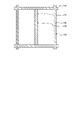
- FIG. 3 is a diagram illustrating a configuration example of a pixel according to the first embodiment of the present disclosure; This figure is a plan view showing a configuration example of the pixel 100 . This figure schematically shows the configuration of the pixel 100 viewed from the back surface side of the semiconductor substrate 120. As shown in FIG. A dotted-line rectangle in FIG. In addition, outline rectangles represent semiconductor regions and gate electrodes formed on the semiconductor substrate 120 . Semiconductor regions 121 and 122 forming photoelectric conversion units 101 and 102 are arranged in the pixel 100 , and charge transfer units 105 and 106 are arranged adjacent to the semiconductor regions 121 and 122 .
- gate electrodes 134 and 135 of charge transfer portions 105 and 106 are shown.
- Semiconductor regions 123 and 124 forming the charge holding portions 103 and 104 are arranged adjacent to the charge transfer portions 105 and 106 .
- Gate electrodes 134 and 135 and semiconductor regions 123 and 124 are arranged on the surface side of semiconductor substrate 120 .
- An overflow path 107 is arranged in the semiconductor substrate 120 between the pixel separation section 160 and the intra-pixel separation section 150, which will be described later.
- Pixel 100 in the figure represents an example in which two overflow paths 107a and 107b are arranged.
- Overflow paths 107a and 107b are formed by semiconductor regions 125 and 126, respectively.
- An intra-pixel separation unit 150 is arranged between the photoelectric conversion units 101 and 102 .
- the intra-pixel separation unit 150 separates the photoelectric conversion units 101 and 102 .
- An electrode 152 that constitutes the above-described intra-pixel isolation electrode 108 is arranged in the intra-pixel isolation portion 150 .
- a pixel separation section 160 is arranged at the boundary of the pixels 100 .
- the pixel separation section 160 is configured in a shape surrounding the pixel 100 and separates adjacent pixels 100 from each other.
- An electrode 162 that constitutes the pixel separation electrode 109 described above is arranged in the pixel separation section 160 .
- the image signal generation unit 110 is also shown in the figure.
- the figure shows an example in which the image signal generator 110 is arranged in a region other than the pixels 100 .
- a pixel 100 in the figure is connected to charge holding portions 103 and 104 by a signal line 119 .
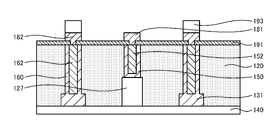
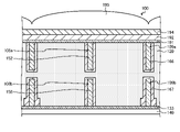
- FIG. 4 is a cross-sectional view showing a configuration example of a pixel according to the first embodiment of the present disclosure. This figure is a cross-sectional view showing a configuration example of the pixel 100 .
- the pixel 100 shown in FIG. a color filter 192 , a light shielding wall 193 , a planarizing film 194 and an on-chip lens 195 .
- the semiconductor substrate 120 is a semiconductor substrate on which the diffusion layers of the elements of the pixel 100 are arranged.
- the semiconductor substrate 120 can be made of silicon (Si), for example.
- Elements such as the photoelectric conversion unit 101 can be arranged in a well region formed in the semiconductor substrate 120 .
- the semiconductor substrate 120 in the figure is configured as a p-type well region. By arranging an n-type or p-type semiconductor region in this well region, a diffusion layer of the device can be formed.
- photoelectric conversion units 101 and 102, charge transfer units 105 and 106, charge holding units 103 and 104, and an overflow path 107 are shown.
- the photoelectric conversion unit 101 is composed of an n-type semiconductor region 121 .
- a photodiode with a pn junction at the interface between the n-type semiconductor region 121 and the surrounding p-type well region corresponds to the photoelectric conversion unit 101 .
- the photoelectric conversion unit 102 is composed of an n-type semiconductor region 122 .
- Charges generated by photoelectric conversion of the photoelectric conversion units 101 and 102 during the exposure period are accumulated in the n-type semiconductor regions 121 and 122, respectively.
- the accumulated charges are transferred to and held in the charge holding units 103 and 104 by the charge transfer units 105 and 106 after the exposure period has elapsed.
- Part of the semiconductor regions 121 and 122 in FIG. This extended region constitutes the source regions of charge transfer portions 105 and 106, which will be described later.
- n-type semiconductor regions 123 and 124 forming the charge holding portions 103 and 104 are arranged on the surface side of the semiconductor substrate 120 .
- These n-type semiconductor regions 123 and 124 are semiconductor regions with a relatively high impurity concentration, and constitute the FD described above.
- a semiconductor region 125 forming an overflow path 107 is arranged between the n-type semiconductor regions 121 and 122 forming the photoelectric conversion units 101 and 102, respectively.
- the semiconductor region 125 is configured to have the same conductivity type as the semiconductor regions 121 and 122 and is arranged adjacent to the semiconductor regions 121 and 122 .
- a potential barrier is formed between semiconductor region 125 and semiconductor regions 121 and 122 . By lowering this potential barrier, charges can be transferred between the semiconductor regions 121 and 122 .
- An intra-pixel separation unit 150 is arranged between the photoelectric conversion units 101 and 102 .
- the intra-pixel isolation portion 150 is made of an insulating member and electrically isolates the photoelectric conversion portions 101 and 102 .
- the intra-pixel isolation part 150 in the same figure represents an example arranged on the back side of the semiconductor substrate 120 , and insulating material such as silicon oxide (SiO 2 ) is provided in a groove part 151 formed from the back side of the semiconductor substrate 120 . It can be configured by embedding a member.
- the in-pixel isolation electrode 108 is arranged in the in-pixel isolation portion 150 .
- the in-pixel isolation electrode 108 can be formed by arranging an electrode 152 in the central portion of a groove 151 formed in the semiconductor substrate 120 .
- Electrode 152 can be made of, for example, tungsten.
- An intra-pixel isolation region 127 is arranged between the photoelectric conversion units 101 and 102 on the surface side of the semiconductor substrate 120 .
- This intra-pixel isolation region 127 prevents charge transfer between the photoelectric conversion units 101 and 102 .
- the in-pixel isolation region 127 can be composed of a semiconductor region having the same conductivity type as the well region and having a relatively high impurity concentration.
- a pixel separating portion 160 is arranged on the semiconductor substrate 120 at the boundary of the pixels 100 .
- the pixel separating section 160 is made of an insulating member and electrically separates the pixels 100 from each other.
- the pixel separation section 160 in the figure represents an example arranged on the back surface side of the semiconductor substrate 120 .
- the pixel separation section 160 in the figure can be configured by embedding an insulating member such as SiO 2 in a groove section 161 formed from the surface side of the semiconductor substrate 120 .
- a pixel separation electrode 109 is arranged in the pixel separation section 160 .
- This pixel separation electrode 109 can be formed by arranging an electrode 162 in the central portion of a groove 161 formed in the semiconductor substrate 120 .
- the electrode 162 can be made of tungsten, for example.
- a separation portion 131 is arranged on the front surface side of the semiconductor substrate 120 at the boundary of the pixels 100 .
- This isolation portion 131 can be formed by embedding an insulating member in a relatively shallow groove portion 132 formed on the surface side of the semiconductor substrate 120 .
- This separator 131 is called STI (Shallow Trench Isolation).
- the separation section 131 can be arranged at a position overlapping the pixel separation section 160 .
- the insulating film 133 is a film that insulates the surface side of the semiconductor substrate 120 .
- This insulating film 133 can be made of SiO 2 or silicon nitride (SiN).
- Gate electrodes 134 and 135 are arranged on the surface side of the semiconductor substrate 120 . Gate electrodes 134 and 135 constitute the gates of charge transfer sections 105 and 106, respectively. Gate electrodes 134 and 135 can be made of polycrystalline silicon.
- the insulating film 133 below the gate electrodes 134 and 135 forms a gate insulating film.
- the charge transfer unit 105 is composed of a MOS transistor having a semiconductor region 121 and a semiconductor region 123 as a source region and a drain region, respectively.
- the charge transfer section 106 is composed of a MOS transistor having a semiconductor region 122 and a semiconductor region 124 as a source region and a drain region, respectively.
- the wiring region 140 is arranged on the surface side of the semiconductor substrate 120 and is a region in which the wiring of the pixels 100 is arranged.
- This wiring region 140 includes wiring 142 and an insulating layer 141 .
- the wiring 142 transmits signals and the like of the elements of the pixel 100 .
- This wiring 142 can be made of a conductor such as copper (Cu) or tungsten.
- the insulating layer 141 insulates the wiring 142 and the like.
- This insulating layer 141 can be made of, for example, SiO 2 .
- a contact plug 143 is arranged between the semiconductor region of the semiconductor substrate 120 or the gate electrode 134 and the wiring 142 .
- This contact plug 143 can be made of a columnar metal.
- the insulating film 191 insulates the back side of the semiconductor substrate 120 .
- This insulating film 191 can be made of, for example, SiO 2 .
- the in-pixel isolation wiring 181 and the pixel isolation wiring 182 are wirings arranged on the back side of the semiconductor substrate 120 and connected to the in-pixel isolation electrode 108 and the pixel isolation electrode 109 .
- the in-pixel isolation wiring 181 is connected to the in-pixel isolation electrode 108
- the pixel isolation wiring 182 is connected to the pixel isolation electrode 109 .
- the in-pixel isolation wiring 181 and the pixel isolation wiring 182 are connected to the in-pixel isolation electrode 108 and the pixel isolation electrode 109 through an opening 189 formed in the insulating film 191 .
- the intra-pixel isolation wiring 181 and the pixel isolation wiring 182 can be made of metal such as tungsten.
- the color filter 192 is an optical filter that transmits light of a predetermined wavelength among incident light.
- a color filter that transmits red light, green light and blue light can be used.
- the light shielding wall 193 is arranged in the region of the color filter 192 on the boundary of the pixels 100 to shield the incident light from the adjacent pixels 100 .
- the planarization film 194 is a film that planarizes the surface of the color filter 192 .
- the on-chip lens 195 is a lens that collects incident light.
- This on-chip lens 195 is configured in a hemispherical shape and converges incident light onto the photoelectric conversion units 101 and 102 .
- the pixel 100 in the same figure performs imaging with incident light irradiated to the back side of the semiconductor substrate 120 .
- the imaging device 1 including such pixels 100 is called a back-illuminated imaging device.
- the in-pixel separation section 150 and the pixel separation section 160 are embedded in the semiconductor substrate 120 .
- an interface state is formed as described above, which causes dark current. Therefore, a charge accumulation region in which holes are accumulated is formed near the interface of the semiconductor substrate 120 to reduce the effect of dark current.
- This charge accumulation region can be formed by applying a negative bias voltage to the intra-pixel isolation electrode 108 and the pixel isolation electrode 109 . By increasing the absolute value of this bias voltage, the width of the charge storage region can be increased. The influence of interface states can be further reduced.
- the absolute value of the bias voltage is increased to increase the charge accumulation region, the saturated charge amounts of the photoelectric conversion units 101 and 102 are reduced. This is because the semiconductor region capable of storing charges is reduced. Since the pixel separation section 160 is configured in a shape surrounding the pixel 100, the influence of the change in the bias voltage of the pixel separation electrode 109 on the saturation charge amount is increased.
- the bias voltage of the pixel separation electrode 109 can be, for example, a voltage corresponding to the bandgap of Si forming the semiconductor substrate 120, eg, -1.4V.
- the bias voltage applied to the pixel separation electrode 109 is adjusted according to the desired charge storage capacity (saturated charge amount described later) for the photoelectric conversion units 101 and 102 and the thickness of the insulating member forming the pixel separation unit 160.
- a voltage different from the voltage corresponding to the bandgap of Si eg, ⁇ 1.2 V, can also be used.
- the absolute value of the bias voltage can be lowered after the charge accumulation region is formed in the pixel separation section 160 or the like.
- the bias voltage of the intra-pixel separation electrode 108 can be the same voltage as the bias voltage of the pixel separation electrode 109 . Also, the bias voltage of the intra-pixel separation electrode 108 can be set to a voltage different from the bias voltage of the pixel separation electrode 109 .
- the bias voltages of the pixel separation electrode 109 and the in-pixel separation electrode 108 are hereinafter referred to as a first bias voltage and a second bias voltage, respectively.
- the photoelectric conversion units 101 and 102 perform photoelectric conversion during the exposure period to generate charges and store them in their own semiconductor regions 121 and 122, respectively.
- the charge amount that can be stored in the semiconductor region 121 or the like is called a saturated charge amount. Charges generated exceeding this saturated charge amount overflow the semiconductor regions 121 and 122 and move to the charge holding portions 103 and 104 . The charges that have moved to the charge holding portions 103 and 104 are discharged by resetting.
- the charge amounts accumulated in the semiconductor regions 121 and 122 are also different values. For example, if the on-chip lens 195 is displaced toward the photoelectric conversion unit 101 due to variations in the manufacturing process, a large amount of charge is generated and accumulated in the photoelectric conversion unit 101 . When the accumulated charge amount reaches the saturation charge amount during the exposure period, charge overflow occurs in the photoelectric conversion unit 101 . On the other hand, the photoelectric conversion unit 102 continues to accumulate charges because the accumulated charge amount has not reached the saturated charge amount. This situation poses a problem in the image signal mode in which the batch transfer is performed as described above.
- the overflow path 107 is arranged to move the charge to the photoelectric conversion unit 102 before the accumulated charge amount of the photoelectric conversion unit 101 reaches the saturated charge amount. Thereby, the linearity of the image signal can be maintained.
- a negative second bias voltage to the intra-pixel separation electrode 108, the potential barrier of the overflow path 107 can be adjusted. For example, by applying a second bias voltage of ⁇ 0.5 V to the intra-pixel separation electrode 108, the potential barrier of the overflow path 107 can be lowered. Charges can be transferred between the photoelectric conversion units 101 and 102 .
- the potential barrier of the overflow path 107 is raised to limit the charge transfer between the photoelectric conversion units 101 and 102 .
- This increases the saturation charge amount of the photoelectric conversion units 101 and 102 .
- the amplitude of the phase difference signal can be increased, and the detection range of the image plane phase difference can be widened.
- the second bias voltage in the phase difference signal mode can be -2V, for example.
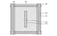
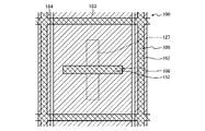
- FIGS. 5A to 5C are diagrams showing configuration examples of back-side wiring according to the first embodiment of the present disclosure. This figure is a diagram showing a configuration example of the intra-pixel isolation wiring 181 and the pixel isolation wiring 182 .
- FIG. 5A is a diagram showing an example in which the in-pixel isolation wiring 181 and the pixel isolation wiring 182 are arranged in the same direction as the in-pixel isolation electrode 108 .
- FIG. 5B is a diagram showing an example in which the in-pixel isolation wiring 181 and the pixel isolation wiring 182 are arranged in a direction different from that of the in-pixel isolation electrode 108 .
- FIG. 5C is a diagram showing a cross-sectional configuration of the intra-pixel isolation wiring 181 and the pixel isolation wiring 182 at the boundary of the pixel 100.
- FIG. A light shielding wall 193 is arranged on the boundary of the pixel 100 .
- the light shielding wall 193 is formed in a shape that covers the intra-pixel isolation wiring 181 and the pixel isolation wiring 182 . Further, the thickness of the light shielding wall 193 is adjusted depending on whether or not the intra-pixel isolation wiring 181 and the pixel isolation wiring 182 are arranged. Thereby, the surface of the light shielding wall 193 can be flattened.
- intra-pixel isolation wiring 181 and the pixel isolation wiring 182 shown in FIG. This through via can be arranged in a region outside the pixel region 3 described in FIG.
- FIG. 6 is a diagram illustrating an example of generation of an image signal and a phase difference signal according to an embodiment of the present disclosure; This figure is a timing chart showing an example of generation of an image signal and a phase difference signal in the pixel 100. As shown in FIG.
- RST, SEL, TRG1” and “TRG2” in the figure represent signals of the signal line RST, the signal line SEL, the signal line TRG1 and the signal line TRG2, respectively. These represent the waveforms of the binarized control signals, and the portion of the value "1" represents the region to which the ON signal is transmitted.
- Vb1 represents the first bias voltage transmitted by the signal line Vb1.
- Vb2 represents the second bias voltage transmitted by the signal line Vb2.
- the dashed line represents the level of 0V.
- VO represents the output of the signal line VO.
- the first half of the figure represents the procedure for the phase difference signal mode, and the latter half represents the procedure for the image signal mode.
- the value "0" is applied to the signal line RST, signal line SEL, signal line TRG1 and signal line TRG2.
- a bias voltage of -2V is applied to the signal line Vb2.
- a bias voltage of ⁇ 1.2 V is applied to the signal line Vb1 during the entire period of the phase difference signal mode.
- an ON signal is applied to the signal lines RST, TRG1 and TRG2.
- the reset transistor 111 and the charge transfer units 105 and 106 become conductive, and the photoelectric conversion units 101 and 102 and the charge holding units 103 and 104 are reset.
- a bias voltage of 0V is applied to the signal line Vb2.
- the potential barrier of overflow path 107 is lowered and the charge is drained.
- the application of ON signals to the signal lines RST, TRG1 and TRG2 is stopped.
- an exposure period is started, and charges generated by photoelectric conversion are accumulated in the photoelectric conversion units 101 and 102 .
- the bias voltage of the signal line Vb2 returns to -2V.
- an ON signal is applied to the signal line SEL.
- the application of the ON signal to the signal line SEL continues until the phase difference signals of the pixels 100 for one row of the pixel section 3 are output.
- an ON signal is applied to the signal line TRG1.
- the charge transfer unit 105 becomes conductive, and the charges accumulated in the photoelectric conversion unit 101 are transferred to the charge holding units 103 and 104 .
- an ON signal is applied to the signal line RST, and the charge holding units 103 and 104 are reset.
- a bias voltage of 0V is applied to the signal line Vb2.
- an ON signal is applied to the signal line TRG2.
- the charge transfer unit 106 becomes conductive, and the charges accumulated in the photoelectric conversion unit 102 are transferred to the charge holding units 103 and 104 .
- phase difference signals can be generated in the phase difference signal mode.
- image signal mode will be explained.
- the value "0" is applied to the signal line RST, signal line SEL, signal line TRG1 and signal line TRG2.
- a bias voltage of -0.3V is applied to the signal line Vb2.
- a bias voltage of -1.4 V is applied to the signal line Vb1 during the entire period of the image signal mode.
- an ON signal is applied to the signal lines RST, TRG1 and TRG2.
- the reset transistor 111 and the charge transfer units 105 and 106 become conductive, and the photoelectric conversion units 101 and 102 and the charge holding units 103 and 104 are reset.
- a bias voltage of 0V is applied to the signal line Vb2.
- the application of the ON signal to the signal lines RST, TRG1 and TRG2 is stopped. Also, the bias voltage of the signal line Vb2 returns to -0.3V. As a result, an exposure period is started, and charges generated by photoelectric conversion are accumulated in the photoelectric conversion units 101 and 102 .
- an ON signal is applied to the signal line SEL.
- the application of the ON signal to the signal line SEL continues until the image signals of the pixels 100 for one row of the pixel section 3 are output.
- an ON signal is applied to the signal line RST, and the charge holding units 103 and 104 are reset.
- a bias voltage of 0V is applied to the signal line Vb2.
- the exposure period ends.
- an ON signal is applied to the signal lines TRG1 and TRG2.
- the charge transfer units 105 and 106 become conductive, and charges accumulated in the photoelectric conversion units 101 and 102 are transferred to the charge holding units 103 and 104 .
- the phase difference signal and the image signal can be generated.
- the bias voltages of the signal lines Vb1 and Vb2 are described as examples, and other bias voltages can be applied.
- FIGS. 7A-7S are diagrams illustrating an example of a method for manufacturing an imaging device according to the first embodiment of the present disclosure. These figures are diagrams showing an example of the manufacturing process of the imaging device 1 .
- a well region is formed in a semiconductor substrate 120, and a semiconductor region 121 (not shown) and the like are formed (FIG. 7A).
- a groove portion 132 is formed in a region on the surface side of the semiconductor substrate 120 where the separation portion 131 is to be arranged. This can be done by dry etching.
- an insulating film 509 is placed in the trench 132 (FIG. 7B). This can be done by embedding an insulating member such as SiO 2 in the trench 132 using CVD (Chemical Vapor Deposition) or the like and planarizing the surface.
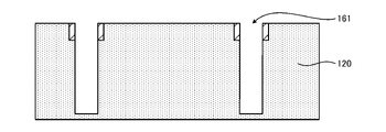
- a groove portion 161 is formed in a region where the pixel separation portion 160 is arranged on the surface side of the semiconductor substrate 120 (FIG. 7C). This can be done by dry etching.
- an insulating member is placed on the wall surface of the groove 161 to form the pixel separation section 160 (FIG. 7D). This can be done by depositing a film such as SiO 2 using CVD or the like.
- the pixel separation electrode 109 is formed by arranging the electrode 162 in the groove 161 (FIG. 7E). This can be done by forming a film of tungsten or the like using CVD or the like.
- an insulating member is placed in the opening 501 to form the separating portion 131 (FIG. 7G). This can be done by depositing a film such as SiO 2 using CVD or the like.
- an in-pixel isolation region 127 is formed on the surface side of the semiconductor substrate 120 (FIG. 7H). This can be done by ion implantation.
- an insulating film 133 (not shown) and gate electrodes 134 and 135 (not shown) are formed on the surface side of the semiconductor substrate 120 .
- a wiring region 140 is formed (FIG. 7I).
- the semiconductor substrate 120 is turned upside down and the back side is ground to make it thinner. Grinding of the semiconductor substrate 120 can be performed by CMP (Chemical Mechanical Polishing). As a result, the pixel separation portion 160 and the pixel separation electrode 109 are exposed on the back surface side of the semiconductor substrate 120 (FIG. 7J).
- a groove portion 151 is formed in a region where the in-pixel isolation portion 150 is arranged on the back side of the semiconductor substrate 120 (FIG. 7K). This can be done by dry etching.
- an insulating member is placed on the wall surface of the groove portion 151 to form the intra-pixel separation portion 150 (FIG. 7L). This can be done by depositing a film such as SiO 2 using CVD or the like.
- an electrode 152 is placed in the groove 151 to form the intra-pixel isolation electrode 108 (FIG. 7M). This can be done by forming a film of tungsten or the like using CVD or the like.
- an insulating film 191 is arranged on the back surface side of the semiconductor substrate 120 (FIG. 7N). This can be done by depositing a film such as SiO 2 using CVD or the like.
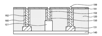
- an opening 199 is formed in the insulating film 191 adjacent to the in-pixel isolation electrode 108 and the pixel isolation electrode 109 (FIG. 7O).
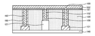
- a material film 502 such as the intra-pixel isolation wiring 181 is arranged on the back side of the semiconductor substrate 120 including the opening 199 (FIG. 7P). This can be done by depositing a film of tungsten using CVD or the like.
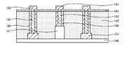
- the material film 502 is etched to form the intra-pixel isolation wiring 181 and the pixel isolation wiring 182 (FIG. 7Q).
- a light shielding wall 193 is arranged on the boundary of the pixels 100 on the back side of the semiconductor substrate 120 (Fig. 7R).
- a color filter 192 is formed on the back side of the semiconductor substrate 120 (Fig. 7S). After that, a planarizing film 194 and an on-chip lens 195 are arranged.
- the imaging device 1 can be manufactured through the above steps.
- the imaging device 1 can separate the photoelectric conversion units 101 and 102 arranged in the pixel 100 by arranging the intra-pixel separation unit 150 in the pixel 100 .
- the in-pixel isolation electrode 108 By disposing the in-pixel isolation electrode 108 in the in-pixel isolation portion 150 and applying a bias voltage, a charge accumulation region can be formed and dark current can be reduced.
- the pixel separating section 160 is arranged at the boundary between the pixels 100 .
- the imaging element 1 of the second embodiment of the present disclosure differs from the above-described first embodiment in that the pixel separation section 160 having a shape penetrating the semiconductor substrate 120 of the pixel 100 is arranged.
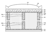
- FIG. 8 is a cross-sectional view showing a configuration example of a pixel according to the second embodiment of the present disclosure. Similar to FIG. 4, this figure is a cross-sectional view showing a configuration example of the pixel 100. As shown in FIG. The pixel 100 shown in FIG. 4 is different from the pixel 100 shown in FIG.
- the configuration of the imaging device 1 other than this is the same as the configuration of the imaging device 1 in the first embodiment of the present disclosure, the description is omitted.
- the imaging device 1 of the second embodiment of the present disclosure includes the pixel separation section 160 and the pixel separation electrode 109 having a shape penetrating the semiconductor substrate 120 .
- the charge accumulation region at the boundary of the pixel 100 can be widened, and the dark current can be further reduced.
- the wiring of the pixel separation electrode 109 is arranged on the back side of the semiconductor substrate 120 .
- the imaging element 1 of the third embodiment of the present disclosure differs from the above-described second embodiment in that the wiring of the pixel separation electrode 109 is arranged on the surface side of the semiconductor substrate 120 .
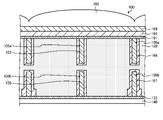
- FIG. 9 is a cross-sectional view showing a configuration example of a pixel according to the third embodiment of the present disclosure. Similar to FIG. 8, this figure is a cross-sectional view showing a configuration example of the pixel 100. As shown in FIG. The pixel 100 in FIG. 8 differs from the pixel 100 in FIG. 8 in that the contact plug 143 and the wiring 142 are connected to the pixel separation electrode 109 instead of the pixel separation wiring 182 .
- the pixel separation electrode 109 is formed in a shape penetrating the semiconductor substrate 120 . Therefore, an opening can be formed in the insulating film 133 adjacent to the pixel separation electrode 109 to arrange the contact plug 143 and connect it to the wiring 142 .
- a first bias voltage is applied to the pixel separation electrode 109 in the figure through the wiring 142 in the wiring region 140 .
- the pixel separation wiring 182 can be omitted from the pixel 100 in FIG.
- the configuration of the imaging device 1 other than this is the same as the configuration of the imaging device 1 according to the second embodiment of the present disclosure, so the description is omitted.
- the imaging device 1 of the third embodiment of the present disclosure applies the first bias voltage to the pixel separation electrodes 109 using the contact plugs 143 and the wirings 142 in the wiring regions 140 .
- the pixel isolation wiring 182 can be omitted, and the configuration of the pixel 100 can be simplified.
- the image sensor 1 of the first embodiment described above uses the intra-pixel isolation wiring 181 and the pixel isolation wiring 182 made of metal such as tungsten.
- the imaging element 1 of the fourth embodiment of the present disclosure differs from the above-described first embodiment in that it uses rear-side wiring formed of a transparent member.
- FIGS. 10A and 10B are diagrams showing configuration examples of back-side wiring according to the fourth embodiment of the present disclosure.
- This figure like FIGS. 5A and 5B, is a plan view showing a configuration example of the backside wiring.
- the pixel 100 in FIG. 5 differs from FIGS. 5A and 5B in that an intra-pixel isolation wiring 183 and a pixel isolation wiring 184 are provided instead of the intra-pixel isolation wiring 181 and the pixel isolation wiring 182 .
- the intra-pixel separation wiring 183 and the pixel separation wiring 184 are wirings made of a transparent member such as a transparent conductive film.
- the in-pixel isolation wiring 183 is connected to the in-pixel isolation electrode 108
- the pixel isolation wiring 184 is connected to the pixel isolation electrode 109 .
- the intra-pixel isolation wiring 183 and the pixel isolation wiring 184 are made of, for example, ITO (Indium Tin Oxide), In 2 O 3 , ZnO (Zinc Oxide), IZO (Indium Zinc Oxide), and IGZO (In-Ga-Zn-O). ).
- FIG. 10A shows an example in which the in-pixel isolation wiring 183 and the pixel isolation wiring 184 are arranged in the same direction as the in-pixel isolation electrode 108
- FIG. 10B shows an example in which the in-pixel isolation wiring 183 and the pixel isolation wiring 184 It shows an example in which it is arranged in a direction different from that of the in-pixel separation electrode 108 .
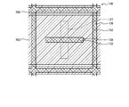
- FIGS. 10A and 10B are diagrams showing other configuration examples of back-side wiring according to the fourth embodiment of the present disclosure.
- This figure like FIGS. 10A and 10B, is a plan view showing a configuration example of the backside wiring.
- the intra-pixel isolation wiring 183 in FIG. 10 differs from the intra-pixel isolation wiring 183 in FIGS.
- the intra-pixel isolation wiring 183 in FIG. A transparent conductive film generally has a lower conductivity than a metal film. Therefore, the in-pixel isolation wiring 183 has a higher resistance value than the in-pixel isolation wiring 181 formed of a metal film. As shown in FIG. 6, the second bias voltage frequently changes. When the resistance value of the intra-pixel isolation wiring 183 that transmits the second bias voltage is high, the delay time increases and the second bias voltage for each pixel 100 differs. As a result, unevenness occurs in the image signal.
- the intra-pixel isolation wiring 183 is configured to be wide. As a result, the resistance of the intra-pixel isolation wiring 183 can be reduced, and the delay time of transmission of the second bias voltage can be shortened.
- [Modification] 11C and 11D are diagrams showing modifications of the configuration of the pixel 100 according to the fourth embodiment of the present disclosure.
- the intra-pixel isolation electrode 108 in the figure is arranged in a direction different from that of the intra-pixel isolation region 127 and represents an example in which it is arranged in a direction perpendicular to the boundary between the photoelectric conversion units 101 and 102 .
- Incident light can be reflected to a region such as the photoelectric conversion portion 101 by the in-pixel separation electrode 108 .
- the conversion efficiency of the pixel 100 can be improved.
- the configuration of the imaging device 1 other than this is the same as the configuration of the imaging device 1 in the first embodiment of the present disclosure, the description is omitted.
- the imaging element 1 of the fourth embodiment of the present disclosure includes the intra-pixel isolation wiring 183 and the pixel isolation wiring 184 that are made of a transparent member in the pixel 100 .
- the amount of incident light to the photoelectric conversion unit 101 can be increased.
- the sensitivity of the pixel 100 can be improved.
- the imaging device 1 of the first embodiment described above includes the in-pixel separation section 150 and the pixel separation section 160 arranged on the back side of the semiconductor substrate 120 .
- the imaging device 1 of the fifth embodiment of the present disclosure differs from the above-described first embodiment in that it includes an intra-pixel separation section and a pixel separation section on both surfaces of the semiconductor substrate 120 .
- FIG. 12 is a cross-sectional view showing a configuration example of a pixel according to the fifth embodiment of the present disclosure. Similar to FIG. 4, this figure is a cross-sectional view showing a configuration example of the pixel 100. As shown in FIG. The pixel 100 in FIG. 4 differs from the pixel 100 in FIG. 4 in that an intra-pixel isolation portion 154 is arranged instead of the intra-pixel isolation region 127 and a pixel isolation portion 164 is further arranged.
- the in-pixel isolation portion 154 is an in-pixel isolation portion arranged on the surface side of the semiconductor substrate 120 .
- the in-pixel isolation portion 154 can be formed by embedding an insulating member in a groove portion 155 formed from the surface side of the semiconductor substrate 120 .
- an in-pixel isolation electrode 108 can be further arranged in the in-pixel isolation portion 154 .
- the in-pixel isolation electrodes 108 arranged in the in-pixel isolation portion 150 and the in-pixel isolation portion 154 are distinguished by adding symbols “a” and “b”.
- the intra-pixel separation electrode 108 b can be configured by an electrode 156 arranged in the central portion of the groove portion 155 .
- the pixel separation section 160 in the same drawing is arranged on the front surface side of the semiconductor substrate 120 .
- a pixel separating portion 164 is arranged at the boundary of the pixels 100 on the back side of the semiconductor substrate 120 .
- the pixel separating portion 164 can be formed by embedding an insulating member in a groove portion 165 formed from the back side of the semiconductor substrate 120 .
- the pixel separation electrode 109 can be further arranged in the pixel separation portion 164 .
- the pixel separation electrodes 109 arranged in the pixel separation section 160 and the pixel separation section 164 are distinguished by adding symbols “a” and “b”.
- the pixel separation electrode 109 b can be composed of an electrode 166 arranged in the central portion of the groove portion 165 .
- the pixel 100 in the same figure has overflow paths 107a and 107b.
- the overflow path 107 a is an overflow path configured by the semiconductor region 125 arranged between the in-pixel isolation portion 150 and the pixel isolation portion 164 .
- the overflow path 107 b is an overflow path configured by the semiconductor region 128 arranged between the in-pixel isolation portions 150 and 154 . Note that either one of the overflow paths 107a and 107b can be arranged.
- the same second bias voltage as that applied to the in-pixel separated electrode 108a can be applied to the in-pixel separated electrode 108b. Also, a second bias voltage different from the in-pixel isolation electrode 108a can be applied to the in-pixel isolation electrode 108b.
- a pixel separation portion wiring 184 is connected to the pixel separation electrode 109a.
- the contact plug 143 and the wiring 142 of the wiring region 140 can be connected to the pixel separation electrode 109b.
- the same first bias voltage as the pixel separation electrode 109a can be applied to the pixel separation electrode 109b.
- a first bias voltage different from that applied to the pixel separation electrode 109a can be applied to the pixel separation electrode 109b.
- the pixel 100 in FIG. 1 includes intra-pixel separation electrodes 108 a and 108 b and pixel separation electrodes 109 a and 109 b on both sides of a semiconductor substrate 120 .
- the saturation charge amount and the dark current of the photoelectric conversion units 101 and 102 can be adjusted on both surfaces of the semiconductor substrate 120 respectively.
- the intra-pixel separating section 154 is an example of the second intra-pixel separating section described in the claims.
- the in-pixel separation electrode 108b is an example of the second in-pixel separation electrode described in the claims.
- the pixel separating section 160 in the figure is an example of the second pixel separating section described in the claims.
- the pixel separation electrode 109b in the figure is an example of the second pixel separation electrode described in the claims.
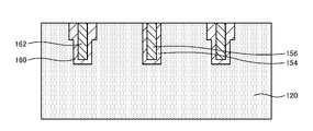
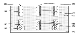
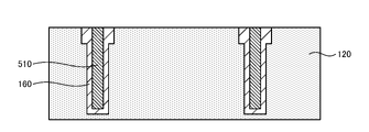
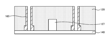
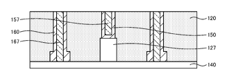
- FIGS. 13A-13E are diagrams illustrating an example of a method for manufacturing an imaging device according to the fifth embodiment of the present disclosure. This figure is a diagram showing an example of the manufacturing process of the intra-pixel separating sections 150 and 154 and the pixel separating sections 160 and 164 in the manufacturing process of the imaging device 1 according to the fifth embodiment of the present disclosure.
- grooves 161 and 155 are formed on the surface side of the semiconductor substrate 120 .
- an insulating member is placed on the wall surfaces of the grooves 161 and 155 to form the intra-pixel separation section 154 and the pixel separation section 160 .
- electrodes 156 and 162 are formed by placing a conductive member in grooves 161 and 155 (FIG. 13A).
- a wiring region 140 is formed on the surface side of the semiconductor substrate 120 .
- the semiconductor substrate 120 is turned upside down, and the back side of the semiconductor substrate 120 is ground (FIG. 13B).
- grooves 151 and 165 are formed on the back side of the semiconductor substrate 120 (FIG. 13C).
- an insulating member is placed on the walls of the grooves 151 and 165 to form the intra-pixel separation section 150 and the pixel separation section 164 (FIG. 13D).
- electrodes 156 and 162 are formed by arranging conductive members in the grooves 151 and 165 (FIG. 13E).
- the configuration of the imaging device 1 other than this is the same as the configuration of the imaging device 1 in the first embodiment of the present disclosure, the description is omitted.
- the imaging device 1 of the fifth embodiment of the present disclosure includes the intra-pixel separation electrodes 108a and 108b and the pixel separation electrodes 109a and 109b on both sides of the semiconductor substrate 120. It becomes possible to adjust the bias voltages applied to these, respectively, and the bias voltages to be applied can be optimized.
- the image pickup device 1 of the first embodiment described above uses the intra-pixel separation electrode 108 and the pixel separation electrode 109 configured by the metal electrodes 152 and 162 .
- the imaging device 1 of the sixth embodiment of the present disclosure uses the in-pixel separation electrode 108 and the pixel separation electrode 109 configured by electrodes of a transparent conductive film, which is different from that of the above-described first embodiment. different from
- FIG. 14 is a cross-sectional view showing a configuration example of a pixel according to the sixth embodiment of the present disclosure. Similar to FIG. 4, this figure is a cross-sectional view showing a configuration example of the pixel 100. As shown in FIG. The pixel 100 in FIG. 4 differs from the pixel 100 in FIG. 4 in that an electrode 157 is arranged instead of the electrode 152 and an electrode 167 is arranged instead of the electrode 162 .
- the intra-pixel separation electrode 108 in the figure is composed of an electrode 157 .
- the pixel separation electrode 109 in FIG. These electrodes 157 and 167 are composed of a transparent member such as a transparent conductive film. The member described in FIG. 10A can be applied to this transparent conductive film.
- the configuration of the imaging device 1 is not limited to this example.
- the in-pixel isolation wiring 181 and the pixel isolation wiring 182 instead of the in-pixel isolation wiring 183 and the pixel isolation wiring 184 described with reference to FIG. 10A can be arranged.
- FIGS. 15A-15D are diagrams illustrating an example of a method for manufacturing an imaging device according to the sixth embodiment of the present disclosure. This figure is a diagram showing an example of the manufacturing process of the intra-pixel separating section 150 and the pixel separating section 160 in the manufacturing process of the imaging device 1 according to the sixth embodiment of the present disclosure.
- grooves 161 are formed on the surface side of the semiconductor substrate 120 .
- an insulating member is placed on the wall surface of the groove 161 to form the pixel separation section 160 (FIG. 15A).
- a transparent conductive film is arranged in the groove 161 to form an electrode 167 (FIG. 15B).
- an in-pixel isolation region 127 is formed on the semiconductor substrate 120 and a wiring region 140 is formed on the surface side of the semiconductor substrate 120 .
- the semiconductor substrate 120 is turned upside down, and the back side of the semiconductor substrate 120 is ground.
- a groove portion 151 is formed on the back surface side of the semiconductor substrate 120 (FIG. 15C).
- an insulating member is arranged on the wall surface of the groove portion 151 to form the intra-pixel isolation portion 150 .
- a transparent conductive film is placed in the groove 151 to form an electrode 157 (FIG. 15D).
- the electrodes 167 of the transparent conductive film are arranged in the grooves 151 formed on the surface side of the semiconductor substrate 120 . Therefore, it is necessary to apply a low-temperature process to subsequent steps. This is because the transparent conductive film has low heat resistance.
- FIGS. 16A-16H are diagrams showing another example of the method for manufacturing the imaging device according to the sixth embodiment of the present disclosure. This figure is a diagram showing another example of the manufacturing process of the intra-pixel separating section 150 and the pixel separating section 160 in the manufacturing process of the imaging device 1 according to the sixth embodiment of the present disclosure.
- grooves 161 are formed on the surface side of the semiconductor substrate 120 .
- an insulating member is arranged on the wall surface of the groove portion 161 to form the pixel separating portion 160 .
- the temporary electrode 510 is arranged in the groove portion 161 .
- This temporary electrode 510 can be made of, for example, polycrystalline silicon (FIG. 16A).
- an intra-pixel isolation region 127 is formed in the semiconductor substrate 120, and a wiring region 140 is formed on the surface side of the semiconductor substrate 120.
- the semiconductor substrate 120 is turned upside down, and the back side of the semiconductor substrate 120 is ground. (Fig. 16B).
- grooves 151 are formed on the back side of the semiconductor substrate 120 (FIG. 16E).
- an insulating member is arranged on the wall surface of the groove portion 151 to form the intra-pixel separation portion 150 (FIG. 16F).
- electrodes 157 and 167 are formed by placing a transparent conductive film in the grooves 151 and 161 (FIG. 16H).
- temporary electrodes 510 are arranged in grooves 161 formed on the surface side of the semiconductor substrate 120, as shown in FIG. 16A.
- This temporary electrode 510 is made of polycrystalline silicon.
- This polycrystalline silicon is a member having high heat resistance. Therefore, a high-temperature process, for example, a process of forming an insulating film by thermal oxidation of the semiconductor substrate 120 can be applied to subsequent steps.
- the imaging element 1 described in FIG. 12 uses the electrodes 152 and 156 and the electrodes 162 and 166 made of metal, electrodes made of a transparent conductive film can also be used.
- FIG. 17 is a cross-sectional view showing a configuration example of a pixel according to the first modification of the sixth embodiment of the present disclosure.
- This figure is a diagram showing a configuration example of the pixel 100, similar to FIG.
- the pixel 100 of FIG. 12 differs from the pixel 100 of FIG. 12 in that electrodes 157 and 158 are arranged instead of the electrodes 152 and 156 and electrodes 167 and 168 are arranged instead of the electrodes 162 and 166 .
- Electrodes 157 and 158 and electrodes 167 and 168 are electrodes made of a transparent conductive film.
- the imaging device 1 described with reference to FIG. 17 uses transparent conductive film electrodes for the electrodes 157 and 158 and the electrodes 167 and 168, but only some of the electrodes may be formed from the transparent conductive film.
- FIG. 18A and 18B are cross-sectional views showing configuration examples of pixels according to the second modification of the sixth embodiment of the present disclosure.
- This figure is a diagram showing a simplified configuration example of the pixel 100 .
- a pixel 100 in FIG. 18A is a diagram showing an example in which electrodes 157 and 168 made of a transparent conductive film are arranged on the back side of a semiconductor substrate 120 .
- FIG. 18B is a diagram showing an example in which electrodes 158 and 167 made of a transparent conductive film are arranged on the surface side of the semiconductor substrate 120. As shown in FIG.
- FIGS. 18A and 18B are cross-sectional views showing other configuration examples of pixels according to the second modification of the sixth embodiment of the present disclosure.
- This figure like FIGS. 18A and 18B, is a diagram showing a simplified configuration example of the pixel 100.
- FIG. A pixel 100 in FIG. 19A represents an example in which electrodes 157 and 158 made of a transparent conductive film are arranged on intra-pixel separation electrodes 108a and 108b.
- FIG. 19B is a diagram showing an example in which electrodes 167 and 168 made of a transparent conductive film are arranged on the pixel separation electrodes 109a and 109b.
- the configuration of the imaging device 1 other than this is the same as the configuration of the imaging device 1 in the first embodiment of the present disclosure, the description is omitted.
- the imaging device 1 of the sixth embodiment of the present disclosure applies a bias voltage to the intra-pixel separated electrode 108 and the pixel separated electrode 109 which are made of a transparent member.
- the image sensor 1 of the first embodiment described above uses the in-pixel separation electrode 108 and the pixel separation electrode 109, but it is also possible to use the in-pixel separation electrode 108 and the pixel separation electrode 109 having different shapes. can.
- FIGS. 20A-20C are diagrams showing configuration examples of pixels according to modifications of the present disclosure. This figure is a diagram showing a configuration example of the in-pixel separation electrode 108 and the pixel separation electrode 109 in the pixel 100 .
- FIG. 20A is a diagram showing the intra-pixel separation electrode 108 constituted by the electrode 152 divided into two in plan view of the semiconductor substrate 120.
- FIG. An overflow path 107 can be placed between the two electrodes 152 .
- the in-pixel separation electrode 108 and the pixel separation electrode 109 can be arranged so as to pass through the semiconductor substrate 120 .
- FIG. 20B is a diagram showing the intra-pixel separated electrode 108 constituted by the electrode 152 divided into two or more in plan view of the semiconductor substrate 120.
- An overflow path 107 can be positioned between the plurality of electrodes 152 .
- the overflow path 107 can be arranged between the electrode 152 and the electrode 152 forming the pixel separation electrode 109 .
- the in-pixel separation electrode 108 and the pixel separation electrode 109 can be arranged so as to pass through the semiconductor substrate 120 .
- FIG. 20C is a diagram showing the in-pixel separation electrode 108 formed by the electrode 152 having a shape that contacts the electrode 162 that forms the pixel separation electrode 109 in plan view of the semiconductor substrate 120 .
- the pixel separation electrode 109 having a shape penetrating the semiconductor substrate 120 and the pixel separation electrode 109 divided on the front side and the back side of the semiconductor substrate 120 can be arranged.
- the intra-pixel separation electrode 108 is arranged on the front surface side and the back surface side of the semiconductor substrate 120 .
- the overflow path 107 is arranged between the in-pixel separation electrodes 108 divided into the front side and the back side.
- FIGS. 21A and 22B are diagrams showing other configuration examples of pixels according to the modification of the present disclosure. This figure is a diagram showing a configuration example of the pixel separation electrode 109 in the pixel 100 .
- FIG. 21A is a diagram showing an example of the pixel separation electrode 109 constituted by an octagonal electrode 162 in plan view of the semiconductor substrate 120.
- FIG. 162 By forming the electrode 162 into an octagonal shape, it is possible to reduce the electric field concentration at the corner of the pixel 100 when the first bias voltage is applied to the electrode 162 .
- a through via 171 can be arranged at the corner of the pixel 100 .
- the through via 171 is a via plug shaped to penetrate the semiconductor substrate 120 and is a via plug connected to the wiring 142 in the wiring region 140 .
- FIG. 21B is a diagram showing an example of the pixel separation electrode 109 constituted by the electrode 162 with rounded corners in plan view of the semiconductor substrate 120 . Similar to electrode 162 in FIG. 21A, electric field concentration at the corners of pixel 100 when the first via voltage is applied can be reduced.
- the configuration of the imaging device 1 other than this is the same as the configuration of the imaging device 1 in the first embodiment of the present disclosure, the description is omitted.
- the imaging device 1 as described above can be applied to various electronic devices such as imaging systems such as digital still cameras and digital video cameras, mobile phones with imaging functions, and other devices with imaging functions. can be done.
- FIG. 22 is a block diagram showing a configuration example of an imaging device mounted on an electronic device.
- an imaging device 701 includes an optical system 702, an imaging element 703, and a DSP (Digital Signal Processor) 704. , a recording device 709, and a power supply system 710 are connected, and can capture still images and moving images.
- DSP Digital Signal Processor
- the optical system 702 is configured with one or more lenses, guides image light (incident light) from the subject to the imaging element 703, and forms an image on the light receiving surface (sensor section) of the imaging element 703.
- the image pickup device 703 As the image pickup device 703, the image pickup device 1 having any of the configuration examples described above is applied. Electrons are accumulated in the imaging element 703 for a certain period of time according to the image formed on the light receiving surface via the optical system 702 . A signal corresponding to the electrons accumulated in the image sensor 703 is input to the DSP 704 .
- the DSP 704 performs various signal processing on the signal from the image sensor 703 to obtain an image, and temporarily stores the image data in the memory 708 .
- the image data stored in the memory 708 is recorded in the recording device 709 or supplied to the display device 705 to display the image.
- An operation system 706 receives various operations by a user and supplies an operation signal to each block of the imaging apparatus 701 , and a power supply system 710 supplies electric power necessary for driving each block of the imaging apparatus 701 .
- a pixel including a plurality of photoelectric conversion units formed on a semiconductor substrate having a wiring region disposed on the surface side thereof and generating charges by performing photoelectric conversion of incident light from an object; an overflow path that mutually transfers charges between the plurality of photoelectric conversion units; a pixel separation unit arranged at a boundary between the pixels; a pixel separation electrode arranged in the pixel separation portion and to which a first bias voltage is applied; an intra-pixel separation unit that separates the plurality of photoelectric conversion units; an intra-pixel isolation electrode arranged in the intra-pixel isolation portion and to which a second bias voltage is applied; a charge holding unit that holds the generated charge; a plurality of charge transfer units arranged for each of the plurality of photoelectric conversion units and configured to transfer charges generated by the photoelectric conversion units to the charge holding unit and hold the charges; and an image signal generator that generates an image signal based on the held charges.
- the imaging device wherein the intra-pixel separation electrode is applied with the second bias voltage for adjusting the potential barrier of the overflow path.
- the plurality of charge transfer units transfer the charges respectively generated by the plurality of photoelectric conversion units to the charge holding unit in common, and collect the charges generated by the plurality of photoelectric conversion units in the charge holding unit at the same time.
- collective transfer for holding the charges in the respective photoelectric conversion units and individual transfer for individually transferring the charges generated by the plurality of photoelectric conversion units to the charge holding unit;
- the image signal generation unit generates the image signal based on the charges collectively held in the charge holding unit by the batch transfer, and generates the image signal based on the charges individually held in the charge holding unit by the individual transfer.
- the image pickup device according to (1) or (2), wherein a plurality of phase difference signals are generated for pupil-splitting the subject and detecting an image plane phase difference.
- (4) The imaging device according to any one of (1) to (3), wherein the overflow path is arranged between the intra-pixel separation section and the pixel separation section.
- the pixel includes a plurality of the intra-pixel separation sections, The imaging device according to any one of (1) to (4), wherein the overflow path is arranged between the plurality of intra-pixel separating sections.
- (7) The imaging device according to any one of (1) to (6), wherein the intra-pixel separation electrode is applied with the second bias voltage for adjusting the charge storage capacity in the photoelectric conversion section.
- the imaging device according to any one of (1) to (7), wherein the intra-pixel separation section is arranged on the back surface side of the semiconductor substrate.
- the imaging device further comprising an intra-pixel isolation region, which is a semiconductor region arranged on the surface side of the semiconductor substrate in the pixel and separating the plurality of photoelectric conversion units.
- a second in-pixel isolation portion which is the in-pixel isolation portion arranged on the surface side of the semiconductor substrate;
- the imaging device according to (8) above further comprising a second intra-pixel isolation electrode which is the intra-pixel isolation electrode arranged in the second intra-pixel isolation section.
- (11) The imaging device according to (10), wherein the second in-pixel separation electrode is applied with the second bias voltage different from the in-pixel separation electrode.
- the pixel separation electrode is applied with the first bias voltage for adjusting the charge storage capacity in the photoelectric conversion section.
- the imaging device according to any one of (1) to (16), wherein the pixel separation section is arranged on the back surface side of the semiconductor substrate. (18) a second pixel separation section which is the pixel separation section arranged on the surface side of the semiconductor substrate; The imaging device according to (17), further comprising a second pixel separation electrode which is the pixel separation electrode arranged in the second pixel separation section. (19) The imaging device according to (17) above, further comprising a pixel isolation portion wiring arranged on the back surface side of the semiconductor substrate and transmitting the first bias voltage to the pixel isolation portion. (20) The imaging device according to any one of (1) to (19), wherein the pixel separation section and the pixel separation electrode are formed in a shape penetrating the semiconductor substrate.
- the imaging device according to any one of (1) to (20), wherein the intra-pixel separation electrode is made of a transparent member.
- the pixel separation electrode is made of a transparent member.
Landscapes
- Engineering & Computer Science (AREA)
- Multimedia (AREA)
- Signal Processing (AREA)
- Solid State Image Pick-Up Elements (AREA)
- Transforming Light Signals Into Electric Signals (AREA)
Abstract
Description
1.第1の実施形態
2.第2の実施形態
3.第3の実施形態
4.第4の実施形態
5.第5の実施形態
6.第6の実施形態
7.変形例
8.撮像装置の構成例
[撮像素子の構成]
図1は、本開示の実施形態に係る撮像素子の構成例を示す図である。本例の撮像素子1は、図1に示すように、半導体基板11例えばシリコン基板に複数の光電変換素子を含む画素100が規則的に2次元的に配列された画素領域(いわゆる撮像領域)3と、周辺回路部とを有して構成される。画素100は、光電変換素子、例えば、フォトダイオードと、複数の画素トランジスタ(いわゆるMOSトランジスタ)を有して成る。複数の画素トランジスタは、例えば転送トランジスタ(後述する電荷転送部)、リセットトランジスタ及び増幅トランジスタの3つのトランジスタで構成することができる。その他、選択トランジスタを追加して4つのトランジスタで構成することもできる。画素100は、共有画素構造とすることもできる。この画素共有構造は、複数のフォトダイオードと、複数の転送トランジスタと、共有する1つの浮遊拡散領域と、共有する1つずつの他の画素トランジスタとから構成される。
図2は、本開示の実施形態に係る画素の構成例を示す図である。同図は、画素100の構成例を表す回路図である。画素100は、光電変換部101及び102と、電荷保持部103及び104と、電荷転送部105及び106と、リセットトランジスタ111と、増幅トランジスタ112と、選択トランジスタ113と、オーバーフローパス107と、画素内分離電極108と、画素分離電極109とを備える。なお、リセットトランジスタ111、増幅トランジスタ112及び選択トランジスタ113により構成される回路は、画像信号生成部110を構成する。
図3は、本開示の第1の実施形態に係る画素の構成例を示す図である。同図は、画素100の構成例を表す平面図である。同図は、半導体基板120の裏面側からみた画素100の構成を模式的に表した図である。同図の点線の矩形が画素100の領域を表す。また、白抜きの矩形は、半導体基板120に形成された半導体領域及びゲート電極を表す。画素100には光電変換部101及び102をそれぞれ構成する半導体領域121及び122が配置され、半導体領域121及び122に隣接して電荷転送部105及び106が配置される。同図には、電荷転送部105及び106のゲート電極134及び135を記載した。電荷転送部105及び106に隣接して電荷保持部103及び104を構成する半導体領域123及び124が配置される。なお、ゲート電極134及び135並びに半導体領域123及び124は、半導体基板120の表面側に配置される。
図4は、本開示の第1の実施形態に係る画素の構成例を示す断面図である。同図は、画素100の構成例を表す断面図である。同図の画素100は、半導体基板120と、絶縁膜133及び191と、配線領域140と、画素内分離部150と、画素分離部160と、画素内分離部配線181と、画素分離部配線182と、カラーフィルタ192と、遮光壁193と、平坦化膜194と、オンチップレンズ195とを備える。
図5A-5Cは、本開示の第1の実施形態に係る裏面側配線の構成例を示す図である。同図は、画素内分離部配線181及び画素分離部配線182の構成例を表す図である。
図6は、本開示の実施形態に係る画像信号及び位相差信号の生成の一例を示す図である。同図は、画素100における画像信号及び位相差信号の生成の一例を表すタイミング図である。
図7A-7Sは、本開示の第1の実施形態に係る撮像素子の製造方法の一例を示す図である。同図は、撮像素子1の製造工程の一例を表す図である。
上述の第1の実施形態の撮像素子1は、画素100の境界に画素分離部160が配置されていた。これに対し、本開示の第2の実施形態の撮像素子1は、画素100の半導体基板120を貫通する形状の画素分離部160が配置される点で、上述の第1の実施形態と異なる。
図8は、本開示の第2の実施形態に係る画素の構成例を示す断面図である。同図は、図4と同様に、画素100の構成例を表す断面図である。同図の画素100は、半導体基板120を貫通する形状の画素分離部160を備える点で、図4の画素100と異なる。
上述の第2の実施形態の撮像素子1は、半導体基板120の裏面側に画素分離電極109の配線が配置されていた。これに対し、本開示の第3の実施形態の撮像素子1は、画素分離電極109の配線が半導体基板120の表面側に配置される点で、上述の第2の実施形態と異なる。
図9は、本開示の第3の実施形態に係る画素の構成例を示す断面図である。同図は、図8と同様に、画素100の構成例を表す断面図である。同図の画素100は、画素分離部配線182の代わりにコンタクトプラグ143及び配線142が画素分離電極109に接続される点で、図8の画素100と異なる。
上述の第1の実施形態の撮像素子1は、タングステン等の金属により構成される画素内分離部配線181及び画素分離部配線182を使用していた。これに対し、本開示の第4の実施形態の撮像素子1は、透明な部材により構成される裏面側配線を使用する点で、上述の第1の実施形態と異なる。
図10A及び10Bは、本開示の第4の実施形態に係る裏面側配線の構成例を示す図である。同図は、図5A及び5Bと同様に、裏面側配線の構成例を表す平面図である。同図の画素100は、画素内分離部配線181及び画素分離部配線182の代わりに画素内分離部配線183及び画素分離部配線184を備える点で、図5A及び5Bと異なる。
図11A及び11Bは、本開示の第4の実施形態に係る裏面側配線の他の構成例を示す図である。同図は、図10A及び10Bと同様に、裏面側配線の構成例を表す平面図である。同図の画素内分離部配線183は、画素分離部配線184と異なる幅に構成される点で、図10A及び10Bの画素内分離部配線183と異なる。
図11C及び11Dは、本開示の第4の実施形態に係る画素100の構成の変形例を示す図である。同図の画素内分離電極108は、画素内分離領域127とは異なる方向に配置され、光電変換部101及び102の境界と垂直な方向に配置される例を表したものである。この画素内分離電極108により入射光を光電変換部101等の領域に反射することができる。画素100の変換効率を向上させることができる。
上述の第1の実施形態の撮像素子1は、半導体基板120の裏面側に配置される画素内分離部150及び画素分離部160を備えていた。これに対し、本開示の第5の実施形態の撮像素子1は、半導体基板120の両面に画素内分離部及び画素分離部を備える点で、上述の第1の実施形態と異なる。
図12は、本開示の第5の実施形態に係る画素の構成例を示す断面図である。同図は、図4と同様に、画素100の構成例を表す断面図である。同図の画素100は、画素内分離領域127の代わりに画素内分離部154が配置され、画素分離部164が更に配置される点で、図4の画素100と異なる。
図13A-13Eは、本開示の第5の実施形態に係る撮像素子の製造方法の一例を示す図である。同図は、本開示の第5の実施形態に係る撮像素子1の製造工程のうちの画素内分離部150及び154並びに画素分離部160及び164の部分の製造工程の一例を表す図である。
上述の第1の実施形態の撮像素子1は、金属の電極152及び162により構成される画素内分離電極108及び画素分離電極109を使用していた。これに対し、本開示の第6の実施形態の撮像素子1は、透明導電膜の電極により構成される画素内分離電極108及び画素分離電極109を使用する点で、上述の第1の実施形態と異なる。
図14は、本開示の第6の実施形態に係る画素の構成例を示す断面図である。同図は、図4と同様に、画素100の構成例を表す断面図である。同図の画素100は、電極152の代わりに電極157が配置され、電極162の代わりに電極167が配置される点で、図4の画素100と異なる。
図15A-15Dは、本開示の第6の実施形態に係る撮像素子の製造方法の一例を示す図である。同図は、本開示の第6の実施形態に係る撮像素子1の製造工程のうちの画素内分離部150及び画素分離部160の部分の製造工程の一例を表す図である。
図16A-16Hは、本開示の第6の実施形態に係る撮像素子の製造方法の他の例を示す図である。同図は、本開示の第6の実施形態に係る撮像素子1の製造工程のうちの画素内分離部150及び画素分離部160の部分の製造工程の他の例を表す図である。
図12において説明した撮像素子1は、金属により構成される電極152及び156並びに電極162及び166を使用していたが、透明導電膜による電極を使用することもできる。
図17は、本開示の第6の実施形態の第1の変形例に係る画素の構成例を示す断面図である。同図は、図12と同様に、画素100の構成例を表す図である。同図の画素100は、電極152及び156の代わりに電極157及び158が配置され、電極162及び166の代わりに電極167及び168が配置される点で、図12の画素100と異なる。電極157及び158並びに電極167及び168は、透明導電膜による電極である。
図17において説明した撮像素子1は、電極157及び158並びに電極167及び168に、透明導電膜による電極を使用していたが、一部の電極のみを透明導電膜により構成することもできる。
図18A及び18Bは、本開示の第6の実施形態の第2の変形例に係る画素の構成例を示す断面図である。同図は、簡略化した画素100の構成例を表す図である。図18Aの画素100は、半導体基板120の裏面側に透明導電膜による電極157及び168が配置される例を表した図である。また、図18Bは、半導体基板120の表面側に透明導電膜による電極158及び167が配置される例を表した図である。
図19A及び19Bは、本開示の第6の実施形態の第2の変形例に係る画素の他の構成例を示す断面図である。同図は、図18A及び18Bと同様に、簡略化した画素100の構成例を表す図である。図19Aの画素100は、画素内分離電極108a及び108bに透明導電膜による電極157及び158が配置される例を表したものである。また、図19Bは、画素分離電極109a及び109bに透明導電膜による電極167及び168が配置される例を表した図である。
上述の第1の実施形態の撮像素子1は、画素内分離電極108及び画素分離電極109を使用していたが、これらと異なる形状の画素内分離電極108及び画素分離電極109を使用することもできる。
図20A-20Cは、本開示の変形例に係る画素の構成例を示す図である。同図は、画素100における画素内分離電極108及び画素分離電極109の構成例を表す図である。
図21A及び22Bは、本開示の変形例に係る画素の他の構成例を示す図である。同図は、画素100における画素分離電極109の構成例を表す図である。
上述したような撮像素子1は、例えば、デジタルスチルカメラやデジタルビデオカメラなどの撮像システム、撮像機能を備えた携帯電話機、または、撮像機能を備えた他の機器といった各種の電子機器に適用することができる。
(1)
表面側に配線領域が配置される半導体基板に形成されて被写体からの入射光の光電変換を行って電荷を生成する複数の光電変換部を備える画素と、
前記複数の光電変換部同士において電荷を相互に転送するオーバーフローパスと、
前記画素の境界に配置される画素分離部と、
前記画素分離部に配置されて第1のバイアス電圧が印加される画素分離電極と、
前記複数の光電変換部を分離する画素内分離部と、
前記画素内分離部に配置されて第2のバイアス電圧が印加される画素内分離電極と、
前記生成された電荷を保持する電荷保持部と、
前記複数の光電変換部毎に配置されて前記光電変換部により生成される電荷を前記電荷保持部に転送して保持させる複数の電荷転送部と、
前記保持された電荷に基づいて画像信号を生成する画像信号生成部と
を有する撮像素子。
(2)
前記画素内分離電極は、前記オーバーフローパスの電位障壁を調整するための前記第2のバイアス電圧が印加される前記(1)に記載の撮像素子。
(3)
前記複数の電荷転送部は、前記複数の光電変換部によりそれぞれ生成される電荷を前記電荷保持部に共通に転送して前記電荷保持部に前記複数の光電変換部により生成される電荷を同時にまとめて保持させるまとめ転送と前記複数の光電変換部によりそれぞれ生成される電荷を前記電荷保持部に個別に転送する個別転送とを行い、
前記画像信号生成部は、前記まとめ転送により前記電荷保持部にまとめて保持された電荷に基づいて前記画像信号を生成するとともに前記個別転送により前記電荷保持部に個別に保持されたそれぞれの電荷に基づいて前記被写体を瞳分割して像面位相差を検出するための複数の位相差信号を生成する
前記(1)又は(2)に記載の撮像素子。
(4)
前記オーバーフローパスは、前記画素内分離部及び前記画素分離部の間に配置される前記(1)から(3)の何れかに記載の撮像素子。
(5)
前記画素は、複数の前記画素内分離部を備え、
前記オーバーフローパスは、複数の前記画素内分離部の間に配置される
前記(1)から(4)の何れかに記載の撮像素子。
(6)
前記画素内分離電極は、前記まとめ転送により転送される電荷が生成される際と前記個別転送により転送される電荷が生成される際とにおいて異なる前記第2のバイアス電圧が印加される前記(3)に記載の撮像素子。
(7)
前記画素内分離電極は、前記光電変換部における前記電荷の蓄積容量を調整するための前記第2のバイアス電圧が印加される前記(1)から(6)の何れかに記載の撮像素子。
(8)
前記画素内分離部は、前記半導体基板の裏面側に配置される前記(1)から(7)の何れかに記載の撮像素子。
(9)
前記画素における前記半導体基板の表面側に配置されて前記複数の光電変換部を分離する半導体領域である画素内分離領域を更に有する前記(8)に記載の撮像素子。
(10)
前記半導体基板の表面側に配置される前記画素内分離部である第2の画素内分離部と、
前記第2の画素内分離部に配置される前記画素内分離電極である第2の画素内分離電極と
を更に有する前記(8)に記載の撮像素子。
(11)
前記第2の画素内分離電極は、前記画素内分離電極とは異なる前記第2のバイアス電圧が印加される前記(10)に記載の撮像素子。
(12)
前記半導体基板の裏面側に配置されて前記画素内分離電極に前記第2のバイアス電圧を印加する画素内分離部配線を更に有する前記(8)に記載の撮像素子。
(13)
前記画素内分離部配線は、透明な部材により構成される前記(12)に記載の撮像素子。
(14)
前記画素内分離部配線は、前記複数の光電変換部を覆う形状に構成される前記(13)に記載の撮像素子。
(15)
前記画素内分離部及び前記画素内分離電極は、前記半導体基板を貫通する形状に構成される前記(1)から(14)の何れかに記載の撮像素子。
(16)
前記画素分離電極は、前記光電変換部における前記電荷の蓄積容量を調整するための前記第1のバイアス電圧が印加される前記(1)から(15)の何れかに記載の撮像素子。
(17)
前記画素分離部は、前記半導体基板の裏面側に配置される前記(1)から(16)の何れかに記載の撮像素子。
(18)
前記半導体基板の表面側に配置される前記画素分離部である第2の画素分離部と、
前記第2の画素分離部に配置される前記画素分離電極である第2の画素分離電極と
を更に有する前記(17)に記載の撮像素子。
(19)
前記半導体基板の裏面側に配置されて前記画素分離部に前記第1のバイアス電圧を伝達する画素分離部配線を更に有する前記(17)に記載の撮像素子。
(20)
前記画素分離部及び前記画素分離電極は、前記半導体基板を貫通する形状に構成される前記(1)から(19)の何れかに記載の撮像素子。
(21)
前記画素内分離電極は、透明な部材により構成される前記(1)から(20)の何れかに記載の撮像素子。
(22)
前記画素分離電極は、透明な部材により構成される前記(1)から(21)の何れかに記載の撮像素子。
(23)
表面側に配線領域が配置される半導体基板に形成されて被写体からの入射光の光電変換を行って電荷を生成する複数の光電変換部を備える画素と、
前記複数の光電変換部同士において電荷を相互に転送するオーバーフローパスと、
前記画素の境界に配置される画素分離部と、
前記画素分離部に配置されて第1のバイアス電圧が印加される画素分離電極と、
前記複数の光電変換部を分離する画素内分離部と、
前記画素内分離部に配置されて第2のバイアス電圧が印加される画素内分離電極と、
前記生成された電荷を保持する電荷保持部と、
前記複数の光電変換部毎に配置されて前記光電変換部により生成される電荷を前記電荷保持部に転送して保持させる複数の電荷転送部と、
前記保持された電荷に基づいて画像信号を生成する画像信号生成部と、
前記生成された画像信号を処理する処理回路と
を有する撮像装置。
5 カラム信号処理回路
100 画素
101、102 光電変換部
103、104 電荷保持部
105、106 電荷転送部
107、107a、107b オーバーフローパス
108、108a、108b 画素内分離電極
109、109a、109b 画素分離電極
110 画像信号生成部
120 半導体基板
127 画素内分離領域
131 分離部
150、154 画素内分離部
152、156~158、162、166、167 電極
160、164 画素分離部
181、183 画素内分離部配線
182、184 画素分離部配線
701 撮像装置
Claims (23)
- 表面側に配線領域が配置される半導体基板に形成されて被写体からの入射光の光電変換を行って電荷を生成する複数の光電変換部を備える画素と、
前記複数の光電変換部同士において電荷を相互に転送するオーバーフローパスと、
前記画素の境界に配置される画素分離部と、
前記画素分離部に配置されて第1のバイアス電圧が印加される画素分離電極と、
前記複数の光電変換部を分離する画素内分離部と、
前記画素内分離部に配置されて第2のバイアス電圧が印加される画素内分離電極と、
前記生成された電荷を保持する電荷保持部と、
前記複数の光電変換部毎に配置されて前記光電変換部により生成される電荷を前記電荷保持部に転送して保持させる複数の電荷転送部と、
前記保持された電荷に基づいて画像信号を生成する画像信号生成部と
を有する撮像素子。 - 前記画素内分離電極は、前記オーバーフローパスの電位障壁を調整するための前記第2のバイアス電圧が印加される請求項1に記載の撮像素子。
- 前記複数の電荷転送部は、前記複数の光電変換部によりそれぞれ生成される電荷を前記電荷保持部に共通に転送して前記電荷保持部に前記複数の光電変換部により生成される電荷を同時にまとめて保持させるまとめ転送と前記複数の光電変換部によりそれぞれ生成される電荷を前記電荷保持部に個別に転送する個別転送とを行い、
前記画像信号生成部は、前記まとめ転送により前記電荷保持部にまとめて保持された電荷に基づいて前記画像信号を生成するとともに前記個別転送により前記電荷保持部に個別に保持されたそれぞれの電荷に基づいて前記被写体を瞳分割して像面位相差を検出するための複数の位相差信号を生成する
請求項1に記載の撮像素子。 - 前記オーバーフローパスは、前記画素内分離部及び前記画素分離部の間に配置される請求項1に記載の撮像素子。
- 前記画素は、複数の前記画素内分離部を備え、
前記オーバーフローパスは、複数の前記画素内分離部の間に配置される
請求項1に記載の撮像素子。 - 前記画素内分離電極は、前記まとめ転送により転送される電荷が生成される際と前記個別転送により転送される電荷が生成される際とにおいて異なる前記第2のバイアス電圧が印加される請求項3に記載の撮像素子。
- 前記画素内分離電極は、前記光電変換部における前記電荷の蓄積容量を調整するための前記第2のバイアス電圧が印加される請求項1に記載の撮像素子。
- 前記画素内分離部は、前記半導体基板の裏面側に配置される請求項1に記載の撮像素子。
- 前記画素における前記半導体基板の表面側に配置されて前記複数の光電変換部を分離する半導体領域である画素内分離領域を更に有する請求項8に記載の撮像素子。
- 前記半導体基板の表面側に配置される前記画素内分離部である第2の画素内分離部と、
前記第2の画素内分離部に配置される前記画素内分離電極である第2の画素内分離電極と
を更に有する請求項8に記載の撮像素子。 - 前記第2の画素内分離電極は、前記画素内分離電極とは異なる前記第2のバイアス電圧が印加される請求項10に記載の撮像素子。
- 前記半導体基板の裏面側に配置されて前記画素内分離電極に前記第2のバイアス電圧を印加する画素内分離部配線を更に有する請求項8に記載の撮像素子。
- 前記画素内分離部配線は、透明な部材により構成される請求項12に記載の撮像素子。
- 前記画素内分離部配線は、前記複数の光電変換部を覆う形状に構成される請求項13に記載の撮像素子。
- 前記画素内分離部及び前記画素内分離電極は、前記半導体基板を貫通する形状に構成される請求項1に記載の撮像素子。
- 前記画素分離電極は、前記光電変換部における前記電荷の蓄積容量を調整するための前記第1のバイアス電圧が印加される請求項1に記載の撮像素子。
- 前記画素分離部は、前記半導体基板の裏面側に配置される請求項1に記載の撮像素子。
- 前記半導体基板の表面側に配置される前記画素分離部である第2の画素分離部と、
前記第2の画素分離部に配置される前記画素分離電極である第2の画素分離電極と
を更に有する請求項17に記載の撮像素子。 - 前記半導体基板の裏面側に配置されて前記画素分離部に前記第1のバイアス電圧を伝達する画素分離部配線を更に有する請求項17に記載の撮像素子。
- 前記画素分離部及び前記画素分離電極は、前記半導体基板を貫通する形状に構成される請求項1に記載の撮像素子。
- 前記画素内分離電極は、透明な部材により構成される請求項1に記載の撮像素子。
- 前記画素分離電極は、透明な部材により構成される請求項1に記載の撮像素子。
- 表面側に配線領域が配置される半導体基板に形成されて被写体からの入射光の光電変換を行って電荷を生成する複数の光電変換部を備える画素と、
前記複数の光電変換部同士において電荷を相互に転送するオーバーフローパスと、
前記画素の境界に配置される画素分離部と、
前記画素分離部に配置されて第1のバイアス電圧が印加される画素分離電極と、
前記複数の光電変換部を分離する画素内分離部と、
前記画素内分離部に配置されて第2のバイアス電圧が印加される画素内分離電極と、
前記生成された電荷を保持する電荷保持部と、
前記複数の光電変換部毎に配置されて前記光電変換部により生成される電荷を前記電荷保持部に転送して保持させる複数の電荷転送部と、
前記保持された電荷に基づいて画像信号を生成する画像信号生成部と、
前記生成された画像信号を処理する処理回路と
を有する撮像装置。
Priority Applications (3)
| Application Number | Priority Date | Filing Date | Title |
|---|---|---|---|
| US18/550,282 US20240186357A1 (en) | 2021-03-24 | 2022-01-31 | Imaging element and imaging device |
| CN202280013267.7A CN116802811A (zh) | 2021-03-24 | 2022-01-31 | 摄像元件和摄像装置 |
| KR1020237030687A KR20230157334A (ko) | 2021-03-24 | 2022-01-31 | 촬상 소자 및 촬상 장치 |
Applications Claiming Priority (2)
| Application Number | Priority Date | Filing Date | Title |
|---|---|---|---|
| JP2021-050667 | 2021-03-24 | ||
| JP2021050667A JP2022148841A (ja) | 2021-03-24 | 2021-03-24 | 撮像素子及び撮像装置 |
Publications (1)
| Publication Number | Publication Date |
|---|---|
| WO2022201861A1 true WO2022201861A1 (ja) | 2022-09-29 |
Family
ID=83396830
Family Applications (1)
| Application Number | Title | Priority Date | Filing Date |
|---|---|---|---|
| PCT/JP2022/003514 Ceased WO2022201861A1 (ja) | 2021-03-24 | 2022-01-31 | 撮像素子及び撮像装置 |
Country Status (5)
| Country | Link |
|---|---|
| US (1) | US20240186357A1 (ja) |
| JP (1) | JP2022148841A (ja) |
| KR (1) | KR20230157334A (ja) |
| CN (1) | CN116802811A (ja) |
| WO (1) | WO2022201861A1 (ja) |
Cited By (4)
| Publication number | Priority date | Publication date | Assignee | Title |
|---|---|---|---|---|
| WO2025052908A1 (ja) * | 2023-09-07 | 2025-03-13 | ソニーセミコンダクタソリューションズ株式会社 | 撮像素子、および撮像装置、並びに電子機器 |
| WO2025169614A1 (ja) * | 2024-02-09 | 2025-08-14 | ソニーセミコンダクタソリューションズ株式会社 | 光検出装置 |
| WO2025216111A1 (en) * | 2024-04-09 | 2025-10-16 | Sony Semiconductor Solutions Corporation | Imaging sensor and device with gate controlled isolation between shared pixels |
| WO2025225686A1 (ja) * | 2024-04-25 | 2025-10-30 | ソニーセミコンダクタソリューションズ株式会社 | 光検出装置 |
Families Citing this family (6)
| Publication number | Priority date | Publication date | Assignee | Title |
|---|---|---|---|---|
| JP7814238B2 (ja) * | 2022-05-11 | 2026-02-16 | キヤノン株式会社 | 撮像素子及び撮像装置 |
| TW202515385A (zh) * | 2023-05-19 | 2025-04-01 | 日商索尼半導體解決方案公司 | 光檢測裝置及電子機器 |
| JP2025024416A (ja) * | 2023-08-07 | 2025-02-20 | ソニーセミコンダクタソリューションズ株式会社 | 光検出装置及び電子機器 |
| WO2025198036A1 (ja) * | 2024-03-22 | 2025-09-25 | ソニーセミコンダクタソリューションズ株式会社 | 光検出装置および電子機器 |
| WO2025206236A1 (ja) * | 2024-03-27 | 2025-10-02 | ソニーセミコンダクタソリューションズ株式会社 | 光検出装置 |
| WO2026014218A1 (ja) * | 2024-07-12 | 2026-01-15 | ソニーセミコンダクタソリューションズ株式会社 | 光検出装置 |
Citations (6)
| Publication number | Priority date | Publication date | Assignee | Title |
|---|---|---|---|---|
| JP2009177601A (ja) * | 2008-01-25 | 2009-08-06 | Fujifilm Corp | 撮像装置 |
| JP2009206210A (ja) * | 2008-02-26 | 2009-09-10 | Sony Corp | 固体撮像装置及びカメラ |
| JP2010114274A (ja) * | 2008-11-06 | 2010-05-20 | Sony Corp | 固体撮像装置とその製造方法、及び電子機器 |
| JP2014116472A (ja) * | 2012-12-10 | 2014-06-26 | Canon Inc | 固体撮像装置およびその製造方法 |
| US10073239B1 (en) * | 2017-05-15 | 2018-09-11 | Omnivision Technologies, Inc. | Dual photodiode for phase detection autofocus |
| CN109273470A (zh) * | 2018-09-17 | 2019-01-25 | 德淮半导体有限公司 | 图像传感器及其形成方法 |
Family Cites Families (1)
| Publication number | Priority date | Publication date | Assignee | Title |
|---|---|---|---|---|
| KR102545170B1 (ko) | 2015-12-09 | 2023-06-19 | 삼성전자주식회사 | 이미지 센서 및 그 제조 방법 |
-
2021
- 2021-03-24 JP JP2021050667A patent/JP2022148841A/ja active Pending
-
2022
- 2022-01-31 KR KR1020237030687A patent/KR20230157334A/ko not_active Withdrawn
- 2022-01-31 WO PCT/JP2022/003514 patent/WO2022201861A1/ja not_active Ceased
- 2022-01-31 CN CN202280013267.7A patent/CN116802811A/zh active Pending
- 2022-01-31 US US18/550,282 patent/US20240186357A1/en active Pending
Patent Citations (6)
| Publication number | Priority date | Publication date | Assignee | Title |
|---|---|---|---|---|
| JP2009177601A (ja) * | 2008-01-25 | 2009-08-06 | Fujifilm Corp | 撮像装置 |
| JP2009206210A (ja) * | 2008-02-26 | 2009-09-10 | Sony Corp | 固体撮像装置及びカメラ |
| JP2010114274A (ja) * | 2008-11-06 | 2010-05-20 | Sony Corp | 固体撮像装置とその製造方法、及び電子機器 |
| JP2014116472A (ja) * | 2012-12-10 | 2014-06-26 | Canon Inc | 固体撮像装置およびその製造方法 |
| US10073239B1 (en) * | 2017-05-15 | 2018-09-11 | Omnivision Technologies, Inc. | Dual photodiode for phase detection autofocus |
| CN109273470A (zh) * | 2018-09-17 | 2019-01-25 | 德淮半导体有限公司 | 图像传感器及其形成方法 |
Cited By (4)
| Publication number | Priority date | Publication date | Assignee | Title |
|---|---|---|---|---|
| WO2025052908A1 (ja) * | 2023-09-07 | 2025-03-13 | ソニーセミコンダクタソリューションズ株式会社 | 撮像素子、および撮像装置、並びに電子機器 |
| WO2025169614A1 (ja) * | 2024-02-09 | 2025-08-14 | ソニーセミコンダクタソリューションズ株式会社 | 光検出装置 |
| WO2025216111A1 (en) * | 2024-04-09 | 2025-10-16 | Sony Semiconductor Solutions Corporation | Imaging sensor and device with gate controlled isolation between shared pixels |
| WO2025225686A1 (ja) * | 2024-04-25 | 2025-10-30 | ソニーセミコンダクタソリューションズ株式会社 | 光検出装置 |
Also Published As
| Publication number | Publication date |
|---|---|
| CN116802811A (zh) | 2023-09-22 |
| JP2022148841A (ja) | 2022-10-06 |
| KR20230157334A (ko) | 2023-11-16 |
| US20240186357A1 (en) | 2024-06-06 |
Similar Documents
| Publication | Publication Date | Title |
|---|---|---|
| WO2022201861A1 (ja) | 撮像素子及び撮像装置 | |
| TWI856970B (zh) | 固體攝像裝置及電子機器 | |
| US12087781B2 (en) | Image sensor having P-type isolation structure | |
| KR101198984B1 (ko) | 고체 촬상 장치 및 고체 촬상 장치의 구동 방법 | |
| US11804510B2 (en) | Image sensor including active regions | |
| US10103190B2 (en) | Imaging sensor having floating region of imaging device on one substrate electrically coupled to another floating region formed on a second substrate | |
| US8692303B2 (en) | Solid-state imaging device, electronic device, and manufacturing method for solid-state imaging device | |
| US8198695B2 (en) | Back-illuminated type solid-state imaging device | |
| US9391108B2 (en) | Photoelectric conversion apparatus and imaging system using the photoelectric conversion apparatus | |
| US9159753B2 (en) | Image sensor pixels with self-aligned lateral anti-blooming structures | |
| TWI645551B (zh) | 固態成像器件及其製造方法以及電子裝置 | |
| US8089543B2 (en) | Solid-state image pickup element and solid-state image pickup device | |
| US10854660B2 (en) | Solid-state image capturing element to suppress dark current, manufacturing method thereof, and electronic device | |
| US12021106B2 (en) | Solid-state image sensor and electronic device | |
| CN103545325A (zh) | 固体拍摄装置 | |
| CN106960853A (zh) | 图像传感器 | |
| US20230197753A1 (en) | Solid-state image element and electronic device | |
| CN100442530C (zh) | 固态成像器件及其驱动方法和照相装置 | |
| TWI806991B (zh) | 攝像元件及攝像元件之製造方法 |
Legal Events
| Date | Code | Title | Description |
|---|---|---|---|
| 121 | Ep: the epo has been informed by wipo that ep was designated in this application |
Ref document number: 22774663 Country of ref document: EP Kind code of ref document: A1 |
|
| WWE | Wipo information: entry into national phase |
Ref document number: 202280013267.7 Country of ref document: CN |
|
| WWE | Wipo information: entry into national phase |
Ref document number: 18550282 Country of ref document: US |
|
| NENP | Non-entry into the national phase |
Ref country code: DE |
|
| 122 | Ep: pct application non-entry in european phase |
Ref document number: 22774663 Country of ref document: EP Kind code of ref document: A1 |
|
| WWW | Wipo information: withdrawn in national office |
Ref document number: 1020237030687 Country of ref document: KR |