WO2022201224A1 - 基板アセンブリ、基板、及び電子機器 - Google Patents
基板アセンブリ、基板、及び電子機器 Download PDFInfo
- Publication number
- WO2022201224A1 WO2022201224A1 PCT/JP2021/011624 JP2021011624W WO2022201224A1 WO 2022201224 A1 WO2022201224 A1 WO 2022201224A1 JP 2021011624 W JP2021011624 W JP 2021011624W WO 2022201224 A1 WO2022201224 A1 WO 2022201224A1
- Authority
- WO
- WIPO (PCT)
- Prior art keywords
- substrate
- signal line
- line group
- group
- signal lines
- Prior art date
- Legal status (The legal status is an assumption and is not a legal conclusion. Google has not performed a legal analysis and makes no representation as to the accuracy of the status listed.)
- Ceased
Links
Images


Classifications
-
- H—ELECTRICITY
- H05—ELECTRIC TECHNIQUES NOT OTHERWISE PROVIDED FOR
- H05K—PRINTED CIRCUITS; CASINGS OR CONSTRUCTIONAL DETAILS OF ELECTRIC APPARATUS; MANUFACTURE OF ASSEMBLAGES OF ELECTRICAL COMPONENTS
- H05K1/00—Printed circuits
- H05K1/02—Details
- H05K1/11—Printed elements for providing electric connections to or between printed circuits
- H05K1/118—Printed elements for providing electric connections to or between printed circuits specially for flexible printed circuits, e.g. using folded portions
-
- H—ELECTRICITY
- H05—ELECTRIC TECHNIQUES NOT OTHERWISE PROVIDED FOR
- H05K—PRINTED CIRCUITS; CASINGS OR CONSTRUCTIONAL DETAILS OF ELECTRIC APPARATUS; MANUFACTURE OF ASSEMBLAGES OF ELECTRICAL COMPONENTS
- H05K1/00—Printed circuits
- H05K1/02—Details
- H05K1/0277—Bendability or stretchability details
- H05K1/028—Bending or folding regions of flexible printed circuits
-
- H—ELECTRICITY
- H05—ELECTRIC TECHNIQUES NOT OTHERWISE PROVIDED FOR
- H05K—PRINTED CIRCUITS; CASINGS OR CONSTRUCTIONAL DETAILS OF ELECTRIC APPARATUS; MANUFACTURE OF ASSEMBLAGES OF ELECTRICAL COMPONENTS
- H05K1/00—Printed circuits
- H05K1/02—Details
- H05K1/14—Structural association of two or more printed circuits
- H05K1/147—Structural association of two or more printed circuits at least one of the printed circuits being bent or folded, e.g. by using a flexible printed circuit
-
- G—PHYSICS
- G06—COMPUTING OR CALCULATING; COUNTING
- G06F—ELECTRIC DIGITAL DATA PROCESSING
- G06F3/00—Input arrangements for transferring data to be processed into a form capable of being handled by the computer; Output arrangements for transferring data from processing unit to output unit, e.g. interface arrangements
- G06F3/01—Input arrangements or combined input and output arrangements for interaction between user and computer
- G06F3/03—Arrangements for converting the position or the displacement of a member into a coded form
- G06F3/041—Digitisers, e.g. for touch screens or touch pads, characterised by the transducing means
- G06F3/0416—Control or interface arrangements specially adapted for digitisers
- G06F3/04164—Connections between sensors and controllers, e.g. routing lines between electrodes and connection pads
-
- H—ELECTRICITY
- H05—ELECTRIC TECHNIQUES NOT OTHERWISE PROVIDED FOR
- H05K—PRINTED CIRCUITS; CASINGS OR CONSTRUCTIONAL DETAILS OF ELECTRIC APPARATUS; MANUFACTURE OF ASSEMBLAGES OF ELECTRICAL COMPONENTS
- H05K3/00—Apparatus or processes for manufacturing printed circuits
- H05K3/30—Assembling printed circuits with electric components, e.g. with resistors
- H05K3/32—Assembling printed circuits with electric components, e.g. with resistors electrically connecting electric components or wires to printed circuits
- H05K3/321—Assembling printed circuits with electric components, e.g. with resistors electrically connecting electric components or wires to printed circuits by conductive adhesives
- H05K3/323—Assembling printed circuits with electric components, e.g. with resistors electrically connecting electric components or wires to printed circuits by conductive adhesives by applying an anisotropic conductive adhesive layer over an array of pads
-
- H—ELECTRICITY
- H05—ELECTRIC TECHNIQUES NOT OTHERWISE PROVIDED FOR
- H05K—PRINTED CIRCUITS; CASINGS OR CONSTRUCTIONAL DETAILS OF ELECTRIC APPARATUS; MANUFACTURE OF ASSEMBLAGES OF ELECTRICAL COMPONENTS
- H05K3/00—Apparatus or processes for manufacturing printed circuits
- H05K3/36—Assembling printed circuits with other printed circuits
- H05K3/361—Assembling flexible printed circuits with other printed circuits
Definitions
- the present invention relates to substrate assemblies, substrates, and electronic devices.
- Patent Literature 1 discloses an inspection method for a capacitive touch sensor in which a plurality of line electrodes are arranged in a two-dimensional lattice.
- ACF anisotropic conductive film
- the present invention has been made in view of such problems, and its object is to provide a board assembly, a board, and an electronic device capable of inspecting the connection state between boards while having a simpler wiring structure. be.
- a substrate assembly includes a first substrate including a first signal line group including a plurality of signal lines extending in a first direction and arranged side by side in a direction orthogonal to the first direction; a second substrate including a second signal line group including a plurality of signal lines extending in a second direction and arranged side by side in a direction perpendicular to the second direction, wherein the first substrate and the first substrate are provided;
- the two substrates are fixed so that the signal lines constituting the first signal line group and the second signal line group are connected in a straight line, and the signal lines from the second signal line group are fixed on the second substrate.
- An additional signal line extending across a second connection terminal group, which is a plurality of connection terminals connected to the second signal line group or the first signal line group, while being spaced apart in the thickness direction of the second substrate. is provided.
- the substrate in the second aspect of the present invention includes a base material and a signal line group consisting of a plurality of signal lines provided on one main surface of the base material and arranged side by side, or a plurality of signal lines arranged side by side. and one or more additional signal lines provided on the other main surface of the base material and extending across the signal line group or the connection terminal group.
- the electronic equipment according to the third aspect of the invention comprises the substrate assembly according to the first aspect of the invention or the substrate according to the second aspect of the invention.
- FIG. 1 is an exploded perspective view of an electronic device incorporating a sensor board group as a board assembly according to a first embodiment of the present invention
- FIG. FIG. 2 is a partial plan view of the sensor substrate group shown in FIG. 1
- FIG. 3 is a cross-sectional view taken along line AA shown in FIG. 2
- FIG. 4 is a diagram showing an example of a connection state determination method in the sensor board group of FIGS. 2 and 3
- FIG. FIG. 5 is a cross-sectional view of a sensor substrate group in a first modified example of the first embodiment
- FIG. 11 is a partial plan view of a sensor substrate group in a second modified example of the first embodiment
- FIG. 4 is a plan view of a display substrate according to a second embodiment of the present invention
- FIG. 11 is a partial plan view of a sensor board group as a board assembly in a third embodiment of the present invention
- FIG. 9 is a diagram showing an example of a method for determining a connection state in the sensor board group
- FIG. 1 A substrate assembly and an electronic device according to a first embodiment of the present invention will be described with reference to FIGS. 1 to 4.
- FIG. 1 A substrate assembly and an electronic device according to a first embodiment of the present invention will be described with reference to FIGS. 1 to 4.
- FIG. 1 A substrate assembly and an electronic device according to a first embodiment of the present invention will be described with reference to FIGS. 1 to 4.
- FIG. 1 A substrate assembly and an electronic device according to a first embodiment of the present invention will be described with reference to FIGS. 1 to 4.
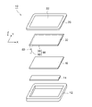
- FIG. 1 is an exploded perspective view of an electronic device 10 incorporating a sensor board group 18 as a board assembly according to the first embodiment of the present invention.
- the electronic device 10 may be various types of devices on which an electronic circuit board is mounted, such as a tablet computer used with an electronic pen.
- the electronic device 10 is configured by laminating a rear cover 12, a main board 14, a display panel 16, a sensor board group 18, and a front cover 20 in order from the rear side.
- the rear cover 12 and the front cover 20 are members forming a housing that accommodates electronic components in the electronic device 10 .
- the front cover 20 is provided with a highly translucent protective panel 22 so as to cover the entire opening formed on the main surface thereof.
- the main board 14 is a board that constitutes an electric circuit for operating the electronic device 10 .
- Various electronic components such as a host processor, memory, drive IC (Integrated Circuit) for the display panel 16, a connector for connecting to the sensor board group 18, a wireless communication module, and a power supply circuit are mounted on the main board 14. placed.
- the display panel 16 is composed of, for example, a liquid crystal panel, an organic EL (Electro Luminescence) panel, electronic paper, or the like.
- the display panel 16 displays an image or video in a display area by applying a driving voltage to a matrix of signal lines arranged in rows and columns to drive a plurality of pixels.
- the sensor board group 18 functions as an "external type" touch panel attached to the display panel 16 from the outside.
- the sensor substrate group 18 includes a detection substrate 30 (first substrate) having a pointing position detection function and a flexible substrate 50 (second substrate).
- the detection board 30 and the flexible board 50 are electrically connected without a connector.
- the detection substrate 30 has a touch sensor 32 capable of detecting the position indicated by the user's finger or electronic pen.
- the touch sensor 32 has linear or block-shaped sensor electrodes (not shown) arranged in a plane.
- touch control IC 52 An integrated circuit (hereinafter referred to as "touch control IC 52") that controls driving of the touch sensor 32 is mounted on the flexible substrate 50.
- This mounting method may be FOC (Chip on Film) or TAB (Tape Automated Bonding).
- the arrangement relationship between the display panel 16 and the sensor substrate group 18 is not limited to the example shown in FIG.
- the touch sensor 32 that employs the active electrostatic coupling method (AES) it is more preferable that the sensor substrate group 18 is provided above the display panel 16 .
- the touch sensor 32 that employs the electromagnetic induction method (EMR) it is more preferable that the sensor substrate group 18 is provided below the display panel 16 .
- FIG. 2 is a partial plan view of the sensor substrate group 18 shown in FIG. 3 is a cross-sectional view taken along line AA shown in FIG. 2.
- FIG. 2 directions are defined with reference to the position and orientation of the flexible substrate 50 . More specifically, the long-side direction, short-side direction, and height direction of the flexible substrate 50 are respectively referred to as a "length direction,” a "width direction,” and a “thickness direction.”
- the detection substrate 30 and the flexible substrate 50 are arranged such that both ends overlap each other.
- the detection substrate 30 is formed by laminating a substrate 34 on which a touch sensor 32 (FIG. 1) is mounted, a conductive layer 36, and an insulating layer 38 in this order.
- the base material 34 is made of an insulating and heat-resistant material (for example, a resin such as polyethylene terephthalate).
- the conductive layer 36 is made of a highly conductive material (for example, a metal such as copper, silver, or gold).
- the insulating layer 38 is provided so as to cover the entire surface of the conductive layer 36 except for the ends in the length direction (hereinafter referred to as the exposed tip portion 40).
- the flexible substrate 50 includes a substrate 54 on which a touch control IC 52 (FIGS. 1 and 2) is mounted, a conductive layer 56 provided on the bottom surface of the substrate 54, and a conductive layer 58 provided on the top surface of the substrate. And prepare.
- the base material 54 is made of an insulating, heat-resistant and flexible material (for example, a resin such as polyimide).
- the conductive layers 56 and 58 are made of highly conductive materials (for example, metals such as copper, silver, and gold).
- the protective film 68 is provided to protect the conductive layer 58 (more specifically, additional signal lines 64 and 66, which will be described later).
- ACF70 An anisotropic conductive film (hereinafter referred to as "ACF70") is interposed between the detection substrate 30 and the flexible substrate 50.
- the ACF 70 is formed by molding a mixed material in which fine metal particles are mixed into a thermosetting resin into a film.
- the detection substrate 30 and the flexible substrate 50 are crimped at a crimping portion 72 including the tip exposed portion 40 . That is, the application of heat and pressure at the crimped portion 72 forms a conductive region 74 that electrically connects the conductive layers 36 and 56 in a portion of the ACF 70 .
- a signal line group 44 (first signal line group) composed of a plurality of signal lines 42 is formed on the detection substrate 30 by the conductive layer 36 (FIG. 3).
- a signal line group 62 (second signal line group) composed of a plurality of signal lines 60 is formed on the flexible substrate 50 by a conductive layer 56 (FIG. 3).
- the plurality of signal lines 60 extend in the length direction and are arranged side by side in the width direction.
- the plurality of signal lines 42 extend in the length direction and are arranged side by side in the width direction.
- the signal lines 42 and 60 forming the two signal line groups 44 and 62 are aligned so as to be connected in a straight line.
- two additional signal lines 64 and 66 are formed on the flexible substrate 50 by the conductive layer 58 (FIG. 3).
- a part of the additional signal line 64 is provided extending in the width direction so as to cross the signal line group 44 at a position closer to the distal end than the crimped portion 72 in the length direction.
- a part of the additional signal line 66 is provided extending in the width direction so as to cross the signal line group 62 at a position on the rear end side of the crimped portion 72 in the length direction.
- Each signal line 42 is connected to a sensor electrode forming part of the touch sensor 32 (FIG. 1).
- Each signal line 60 is connected to a detection pin of the touch control IC 52 .
- Each additional signal line 64, 66 is connected to a test pin of the touch control IC 52, respectively.
- the electronic device 10 and the sensor board group 18 in the first embodiment are configured as described above.
- the connection state determination operation in the sensor board group 18 will be described with reference to FIGS. 2 to 4.
- the touch control IC 52 transmits a test signal via the first test pin. Then, a capacitive coupling CC (FIG. 3) is formed between the additional signal line 64 and the signal line 60 to generate a response signal to the test signal. The touch control IC 52 sequentially receives response signals via the signal line 60 . When the strength of the response signal exceeds the threshold, it is determined that "the first reception result is OK", and when the strength of the response signal is less than or equal to the threshold, it is determined that "the first reception result is N/A". .
- the touch control IC 52 transmits test signals via the second test pin. Then, a capacitive coupling CC (FIG. 3) is formed between the additional signal line 66 and the signal line 42 to generate a response signal to the test signal. Touch control IC 52 sequentially receives response signals via signal line 42 , conductive region 74 and signal line 60 . When the strength of the response signal exceeds the threshold, it is determined that "the second reception result is OK", and when the strength of the response signal is less than or equal to the threshold, it is determined that "the second reception result is N/A". .
- FIG. 4 is a diagram showing an example of a connection state determination method in the sensor board group 18 of FIGS.
- the sensor substrate group 18 (substrate assembly) in the first embodiment includes a plurality of signal lines 42 extending in the first direction and arranged side by side in a direction orthogonal to the first direction. It consists of a detection substrate 30 (first substrate) including a group 44 (first signal line group), and a plurality of signal lines 60 extending in the second direction and arranged side by side in a direction orthogonal to the second direction.
- the detection board 30 and the flexible board 50 are fixed so that the signal lines 42 and 60 constituting the signal line groups 44 and 62 are connected in a straight line. Additional signal lines 64 and 66 are provided on the flexible substrate 50 so as to extend across the signal line group 62 while being separated from the signal line group 62 in the thickness direction of the flexible substrate 50 .
- capacitive coupling CC is formed between each of the signal lines 60 forming the signal line group 62 and the additional signal lines 64 and 66. be.
- the connection state of the signal lines 60 can be identified. As a result, it is possible to inspect the connection state between the substrates with a simpler wiring structure.
- An ACF 70 (anisotropic conductive film) containing a thermosetting resin is interposed between the detection substrate 30 and the flexible substrate 50, and the ACF 70 is interposed between the detection substrate 30 and the flexible substrate 50. It may be fixed in a state of being thermally pressurized at the crimping portion 72 .
- At least one additional signal line 64 may be provided at a position closer to the distal end than the crimped portion 72 in the length direction (second direction).
- at least one additional signal line 66 may be provided on the flexible substrate 50 at a position on the rear end side of the crimped portion 72 in the length direction.
- at least two additional signal lines 66 may be provided on the flexible substrate 50 so as to sandwich the crimped portion 72 along the length direction.
- the signal line group 62 may be provided on one main surface of the flexible substrate 50 and the additional signal lines 64 and 66 may be provided on the other main surface of the flexible substrate 50 .
- the additional signal lines 64 and 66 can be arranged even at positions overlapping the signal line group 62 in plan view, and the degree of freedom in design is increased accordingly.
- the first substrate is the detection substrate 30 having the touch sensor 32
- the second substrate is the flexible substrate 50 having flexibility
- the touch sensor 32 is connected via the signal line groups 44 and 62. It may be connected to a touch control IC 52 (integrated circuit) for controlling the touch sensor 32 .
- a touch control IC 52 integrated circuit
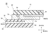
- FIG. 5 is a cross-sectional view of the sensor substrate group 80 in the first modified example of the first embodiment.
- the sensor substrate group 80 includes a detection substrate 30 (first substrate) having the same configuration as in the first embodiment, and a flexible substrate 82 (second substrate) different in configuration from the first embodiment. Prepare.
- the flexible substrate 82 includes a base material 84 on which the touch control IC 52 (FIGS. 1 and 2) is mounted, and a conductive layer 86 provided on the bottom surface of the base material 84.
- the base material 84 is made of an insulating, heat-resistant and flexible material (for example, a resin such as polyimide).
- the conductive layer 86 is made of a highly conductive material (for example, a metal such as copper, silver, or gold).
- a plurality of signal lines 42 (that is, a signal line group 44) are formed by the conductive layer 36 on the detection substrate 30, as in the first embodiment (FIG. 2).
- a plurality of signal lines 60 (that is, a signal line group 62) are formed on the flexible substrate 82 by a conductive layer 86. As shown in FIG. The signal lines 42 and 60 forming the signal line groups 44 and 62 are aligned so as to be connected in a straight line.
- one additional signal line 64 is formed on the flexible substrate 82 by a conductive layer 86 . A part of the additional signal line 64 is provided extending in the width direction so as to cross the signal line group 44 at a position on the tip side of the crimped portion 72 in the length direction.
- the signal line group 62 and the additional signal lines 64 may be provided on one main surface of the flexible substrate 50 .
- this configuration as in the case of the first embodiment, it is possible to inspect the connection state between the substrates with a simpler wiring structure.
- FIG. 6 is a cross-sectional view of the sensor substrate group 100 in the second modified example of the first embodiment.
- the sensor board group 100 includes a detection board 30 having the same configuration as in the first embodiment, a flexible board 102 (first board), and a main board 14 (second board).
- a signal line group 62 (first signal line group) consisting of a plurality of signal lines 60 and two additional signal lines 104 and 106 are formed on the flexible substrate 102, respectively. Also, the flexible substrate 102 and the main substrate 14 are crimped at a crimping portion 108 opposite to the crimping portion 72 .
- the signal lines 60 extend in the length direction and are arranged side by side in the width direction.
- a portion of the additional signal line 104 is provided extending in the width direction across the signal line group 62 at a position on the rear end side of the crimped portion 108 in the length direction.
- a part of the additional signal line 106 is provided extending in the width direction so as to cross the signal line group 62 at a position on the distal end side of the crimped portion 108 in the length direction.
- a touch control IC 52 On the other hand, on the main substrate 14, a touch control IC 52, a signal line group 112 (second signal line group) consisting of a plurality of signal lines 110, and two signal lines 114 and 116 are provided.
- the multiple signal lines 110 extend in the length direction and are arranged side by side in the width direction.
- the signal lines 42, 60, 110 forming the three signal line groups 44, 62, 112 are aligned so as to be connected in a straight line.
- Two additional signal lines 104, 106 are aligned to connect in line with signal lines 114, 116, respectively.
- Each signal line 42 is connected to a sensor electrode forming part of the touch sensor 32 (FIG. 1). Also, each signal line 110 is connected to a detection pin of the touch control IC 52 . The two signal lines 114 and 116 are connected to test pins of the touch control IC 52, respectively.
- the touch control IC 52 may be provided on a substrate (for example, the main substrate 14) different from the flexible substrate 102.
- a substrate for example, the main substrate 14
- the touch control IC 52 may be provided on a substrate (for example, the main substrate 14) different from the flexible substrate 102.
- the first embodiment (FIGS. 2 and 3) describes the case where the additional signal lines 64 and 66 extend across the signal line group 62 at right angles
- the arrangement of the additional signal lines is not limited to this.
- the flexible substrate 50 while being separated from the signal line group 62 in the thickness direction, it extends across a plurality of connection terminals (that is, a connection terminal group) connected to the signal line group 44 of the detection substrate 30 .
- Additional signal lines may be provided.
- the additional signal lines 64, 66 may extend to intersect at an angle of less than 90 degrees.
- the additional signal lines 64 and 66 are provided only on the flexible substrate 50
- the arrangement of the additional signal lines is not limited to this.
- the signal line group 44 (or the connection terminal group connected to the signal line group 62 of the flexible board 50) is provided while being separated from the signal line group 44 in the thickness direction of the detection board 30. Additional signal lines may be provided that extend across the . As a result, the connection state of the signal line 42 can also be inspected, making it easier to isolate the cause.
- the additional signal lines 64 and 66 are provided at positions sandwiching the crimped portion 72
- the arrangement of the additional signal lines is not limited to this.
- at least one additional signal line may be provided on the flexible substrate 50 at a location including the crimping site 73 . As a result, the connection state at the connecting portion of the signal lines 42 and 60 can be directly inspected.
- connection form of the additional signal lines is not limited to this.
- an input terminal may be provided on one end side of the additional signal line. For example, by connecting an external inspection device to the input terminal, it becomes easier to inspect the connection state.
- the touch control IC 52 transmits test signals from the additional signal lines 64 and 66 , but the operation of the touch control IC 52 may be reversed. Specifically, the touch control IC 52 may sequentially transmit test signals via the signal line 60 and receive response signals via the additional signal lines 64 and 66 .
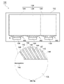
- FIG. 7 is a plan view of the display substrate 130 according to the second embodiment of the invention.
- This display substrate 130 functions as a "built-in type" (further classified, on-cell type or in-cell type) touch panel display in which a display panel and a touch sensor are integrated.
- the display substrate 130 includes a substrate 132, an integrated panel 136 composed of a plurality of divided panels 134, a control integrated circuit (hereinafter referred to as a control IC 138), and a plurality of signal line groups 140. be done.
- the base material 132 is made of an insulating and heat-resistant material (for example, glass).
- Integrated panel 136 , control ICs 138 and signal line group 140 are all disposed on one major surface (ie, surface) of substrate 132 .
- the number of control ICs 138 is equal to the number of divisions of the integrated panel 136 . That is, each divided panel 134 is connected to the corresponding control IC 138 via the signal line group 140 .
- signal lines 142 connected to the display panel side and signal lines 144 connected to the touch sensor side are arranged periodically at substantially equal intervals. Configured. Also, one additional signal line 146 is arranged on the substrate 132 for one control IC 138 . The additional signal lines 146 start from the test pins of the control IC 138 and extend laterally on the front surface of the substrate 132 . extending across the
- the display substrate 130 in the second embodiment is configured as described above. Next, the connection state determination operation of the display substrate 130 will be described. First, the control IC 138 periodically or irregularly starts a control mode (that is, a test mode) for inspecting the connection state of the display substrate 130 .
- a control mode that is, a test mode
- the display substrate 130 includes a base material 132, a signal line group 140 including a plurality of signal lines 142 and 144 provided on one main surface of the base material 132 and arranged side by side, and at least and one or more additional signal lines 146 partially provided on the other main surface of the substrate 132 and extending across the signal line group 140 .
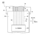
- FIG. 8 is a partial plan view of the sensor substrate group 200 according to the third embodiment.
- the sensor board group 200 includes a detection board 30 having the same configuration as in the first embodiment, and a flexible board 202 .
- the configuration of the flexible substrate 202 differs from that of the first embodiment (FIG. 2) in that additional signal lines 64 and 66 are not provided. Further, the flexible substrate 202 is provided with a touch control IC 204 having a function different from that of the first embodiment.
- the sensor substrate group 200 in the third embodiment is configured as described above.
- the connection state determination operation in the sensor board group 200 will be described.
- the touch control IC 204 periodically or irregularly starts a control mode (that is, a test mode) for inspecting the connection state of the sensor board group 200 .
- the touch control IC 204 transmits a test signal via the first detection pin when executing the test mode. Then, a response signal to the test signal is generated by forming a capacitive coupling CC between the first signal line 60 and the adjacent signal line 60 . The touch control IC 204 sequentially receives response signals via the signal line 60 . As a result, a response signal having a higher signal level is received closer to the first signal line 60 .
- the touch control IC 204 transmits test signals via the second detection pin and sequentially receives response signals via the adjacent signal line 60 . Thereafter, response signals are sequentially received while sequentially changing the signal line 60 for transmitting the test signal.
- FIG. 9 is a diagram showing an example of a connection state determination method in the sensor board group 200 of FIG.
- a connection state is assumed in which only the n-th signal line 60 among the N signal lines 60 is disconnected.
- response signals with signal levels exceeding the threshold are received from the adjacent (n-3)th and (n-1)th signal lines 60. be.
- a test signal is transmitted from the (n-1)th signal line 60
- a response signal whose signal level exceeds the threshold is received from the adjacent (n-2)th signal line 60, but A response signal whose signal level is equal to or less than the threshold value is received from the signal line 60 of .
- response signals whose signal levels are equal to or less than the threshold are received from the adjacent (n ⁇ 1)th and (n+1)th signal lines 60 .
- the touch control IC 204 can determine the connection state of the signal lines 60 by using the capacitive coupling CC formed between the adjacent signal lines 60 .
- the touch control IC 204 as a touch controller is connected to the signal line group 62 including a plurality of signal lines 60 arranged side by side.
- the touch control IC 204 transmits a test signal from one signal line 60, and transmits a response signal associated with the capacitive coupling CC formed between the signal lines 60 from another signal line 60 adjacent to the one signal line 60.
- the connection status of the signal line 60 may be determined based on the intensity of the response signal received.
- connection state of the sensor board group 200 can be inspected without providing additional signal lines 64 and 66 (FIGS. 2 and 3).
Landscapes
- Engineering & Computer Science (AREA)
- Microelectronics & Electronic Packaging (AREA)
- General Engineering & Computer Science (AREA)
- Theoretical Computer Science (AREA)
- Computer Networks & Wireless Communication (AREA)
- Human Computer Interaction (AREA)
- Physics & Mathematics (AREA)
- General Physics & Mathematics (AREA)
- Combinations Of Printed Boards (AREA)
Abstract
より簡易な配線構造でありながら基板同士の接続状態を検査可能な基板アセンブリ、基板、及び電子機器を提供する。基板アセンブリ(18)を構成する第1基板(30)と第2基板(50)とは、第1信号線群(44)及び第2信号線群(62)を構成する信号線(42,60)同士がそれぞれ一線状に繋がるように固定される。第2基板(50)上には、第2信号線群(62)から第2基板(50)の厚み方向に離間しつつ、第2信号線群(62)、又は、第1信号線群(44)に接続される複数の接続端子からなる第2接続端子群を横切るように延びる追加信号線(64,66)が設けられる。
Description
本発明は、基板アセンブリ、基板、及び電子機器に関する。
従来から、電子回路基板上に実装された信号線が断線しているか否かを検査する技術が知られている。例えば、特許文献1には、複数本のライン電極を二次元格子状に配置してなる静電容量方式のタッチセンサに関する検査方法が開示されている。
例えば、基板同士の接続時に、異方性導電膜(ACF;Anisotropic Conductive Film)を用いた圧着加工が用いられる場合がある。この圧着加工には、半田付けやコネクタによる接続と比べて、低背化や挟ピッチ化を図りやすいという利点がある。ところが、圧接作業に伴って接続不良や断線などが生じる可能性が高まる。
本発明はこのような問題に鑑みてなされたものであり、その目的は、より簡易な配線構造でありながら基板同士の接続状態を検査可能な基板アセンブリ、基板、及び電子機器を提供することにある。
第1の本発明における基板アセンブリは、第1方向に延びて、前記第1方向と直交する方向に並んで配置される複数本の信号線からなる第1信号線群を含む第1基板と、第2方向に延びて、前記第2方向と直交する方向に並んで配置される複数本の信号線からなる第2信号線群を含む第2基板と、を備え、前記第1基板と前記第2基板とは、前記第1信号線群及び前記第2信号線群を構成する信号線同士がそれぞれ一線状に繋がるように固定され、前記第2基板上には、前記第2信号線群から前記第2基板の厚み方向に離間しつつ、前記第2信号線群、又は、前記第1信号線群に接続される複数の接続端子である第2接続端子群を横切るように延びる追加信号線が設けられる。
第2の本発明における基板は、基材と、前記基材の一方の主面上に設けられ、並んで配置される複数本の信号線からなる信号線群、又は、並んで配置される複数の接続端子からなる接続端子群と、前記基材の他方の主面上に設けられ、前記信号線群又は前記接続端子群を横切るように延びる1本以上の追加信号線と、を備える。
第3の本発明における電子機器は、第1の本発明における基板アセンブリ又は第2の本発明における基板を備える。
本発明によれば、より簡易な配線構造でありながら基板同士の接続状態を検査することができる。
以下、添付図面を参照しながら本発明の実施形態について説明する。説明の理解を容易にするため、各図面において同一の構成要素に対しては可能な限り同一の符号を付して、重複する説明は省略する。なお、本発明は、以下の第1~第3実施形態及び変形例に限定されるものではなく、この発明の主旨を逸脱しない範囲で自由に変更できることは勿論である。あるいは、技術的に矛盾が生じない範囲で各々の構成を任意に組み合わせてもよい。
[第1実施形態]
本発明の第1実施形態における基板アセンブリ及び電子機器について、図1~図4を参照しながら説明する。
本発明の第1実施形態における基板アセンブリ及び電子機器について、図1~図4を参照しながら説明する。
<全体構成>
図1は、本発明の第1実施形態における基板アセンブリとしてのセンサ基板群18が組み込まれた電子機器10の分解斜視図である。電子機器10は、電子回路基板が搭載される様々な種類の機器であってもよく、例えば、電子ペンとともに用いられるタブレット型のコンピュータである。この電子機器10は、背面側から順に、背面カバー12と、メイン基板14と、表示パネル16と、センサ基板群18と、正面カバー20と、を積層して構成される。
図1は、本発明の第1実施形態における基板アセンブリとしてのセンサ基板群18が組み込まれた電子機器10の分解斜視図である。電子機器10は、電子回路基板が搭載される様々な種類の機器であってもよく、例えば、電子ペンとともに用いられるタブレット型のコンピュータである。この電子機器10は、背面側から順に、背面カバー12と、メイン基板14と、表示パネル16と、センサ基板群18と、正面カバー20と、を積層して構成される。
背面カバー12及び正面カバー20は、電子機器10内の電子部品を収容する筐体をなす部材である。正面カバー20には、その主面に形成された開口の全面を覆うように、透光性が高い保護パネル22が設けられている。
メイン基板14は、電子機器10を作動するための電気回路を構成する基板である。メイン基板14の上には、例えば、ホストプロセッサ、メモリ、表示パネル16の駆動IC(Integrated Circuit)、センサ基板群18と接続するためのコネクタ、無線通信モジュール、電源回路などの様々な電子部品が配置される。
表示パネル16は、例えば、液晶パネル、有機EL(Electro Luminescence)パネル、電子ペーパーなどによって構成される。表示パネル16は、行方向及び列方向に配列されたマトリクス状の信号線に駆動電圧を印加して複数の画素を駆動することで、表示領域内に画像又は映像を表示する。
センサ基板群18は、表示パネル16に対して外側から取り付ける「外付け型」のタッチパネルとして機能する。センサ基板群18は、指示位置の検出機能を有する検出用基板30(第1基板)と、可撓性を有するフレキシブル基板50(第2基板)と、を備える。ここで、検出用基板30とフレキシブル基板50とは、コネクタレスにより電気的に接続される。
検出用基板30は、ユーザの指や電子ペンによる指示位置を検出可能なタッチセンサ32を有する。タッチセンサ32は、線状又はブロック状のセンサ電極(不図示)が面状に配置されてなる。
フレキシブル基板50には、タッチセンサ32の駆動制御を行う集積回路(以下、「タッチ制御用IC52」という)が実装される。この実装方法は、FOC(Chip on Film)であってもよいし、TAB(Tape Automated Bonding)であってもよい。
なお、表示パネル16及びセンサ基板群18の配置関係は、図1の例に限られず、タッチセンサ32の検出方式に応じて変更されてもよい。例えば、アクティブ静電結合方式(AES)を採用するタッチセンサ32に関して、センサ基板群18が表示パネル16の上方に設けられることがより好ましい。一方、電磁誘導方式(EMR)を採用するタッチセンサ32に関して、センサ基板群18が表示パネル16の下方に設けられることがより好ましい。
<センサ基板群18の構成>
図2は、図1に示すセンサ基板群18の部分平面図である。図3は、図2に示すA-A線に沿った断面図である。以下、フレキシブル基板50の位置・姿勢を基準として方向を定義する。より具体的には、フレキシブル基板50の長辺方向、短辺方向、高さ方向をそれぞれ「長さ方向」、「幅方向」及び「厚み方向」という。
図2は、図1に示すセンサ基板群18の部分平面図である。図3は、図2に示すA-A線に沿った断面図である。以下、フレキシブル基板50の位置・姿勢を基準として方向を定義する。より具体的には、フレキシブル基板50の長辺方向、短辺方向、高さ方向をそれぞれ「長さ方向」、「幅方向」及び「厚み方向」という。
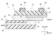
図3に示すように、検出用基板30とフレキシブル基板50とが、両方の端部同士が重なるように配置される。検出用基板30は、タッチセンサ32(図1)が実装された基材34と、導電層36と、絶縁層38と、が順次積層されてなる。基材34は、絶縁性及び耐熱性を有する材料(例えば、ポリエチレンテレフタレートなどの樹脂)からなる。導電層36は、導電性が高い材料(例えば、銅、銀、金などの金属)からなる。絶縁層38は、長さ方向の端部(以下、先端露出部40)を除き、導電層36の表面をすべて被覆するように設けられる。
一方、フレキシブル基板50は、タッチ制御用IC52(図1及び図2)が実装された基材54と、基材54の下面に設けられる導電層56と、基材の上面に設けられる導電層58と、を備える。基材54は、絶縁性、耐熱性及び可撓性を有する材料(例えば、ポリイミドなどの樹脂)からなる。導電層56,58は、導電性が高い材料(例えば、銅、銀、金などの金属)からなる。なお、保護膜68は、導電層58(より詳しくは、後述する追加信号線64,66)を保護するために設けられる。
検出用基板30とフレキシブル基板50の間には、異方性導電膜(以下、「ACF70」という)が介挿される。ACF70は、熱硬化性樹脂に微細な金属粒子を混ぜ合わせた混合材料を膜状に成型してなる。検出用基板30とフレキシブル基板50とが、先端露出部40を含む圧着部位72にて圧着される。つまり、圧着部位72にて加熱及び加圧が施されることで、ACF70の一部に、導電層36,56同士を電気的に接続する導電領域74が形成される。
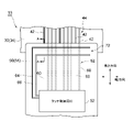
図2に示すように、検出用基板30上には、導電層36(図3)により、複数本の信号線42からなる信号線群44(第1信号線群)が形成される。フレキシブル基板50上には、導電層56(図3)により、複数本の信号線60からなる信号線群62(第2信号線群)が形成される。複数の信号線60は、長さ方向に延びるとともに、幅方向に並んで配置される。複数の信号線42は、長さ方向に延びるとともに、幅方向に並んで配置される。2つの信号線群44,62を構成する信号線42,60同士がそれぞれ一線状に繋がるように位置合わせされる。
さらに、フレキシブル基板50上には、導電層58(図3)により、2本の追加信号線64,66が形成される。追加信号線64の一部は、長さ方向に関して、圧着部位72よりも先端側の位置にて、信号線群44を横切るように幅方向に延びて設けられる。追加信号線66の一部は、長さ方向に関して、圧着部位72よりも後端側の位置にて、信号線群62を横切るように幅方向に延びて設けられる。
各々の信号線42は、タッチセンサ32(図1)の一部を構成するセンサ電極にそれぞれ接続される。また、各々の信号線60は、タッチ制御用IC52が有する検出用ピンにそれぞれ接続される。各々の追加信号線64,66は、タッチ制御用IC52が有するテスト用ピンにそれぞれ接続される。
<判定動作の説明>
第1実施形態における電子機器10及びセンサ基板群18は、以上のように構成される。続いて、このセンサ基板群18における接続状態の判定動作について、図2~図4を参照しながら説明する。まず、タッチ制御用IC52は、定期的又は不定期に、センサ基板群18の接続状態を検査するための制御モード(つまり、テストモード)を開始する。
第1実施形態における電子機器10及びセンサ基板群18は、以上のように構成される。続いて、このセンサ基板群18における接続状態の判定動作について、図2~図4を参照しながら説明する。まず、タッチ制御用IC52は、定期的又は不定期に、センサ基板群18の接続状態を検査するための制御モード(つまり、テストモード)を開始する。
テストモードの第1動作では、タッチ制御用IC52は、1番目のテスト用ピンを介してテスト信号を送信する。そうすると、追加信号線64と信号線60の間で容量結合CC(図3)が形成されることで、テスト信号に対する応答信号が発生する。タッチ制御用IC52は、信号線60を介して応答信号を順次受信する。応答信号の強度が閾値を上回った場合に「第1受信結果=OK」と判定される一方、応答信号の強度が閾値以下である場合に「第1受信結果=N/A」と判定される。
テストモードの第2動作では、タッチ制御用IC52は、2番目のテスト用ピンを介してテスト信号を送信する。そうすると、追加信号線66と信号線42との間で容量結合CC(図3)が形成されることで、テスト信号に対する応答信号が発生する。タッチ制御用IC52は、信号線42、導電領域74及び信号線60を介して、応答信号を順次受信する。応答信号の強度が閾値を上回った場合に「第2受信結果=OK」と判定される一方、応答信号の強度が閾値以下である場合に「第2受信結果=N/A」と判定される。
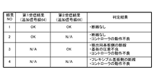
図4は、図2及び図3のセンサ基板群18における接続状態の判定方法の一例を示す図である。第1受信結果及び第2受信結果がいずれも「OK」である場合、検出用基板30の信号線42、フレキシブル基板50の信号線60の両方に断線がなく「正常」であると判定される(結果1)。一方、これ以外の結果の組み合わせ(結果2~4)である場合には「異常」であると判定されるとともに、以下の原因の切り分けが行われる。
第1受信結果のみが「OK」である場合、信号線42,60の断線はないが、タッチ制御用IC52の動作不良があると判定される(結果2)。第2受信結果のみが「OK」である場合、[1]信号線42の断線、[2]基板の圧着不良、又は[3]タッチ制御用IC52の動作不良のいずれかがあると判定される(結果3)。第1受信結果及び第2受信結果がいずれも「N/A」である場合、[1]信号線60の断線、又は[2]タッチ制御用IC52の動作不良のいずれかがあると判定される(結果4)。
<作用効果>
以上のように、第1実施形態におけるセンサ基板群18(基板アセンブリ)は、第1方向に延びて、第1方向と直交する方向に並んで配置される複数本の信号線42からなる信号線群44(第1信号線群)を含む検出用基板30(第1基板)と、第2方向に延びて、第2方向と直交する方向に並んで配置される複数本の信号線60からなる信号線群62(第2信号線群)を含むフレキシブル基板50(第2基板)と、を備える。検出用基板30とフレキシブル基板50とは、信号線群44,62を構成する信号線42,60同士がそれぞれ一線状に繋がるように固定される。フレキシブル基板50上には、信号線群62からフレキシブル基板50の厚み方向に離間しつつ、信号線群62を横切るように延びる追加信号線64,66が設けられる。
以上のように、第1実施形態におけるセンサ基板群18(基板アセンブリ)は、第1方向に延びて、第1方向と直交する方向に並んで配置される複数本の信号線42からなる信号線群44(第1信号線群)を含む検出用基板30(第1基板)と、第2方向に延びて、第2方向と直交する方向に並んで配置される複数本の信号線60からなる信号線群62(第2信号線群)を含むフレキシブル基板50(第2基板)と、を備える。検出用基板30とフレキシブル基板50とは、信号線群44,62を構成する信号線42,60同士がそれぞれ一線状に繋がるように固定される。フレキシブル基板50上には、信号線群62からフレキシブル基板50の厚み方向に離間しつつ、信号線群62を横切るように延びる追加信号線64,66が設けられる。
信号線群62を横切るように延びる追加信号線64,66を設けることで、信号線群62を構成する各々の信号線60と、追加信号線64,66との間に容量結合CCが形成される。例えば、追加信号線64,66からテスト信号を送信し、当該テスト信号に対する応答信号を各々の信号線60から受信することで、信号線60の接続状態を特定可能となる。これにより、より簡易な配線構造でありながら基板同士の接続状態を検査することができる。
また、検出用基板30とフレキシブル基板50との間には、熱硬化性樹脂を含有するACF70(異方性導電膜)が介在し、検出用基板30とフレキシブル基板50とは、ACF70が介在する圧着部位72にて熱加圧した状態で固定されてもよい。
また、フレキシブル基板50上には、長さ方向(第2方向)に関して圧着部位72よりも先端側の位置に、少なくとも1本の追加信号線64が設けられてもよい。また、フレキシブル基板50上には、長さ方向に関して圧着部位72よりも後端側の位置に、少なくとも1本の追加信号線66が設けられてもよい。また、フレキシブル基板50上には、長さ方向に沿って圧着部位72を挟むように、少なくとも2本の追加信号線66が設けられてもよい。
また、信号線群62は、フレキシブル基板50の一方の主面上に設けられ、追加信号線64,66は、フレキシブル基板50の他方の主面上に設けられてもよい。これにより、平面視にて信号線群62と重なる位置にも追加信号線64,66を配置可能となり、その分だけ設計の自由度が高くなる。
また、第1基板は、タッチセンサ32を有する検出用基板30であり、第2基板は、可撓性を有するフレキシブル基板50であり、タッチセンサ32は、信号線群44,62を介して、タッチセンサ32を制御するためのタッチ制御用IC52(集積回路)と接続されてもよい。特に、タッチ制御用IC52がフレキシブル基板50上に設けられることにより、基板のレイアウト設計の自由度がより高まる。
<第1変形例>
図5は、第1実施形態の第1変形例におけるセンサ基板群80の断面図である。このセンサ基板群80は、第1実施形態の場合と同様の構成を有する検出用基板30(第1基板)と、第1実施形態の構成とは異なるフレキシブル基板82(第2基板)と、を備える。
図5は、第1実施形態の第1変形例におけるセンサ基板群80の断面図である。このセンサ基板群80は、第1実施形態の場合と同様の構成を有する検出用基板30(第1基板)と、第1実施形態の構成とは異なるフレキシブル基板82(第2基板)と、を備える。
フレキシブル基板82は、タッチ制御用IC52(図1及び図2)が実装された基材84と、基材84の下面に設けられる導電層86と、を備える。基材84は、絶縁性、耐熱性及び可撓性を有する材料(例えば、ポリイミドなどの樹脂)からなる。導電層86は、導電性が高い材料(例えば、銅、銀、金などの金属)からなる。
検出用基板30上には、第1実施形態(図2)と同様に、導電層36により、複数本の信号線42(つまり、信号線群44)が形成される。フレキシブル基板82上には、導電層86により、複数本の信号線60(つまり、信号線群62)が形成される。信号線群44,62を構成する信号線42,60同士がそれぞれ一線状に繋がるように位置合わせされる。さらに、フレキシブル基板82上には、導電層86により、1本の追加信号線64が形成される。追加信号線64の一部は、長さ方向に関して圧着部位72よりも先端側の位置にて、信号線群44を横切るように幅方向に延びて設けられる。
このように、信号線群62及び追加信号線64が、フレキシブル基板50の一方の主面上に設けられてもよい。この構成によっても、第1実施形態の場合と同様に、より簡易な配線構造でありながら基板同士の接続状態を検査することができる。
<第2変形例>
図6は、第1実施形態の第2変形例におけるセンサ基板群100の断面図である。このセンサ基板群100は、第1実施形態の場合と同様の構成を有する検出用基板30と、フレキシブル基板102(第1基板)と、メイン基板14(第2基板)と、を備える。
図6は、第1実施形態の第2変形例におけるセンサ基板群100の断面図である。このセンサ基板群100は、第1実施形態の場合と同様の構成を有する検出用基板30と、フレキシブル基板102(第1基板)と、メイン基板14(第2基板)と、を備える。
フレキシブル基板102上には、複数本の信号線60からなる信号線群62(第1信号線群)と、2本の追加信号線104,106がそれぞれ形成される。また、フレキシブル基板102とメイン基板14とが、圧着部位72とは反対側の圧着部位108にて圧着される。
信号線60は、長さ方向に延びるとともに、幅方向に並んで配置される。追加信号線104の一部は、長さ方向に関して、圧着部位108よりも後端側の位置にて、信号線群62を横切るように幅方向に延びて設けられる。追加信号線106の一部は、長さ方向に関して、圧着部位108よりも先端側の位置にて、信号線群62を横切るように幅方向に延びて設けられる。
一方、メイン基板14上には、タッチ制御用IC52と、複数本の信号線110からなる信号線群112(第2信号線群)と、2本の信号線114,116と、が設けられる。複数本の信号線110は、長さ方向に延びるとともに、幅方向に並んで配置される。3つの信号線群44,62,112を構成する信号線42,60,110同士がそれぞれ一線状に繋がるように位置合わせされる。2本の追加信号線104,106は、信号線114,116とそれぞれ一線状に繋がるように位置合わせされる。
各々の信号線42は、タッチセンサ32(図1)の一部を構成するセンサ電極にそれぞれ接続される。また、各々の信号線110は、タッチ制御用IC52が有する検出用ピンにそれぞれ接続される。また、2本の信号線114,116は、タッチ制御用IC52が有するテスト用ピンにそれぞれ接続される。
このように、タッチ制御IC52が、フレキシブル基板102とは別の基板(例えば、メイン基板14)上に設けられてもよい。この構成によっても、第1実施形態の場合と同様に、より簡易な配線構造でありながら基板同士の接続状態を検査することができる。
<他の変形例>
第1実施形態(図2及び図3)では、追加信号線64,66が信号線群62を直交して横切るように延びる場合について説明したが、追加信号線の配置はこれに限られない。例えば、フレキシブル基板50上には、信号線群62から厚み方向に離間しつつ、検出用基板30の信号線群44に接続される複数の接続端子(つまり、接続端子群)を横切るように延びる追加信号線が設けられてもよい。また、追加信号線64,66は、90度よりも小さい角度で交差するように延びてもよい。
第1実施形態(図2及び図3)では、追加信号線64,66が信号線群62を直交して横切るように延びる場合について説明したが、追加信号線の配置はこれに限られない。例えば、フレキシブル基板50上には、信号線群62から厚み方向に離間しつつ、検出用基板30の信号線群44に接続される複数の接続端子(つまり、接続端子群)を横切るように延びる追加信号線が設けられてもよい。また、追加信号線64,66は、90度よりも小さい角度で交差するように延びてもよい。
第1実施形態(図2及び図3)では、フレキシブル基板50のみに追加信号線64,66が設けられる場合について説明したが、追加信号線の配置はこれに限られない。例えば、検出用基板30上には、信号線群44から検出用基板30の厚み方向に離間しつつ、信号線群44(又は、フレキシブル基板50の信号線群62に接続される接続端子群)を横切るように延びる追加信号線が設けられてもよい。これにより、信号線42の接続状態も併せて検査可能となり、その分だけ原因の切り分けが行いやすくなる。
第1実施形態(図2及び図3)では、追加信号線64,66が圧着部位72を挟む位置に設けられる場合について説明したが、追加信号線の配置はこれに限られない。例えば、フレキシブル基板50上には、圧着部位73を含む位置に、少なくとも1本の追加信号線が設けられてもよい。これにより、信号線42,60の連結部分における接続状態を直接的に検査することができる。
第1実施形態(図2)では、追加信号線64,66がタッチ制御用IC52に接続される場合について説明したが、追加信号線の接続形態はこれに限られない。例えば、追加信号線の一端側には入力端子が設けられてもよい。例えば、外付けの検査装置を入力端子に接続することで、接続状態の検査が行いやすくなる。
第1実施形態(図4)では、タッチ制御用IC52が追加信号線64,66からテスト信号を送信する場合について説明したが、タッチ制御用IC52の動作がこの逆であってもよい。具体的には、タッチ制御用IC52は、信号線60を介してテスト信号を順次送信し、追加信号線64,66を介して応答信号を受信してもよい。
[第2実施形態]
<表示用基板130の構成>
図7は、本発明の第2実施形態における表示用基板130の平面図である。この表示用基板130は、表示パネルとタッチセンサとが一体的に構成される「内蔵型」(さらに分類すると、オンセル型又はインセル型)のタッチパネルディスプレイとして機能する。この表示用基板130は、基材132と、複数の分割パネル134からなる一体型パネル136と、制御用集積回路(以下、制御用IC138)と、複数の信号線群140と、を含んで構成される。
<表示用基板130の構成>
図7は、本発明の第2実施形態における表示用基板130の平面図である。この表示用基板130は、表示パネルとタッチセンサとが一体的に構成される「内蔵型」(さらに分類すると、オンセル型又はインセル型)のタッチパネルディスプレイとして機能する。この表示用基板130は、基材132と、複数の分割パネル134からなる一体型パネル136と、制御用集積回路(以下、制御用IC138)と、複数の信号線群140と、を含んで構成される。
基材132は、絶縁性及び耐熱性を有する材料(例えば、ガラス)からなる。一体型パネル136、制御用IC138及び信号線群140はいずれも、基材132の一方の主面(つまり、表面)に配置される。制御用IC138の個数は、一体型パネル136の分割数に等しい。すなわち、各々の分割パネル134は、信号線群140を介して、対応する制御用IC138と接続される。
部分Bの拡大図に示すように、信号線群140は、表示パネル側に接続される信号線142と、タッチセンサ側に接続される信号線144と、が略等間隔かつ周期的に並んで構成される。また、基材132上には、1つの制御用IC138につき、1本の追加信号線146が配置される。追加信号線146は、制御用IC138のテスト用ピンを起点として、基材132の表面上にて横方向に延び、図示しないスルーホールを介して、基材132の裏面上にて信号線群140を横切るように延びる。
<判定動作の説明>
第2実施形態における表示用基板130は、以上のように構成される。続いて、この表示用基板130における接続状態の判定動作について説明する。まず、制御用IC138は、定期的又は不定期に、表示用基板130の接続状態を検査するための制御モード(つまり、テストモード)を開始する。
第2実施形態における表示用基板130は、以上のように構成される。続いて、この表示用基板130における接続状態の判定動作について説明する。まず、制御用IC138は、定期的又は不定期に、表示用基板130の接続状態を検査するための制御モード(つまり、テストモード)を開始する。
制御用IC138は、テストモードの実行時に、テスト用ピンを介してテスト信号を送信する。そうすると、追加信号線146と信号線144の間で容量結合CCが形成されることで、テスト信号に対する応答信号が発生する。制御用IC138は、信号線144を介して応答信号を順次受信する。応答信号の強度が閾値を上回った場合に「受信結果=OK」であるとして信号線144の断線がないと判定される。一方、応答信号の強度が閾値以下である場合に「受信結果=N/A」であるとして信号線144の断線があると判定される。
<作用効果>
このように、表示用基板130は、基材132と、基材132の一方の主面上に設けられ、並んで配置される複数本の信号線142,144からなる信号線群140と、少なくとも一部が基材132の他方の主面上に設けられ、信号線群140を横切るように延びる1本以上の追加信号線146と、を備える。
このように、表示用基板130は、基材132と、基材132の一方の主面上に設けられ、並んで配置される複数本の信号線142,144からなる信号線群140と、少なくとも一部が基材132の他方の主面上に設けられ、信号線群140を横切るように延びる1本以上の追加信号線146と、を備える。
この構成によっても、第1実施形態の場合と同様に、より簡易な配線構造でありながら表示用基板130の接続状態を検査することができる。
[第3実施形態]
続いて、第3実施形態における基板アセンブリ及びその接続状態の検査方法について、図8及び図9を参照しながら説明する。
続いて、第3実施形態における基板アセンブリ及びその接続状態の検査方法について、図8及び図9を参照しながら説明する。
<センサ基板群200の構成>
図8は、第3実施形態におけるセンサ基板群200の部分平面図である。センサ基板群200は、第1実施形態の場合と同様の構成を有する検出用基板30と、フレキシブル基板202と、を備える。フレキシブル基板202は、追加信号線64,66が設けられない点で第1実施形態(図2)とは構成が異なる。また、フレキシブル基板202には、第1実施形態とは機能が異なるタッチ制御用IC204が設けられる。
図8は、第3実施形態におけるセンサ基板群200の部分平面図である。センサ基板群200は、第1実施形態の場合と同様の構成を有する検出用基板30と、フレキシブル基板202と、を備える。フレキシブル基板202は、追加信号線64,66が設けられない点で第1実施形態(図2)とは構成が異なる。また、フレキシブル基板202には、第1実施形態とは機能が異なるタッチ制御用IC204が設けられる。
<判定動作の説明>
第3実施形態におけるセンサ基板群200は、以上のように構成される。続いて、このセンサ基板群200における接続状態の判定動作について説明する。まず、タッチ制御用IC204は、定期的又は不定期に、センサ基板群200の接続状態を検査するための制御モード(つまり、テストモード)を開始する。
第3実施形態におけるセンサ基板群200は、以上のように構成される。続いて、このセンサ基板群200における接続状態の判定動作について説明する。まず、タッチ制御用IC204は、定期的又は不定期に、センサ基板群200の接続状態を検査するための制御モード(つまり、テストモード)を開始する。
タッチ制御用IC204は、テストモードの実行時に、1番目の検出用ピンを介してテスト信号を送信する。そうすると、1番目の信号線60とその近傍にある信号線60の間で容量結合CCが形成されることで、テスト信号に対する応答信号が発生する。タッチ制御用IC204は、信号線60を介して応答信号を順次受信する。その結果、1番目の信号線60に近いほど信号レベルが高い応答信号が受信される。
次いで、タッチ制御用IC204は、2番目の検出用ピンを介してテスト信号を送信し、隣接する信号線60を介して応答信号を順次受信する。以下、テスト信号を送信する信号線60を順次変更しながら応答信号を順次受信する。
図9は、図8のセンサ基板群200における接続状態の判定方法の一例を示す図である。ここでは、N本の信号線60のうち、n番目の信号線60のみが断線している接続状態を想定する。(n-2)番目の信号線60からテスト信号が送信された場合、隣接する(n-3)番目、(n-1)番目の信号線60から信号レベルが閾値を上回る応答信号が受信される。(n-1)番目の信号線60からテスト信号が送信された場合、隣接する(n-2)番目の信号線60から信号レベルが閾値を上回る応答信号が受信されるが、隣接するn番目の信号線60から信号レベルが閾値以下の応答信号が受信される。n番目の信号線からテスト信号が送信された場合、隣接する(n-1)番目、(n+1)番目の信号線60から信号レベルが閾値以下の応答信号が受信される。
このようにして、タッチ制御用IC204は、隣接する信号線60間で形成される容量結合CCを利用して、信号線60の接続状態を判定することができる。
<作用効果>
以上のように、タッチコントローラとしてのタッチ制御用IC204は、並んで配置される複数本の信号線60からなる信号線群62に接続される。そして、タッチ制御用IC204は、一の信号線60からテスト信号を送信し、信号線60間で形成される容量結合CCに伴う応答信号を一の信号線60と隣り合う他の信号線60から受信し、応答信号の強度に基づいて信号線60の接続状態を判定してもよい。
以上のように、タッチコントローラとしてのタッチ制御用IC204は、並んで配置される複数本の信号線60からなる信号線群62に接続される。そして、タッチ制御用IC204は、一の信号線60からテスト信号を送信し、信号線60間で形成される容量結合CCに伴う応答信号を一の信号線60と隣り合う他の信号線60から受信し、応答信号の強度に基づいて信号線60の接続状態を判定してもよい。
このように構成することで、追加信号線64,66(図2及び図3)を設けずに、センサ基板群200の接続状態を検査することができる。
[符号の説明]
10…電子機器、18,80,100,200…センサ基板群(基板アセンブリ)、30…検出用基板、50,82,202…フレキシブル基板、44,62,112,140…信号線群、64,66,104,106,146…追加信号線、130…表示用基板(基板)
10…電子機器、18,80,100,200…センサ基板群(基板アセンブリ)、30…検出用基板、50,82,202…フレキシブル基板、44,62,112,140…信号線群、64,66,104,106,146…追加信号線、130…表示用基板(基板)
Claims (13)
- 第1方向に延びて、前記第1方向と直交する方向に並んで配置される複数本の信号線からなる第1信号線群を含む第1基板と、
第2方向に延びて、前記第2方向と直交する方向に並んで配置される複数本の信号線からなる第2信号線群を含む第2基板と、
を備え、
前記第1基板と前記第2基板とは、前記第1信号線群及び前記第2信号線群を構成する信号線同士がそれぞれ一線状に繋がるように固定され、
前記第2基板上には、前記第2信号線群から前記第2基板の厚み方向に離間しつつ、前記第2信号線群、又は、前記第1信号線群に接続される複数の接続端子からなる第2接続端子群を横切るように延びる追加信号線が設けられる、基板アセンブリ。 - 前記第1基板上には、前記第1信号線群から前記第1基板の厚み方向に離間しつつ、前記第1信号線群、又は、前記第2信号線群に接続される複数の接続端子からなる第1接続端子群を横切るように延びる追加信号線が設けられる、
請求項1に記載の基板アセンブリ。 - 前記第1基板と前記第2基板との間には、熱硬化性樹脂を含有する異方性導電膜が介在し、
前記第1基板と前記第2基板とは、前記異方性導電膜が介在する圧着部位にて熱加圧した状態で固定される、
請求項1に記載の基板アセンブリ。 - 前記第2基板上には、前記第2方向に関して前記圧着部位よりも先端側の位置に、少なくとも1本の追加信号線が設けられる、
請求項3に記載の基板アセンブリ。 - 前記第2基板上には、前記第2方向に関して前記圧着部位よりも後端側の位置に、少なくとも1本の追加信号線が設けられる、
請求項3に記載の基板アセンブリ。 - 前記第2基板上には、前記圧着部位を含む位置に、少なくとも1本の追加信号線が設けられる、
請求項3に記載の基板アセンブリ。 - 前記第2基板上には、前記第2方向に沿って前記圧着部位を挟むように、少なくとも2本の追加信号線が設けられる、
請求項3に記載の基板アセンブリ。 - 前記第2信号線群は、前記第2基板の一方の主面上に設けられ、
前記追加信号線は、前記第2基板の他方の主面上に設けられる、
請求項1に記載の基板アセンブリ。 - 前記第2信号線群及び前記追加信号線は、前記第2基板の一方の主面上に設けられる、
請求項1に記載の基板アセンブリ。 - 前記第1基板は、タッチセンサを有する検出用基板であり、
前記第2基板は、可撓性を有するフレキシブル基板であり、
前記タッチセンサは、前記第1信号線群及び前記第2信号線群を介して、前記タッチセンサを制御するための集積回路と接続される、
請求項1に記載の基板アセンブリ。 - 前記集積回路は、前記フレキシブル基板上に設けられる、
請求項10に記載の基板アセンブリ。 - 基材と、
前記基材の一方の主面上に設けられ、並んで配置される複数本の信号線からなる信号線群、又は、並んで配置される複数の接続端子からなる接続端子群と、
前記基材の他方の主面上に設けられ、前記信号線群又は前記接続端子群を横切るように延びる1本以上の追加信号線と、
を備える、基板。 - 請求項1~11のいずれか1項に記載の基板アセンブリを備える電子機器。
Priority Applications (4)
| Application Number | Priority Date | Filing Date | Title |
|---|---|---|---|
| CN202180057006.0A CN116034331A (zh) | 2021-03-22 | 2021-03-22 | 基板组件、基板及电子设备 |
| JP2023508149A JP7620083B2 (ja) | 2021-03-22 | 2021-03-22 | 基板アセンブリ、基板、及び電子機器 |
| PCT/JP2021/011624 WO2022201224A1 (ja) | 2021-03-22 | 2021-03-22 | 基板アセンブリ、基板、及び電子機器 |
| US18/457,115 US12628275B2 (en) | 2021-03-22 | 2023-08-28 | Board assembly, board, and electronic device |
Applications Claiming Priority (1)
| Application Number | Priority Date | Filing Date | Title |
|---|---|---|---|
| PCT/JP2021/011624 WO2022201224A1 (ja) | 2021-03-22 | 2021-03-22 | 基板アセンブリ、基板、及び電子機器 |
Related Child Applications (1)
| Application Number | Title | Priority Date | Filing Date |
|---|---|---|---|
| US18/457,115 Continuation US12628275B2 (en) | 2021-03-22 | 2023-08-28 | Board assembly, board, and electronic device |
Publications (1)
| Publication Number | Publication Date |
|---|---|
| WO2022201224A1 true WO2022201224A1 (ja) | 2022-09-29 |
Family
ID=83395374
Family Applications (1)
| Application Number | Title | Priority Date | Filing Date |
|---|---|---|---|
| PCT/JP2021/011624 Ceased WO2022201224A1 (ja) | 2021-03-22 | 2021-03-22 | 基板アセンブリ、基板、及び電子機器 |
Country Status (4)
| Country | Link |
|---|---|
| US (1) | US12628275B2 (ja) |
| JP (1) | JP7620083B2 (ja) |
| CN (1) | CN116034331A (ja) |
| WO (1) | WO2022201224A1 (ja) |
Families Citing this family (2)
| Publication number | Priority date | Publication date | Assignee | Title |
|---|---|---|---|---|
| JP1739138S (ja) * | 2022-07-15 | 2023-03-16 | ||
| JP1734693S (ja) * | 2022-07-15 | 2023-01-17 |
Citations (3)
| Publication number | Priority date | Publication date | Assignee | Title |
|---|---|---|---|---|
| JP2003262884A (ja) * | 2002-03-08 | 2003-09-19 | Matsushita Electric Ind Co Ltd | 液晶表示装置 |
| JP2018092320A (ja) * | 2016-12-01 | 2018-06-14 | 株式会社ジャパンディスプレイ | 検出装置 |
| JP2018200572A (ja) * | 2017-05-26 | 2018-12-20 | 株式会社ジャパンディスプレイ | 表示装置 |
Family Cites Families (17)
| Publication number | Priority date | Publication date | Assignee | Title |
|---|---|---|---|---|
| US4561709A (en) * | 1983-12-09 | 1985-12-31 | Amp Incorporated | Membrane type circuit having improved tail |
| US6052172A (en) * | 1996-05-29 | 2000-04-18 | Enplas Corporation | Contacting device for display panel |
| US7528327B2 (en) * | 2005-04-28 | 2009-05-05 | Semiconductor Energy Laboratory Co., Ltd. | Inspection method and semiconductor device |
| JP2008089819A (ja) * | 2006-09-29 | 2008-04-17 | Toshiba Matsushita Display Technology Co Ltd | フレキシブル基板及びフレキシブル基板を備えた表示装置 |
| US8456851B2 (en) * | 2008-05-16 | 2013-06-04 | Apple Inc. | Flex circuit with single sided routing and double sided attach |
| WO2010035557A1 (ja) * | 2008-09-29 | 2010-04-01 | シャープ株式会社 | 表示パネル |
| KR100935499B1 (ko) * | 2009-01-08 | 2010-01-06 | 이성호 | 터치 패널 |
| JP5334197B2 (ja) * | 2009-12-15 | 2013-11-06 | 株式会社ジャパンディスプレイ | 静電容量型入力装置、静電容量型入力装置の検査方法、静電容量型入力装置用駆動装置 |
| JP5561697B2 (ja) * | 2010-07-02 | 2014-07-30 | Fdk株式会社 | 防爆機能付き蓄電セル、防爆機能付き蓄電モジュール |
| JP2019117315A (ja) * | 2017-12-27 | 2019-07-18 | シャープ株式会社 | 表示装置、表示装置の製造方法、及び、表示装置の検査方法。 |
| JP7156893B2 (ja) | 2018-02-22 | 2022-10-19 | 株式会社ワコム | 位置検出回路及び位置検出方法 |
| CN108803166B (zh) * | 2018-07-06 | 2021-05-25 | 京东方科技集团股份有限公司 | 一种基板组件、显示面板及显示装置 |
| KR102620548B1 (ko) * | 2018-07-09 | 2024-01-03 | 삼성전자주식회사 | 신호 배선을 둘러싸는 복수의 그라운드 배선들이 배치된 연성 회로기판을 포함하는 전자 장치 |
| KR102078855B1 (ko) * | 2019-01-03 | 2020-02-19 | 동우 화인켐 주식회사 | 터치 센서 모듈, 이를 포함하는 윈도우 적층체 및 이를 포함하는 화상 표시 장치 |
| CN113391715B (zh) * | 2020-03-13 | 2023-07-21 | 京东方科技集团股份有限公司 | 显示装置 |
| CN111511098B (zh) * | 2020-06-10 | 2021-08-20 | 京东方科技集团股份有限公司 | 一种柔性线路板fpc及显示装置 |
| CN114982386B (zh) * | 2020-12-25 | 2025-03-28 | 京东方科技集团股份有限公司 | 柔性电路板及显示装置 |
-
2021
- 2021-03-22 WO PCT/JP2021/011624 patent/WO2022201224A1/ja not_active Ceased
- 2021-03-22 JP JP2023508149A patent/JP7620083B2/ja active Active
- 2021-03-22 CN CN202180057006.0A patent/CN116034331A/zh active Pending
-
2023
- 2023-08-28 US US18/457,115 patent/US12628275B2/en active Active
Patent Citations (3)
| Publication number | Priority date | Publication date | Assignee | Title |
|---|---|---|---|---|
| JP2003262884A (ja) * | 2002-03-08 | 2003-09-19 | Matsushita Electric Ind Co Ltd | 液晶表示装置 |
| JP2018092320A (ja) * | 2016-12-01 | 2018-06-14 | 株式会社ジャパンディスプレイ | 検出装置 |
| JP2018200572A (ja) * | 2017-05-26 | 2018-12-20 | 株式会社ジャパンディスプレイ | 表示装置 |
Also Published As
| Publication number | Publication date |
|---|---|
| CN116034331A (zh) | 2023-04-28 |
| US20230403794A1 (en) | 2023-12-14 |
| US12628275B2 (en) | 2026-05-12 |
| JP7620083B2 (ja) | 2025-01-22 |
| JPWO2022201224A1 (ja) | 2022-09-29 |
Similar Documents
| Publication | Publication Date | Title |
|---|---|---|
| JP4711149B2 (ja) | フレキシブルプリント配線板、タッチパネル、表示パネルおよび表示装置 | |
| US20120146919A1 (en) | Touch screen panel | |
| US20150317013A1 (en) | Touch sensor with integrated signal bus extensions | |
| TWI715831B (zh) | 觸控面板及穿戴式裝置 | |
| CN112684939B (zh) | 用于窄边框电子设备的触控屏和电子设备 | |
| WO2019026649A1 (ja) | ペンが送信したペン信号を検出するためのセンサ | |
| CN103765355A (zh) | 柔性电路路由 | |
| CN111511109B (zh) | 柔性电路板及制作方法、电子装置模组及电子装置 | |
| CN114721546B (zh) | 一种触控显示面板和触控显示装置 | |
| KR102431147B1 (ko) | 터치 패널 및 이를 포함하는 표시 장치 | |
| WO2020156595A9 (zh) | 柔性电路板及制作方法、显示装置、电路板结构及其显示面板 | |
| CN113009740B (zh) | 显示面板及显示装置 | |
| US12628275B2 (en) | Board assembly, board, and electronic device | |
| JP5382357B2 (ja) | タッチパネル部材およびタッチパネル | |
| US9236200B2 (en) | Touch window and manufacturing method thereof | |
| US7683496B2 (en) | Misalignment detection devices | |
| KR20120006792A (ko) | 회로기판을 이용하여 터치센서 칩에 감지 신호를 전달하는 접촉 감지 패널 및 접촉 감지 장치 | |
| KR102388802B1 (ko) | 터치표시장치 | |
| CN106484165B (zh) | 触控面板及其制造方法 | |
| CN106886325B (zh) | 触控面板与电子装置 | |
| TWM466446U (zh) | 電性連接組件 | |
| TWI396004B (zh) | 電子裝置 | |
| JP2007200177A (ja) | 電子装置 | |
| KR100469356B1 (ko) | 터치패널 검사용 지그 | |
| US11360623B2 (en) | Touch sensor and electronic device |
Legal Events
| Date | Code | Title | Description |
|---|---|---|---|
| 121 | Ep: the epo has been informed by wipo that ep was designated in this application |
Ref document number: 21932841 Country of ref document: EP Kind code of ref document: A1 |
|
| ENP | Entry into the national phase |
Ref document number: 2023508149 Country of ref document: JP Kind code of ref document: A |
|
| NENP | Non-entry into the national phase |
Ref country code: DE |
|
| 122 | Ep: pct application non-entry in european phase |
Ref document number: 21932841 Country of ref document: EP Kind code of ref document: A1 |