WO2022196402A1 - 電磁波シールドシートおよびその製造方法、シールド性配線基板、並びに電子機器 - Google Patents
電磁波シールドシートおよびその製造方法、シールド性配線基板、並びに電子機器 Download PDFInfo
- Publication number
- WO2022196402A1 WO2022196402A1 PCT/JP2022/009527 JP2022009527W WO2022196402A1 WO 2022196402 A1 WO2022196402 A1 WO 2022196402A1 JP 2022009527 W JP2022009527 W JP 2022009527W WO 2022196402 A1 WO2022196402 A1 WO 2022196402A1
- Authority
- WO
- WIPO (PCT)
- Prior art keywords
- layer
- sheet
- conductive filler
- electromagnetic wave
- adhesive layer
- Prior art date
- Legal status (The legal status is an assumption and is not a legal conclusion. Google has not performed a legal analysis and makes no representation as to the accuracy of the status listed.)
- Ceased
Links
Images


Classifications
-
- H—ELECTRICITY
- H05—ELECTRIC TECHNIQUES NOT OTHERWISE PROVIDED FOR
- H05K—PRINTED CIRCUITS; CASINGS OR CONSTRUCTIONAL DETAILS OF ELECTRIC APPARATUS; MANUFACTURE OF ASSEMBLAGES OF ELECTRICAL COMPONENTS
- H05K9/00—Screening of apparatus or components against electric or magnetic fields
- H05K9/0073—Shielding materials
- H05K9/0081—Electromagnetic shielding materials, e.g. EMI, RFI shielding
- H05K9/0084—Electromagnetic shielding materials, e.g. EMI, RFI shielding comprising a single continuous metallic layer on an electrically insulating supporting structure, e.g. metal foil, film, plating coating, electro-deposition, vapour-deposition
-
- B—PERFORMING OPERATIONS; TRANSPORTING
- B32—LAYERED PRODUCTS
- B32B—LAYERED PRODUCTS, i.e. PRODUCTS BUILT-UP OF STRATA OF FLAT OR NON-FLAT, e.g. CELLULAR OR HONEYCOMB, FORM
- B32B27/00—Layered products comprising a layer of synthetic resin
- B32B27/18—Layered products comprising a layer of synthetic resin characterised by the use of special additives
-
- B—PERFORMING OPERATIONS; TRANSPORTING
- B32—LAYERED PRODUCTS
- B32B—LAYERED PRODUCTS, i.e. PRODUCTS BUILT-UP OF STRATA OF FLAT OR NON-FLAT, e.g. CELLULAR OR HONEYCOMB, FORM
- B32B7/00—Layered products characterised by the relation between layers; Layered products characterised by the relative orientation of features between layers, or by the relative values of a measurable parameter between layers, i.e. products comprising layers having different physical, chemical or physicochemical properties; Layered products characterised by the interconnection of layers
- B32B7/02—Physical, chemical or physicochemical properties
- B32B7/025—Electric or magnetic properties
-
- B—PERFORMING OPERATIONS; TRANSPORTING
- B32—LAYERED PRODUCTS
- B32B—LAYERED PRODUCTS, i.e. PRODUCTS BUILT-UP OF STRATA OF FLAT OR NON-FLAT, e.g. CELLULAR OR HONEYCOMB, FORM
- B32B7/00—Layered products characterised by the relation between layers; Layered products characterised by the relative orientation of features between layers, or by the relative values of a measurable parameter between layers, i.e. products comprising layers having different physical, chemical or physicochemical properties; Layered products characterised by the interconnection of layers
- B32B7/04—Interconnection of layers
- B32B7/12—Interconnection of layers using interposed adhesives or interposed materials with bonding properties
-
- H—ELECTRICITY
- H05—ELECTRIC TECHNIQUES NOT OTHERWISE PROVIDED FOR
- H05K—PRINTED CIRCUITS; CASINGS OR CONSTRUCTIONAL DETAILS OF ELECTRIC APPARATUS; MANUFACTURE OF ASSEMBLAGES OF ELECTRICAL COMPONENTS
- H05K1/00—Printed circuits
- H05K1/02—Details
-
- H—ELECTRICITY
- H05—ELECTRIC TECHNIQUES NOT OTHERWISE PROVIDED FOR
- H05K—PRINTED CIRCUITS; CASINGS OR CONSTRUCTIONAL DETAILS OF ELECTRIC APPARATUS; MANUFACTURE OF ASSEMBLAGES OF ELECTRICAL COMPONENTS
- H05K1/00—Printed circuits
- H05K1/02—Details
- H05K1/0213—Electrical arrangements not otherwise provided for
- H05K1/0216—Reduction of cross-talk, noise or electromagnetic interference
-
- H—ELECTRICITY
- H05—ELECTRIC TECHNIQUES NOT OTHERWISE PROVIDED FOR
- H05K—PRINTED CIRCUITS; CASINGS OR CONSTRUCTIONAL DETAILS OF ELECTRIC APPARATUS; MANUFACTURE OF ASSEMBLAGES OF ELECTRICAL COMPONENTS
- H05K9/00—Screening of apparatus or components against electric or magnetic fields
Definitions
- the present invention relates to an electromagnetic shielding sheet having an adhesive layer and a shielding layer and a method for producing the same.
- the present invention also relates to shielding wiring boards and electronic devices.
- Various electronic devices such as mobile terminals, PCs, servers, etc., contain substrates such as printed wiring boards. These substrates are provided with an electromagnetic wave shield structure to prevent malfunction due to external magnetic fields and radio waves and to reduce unwanted radiation from electrical signals.
- Patent Document 1 the problem is to provide a shielding film for printed wiring boards in which the metal layer is unlikely to break due to repeated bending and sliding, and the insulating film has an arithmetic mean roughness of 0.5 to 5.0 ⁇ m on one side
- a printed wiring board shielding film is disclosed comprising a layer and a metal layer formed in a bellows structure along the aforementioned one-sided surface of the insulating layer.
- Patent Document 2 the object is to provide an electromagnetic wave shielding film having sufficient bending resistance and whose shielding properties are unlikely to deteriorate when a shield printed wiring board is manufactured.
- Patent Document 3 discloses a conductive layer having a laminated structure of at least a conductive adhesive layer/electromagnetic wave absorbing layer/electromagnetic wave shielding layer (metal layer) from the flexible printed wiring board 50 side.
- Patent Document 4 discloses a shape-retaining film that includes a plastically deformable metal layer and an adhesive layer that adheres to a flexible wiring board, and that can be used as a shield film.
- a typical substance that blocks electromagnetic waves is a metal, and in the electromagnetic wave shielding film of Patent Document 1 and the like, the metal layer functions as a shield layer that blocks electromagnetic waves.
- the electromagnetic wave shielding sheet is usually wound into a roll during manufacture and stored, and then unwound during use. Also, in use, the electromagnetic wave shield sheet may be stamped into a desired size and shape.
- stress is accumulated in the electromagnetic shielding sheet during storage in a roll, causing residual strain, and warping (hereinafter referred to as curling) occurs in the electromagnetic shielding sheet when it is unwound.
- edge surface of the electromagnetic wave shielding sheet tends to be rolled up (hereinafter referred to as burr) when the punching process described above is performed. If curling or burrs occur in the electromagnetic shielding sheet, it is recognized that the yield and the reliability of the product will be lowered.
- the electromagnetic wave shielding sheet When the electromagnetic wave shielding sheet is attached to, for example, a flexible printed wiring board, it may be held in a folded state inside the electronic device. For this reason, there is a demand in the market for an electromagnetic shielding sheet that has excellent electromagnetic shielding properties even in a folded state and that is easily deformable. Furthermore, when a printed wiring board coated with an electromagnetic shielding sheet is subjected to high-temperature processing such as a reflow process, the gas generated from the printed wiring board cannot pass through the electromagnetic shielding sheet, resulting in partial peeling or floating between layers. It may cause appearance defects such as. Therefore, an electromagnetic wave shield sheet that can solve the problem of gas permeability is desired.
- the present invention has been made in view of the above background, and an electromagnetic shield sheet that can suppress curling and burrs and has electromagnetic shielding properties, easy deformability and gas permeability, a method for producing the same, a shielding wiring board, and The purpose is to provide electronic equipment.
- the shield layer (B) contains a metal layer (C) laminated on the adhesive layer (A), a binder component (d-1) and a conductive filler (d-2), and the metal layer (C ) on the side opposite to the side on which the metal layer (C) of the conductive filler high-filling layer (D) is formed.
- the adhesive layer (A) contains a binder component (a-1),
- the pressed product (a′-1) obtained by pressing the binder component (a-1) at 170° C. for 30 minutes has a relative dielectric constant of 1.0 to 3.5 at 23° C. and a frequency of 28 GHz.
- the adhesive layer (A) contains a conductive filler (a-2),
- the content of the conductive filler (d-2) is 84 to 95% by mass with respect to 100% by mass of the highly-filled conductive filler layer (D),
- a protective layer (E) is further laminated on the shield layer (B),
- the protective layer (E) contains a binder component (e-1), [1] to [3] characterized in that the breaking strength of the sheet-shaped press-treated material (e'-1) obtained by pressing the binder component (e-1) under the conditions of 170 ° C. for 30 minutes is 15 MPa or more.
- the electromagnetic wave shielding sheet according to any one of 1.
- [5] The method according to any one of [1] to [4], wherein the repulsive force of the pressed product after pressing under the conditions of 170° C. for 30 minutes is 0.01 to 30 mN/cm. Electromagnetic wave shield sheet.
- a wired circuit board comprising an insulating substrate, a circuit pattern formed on the insulating substrate, and a cover coat layer formed on the insulating substrate and the circuit pattern; and an electromagnetic wave shield sheet, A shielding wiring board in which the electromagnetic wave shield sheet is bonded onto the cover coat layer using the adhesive layer (A) of the electromagnetic wave shield sheet according to any one of claims 1 to 5.
- An electronic device comprising the shielding wiring board according to [6].
- an electromagnetic shielding sheet that can suppress curling and burrs and has electromagnetic shielding properties, easy deformability, and gas permeability, a method for producing the same, a shielding wiring board, and an electronic device. play.
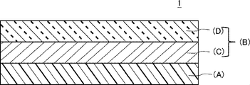
- FIG. 1 is a schematic cross-sectional view showing an example of an electromagnetic wave shield sheet according to this embodiment
- FIG. 1 is a schematic cross-sectional view showing an example of a main part of a shielding wiring board according to this embodiment
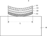
- FIG. 4 is a schematic cross-sectional view for explaining a curl evaluation method of the electromagnetic wave shield sheet according to the example.
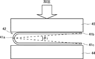
- FIG. 4 is a schematic cross-sectional view for explaining a method for evaluating the deformability of the electromagnetic wave shield sheet according to the example.
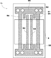
- FIG. 2 is a schematic plan view of the main surface side of the wired circuit board according to the example.
- FIG. 2 is a schematic plan view of the rear surface side of the wired circuit board according to the example.
- FIG. 2 is a schematic plan view of the rear surface side of the shielding wiring board according to the example.
- ⁇ layer laminated on the ⁇ layer means a laminated structure in which the ⁇ layer is directly laminated directly above the ⁇ layer, and the ⁇ layer is laminated on the ⁇ layer via other layers. including stacking configurations that are Numerical values specified in this specification are values obtained by the method disclosed in the examples.
- FIG. 1 shows an example of an electromagnetic wave shield sheet (hereinafter also referred to as "this sheet") according to an embodiment of the present invention.
- the sheet 1 comprises an adhesive layer (A) and a shield layer (B) laminated on the adhesive layer (A).
- the shield layer (B) contains a metal layer (C) laminated on the adhesive layer (A), a binder component (d-1) and a conductive filler (d-2), and the metal layer (C ) and a highly-filled conductive filler layer (D) laminated thereon. Further, no metal layer is formed on the side opposite to the side on which the metal layer (C) of the highly-filled conductive filler layer (D) is formed.
- the content of the conductive filler (d-2) in the highly-filled conductive-filler layer (D) is in the range of 75 to 95% by mass with respect to 100% by mass of the highly-filled conductive-filler layer (D).
- This sheet is bonded to an adherend such as a printed wiring board via the adhesive layer (A), and functions as an electromagnetic wave shielding member for the adherend.
- the shield layer (B) is not composed only of the metal layer (C), but the metal layer and the conductive filler high filling layer (D) containing the binder component (d-1) are used together.
- the shield layer (B) provides excellent electromagnetic wave shielding properties
- the combination of the metal layer (C) and the highly-filled conductive filler layer (D) suppresses curling and burrs, resulting in excellent easy deformation. You can get sex.
- the present shield layer (B) which uses both the metal layer (C) and the conductive filler highly-filled layer (D) containing the binder component (d-1), Since the thickness of the metal layer, which is highly dense and has a problem with gas permeability, can be reduced, the gas permeability can be improved.
- An electromagnetic wave shielding sheet is usually produced and stored in a roll form for reasons such as convenience of transportation and continuous productivity.
- the electromagnetic wave shielding sheet has a metal layer, residual distortion occurs when the sheet is wound into a roll and stored, and curling occurs when the sheet is unwound. Due to this curl, the handleability during cutting and punching is reduced. Moreover, there is a problem that the dimensional accuracy is deteriorated.
- the curling is effectively suppressed by the stress relaxation effect of the binder component (d-1) of the conductive filler highly-filled layer (D) that functions as part of the shield layer (B). be able to.
- the electromagnetic wave shielding sheet wound into a roll may be unwound and punched into a desired size and shape when used.
- a metal layer is formed on the electromagnetic wave shielding sheet, when the conventional electromagnetic wave shielding sheet is punched, burrs are likely to be generated on the edge surface of the sheet.
- This sheet is designed to reduce the thickness of the metal layer, which causes burrs, by using both the metal layer and the highly-filled conductive filler layer containing the binder component (d-1) as the shield layer (B). becomes possible. Further, the stress applied to the sheet during punching can be relieved by the binder component (d-1) of the highly-filled conductive filler layer (D). Therefore, according to the present sheet, it is possible to effectively prevent the generation of burrs.
- a flexible printed wiring board (hereinafter referred to as FPC) to which an electromagnetic wave shield sheet is bonded is sometimes folded and incorporated into an electronic device.
- FPC flexible printed wiring board
- the electromagnetic wave shield sheet includes a metal layer, a repulsive force is generated when the sheet is bent due to its rigidity. Therefore, there is a demand for an electromagnetic wave shielding sheet that is excellent in easily deformable properties.
- a metal layer (C) as a shield layer (B) and a conductive filler highly filled layer (D) containing a binder component (d-1) having a specific content of conductive filler are used in combination.
- the thickness of the metal layer which causes rigidity, can be designed to be thin.
- the shield layer (B) the layer that is placed on the outside when bent and subjected to a higher stress load is the conductive filler high filling layer (D), so that the metal layer (C) is prevented from breaking and cracking. And the appearance defect can be effectively prevented.
- the FPC to which the electromagnetic wave shield sheet is joined requires high-temperature processing such as a solder reflow process.
- the electromagnetic wave shield sheet is required to have permeability to outgas such as water vapor generated from the FPC.
- outgassing may be retained by this metal layer, causing foaming, floating, partial peeling between layers, poor appearance, and the like.
- This sheet is designed to reduce the thickness of the metal layer, which can hinder gas permeability, by using both a metal layer and a highly-filled conductive filler layer containing a binder component (d-1) as the shield layer (B). It becomes possible to By reducing the thickness of the metal layer, gas-permeable micropores are easily formed. Although it is possible to separately provide pores for gas permeation in the metal layer, there is a problem that the number of production steps increases.
- the metal layer (C) of the shield layer (B) is arranged on the side closer to the electronic component (adherend) in which signal wiring and the like are built.
- the highly-filled conductive filler layer (D) has a conductive filler (d-2) dispersed in a binder component (d-1). For this reason, focusing on the portion exhibiting conductivity, the highly-filled conductive-filler layer (D) alone has a certain degree of unevenness on its surface.
- the shield layer (B) of this sheet due to the nature of the current, the current will flow on the surface of the metal layer (C) at high frequencies.
- the transmission characteristics of the signal wiring in the printed circuit board are affected by the current flowing in the nearby conductor. The distance fluctuates and the transmission characteristics become unstable. Therefore, from the viewpoint of transmission characteristics, the shield layer (B) is preferably smooth.
- the electronic component (adherend) side of the shield layer (B) is smooth, and transmission characteristics can be improved.
- the metal layer (C) in the formation of the metal layer (C) by vapor deposition or plating, the metal layer (C) can be formed so as to fill recesses on the surface of the layer (D) filled with a highly conductive filler.
- the metal layer (C) is a metal foil such as a copper foil, it is possible to cover the surface unevenness of the conductive filler highly-filled layer (D) with the smooth metal layer (C).
- the sheet preferably has a repulsive force of 0.01 to 30 mN/cm after the sheet is pressed at 170° C. for 30 minutes. Within this range, the easily deformable property is excellent, and the occurrence of curling and burrs can be more effectively suppressed.
- the method for measuring the repulsive force of the pressed material of this sheet refers to the value obtained by the examples described later. Each layer will be described in detail below.
- the adhesive layer (A) serves to bond the sheet to the adherend. Bonding of the sheet to the adherend is usually performed by thermocompression bonding. The layer after bonding to the adherend is called a bonding layer (A') to distinguish from the adhesive layer (A) of the sheet before bonding to the adherend.
- the adhesive layer (A) can be formed using an adhesive composition.
- the adhesive composition contains a binder component (a-1).
- the binder component (a-1) contains at least a resin.
- resins include thermoplastic resins and thermosetting resins.
- Thermoplastic resin is a resin that softens when heated above the glass transition temperature or melting point
- thermosetting resin is a resin that crosslinks when heated to form a polymer network structure and hardens and does not return to its original state.
- thermoplastic resin When a thermoplastic resin is used as the resin of the binder component (a-1), the thermoplastic resin contained exists in a solid state, and the thermoplastic resin melts during hot pressing with an adherend such as FPC, and after cooling, solid again. A desired adhesive strength can be obtained by making the adhesive strength.
- thermosetting resin when a thermosetting resin is used as the resin of the binder component (a-1), the contained thermosetting resin and curing agent exist in an uncured state (B stage), and the adherend such as FPC and heat press Desired adhesive strength can be obtained by curing (C stage) by such as.
- the binder component (a-1) may be in a semi-cured state in which a part of the binder component (a-1) is cured before joining the adherends.
- the adhesive layer (A) has excellent adhesiveness to the shield layer (B) and has excellent adhesiveness to adherends such as FPC coverlay films (e.g., polyimide resin).
- adherends such as FPC coverlay films (e.g., polyimide resin).
- the binder component (a-1) contains a thermosetting resin and/or a thermoplastic resin containing at least one of hydroxyl group and carboxyl group.
- the binder component (a -1) When applying this sheet to a member that transmits signals such as FCP, in order to reduce the transmission loss of high frequency signals that transmit electronic components such as FPC, the binder component (a -1) was pressed under the conditions of 170° C. for 30 minutes, and the relative dielectric constant at 23° C. and a frequency of 28 GHz was 1.0 to 3.5, and the dielectric loss tangent was 0.0. 0001 to 0.02 is preferable.
- a thermosetting resin is contained as the binder component (a-1)
- the pressed product (a'-1) becomes a cured layer.
- a cured layer is usually formed by treatment at 170° C.
- the heating temperature and/or time are adjusted to form a cured layer, shall be measured.
- curing means not semi-curing as in B stage but complete curing as in C stage.
- dielectric loss is represented by the following formula (1).
- ⁇ in the above equation (1) is the transmission loss of the dielectric
- K is the proportionality constant
- f is the frequency
- ⁇ r is the dielectric constant
- tan ⁇ is the dielectric loss tangent.
- the adhesive layer (A) containing the shield layer (B) in the present sheet and the binder component (a-1) from which the press-treated product (a'-1) having the specific dielectric constant and dielectric loss tangent within the above-described specific ranges is obtained.
- the transmission loss can be reduced more effectively.
- the transmission characteristics of this frequency band can also be effectively reduced.
- a more preferable upper limit of the dielectric constant is 3.0, and a further preferable upper limit is 2.5.
- a more preferable upper limit value of the dielectric loss tangent is 0.01, and a more preferable upper limit value is 0.005.
- the bonding layer (A') of the sheet after bonding to the adherend may be either insulating or conductive.
- the adhesive composition forming the adhesive layer (A) may further contain a conductive filler (a-2).
- a-2 conductive filler
- the bonding layer (A') may be isotropic conductive or anisotropic conductive.
- the isotropic conductivity means that the bonding layer (A′) has conductivity in both the thickness direction and the surface direction
- the anisotropic conductivity means that the bonding layer (A′) is substantially In general, it means having conductivity only in the thickness direction.
- Anisotropic conductivity is preferable from the viewpoint of improving transmission characteristics in a high frequency band and from the viewpoint of cost reduction.
- the binder component (a -1) when the conductive filler (a-2) is contained in the adhesive layer (A), the values of the dielectric constant and the dielectric loss tangent are larger than before the conductive filler is contained, but the binder component (a -1)
- the pressed product (a'-1) at 23 ° C. and a frequency of 28 GHz has a relative permittivity of 1.0 to 3.5 and a dielectric loss tangent of 0.0001 to 0.02, so that the conductive filler Excellent transmission characteristics are obtained even when (a-2) is added.
- This is done by controlling the dielectric properties of the press-treated product (a'-1) of the binder component (a-1) of the adhesive layer (A), and adding the conductive filler (a-2) for shielding. This is believed to be due to the synergistic effect of the effect of increasing the properties and the low dielectric effect of the binder component (a-1).
- the thickness of the adhesive layer (A) is not particularly limited, and can be appropriately designed according to the application. From the viewpoint of thinning, the thickness of the adhesive layer (A) is preferably about 4 to 10 ⁇ m.
- the binder component (a-1) contains a thermosetting resin and a curing agent, and the bonding layer (A') of the sheet after bonding to the adherend is used as a cured layer.
- the bonding layer (A) will be described in detail below.
- thermoplastic resins include polyolefin resins, vinyl resins, acrylic resins, styrene/acrylic resins, diene resins, terpene resins, petroleum resins, cellulose resins, polyamide resins, polyurethane resins, polyester resins, and polycarbonates. Resins, polyimide resins, fluorine resins, and the like can be mentioned. From the viewpoint of transmission loss, a material that satisfies the aforementioned dielectric constant and dielectric loss tangent is preferred, and from the viewpoint of characteristic impedance, a material that satisfies the aforementioned dielectric constant is preferred. Suitable examples include fluorine-based resins. Suitable examples include those classified as liquid crystal polymers.
- the thermoplastic resin can be used alone or in combination of two or more.
- thermosetting functional groups contained in the thermosetting resin include hydroxyl groups, phenolic hydroxyl groups, acid anhydride groups, methoxymethyl groups, carboxyl groups, amino groups, epoxy groups, oxetanyl groups, oxazoline groups, oxazine groups, An aziridine group, a thiol group, an isocyanate group, a blocked isocyanate group, a blocked carboxyl group, and a silanol group.
- Thermosetting resins include, for example, acrylic resins, maleic acid resins, polyolefin resins, polybutadiene resins, polyester resins, polyurethane resins, polyurethane urea resins, polycarbonate resins, epoxy resins, oxetane resins, phenoxy resins, polyimide resins, and polyamide resins. , polyamideimide resins, phenolic resins, alkyd resins, amino resins, polylactic acid resins, oxazoline resins, benzoxazine resins, polyimide benzoxazole resins, polybenzoxazole resins, silicone resins, and fluorine resins.
- Thermosetting resins can be used alone or in combination of two or more.
- the curing agent is not particularly limited as long as it has two or more functional groups capable of reacting with the functional groups of the thermosetting resin.
- Examples of curing agents include epoxy compounds, acid anhydride group-containing compounds, isocyanate compounds, aziridine compounds, amine compounds, phenol compounds, organometallic compounds (metal chelate compounds), polyol compounds, melamine compounds, silane compounds, and carbodiimide compounds. , phenol compounds, benzoxazine compounds, maleimide compounds, and ⁇ -hydroxyalkylamide group-containing compounds.
- Curing agents can be used alone or in combination of two or more.
- the curing agent may be either a low-molecular compound or a high-molecular compound. When a polymer compound is used as the curing agent, the thermosetting resin is used as the component with a large amount, and the curing agent is used as the component with a small amount.
- the curing agent is preferably an isocyanate compound, an epoxy compound, an aziridine compound, a carbodiimide compound, or an organometallic compound.
- the curing agent is preferably an isocyanate compound, an epoxy compound, an aziridine compound, a carbodiimide compound, or an organometallic compound.
- the curing agent is preferably an epoxy compound or an organometallic compound.
- Examples of preferred combinations when two or more curing agents are used in combination include an epoxy compound and an organometallic compound, and an epoxy compound, an aziridine compound, and an organometallic compound. By using them in combination, the crosslinking density can be increased, and the protrusion of the adhesive layer (A) to the outside of the layer and the heat resistance can be effectively improved during thermocompression bonding.
- the isocyanate compounds include, for example, tolylene diisocyanate, hexamethylene diisocyanate, isophorone diisocyanate, xylylene diisocyanate, hydrogenated xylylene diisocyanate, diphenylmethane diisocyanate, hydrogenated diphenylmethane diisocyanate, tetramethylxylylene diisocyanate, naphthalene diisocyanate, triphenylmethane triisocyanate, Polyisocyanate compounds such as polymethylene polyphenyl isocyanate, adducts of these polyisocyanate compounds and polyol compounds such as trimethylolpropane, burettes and isocyanurates of these polyisocyanate compounds, and further these polyisocyanate compounds and known poly Examples include adducts with ether polyols, polyester polyols, acrylic polyols, polybutadiene polyols, polyisoprene poly
- epoxy compound examples include ethylene glycol diglycidyl ether, polyethylene glycol diglycidyl ether, 1,6-hexanediol diglycidyl ether, bisphenol A/epichlorohydrin type epoxy resin, N,N,N',N'- tetraglycidyl-m-xylylenediamine, 1,3-bis(N,N-diglycidylaminomethyl)cyclohexane, N,N-diglycidylaniline, N,N-diglycidyltoluidine and the like.
- polycarbodiimide examples include the Carbodilite series manufactured by Nisshinbo. Among them, Carbodilite V-01, 03, 05, 07 and 09 are preferable because of their excellent compatibility with organic solvents.
- aziridine compound examples include 2,2'-bishydroxymethylbutanol tris[3-(1-aziridinyl)propionate], 4,4'-bis(ethyleneiminocarbonylamino)diphenylmethane, and the like.
- the organometallic compound is a compound composed of a metal and an organic substance, and reacts with the functional groups of the thermosetting resin to form crosslinks.
- the type of organometallic compound is not particularly limited, examples thereof include organoaluminum compounds, organotitanium compounds, and organozirconium compounds.
- the bond between the metal and the organic substance may be a metal-oxygen bond, and is not limited to a metal-carbon bond.
- the binding mode between the metal and the organic substance may be any of chemical bond, coordinate bond, and ionic bond.
- the organoaluminum compound is preferably an aluminum chelate compound.
- Aluminum chelate compounds are, for example, ethylacetoacetate aluminum diisopropylate, aluminum tris(ethylacetoacetate), alkylacetoacetate aluminum diisopropylate, aluminum monoacetylacetonate bis(ethylacetoacetate), aluminum tris(acetylacetate), Aluminum monoacetylacetate bis(ethylacetoacetate), aluminum di-n-butoxide monomethylacetoacetate, aluminum diisobutoxide monomethylacetoacetate, aluminum di-sec-butoxide monomethylacetoacetate, aluminum isopropylate, monosec-butoxyaluminum diisopropylate rate, aluminum-sec-butyrate, aluminum ethylate, and the like.
- Titanium chelate compounds include, for example, titanium acetylacetonate, titanium tetraacetylacetonate, titanium ethylacetoacetate, titanium octylene glycolate, titanium ethylacetoacetate, titanium-1,3-propanedioxybis(ethylacetoacetate), Polytitanium acetyl acetylacetonate, tetraisopropyl titanate, tetra-n-butyl titanate, butyl titanate dimer, tetraoctyl titanate, d'amyl titanate, tetra-tert-butyl titanate, tetrastearyl titanate, titanium isostearate, tri-n-butoxytitanium monostearate, di-i-propoxytitanium distearate, titanium stearate, di-i-propoxytitanium diisostearate,
- the organic zirconium compound is preferably a zirconium chelate compound.
- Zirconium chelate compounds include, for example, zirconium tetraacetylacetonate, zirconium tributoxyacetylacetonate, zirconium monobutoxyacetylacetonate bis(ethylacetoacetate), zirconium dibutoxybis(ethylacetoacetate), zirconium tetraacetylacetonate, normal Propyl zirconate, normal butyl zirconate, zirconium stearate, zirconium octylate and the like.
- organic titanium compounds are preferable from the viewpoint of thermosetting reactivity and heat resistance after curing.
- the content of the curing agent can be appropriately designed, but it is preferable to include 1 to 50 parts by mass with respect to 100 parts by mass of the thermosetting resin. By setting it as this range, crosslink density can be made suitable and hygroscopicity and adhesiveness can be kept favorable. In addition, the elastic modulus of the cured product can be properly maintained.
- the curing agent is more preferably contained in 3 to 40 parts by mass, more preferably 3 to 30 parts by mass, based on 100 parts by mass of the thermosetting resin.
- the binder component (a-1) is subjected to pressing at 170 ° C. for 30 minutes. It is preferable that the substance (a'-1) has the above-described relative permittivity and dielectric loss tangent.
- Suitable examples of the binder component (a-1) include a combination of a thermosetting resin having a carboxyl group and a curing agent containing an epoxy compound and an organometallic compound, a thermosetting resin having a phenolic hydroxyl group, and a polyisocyanate.
- thermosetting resin contains a carboxyl group-containing resin, contains an epoxy compound as a curing agent, and further contains at least one of an organometallic compound and an isocyanate compound.
- the epoxy compound is blended in an epoxy equivalent of preferably 0.5 to 10 times, more preferably 1 to 5 times the equivalent of carboxylic acid.
- the total curing agent equivalent of the organometallic compound and the isocyanate compound is preferably 0.1 to 5 times, more preferably 0.5 to 3 times, the equivalent of the carboxylic acid.
- the reactive functional group value (acid value) of the resin in the binder component (a-1) is preferably 20 mgKOH/g or less, more preferably 10 mgKOH/g or less.
- the lower limit of the reactive functional group value (acid value) is preferably 1 mgKOH/g from the viewpoint of forming a strong crosslinked structure by reacting with many curing agents during curing.
- the conductive filler (a-2) has a function of imparting conductivity to the bonding layer (A').
- the adhesive layer (A) of the present sheet is conductive.
- the conductive filler (a-2) include metal powders such as gold, platinum, silver, copper, nickel, aluminum, tin, palladium, chromium, titanium, zinc, manganese, and indium, alloy powders, and low melting point metals such as solder. Powder can be exemplified.
- Composite fine particles having a coating layer covering the surface of the core are also suitable. Examples thereof include silver-plated copper powder, metal-plated glass fiber and carbon filler.
- Fine particles of conductive polymers such as polyaniline and polyacetylene may also be used.
- highly conductive silver powder, silver-plated copper powder, and low-melting-point metal powder such as solder are preferred.
- the conductive filler can be used singly or in combination of two or more.
- the shape of the conductive filler (a-2) is not limited as long as the desired conductivity is obtained in the bonding layer (A'). Examples thereof include spherical, flake (including leaf-like particles described later), dendrite, plate, needle, rod, and grape. Two or more types of conductive fillers (a-2) having different shapes may be mixed. In order to develop anisotropic conductivity, it is preferably spherical or dendritic. Moreover, from the viewpoint of improving outgas permeability, dendrite-like particles and spherical particles are preferable to flake-like particles. When dendritic particles are used as the conductive filler (a-2), the number of contact points between the conductive fillers increases, and ground connectivity can be further enhanced when this sheet is bonded to an FPC or the like. Details will be described later.
- the average particle size of the conductive filler (a-2) is preferably 2 ⁇ m or more, more preferably 5 ⁇ m or more, and even more preferably 7 ⁇ m or more, from the viewpoint of sufficiently ensuring conductivity.
- the thickness is preferably 30 ⁇ m or less, more preferably 20 ⁇ m or less, and even more preferably 15 ⁇ m or less.
- the average particle size can be determined by a laser diffraction/scattering method particle size distribution analyzer or the like.
- the average particle diameter is the D50 average particle diameter
- the D50 average particle diameter is measured using a laser diffraction/scattering method particle size distribution measuring device LS13320 (manufactured by Beckman Coulter), with a tornado dry powder sample module, It is a numerical value obtained by measuring the conductive filler (a-2), and is the particle diameter at which the cumulative value in the particle diameter cumulative distribution is 50%. Also, the refractive index was set to 1.6.
- the content of the conductive filler (a-2) can be appropriately designed, but it is preferably 45% by mass or less, more preferably 15 to 40% by mass, with respect to 100% by mass of the adhesive layer (A). ⁇ 30% by mass is more preferred. By setting the content to 45% by mass or less, outgas permeability and transmission characteristics can be improved. Further, by setting the amount to 15% by mass or more, the ground connectivity can be further enhanced when the present sheet is bonded to a wiring circuit board such as FPC. Details will be described later.
- a solvent can be appropriately used in the adhesive composition used for forming the adhesive layer (A).
- optional components such as silane coupling agents, curing aids, rust preventives, reducing agents, antioxidants, pigments, dyes, tackifying resins, plasticizers can be used for the purpose of improving desired physical properties and imparting functions. agents, ultraviolet absorbers, antifoaming agents, leveling adjusters, fillers, flame retardants, and the like.
- the shield layer (B) plays a role of preventing malfunction due to external magnetic fields and radio waves and/or reducing unnecessary radiation from electric signals.
- the shield layer (B) contains the metal layer (C) laminated on the adhesive layer (A), the binder component (d-1) and the conductive filler (d-2). and a conductive filler highly-filled layer (D) laminated on the metal layer (C).
- the shield layer (B) may be laminated with a layer other than the metal layer (C) and the highly conductive filler-filled layer (D) within the scope of the present invention.
- both the present sheet before bonding to the adherend and the present sheet after bonding to the adherend are referred to as the shield layer (B).
- the metal layer (C) functions as part of the shield layer (B).
- the metal species constituting the metal layer (C) is not limited within the scope of the present invention, but examples include gold, platinum, silver, copper, nickel, aluminum, tin, palladium, chromium, titanium, zinc, manganese. , and indium.
- a single conductive metal may be used, or an alloy of multiple metals may be used.
- gold, platinum, silver, and copper are preferred, and silver and copper are particularly preferred, from the viewpoint of obtaining superior shielding properties with a thin layer.
- copper, silver and aluminum are more preferable, and copper is even more preferable.
- Suitable examples of copper include rolled copper foil, electrolytic copper foil, evaporated film, and sputtered film.
- electrolytic copper foil is more preferable because the metal layer (C) can be made thinner.
- the metal layer (C) may be a single layer or multiple layers.
- the thickness of the metal layer (C) can be appropriately designed according to the application. 2 ⁇ m is preferred, 0.1 to 1.5 ⁇ m is more preferred, and 0.2 to 1 ⁇ m is even more preferred.
- the micropores have the advantage of remarkably reducing electromagnetic wave noise leakage and exhibiting gas permeability.
- the metal layer (C) obtained by vacuum vapor deposition can easily form micropores, so that gas permeability can be improved.
- the surface roughness of the metal layer (C) can be designed as appropriate. It is preferable that the root-mean-square slope Sdq determined by the following formula based on ISO 25178-2:2012 is 0.0001 to 0.5.
- A is the area of the defined surface
- ⁇ x is the x-axis direction
- ⁇ y is the y-axis direction
- ⁇ z(x, y) is the z-axis direction.
- the root-mean-square slope Sdq can be calculated by processing the coordinate data of the surface profile obtained with either an optical microscope, a laser microscope, or an electron microscope, using analysis software.
- the root-mean-square slope Sdq represents the root-mean-square slope of all points on the defined surface, and is a parameter that expresses the steepness of the unevenness on the defined surface.
- the value of the root-mean-square slope Sdq of the metal layer (C) basically does not change before and after bonding to the adherend by hot pressing or the like. Therefore, the preferred range of the root-mean-square slope Sdq of the interface of the metal layer (C) in contact with the bonding layer (A') after bonding to the adherend is also 0.0001 to 0.5.
- the metal layer (C) may have a plurality of pores penetrating in the thickness direction. Having pores can significantly improve solder reflow resistance and gas permeability.
- the aperture ratio of the pores is preferably 0.10 to 20% from the viewpoint of achieving both solder reflow resistance and high-frequency shielding at a high level.
- the highly-filled conductive-filler layer (D) is a layer that functions as part of the shield layer (B) and contains a binder component (d-1) and a conductive filler (d-2).
- the content of the conductive filler (d-2) is 75 to 95% by mass with respect to 100% by mass of the highly-filled conductive-filler layer (D). By setting it within this range, it is possible to effectively bring out the stress relaxation effect while maintaining good shielding characteristics.
- a more preferred range is 80 to 92.5% by mass, an even more preferred range is 84 to 90% by mass, and a particularly preferred range is 85 to 90% by mass.
- the film thickness of the conductive filler highly-filled layer (D) is not particularly limited, it is preferably 2 to 8 ⁇ m from the viewpoint of thinning. Each component will be described in detail below.
- Binder component (d-1) contains a resin.
- resins include thermoplastic resins and thermosetting resins.
- the thermosetting resin may be a self-crosslinking resin that cures by itself, but is preferably used in combination with a curing agent.
- Suitable examples of the thermoplastic resin, thermosetting resin and curing agent include the compounds exemplified for the binder component (a-1). Thermoplastic resins and thermosetting resins may be used either alone or in combination.
- this binder component (d-1) is used as the binder component (d-1) of the conductive filler highly-filled layer (D) of the present sheet.
- the pressed product (d'-1) obtained by pressing under the conditions of 170 ° C. x 30 minutes has a relative dielectric constant of 1.0 to 3.5 at 23 ° C. and a frequency of 28 GHz, and a dielectric loss tangent of 0.0001 to 0.0001. 0.02 is preferred.
- a more preferable upper limit of the dielectric constant is 3.0, and a further preferable upper limit is 2.5.
- a more preferable upper limit value of the dielectric loss tangent is 0.01, and a more preferable upper limit value is 0.005.
- the pressed product (d'-1) becomes a cured layer.
- the loss tangent peak in the range of 0 to 300 ° C. of the sheet-shaped press-treated product (d'-1) obtained by pressing the binder component (d-1) at 170 ° C. for 30 minutes is 0.1 or more. It is preferable from the viewpoint of improving punching workability.
- the loss tangent peak in the range of 0 to 300° C. is 0.1 or more, the stress during punching can be sufficiently absorbed and relieved, so that the punching workability can be improved.
- the loss tangent peak of the sheet-like pressed product (d'-1) in the range of 0 to 300°C is more preferably 0.3 or more.
- the rubber-like plateau E' rub of the sheet-like press-treated product (d'-1) obtained by pressing the binder component (d-1) at 170° C. for 30 minutes is 1.0 ⁇ 10 4 to 1.0 ⁇ . It is preferably within the range of 10 8 Pa from the viewpoint of improving easy deformability.
- the rubber-like plateau E′ rub of the sheet-like pressed product (d′-1) is within the above range, excellent mechanical strength can be imparted to the highly-filled conductive filler layer (D), and the present sheet It is possible to suppress damage when deforming.
- the rubber-like plateau E' rub of the sheet-like pressed product (d'-1) is more preferably 1.0 ⁇ 10 5 to 1.0 ⁇ 10 8 Pa.
- the rubber-like plateau E' rub of the sheet-shaped pressed product (d'-1) is defined as the average value of the storage elastic modulus of the sheet-shaped pressed product (d'-1) at 150 to 200 ° C. be done.
- the storage elastic modulus of the sheet-like pressed product (d'-1) at each temperature can be determined using a dynamic viscoelasticity measuring device or the like.
- the conductive filler high filling layer (D) having the specific dielectric constant and dielectric loss tangent in the specific range is compared to the case of using the adhesive layer (A) having the specific dielectric constant and dielectric loss tangent in the specific range, FPC etc. Since the distance from the signal wiring of the printed circuit board is far, the effect is small, but the effect of reducing the transmission loss can be obtained. From the viewpoint of more effective reduction in transmission loss reduction, the binder component (a-1) and the binder component (d-1) pressed products (a'-1) and (d'-1) at 23 ° C. , and a dielectric constant of 1.0 to 3.5 and a dielectric loss tangent of 0.0001 to 0.02 at a frequency of 28 GHz.
- a suitable content of the curing agent with respect to 100 parts by mass of the thermosetting resin can be designed as appropriate, but it is preferable to include 1 to 50 parts by mass. By setting it as this range, crosslink density can be made suitable and hygroscopicity and adhesiveness can be kept favorable. In addition, the elastic modulus of the cured product can be properly maintained, and the folding endurance can be improved.
- the curing agent is more preferably contained in 3 to 40 parts by mass, more preferably 3 to 30 parts by mass, based on 100 parts by mass of the thermosetting resin.
- the binder component (d-1) may contain a thermosetting resin and a curing agent, and the conductive filler highly-filled layer (D) after bonding the present sheet to the adherend may be used as the cured layer. preferable.
- the conductive filler (d-2) is preferably metal particles from the viewpoint of maintaining good shielding properties.
- composite fine particles may be used which have a core made of metal or resin and a coating layer in which the surface of the core is coated with a metal.
- metal particles include gold, platinum, silver, copper, nickel, aluminum, tin, palladium, chromium, titanium, zinc, manganese, and indium.
- metals selected from gold, platinum, silver, copper, nickel, aluminum, tin, palladium, chromium, titanium, and zinc are preferable from the viewpoint of maintaining good shielding properties.
- the metal particles may be of a single type, a mixture of multiple types, or may be an alloy. Moreover, it may be the same as or different from the metal species used in the metal layer (C).
- the shape of the conductive filler (d-2) is not limited as long as the conductive filler highly-filled layer (D) has electromagnetic shielding properties such as shielding properties and is easily deformable. Examples include spherical, flake, dendrite, plate, acicular, rod, and grape shapes. Two or more types of conductive fillers (a-2) having different shapes may be mixed. Suitable examples include flake particles. The flake-like particles also include leaf-like particles (for example, particles obtained by flattening dendrite-like particles) having a plurality of notches in the outer edge.
- the aspect ratio of the flake particles is not limited, the aspect ratio ([average length ( ⁇ m)]/[average thickness ( ⁇ m)]) is preferably in the range of 1.1 to 500.
- a solvent can be used as appropriate for the conductive filler-containing composition used for forming the conductive filler highly-filled layer (D).
- optional components such as silane coupling agents, curing aids, rust preventives, reducing agents, antioxidants, pigments, dyes, tackifying resins, plasticizers can be used for the purpose of improving desired physical properties and imparting functions. agents, ultraviolet absorbers, antifoaming agents, leveling adjusters, fillers, flame retardants, and the like.
- This sheet may further laminate a protective layer (E) on the shield layer (B).
- the protective layer (E) has a function of protecting the shield layer (B) and the adhesive layer (A) and a function of preventing the shield layer (B) from being electrically connected to the external conductor.
- the protective layer (E) can be formed using a resin composition.
- the resin composition contains a resin-containing binder component (e-1). Suitable examples of resins include thermoplastic resins and thermosetting resins.
- the thermosetting resin may be a self-crosslinking resin that cures by itself, but is preferably used in combination with a curing agent. Thermoplastic resins and thermosetting resins may be used either alone or in combination. In this specification, both before and after bonding to an adherend are referred to as a protective layer (E).
- the breaking strength of the sheet-like press-treated material (e'-1) obtained by pressing the binder component (e-1) of the protective layer (E) under the conditions of 170° C. for 30 minutes is 15 MPa or more from the viewpoint of improving punching workability. preferably. More preferably, it is 17 MPa or more, and even more preferably 20 MPa or more. Although the upper limit of the breaking strength is not limited, it is usually 50 MPa or less.
- the breaking elongation of the sheet-like press-treated product (e'-1) obtained by pressing the binder component (e-1) of the protective layer (E) at 170° C. for 30 minutes is 80% or more from the viewpoint of punching workability. It is preferable to More preferably, it is 150% or more, and even more preferably 200% or more. Although the upper limit of the breaking elongation is not limited, it is usually 5000% or less.
- the loss tangent peak in the range of 0 to 300° C. of the sheet-shaped press-treated product (e′-1) obtained by pressing the binder component (e-1) of the protective layer (E) at 170° C. for 30 minutes was 0.5. It is preferably 1 or more from the viewpoint of improving punching workability.
- the loss tangent peak in the range of 0 to 300° C. is 0.1 or more, the stress during punching can be sufficiently absorbed and relieved, so that the punching workability can be improved.
- the loss tangent peak of the sheet-like pressed product (e'-1) in the range of 0 to 300°C is more preferably 0.3 or more.
- the loss tangent of the sheet-like pressed product (e'-1) can be obtained by the following formula (3), plot the loss tangent at each temperature in the range of 0 to 300 ° C., and the loss tangent at the maximum point. Peak the value.
- the content of the curing agent can be appropriately designed, but it is preferable to include 1 to 50 parts by mass with respect to 100 parts by mass of the thermosetting resin. By setting it as this range, crosslink density can be made suitable and hygroscopicity and adhesiveness can be kept favorable. In addition, the elastic modulus of the cured product can be properly maintained, and the punching workability can be improved.
- the curing agent is more preferably contained in 3 to 40 parts by mass, more preferably 3 to 30 parts by mass, based on 100 parts by mass of the thermosetting resin.
- the binder component (e-1) contains a thermosetting resin and a curing agent, and the protective layer (E) after bonding the sheet to the adherend is used as a cured layer.
- a solvent can be used as appropriate for the protective layer (E). It may also contain non-conductive particles as an optional component.
- the non-conductive particles have the function of improving the insulating properties of the protective layer (E), increasing the pressing force of the sheet against an adherend such as FPC during hot pressing, and increasing the connectivity with the ground wiring.
- thermally conductive particles or the like may be used in order to improve heat dissipation.
- non-conductive particles examples include non-conductive ceramics, pigments, dyes, etc. Ceramics are preferred because they have high hardness and can transmit pressure to the metal layer without alleviating the pressure received during hot pressing.
- non-conductive particles non-conductive particles having a volume resistivity of 1.0 ⁇ 10 10 ⁇ cm or more are preferred. When the non-conductive particles have a volume resistivity of 1.0 ⁇ 10 10 ⁇ cm or more, the insulating properties of the protective layer (E) can be further improved.
- the volume resistivity of the substance contained in the non-conductive particles is more preferably 1.0 ⁇ 10 12 ⁇ cm or more, still more preferably 1.0 ⁇ 10 14 ⁇ cm or more.
- Substances having a volume resistivity of 1.0 ⁇ 10 10 ⁇ cm or more include aluminum oxide or aluminum trioxide (alumina), zirconium dioxide (zirconia), silicon dioxide (silica), boron carbide, aluminum nitride, boron nitride, oxide Ceramics such as magnesium (magnesia), titanium oxide, etc., can be mentioned.
- a more preferable substance is zirconium dioxide (ZrO 2 ; volume resistivity: 1.0 ⁇ 10 12 ⁇ cm), and a more preferable substance is silica ( SiO 2 ; volume resistivity 1.0 ⁇ 10 14 ⁇ cm).
- the volume resistivity of the substance contained in the non-conductive particles can be measured according to JIS C2141.
- the shape of the non-conductive particles is not limited, but examples include massive, irregular, substantially spherical, spherical, and truly spherical.
- a pigment may be added to color the protective layer (E) to the extent that it does not interfere with the function of the protective layer (E).
- pigments include carbon black, carbon graphite, carbon nanotubes, and graphene.
- optional components include a silane coupling agent, a rust inhibitor, a reducing agent, an antioxidant, a tackifying resin, a plasticizer, an ultraviolet absorber, an antifoaming agent, a leveling modifier, a filler, A flame retardant or the like can be added.
- the thickness of the protective layer (E) is preferably 2-20 ⁇ m. When the thickness of the protective layer (E) is 2 to 20 ⁇ m, dissolution of the protective layer (E) after exposure to cleaning chemicals and peeling from the metal layer can be suppressed.
- the sheet may further comprise other functional layers.
- other functional layers include layers having functions such as hard coat properties, water vapor barrier properties, oxygen barrier properties, thermal conductivity, low dielectric constant, high dielectric constant, and heat resistance.
- this sheet is generally stored with a peelable sheet attached to both main surfaces of the adhesive layer (A) and the protective layer (E) in order to prevent foreign matter from adhering.
- the release sheet is a sheet obtained by subjecting a base material such as paper or plastic to a known release treatment.
- This sheet includes a step of forming an adhesive layer (A), a step of forming a metal layer (C) that functions as part of the shield layer (B), a binder component (d-1) and a conductive filler ( a step of applying a conductive filler-containing composition containing d-2) to form a conductive filler highly-filled layer (D) functioning as part of the shield layer (B).
- the content of the conductive filler (d-2) is 75 to 95% by mass with respect to 100% by mass of the highly-filled conductive filler layer (D).
- the stacking order of this sheet should be in the order of adhesive layer (A)/metal layer (C)/conductive filler high filling layer (D).
- the order of steps for each layer is arbitrary.
- the lamination method of each layer can be arbitrarily performed by a known method. For example, a conductive filler highly-filled layer (D) is formed on the protective layer (E), a metal layer (C) is formed on the conductive filler highly-filled layer (D), and a peelable sheet is adhered.
- An adhesive layer (A) is prepared, and these are laminated in the order of adhesive layer (A)/metal layer (C)/conductive filler highly filled layer (D)/protective layer (E). can be formed by
- Step of forming adhesive layer (A) An adhesive composition used for forming the adhesive layer (A) is prepared. Specifically, the adhesive composition can be obtained by mixing and stirring the ingredients. For stirring, a known stirring device such as Dispermat and homogenizer can be used. After preparing the adhesive composition, an adhesive layer (A) is formed by a known method. For example, the adhesive layer (A) can be formed by coating an adhesive composition on a release sheet and drying it. Coating methods include, for example, gravure coating, kiss coating, die coating, lip coating, comma coating, blade coating, roll coating, knife coating, spray coating, bar coating, spin coating, and dip coating. method can be exemplified. For the drying step, a known drying device such as a hot air dryer or an infrared heater can be used. Alternatively, a sheet-like adhesive layer (A) may be formed using an extruder such as a T-die.
- Step of forming metal layer (C) For the metal layer (C), for example, a metal foil, a metal deposition film, a metal plating film, or the like can be used. Alternatively, the metal layer (C) can be formed by vacuum deposition, sputtering, CVD, or MO (metal organic). The metal layer (C) may be formed by accumulating one or more conductive fillers. Preferable examples of conductive fillers include flake-like particles, dendrite-like particles, and spherical particles. Conductive fillers can be used singly or in combination of two or more. The metal layer (C) can be exemplified by a method of forming it on the conductive filler highly-filled layer (D).
- a known method can be applied to control the root-mean-square gradient Sdq of the surface of the metal layer (C).
- a method of polishing a metal surface using a buff described in JP-A-2017-13473 a method of polishing a metal surface using a coated abrasive, and a carrier material having a predetermined root-mean-square slope Sdq.
- a method of pressing a film having a predetermined root-mean-square slope Sdq and the metal layer (C) and A method of transferring the unevenness of the surface to the metal layer (C) can be mentioned.
- micropores having gas permeability can be easily formed at the same time as the metal layer (C) is formed without providing a separate pore forming step.
- a separate pore forming step may be provided.
- a conventionally known method can be applied to the pore forming method. Examples include a method of forming a patterned resist layer on the metal layer (C) and forming pores at desired positions, a method of screen-printing an anchoring agent in a predetermined pattern and plating the printed surface of the anchoring agent with metal, and A method described in JP-A-2015-63730 can be mentioned.
- a conductive filler-containing composition used for forming the conductive filler highly-filled layer (D) is prepared.
- a conductive filler-containing composition can be obtained by mixing predetermined amounts of ingredients and stirring the mixture. Stirring can be performed, for example, by the same stirring device as that for the adhesive layer (A).
- a conductive filler highly-filled layer (D) is formed by a known method.
- the conductive filler-rich layer (D) can be formed by applying a conductive filler-containing composition onto a release sheet and drying it.
- Preferred examples of the coating method and drying method are the coating examples described in connection with the adhesive layer (A).
- a resin composition used for forming the protective layer (E) is prepared. Specifically, the resin composition can be obtained by mixing and stirring the ingredients. Stirring can be performed, for example, by the same stirring device as that for the adhesive layer (A).
- a protective layer (E) is formed by a known method.
- the protective layer (E) can be formed by coating the resin composition on a release sheet and drying it. Preferred examples of the coating method and drying method are the coating examples described in connection with the adhesive layer (A). It can also be formed by extruding the resin composition into a sheet using an extruder such as a T-die.
- the protective layer (E) may be a film obtained by molding an insulating resin such as polyester, polycarbonate, polyimide, polyamideimide, polyamide, polyphenylene sulfide, polyetheretherketone, or the like.
- FIG. 2 shows an example of a shielding wiring board according to an embodiment of the present invention.
- the shielding wiring board 20 includes the wiring circuit board 10 and the electromagnetic wave shielding sheet 2 .
- the wired circuit board 10 includes an insulating substrate 11, a circuit pattern 12 formed on the insulating substrate 11, and a cover coat layer 13 formed on the insulating substrate 11 and the circuit pattern 12. .
- the electromagnetic wave shield sheet 2 is bonded to the insulating base material 11 using the adhesive layer (A) of this sheet.
- the electromagnetic wave shield sheet 2 may be attached to the wiring circuit board 10, and the bonding area can be appropriately designed. In the example of FIG. are spliced. In the example of FIG. 2, the electromagnetic wave shielding sheet 2 has a four-layer structure of bonding layer (A')/metal layer (C)/conductive filler highly-filled layer (D)/protective layer (E). Any bonding method may be used, but the bonding is usually performed by thermocompression bonding. A portion of the adhesive layer (A) is filled into the vias 14 provided in the cover coat layer 13 by thermocompression bonding, and is bonded to the exposed surface of the ground wiring 12b.
- a portion of the adhesive layer (A) is filled into the vias 14 provided in the cover coat layer 13 by thermocompression bonding, and is bonded to the exposed surface of the ground wiring 12b.
- the insulating base material 11 functions as a support for the circuit pattern 12 .
- the insulating base material 11 is not particularly limited. Polyester, polycarbonate, polyimide, and polyphenylene sulfide can be exemplified as suitable resins when flexibility is required. Considering the use of printed circuit boards that transmit high-frequency signals, resins with low dielectric constants and dielectric loss tangents are preferred, and among the examples of preferred resins, those classified as liquid crystal polymers are more preferred.
- a liquid crystal polymer refers to a polymer that exhibits liquid crystallinity when heated and melted. Glass epoxy, which is excellent in heat resistance, is suitable for insulating substrates that require rigidity.
- the circuit pattern 12 has a signal wiring 12a and a ground wiring 12b.
- the circuit pattern 12 is formed of a copper layer having a thickness of several ⁇ m to several tens of ⁇ m, for example.
- the signal wiring 12a can be applied to, for example, a single-ended transmission line made up of one signal wiring and a differential transmission line made up of two signal wirings. In the differential transmission line, two signal wirings are used, currents of opposite phases are passed through each other, and the potential difference between the signal wirings is read, so that the influence of electromagnetic noise added to the signal wirings can be reduced. It is preferable to use a differential transmission line for the signal wiring 12a because more stable signal transmission can be realized by combining with .
- the cover coat layer 13 is an insulating material that covers the circuit pattern 12 of the shielding wiring board 20 and protects it from the external environment.
- a known insulating material can be appropriately selected.
- a resin having heat resistance and flexibility, such as polyimide, is suitable. Suitable examples include a polyimide film with a thermosetting adhesive, a thermosetting or ultraviolet-curable solder resist, and a photosensitive coverlay film.
- the thickness of the cover coat layer 13 is usually about 10-100 ⁇ m.
- the opening area of the via 14 is not particularly limited, it is preferably 0.8 mm 2 or less from the viewpoint of miniaturization of the shielding wiring board 20 .
- the lower limit is not particularly limited, it is, for example, 0.008 mm 2 or more.
- the bonding of the sheet to the wiring circuit board 10 is generally performed by hot pressing under conditions of, for example, a temperature of about 150 to 190° C., a pressure of about 1 to 3 MPa, and a time of about 1 to 60 minutes.
- the adhesive layer (A) and the cover coat layer 13 are brought into close contact with each other by hot pressing, and the adhesive layer (A) flows to fill the vias 14 formed in the cover coat layer 13 with bonding layers (A′). is obtained.
- the bonding layer (A') exhibits conductivity, the ground wiring 12b and the electromagnetic wave shield sheet 2 are electrically connected.
- the corresponding layer becomes the cured layer.
- the curing treatment can be exemplified by a method of performing post-curing at about 150 to 190° C. for 30 to 90 minutes after hot pressing.
- electromagnetic wave shield sheets 2 may be provided on both sides of the printed circuit board 10 .
- the electromagnetic wave shield sheet 2 can be used as a ground circuit in addition to the function of shielding electromagnetic waves.
- the electromagnetic wave shielding sheet 2 By using the electromagnetic wave shielding sheet 2 as a ground circuit, it is possible to reduce the area of the ground circuit area of the printed circuit board 10, thereby achieving miniaturization and cost reduction.
- Parts and “%” in the examples represent “mass parts” and “mass%”, respectively, and Mw means weight average molecular weight.
- the compounding amounts in the table are parts by mass.
- the acid value, weight average molecular weight (Mw) and glass transition temperature (Tg) of the resin, and the average particle size of the conductive filler were measured by the following methods.
- Mw weight average molecular weight
- HPC-8020 gel permeation chromatograph
- Tg Glass transition temperature
- the D50 average particle size was measured using a laser diffraction/scattering particle size distribution analyzer LS13320 (manufactured by Beckman Coulter, Inc.). It is a numerical value obtained by measuring the conductive filler with a tornado dry powder sample module, and is the particle diameter at which the cumulative value in the particle diameter cumulative distribution is 50%.
- the refractive index was set to 1.6.
- Conductive filler 1 Composite fine particles (dendritic fine particles coated with 10 parts of silver on 100 parts of copper core) Average particle diameter D 50 : 11.0 ⁇ m (manufactured by Fukuda Metal Foil & Powder Co., Ltd.)
- Conductive filler 2 Composite fine particles (spherical fine particles coated with 10 parts of silver per 100 parts of copper core) Average particle diameter D 50 : 10.0 ⁇ m (manufactured by Fukuda Metal Foil & Powder Co., Ltd.)
- Conductive filler 3 Composite fine particles (flake-like fine particles coated with 10 parts of silver per 100 parts of copper core) Average particle diameter D 50 : 17.0 ⁇ m (manufactured by Fukuda Metal Foil & Powder Co., Ltd.)
- Resin 1 Polyimide resin with an acid value of 6 mgKOH/g, Mw of 54,000, and a Tg of 7°C (manufactured by Toyochem Co., Ltd.)
- Resin 2 Polyurethan
- a shield with a peelable sheet is formed by forming a metal layer (C) by vacuum copper vapor deposition on the exposed surface of the highly-filled conductive filler layer (D) with a peelable sheet.
- Layer (B) was obtained.
- the surface roughness (Sdq) of the metal layer (C) on the adhesive layer (A) side was measured by the following method. That is, measurement data of the exposed surface of the metal layer (C) was obtained using a laser microscope (manufactured by Keyence Corporation, VK-X100).
- the acquired measurement data was imported into analysis software (analysis application "VK-H1XA” equipped with ISO 25178 surface texture measurement module “VK-H1XR", both manufactured by Keyence Corporation), and ISO 25178 surface texture measurement was performed (under the conditions: S-filter; 1 ⁇ m, L-filter; 0.2 mm).
- analysis software analysis application "VK-H1XA” equipped with ISO 25178 surface texture measurement module “VK-H1XR”, both manufactured by Keyence Corporation
- ISO 25178 surface texture measurement was performed (under the conditions: S-filter; 1 ⁇ m, L-filter; 0.2 mm).
- the openings were excluded from the measurement range when performing the ISO 25178 surface texture measurement.
- the peelable sheet is removed from the shield layer (B) with the peelable sheet, and the resin composition obtained using a bar coater is applied to the exposed surface of the highly-filled conductive filler layer (D) to a dry thickness of 5 ⁇ m. It was coated as Then, it was dried in an electric oven at 100° C. for 2 minutes to obtain a protective layer (E).
- a slightly adhesive peelable sheet was attached to the protective layer (E) to obtain an electromagnetic wave shielding sheet of Example 1. The dry thickness was measured by the same method as for the adhesive layer (A).
- Examples 2 to 30, Comparative Examples 1 to 5 As shown in Tables 1 to 3, the same as in Example 1 except that the types of the adhesive layer (A), the metal layer (C), the highly-filled conductive filler layer (D), and the protective layer (E) were changed. Electromagnetic wave shielding sheets of Examples 2 to 30 and Comparative Examples 1 to 5 were obtained respectively.
- the conductive filler content is the content in 100% by mass of each layer.
- Example 6 Same as Example 1, except that the components shown in Table 3 were used, and the adhesive layer (A), the highly-filled conductive filler layer (D), the metal layer (C) and the protective layer (E) were laminated in this order.
- An electromagnetic wave shield sheet according to Comparative Example 6 was obtained by the method of .
- the peelable sheet was peeled off from the obtained binder sheet with the peelable sheet, four sheets were laminated using a vacuum heat laminator, heat-treated at 170 ° C. for 30 minutes, cut into a 50 mm square, and a test piece having a thickness of 100 ⁇ m was obtained. Obtained.
- This test piece is stored in an atmosphere of 23 ° C. relative humidity of 50% for 24 hours or more, and a dielectric constant measuring device manufactured by AET Co., Ltd. is measured by the cavity resonator method at a temperature of 23 ° C. and a measurement frequency of 28 GHz. Permittivity and dielectric loss tangent were obtained.
- the values of relative permittivity ( ⁇ ) and dielectric loss tangent (tan ⁇ ) of the pressed product (d'-1) can also be obtained by the same method.
- loss elastic modulus E'' and storage elastic modulus E' at each temperature were read.
- the average value was calculated from those in the range of 150 to 200° C. and defined as the rubber-like plateau E′ rub .
- the loss tangent at each temperature was calculated by dividing the loss modulus E'' by the storage modulus E', and a loss tangent curve was created. The maximum point of the obtained loss tangent curve was defined as the loss tangent peak.
- the loss tangent peak of the sheet-like press-treated product (e'-1) of the binder component (e-1) of the protective layer (E) was also obtained by the same method.
- the resin and curing agent contained in the binder component (e-1) of the protective layer (E) in each example and comparative example were added, and the disper By stirring for 10 minutes at , a binder component (e-1) was obtained.
- the obtained binder component (e-1) is applied to a release sheet using a bar coater so that the dry thickness is 30 ⁇ m, dried in an electric oven at 100° C. for 2 minutes, and dried at 170° C., 30 min, 2 MPa.
- a sheet-shaped press-treated product (e'-1) for measuring breaking strength and breaking elongation.
- This sheet-like pressed material (e'-1) was cut into a size of 20 mm in width and 60 mm in length to obtain a measurement sample.
- the measurement sample was subjected to a tensile test (test speed 50 mm/min) under conditions of a temperature of 25° C. and a relative humidity of 50% using a small desktop tester EZ-TEST (manufactured by Shimadzu Corporation). From the resulting SS curve (Stress-Strain curve), the breaking strength (N/20 mm) and breaking elongation (%) of the sheet-like pressure-treated product (e'-1) were calculated.
- the repulsive force was evaluated by measuring the stiffness value according to the test conditions described in JPCA-TM002 8.4.2.
- a single-sided CCL (Copper Clad Laminate) having a pattern A (L/S: 1.0/1.0 mm, number of lines: 3 reciprocations (6 lines)) described in JPCA-TM002 8.4.2 was prepared.
- the electromagnetic wave shield sheet was cut into a size of 2 cm in width and 6 cm in length to obtain a sample.
- the peelable sheet on the side of the adhesive layer (A) of the electromagnetic wave shielding sheet of each example and comparative example was peeled off, and the exposed adhesive layer (A) and the above-mentioned single-sided CCL were superimposed and heated at 170° C., 2 MPa, and 30 min. was crimped under the conditions of Next, cut into a width of 1.5 cm and a length of 3 cm, peel off the release sheet on the protective layer (E) side, and measure the stiffness value under the test conditions described in JPCA-TM002 8.4.2. Thus, the repulsive force of the electromagnetic wave shield sheet after bonding to the adherend was obtained.
- the protective layer (E) of the evaluation sample 5 is placed on a horizontal table 60 so that the adhesive layer (A) is on the bottom side, and the curl rate in the length direction (winding direction) of the evaluation sample 5 is evaluated. Specifically, as shown in FIG. 3, the horizontal distance L of the electromagnetic wave shield sheet in the length direction (winding direction) of the evaluation sample 5 was measured. Then, the curl rate was calculated using the following formula (5).
- Curl rate [(100-L)/100] x 100 (%)
- the obtained curl rate was evaluated according to the following criteria. +++: Curling rate less than 10%. Very good. ++: Curling rate of 10% or more and less than 20%. Good. +: Curling rate of 20% or more and less than 30%. Practical. NG: Curling rate of 30% or more. Not practical.
- the laminate 42 is placed on a substrate 44 (made of polypropylene).
- a pair of substantially parallel stainless steel plates (not shown) are arranged as spacers on the substrate 44, and the test piece is placed between these stainless steel plates.
- the distance between the pair of stainless steel plates is 3 mm, and the thickness of the stainless steel plates is 0.15 mm.
- the laminated body 42 is folded into a mountain fold at the bent portion 41a near the center, and the right portion 41c, which is one side (right side in FIG. 4) from the bent portion 41a, is the other side from the bent portion 41a. It is set to face the left portion 41b.
- the outer side of the polyimide film/electromagnetic wave shielding sheet laminate 42 in FIG. 4 at the time of mountain folding is the electromagnetic wave shielding sheet.
- the laminate 42 was pressed with a predetermined pressure (0.1 MPa) from above by the silicon rubber plate 45 for 5 seconds.
- a predetermined pressure 0.1 MPa
- the angle ⁇ i formed by the line connecting the right portion 41c and the bent portion 41a and the line connecting the left portion 41b and the bent portion 41a was measured one minute after the press was released.
- An angle obtained by subtracting ⁇ i from the angle ⁇ between the line connecting 41c and the bent portion 41a and the line connecting the left portion 41b and the bent portion 41a was measured as the return angle and evaluated according to the following evaluation criteria. . +++:
- the return angle is less than 10°, and there is no appearance defect such as cracking at the bent portion. Very good.
- the return angle is 10° or more and less than 30°, and there is no appearance defect such as cracking at the bent portion.
- Good. + The return angle is 30° or more and less than 60°, and there is no appearance defect such as cracking at the bent portion.
- Practical. NG The return angle is 60° or more, or appearance defects such as cracks occur at the bent portion. Not practical.
- Transmission characteristics were evaluated using a printed circuit board having a coplanar circuit with an electromagnetic shielding sheet.
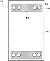
- a schematic plan view of the main surface side of the flexible printed wiring board 15 having a coplanar circuit (hereinafter also referred to as a wiring circuit board having a coplanar circuit) used for measurement is shown in FIG. 5, and a schematic plan view of the back surface side is shown in FIG. show.
- a double-sided CCL “RF775” manufactured by Panasonic Corporation
- Six through holes 52 (diameter 0.1 mm) were provided in the vicinity of the four corners of the rectangular shape.
- a cover coat layer 8 "CISV1215 (manufactured by Nikkan Kogyo Co., Ltd.)" composed of a polyimide film (thickness 12.5 ⁇ m) and an insulating adhesive layer (thickness 15 ⁇ m). pasted.
- the cover coat layer 8 is shown in a perspective view so that the structure of the signal wiring 53 and the like can be understood.
- the copper foil pattern exposed from the cover coat layer 8 was plated with nickel (not shown) and then plated with gold (not shown).
- an electromagnetic wave shielding sheet comprising a laminate of adhesive layer (A)/shield layer (B)/protective layer (E) was prepared, and provided on the adhesive layer (A).
- a release treatment sheet (not shown) was peeled off.
- the electromagnetic wave shielding sheet is pressure-bonded to the entire back surface of the wiring circuit board 15 having the coplanar circuit with the adhesive layer (A) of the electromagnetic wave shielding sheet on the inside under the conditions of 170° C., 2.0 MPa, and 30 minutes.
- a shielding wiring board 21 having a coplanar circuit with an electromagnetic shielding layer having the electromagnetic shielding sheet 6 of each example and comparative example was obtained.
- the back-side ground pattern 56 is shown in a perspective view.
- the L/S (line/space) of the signal wiring 53 was appropriately adjusted so that the characteristic impedance was within ⁇ 10 ⁇ .
- the width of the ground wiring 54 was 100 ⁇ m, and the distance between the ground wiring 54 and the signal wiring 53 was 1 mm.
- the gas permeability was evaluated by contacting a test piece obtained by laminating an electromagnetic shielding sheet on a copper-clad laminate imitating a printed circuit board with molten solder, and evaluating the presence or absence of a change in the appearance of the sample.
- An electromagnetic wave shielding sheet with high gas permeability allows outgassing such as water vapor generated from the wiring circuit board to escape efficiently to the outside of the wiring circuit board, so the appearance does not change. does not escape efficiently, causing foaming and peeling.
- the peelable sheet of the adhesive layer (A) of the electromagnetic wave shield sheet with a width of 25 mm and a length of 70 mm was peeled off, and the exposed adhesive layer (A) and the gold-plated copper-clad laminate (gold-plated) with a total thickness of 64 ⁇ m were removed.
- 0.3 ⁇ m/1 ⁇ m of nickel plating/18 ⁇ m of copper foil/20 ⁇ m of adhesive/25 ⁇ m of polyimide film) were press-bonded to the gold-plated surface under conditions of 170° C., 2.0 MPa, and 30 minutes to obtain a heat-cured laminate.
- the obtained laminate was cut into a size of 10 mm in width and 65 mm in length to prepare a sample. The obtained sample was left in an atmosphere of 40° C.
- Attenuation amount at 15 GHz electromagnetic wave irradiation is -55 dB or more and less than -50 dB.
- NG Attenuation amount at 15 GHz electromagnetic wave irradiation is -45 dB or more. Not practical.
- an electromagnetic shielding sheet that can suppress curling and burrs and has electromagnetic shielding properties, easily deformable properties, and gas permeability.
- This electromagnetic wave shield sheet can be used not only for FPCs, but also for rigid printed wiring boards, COFs, TABs, flexible connectors, liquid crystal displays, touch panels, etc.
- it can be widely used in various applications that require shielding against electromagnetic waves, such as computer cases, building materials such as building walls and window glass, and members that block electromagnetic waves such as vehicles, ships, and aircraft.
- the shielding wiring board of the present invention can be used by being mounted on, for example, electronic devices such as a liquid crystal display, a touch panel, a notebook PC, a mobile phone, a smart phone, a tablet terminal, and the like.
Landscapes
- Engineering & Computer Science (AREA)
- Microelectronics & Electronic Packaging (AREA)
- Physics & Mathematics (AREA)
- Electromagnetism (AREA)
- Shielding Devices Or Components To Electric Or Magnetic Fields (AREA)
- Laminated Bodies (AREA)
- Structure Of Printed Boards (AREA)
Abstract
Description
[1]: 接着剤層(A)と、当該接着剤層(A)の上に積層されたシールド層(B)とを備え、
シールド層(B)は、接着剤層(A)の上に積層された金属層(C)と、バインダー成分(d-1)と導電性フィラー(d-2)を含有し、金属層(C)の上に積層された導電性フィラー高充填層(D)とを有し、当該導電性フィラー高充填層(D)の金属層(C)が形成されている側とは反対側の上には、金属層が形成されておらず、
導電性フィラー高充填層(D)100質量%に対し、導電性フィラー(d-2)の含有率が75~95質量%である電磁波シールドシート。
[2]: 接着剤層(A)は、バインダー成分(a-1)を含み、
当該バインダー成分(a-1)を170℃30分の条件で押圧処理した押圧処理物(a’-1)の比誘電率が23℃、周波数28GHzにおいて1.0~3.5であり、押圧処理物(a’-1)の誘電正接が23℃、周波数28GHzにおいて0.0001~0.02であることを特徴とする[1]記載の電磁波シールドシート。
[3]: 接着剤層(A)は、導電性フィラー(a-2)を含有し、
導電性フィラー高充填層(D)100質量%に対し、導電性フィラー(d-2)の含有率が84~95質量%であり、
接着剤層(A)100質量%に対し、導電性フィラー(a-2)の含有率が15~45質量%であることを特徴とする[1]または[2]記載の電磁波シールドシート。
[4]: シールド層(B)の上に、更に、保護層(E)が積層されており、
保護層(E)は、バインダー成分(e-1)を含み、
当該バインダー成分(e-1)を170℃30分の条件で押圧処理したシート状押圧処理物(e’-1)の破断強度が15MPa以上であることを特徴とする[1]~[3]のいずれかに記載の電磁波シールドシート。
[5]: 170℃30分の条件で押圧処理した後の押圧処理物の反発力が0.01~30mN/cmであることを特徴とする[1]~[4]のいずれかに記載の電磁波シールドシート。
[6]: 絶縁性基材と、前記絶縁性基材上に形成された回路パターンと、前記絶縁性基材および前記回路パターン上に形成されたカバーコート層とを備える配線回路基板と、
電磁波シールドシートとを有し、
前記電磁波シールドシートは、前記カバーコート層上に、請求項1~5のいずれか1項に記載の電磁波シールドシートの接着剤層(A)を用いて接合されたシールド性配線基板。
[7]: [6]記載のシールド性配線基板を備える電子機器。
[8]: 接着剤層(A)とシールド層(B)の積層構成を備える電磁波シールドシートの製造方法であって、
接着剤層(A)を形成する工程と、
シールド層(B)の一部として機能する金属層(C)を形成する工程と、
バインダー成分(d-1)と導電性フィラー(d-2)を含有する導電性フィラー含有組成物を塗工して、シールド層(B)の一部として機能する導電性フィラー高充填層(D)を形成する工程とを有し、
導電性フィラー高充填層(D)100質量%に対し、導電性フィラー(d-2)の含有率を75~95質量%とし、接着剤層(A)、金属層(C)、導電性フィラー高充填層(D)の順に積層し、前記導電性フィラー高充填層(D)の金属層(C)が形成されている側とは反対側の上には、金属層を形成しない、電磁波シールドシートの製造方法。
本発明の実施形態に係る電磁波シールドシート(以下、「本シート」とも記す)の一例を図1に示す。図1に示すように、本シート1は、接着剤層(A)と、この接着剤層(A)の上に積層されたシールド層(B)を備える。シールド層(B)は、接着剤層(A)の上に積層された金属層(C)と、バインダー成分(d-1)と導電性フィラー(d-2)を含有し、金属層(C)の上に積層された導電性フィラー高充填層(D)とを有する。また、導電性フィラー高充填層(D)の金属層(C)が形成されている側とは反対側の上には、金属層が形成されていない。導電性フィラー高充填層(D)中の導電性フィラー(d-2)の含有量は、導電性フィラー高充填層(D)100質量%に対して75~95質量%の範囲とする。本シートは、プリント配線板等の被着体に、接着剤層(A)を介して接合され、被着体の電磁波遮蔽部材として機能する。
一方、本シートによれば、シールド層(B)の一部として機能する導電性フィラー高充填層(D)のバインダー成分(d-1)による応力緩和効果によって、上記カールを効果的に抑制することができる。
本シートは、シールド層(B)として金属層とバインダー成分(d-1)を含む導電性フィラー高充填層を併用することにより、バリの発生の原因となる金属層の厚みを薄く設計することが可能となる。また、打抜き加工時にかかる本シートへの応力を、導電性フィラー高充填層(D)のバインダー成分(d-1)によって緩和させることができる。このため、本シートによれば上記バリの発生を効果的に改善することができる。
本シートは、シールド層(B)として金属層(C)と、導電性フィラーが特定の含有率であるバインダー成分(d-1)を含む導電性フィラー高充填層(D)を併用することにより、剛性の原因となる金属層の厚みを薄く設計することが可能となる。また、シールド層(B)のうち、折り曲げたときに外側に配置される、より応力負荷のかかる層を導電性フィラー高充填層(D)とすることで、金属層(C)の破断、クラックおよび外観不良を効果的に防止できる。
本シートは、シールド層(B)として金属層とバインダー成分(d-1)を含む導電性フィラー高充填層を併用することにより、ガス透過性を阻害する原因となる金属層の厚みを薄く設計することが可能となる。金属層の厚みを薄くすることにより、ガス透過性を有する微小細孔が形成されやすくなる。なお、金属層にガス透過のための細孔を別途設けることも可能であるが、生産工程が増えてしまうという問題がある。
本シートは、優れた易変形性を得る観点からは、本シートを170℃30分の条件で押圧処理した後の押圧処理物の反発力が0.01~30mN/cmであることが好ましい。この範囲とすることにより易変形性に優れ、カールおよびバリの発生をより効果的に抑制することができる。なお、本シートの押圧処理物の反発力の測定方法は、後述する実施例により求められる値をいうものとする。以下、各層について詳述する。
接着剤層(A)は、本シートを被着体に接合する役割を担う。本シートの被着体への接合は、通常、熱圧着により行われる。なお、被着体に接合した後の層を接合層(A’)といい、被着体への接合前の本シートの接着剤層(A)と区別する。
なお、バインダー成分(a-1)として熱硬化性樹脂を含む場合には、押圧処理物(a’-1)は硬化層となる。また、通常、170℃×30分の処理により硬化層となるが、係る条件で硬化層にならないバインダー成分(a-1)に関しては、加熱温度および/または時間を調整して硬化層としてから、測定するものとする。ここでいう硬化とは、Bステージである半硬化でなく、Cステージである完全硬化を意味する。

接着剤層(A)のバインダー成分(a-1)の上記押圧処理物(a’-1)の比誘電率および誘電正接を小さくすることにより、上記式(1)に示すように誘電体損失を低減でき、伝送損失を低減することができる。
熱可塑性樹脂の好適例として、ポリオレフィン系樹脂、ビニル系樹脂、アクリル系樹脂、スチレン・アクリル系樹脂、ジエン系樹脂、テルペン樹脂、石油樹脂、セルロース系樹脂、ポリアミド樹脂、ポリウレタン樹脂、ポリエステル樹脂、ポリカーボネート樹脂、ポリイミド樹脂、フッ素樹脂等が挙げられる。伝送損失の観点から、前述の比誘電率および誘電正接を満たす材料が好ましく、特性インピーダンスの観点から前述の比誘電率を満たす材料が好ましい。好適例としてフッ素系樹脂等が挙げられる。また、液晶ポリマーに分類されるものが好適例として挙げられる。熱可塑性樹脂は、単独または二種類以上併用できる。
熱硬化性樹脂は、例えば、アクリル樹脂、マレイン酸樹脂、ポリオレフィン系樹脂、ポリブタジエン系樹脂、ポリエステル樹脂、ポリウレタン樹脂、ポリウレタンウレア樹脂、ポリカーボネート樹脂、エポキシ樹脂、オキセタン樹脂、フェノキシ樹脂、ポリイミド樹脂、ポリアミド樹脂、ポリアミドイミド樹脂、フェノール系樹脂、アルキド樹脂、アミノ樹脂、ポリ乳酸樹脂、オキサゾリン樹脂、ベンゾオキサジン樹脂、ポリイミドベンズオキサゾール樹脂、ポリベンゾオキサゾール樹脂、シリコーン樹脂、フッ素樹脂が例示できる。熱硬化性樹脂は、単独または二種類以上を併用できる。
有機ジルコニウム化合物はジルコニウムキレート化合物が好ましい。ジルコニウムキレート化合物は、例えば、ジルコニウムテトラアセチルアセトネート、ジルコニウムトリブトキシアセチルアセトネート、ジルコニウムモノブトキシアセチルアセトネートビス(エチルアセトアセテート)、ジルコニウムジブトキシビス(エチルアセトアセテート)、ジルコニウムテトラアセチルアセトネート、ノルマルプロピルジルコネート、ノルマルブチルジルコネート、ステアリン酸ジルコニウム、オクチル酸ジルコニウム等が挙げられる。これらの中でも有機チタン化合物が熱硬化反応性と硬化後の耐熱性の点から好ましい。
これらのうちでも特に、熱硬化性樹脂がカルボキシル基含有樹脂を含み、硬化剤として、エポキシ化合物を含み、更に、有機金属化合物およびイソシアネート化合物の少なくとも一方を含むものが好ましい。エポキシ化合物は、カルボン酸1当量に対して好ましくは0.5~10倍、より好ましくは1~5倍のエポキシ当量を配合する。有機金属化合物およびイソシアネート化合物のトータルの硬化剤当量は、カルボン酸1当量に対して0.1~5倍で配合することが好ましく、0.5~3倍の範囲で配合することがより好ましい。上述したように硬化剤を使用することで、熱硬化後の未反応官能基数を抑制できるため、比誘電率および誘電正接がより低下する。
導電性フィラー(a-2)は、接合層(A’)に導電性を付与する機能を有する。導電性の接合層(A’)とする場合において、本シートの接着剤層(A)の段階での導電性の有無は問わない。導電性フィラー(a-2)としては、金、白金、銀、銅、ニッケル、アルミニウム、錫、パラジウム、クロム、チタン、亜鉛、マンガン、インジウム等の金属粉、合金粉、ハンダ等の低融点金属粉が例示できる。また、核体の表面を被覆した被覆層を有する複合微粒子も好適である。例えば、銀メッキされた銅粉、金属メッキされたガラス繊維やカーボンフィラーなどが挙げられる。また、ポリアニリン、ポリアセチレン等の導電性ポリマーの微粒子を用いてもよい。これらの中でも、導電率の高い銀粉、銀メッキされた銅粉や、ハンダ等の低融点金属粉が好ましい。導電性フィラーは、単独または二種類以上併用できる。
接着剤層(A)の形成に用いる接着剤組成物には、適宜、溶剤を用いることができる。また、上記成分の他、所望の物性向上や機能付与を目的として、任意成分としてシランカップリング剤、硬化助剤、防錆剤、還元剤、酸化防止剤、顔料、染料、粘着付与樹脂、可塑剤、紫外線吸収剤、消泡剤、レベリング調整剤、充填剤、難燃剤などを配合できる。
シールド層(B)は、外部からの磁場や電波による誤動作を防止する役割、または/および電気信号からの不要輻射を低減する役割を担う。シールド層(B)は、前述したように、接着剤層(A)の上に積層されている金属層(C)と、バインダー成分(d-1)と導電性フィラー(d-2)を含有し、金属層(C)の上に積層されている導電性フィラー高充填層(D)とを有する。シールド層(B)は、本発明の趣旨を逸脱しない範囲で、金属層(C)および導電性フィラー高充填層(D)以外の層が積層されていてもよい。なお、本明細書では被着体への接合前の本シート、および被着体への接合後の本シートいずれもシールド層(B)という。金属層(C)および導電性フィラー高充填層(D)も同様とする。
金属層(C)は、シールド層(B)の一部として機能する。金属層(C)を構成する金属種は本発明の趣旨を逸脱しない範囲で限定されないが、一例として、金、白金、銀、銅、ニッケル、アルミニウム、スズ、パラジウム、クロム、チタン、亜鉛、マンガン、インジウムが例示できる。単一の導電性金属を用いても、複数の金属の合金を用いてもよい。より優れたシールド特性を得る観点からは、金、白金、銀、銅、ニッケル、アルミニウム、錫、パラジウム、クロム、チタン、亜鉛から選択される金属を95質量%以上含むことが好ましい。これらのうちでも、薄層でより優れたシールド特性を得る観点からは、金、白金、銀、銅を含むことが好ましく、銀、銅が特に好ましい。

二乗平均平方根傾斜Sdqは、光学顕微鏡、レーザー顕微鏡、および電子顕微鏡いずれかで得られる表面形状の座標データを、解析ソフトによって処理することにより算出することができる。二乗平均平方根傾斜Sdqは、定義表面の全点における傾斜の二乗平均平方根を表しており、定義表面における凹凸の険しさを表現するパラメータである。
導電性フィラー高充填層(D)は、シールド層(B)の一部として機能する層であり、バインダー成分(d-1)と導電性フィラー(d-2)を含有する層である。導電性フィラー(d-2)の含有率は、導電性フィラー高充填層(D)100質量%に対して75~95質量%とする。この範囲とすることにより、シールド特性を良好に保ちつつ、応力緩和効果を効果的に引き出すことができる。より好適な範囲は80~92.5質量%であり、更に好適な範囲は84~90質量%であり、特に好適な範囲は85~90質量%である。
バインダー成分(d-1)は樹脂を含む。樹脂の好適例として、熱可塑性樹脂、熱硬化性樹脂が例示できる。熱硬化性樹脂は、熱硬化性樹脂単独で硬化する自己架橋型の樹脂でもよいが、硬化剤と組合せて用いることが好ましい。熱可塑性樹脂、熱硬化性樹脂および硬化剤のそれぞれの好適例は、バインダー成分(a-1)で例示した化合物が挙げられる。熱可塑性樹脂および熱硬化性樹脂はいずれか単独または両者を併用して用いられる。
導電性フィラー(d-2)は、シールド特性を良好に保つ観点から金属粒子が好適である。また、金属や樹脂を核体とし、核体の表面を金属により被覆した被覆層を有する複合微粒子を用いてもよい。
導電性フィラー高充填層(D)の形成に用いる導電性フィラー含有組成物には、適宜、溶剤を用いることができる。また、上記成分の他、所望の物性向上や機能付与を目的として、任意成分としてシランカップリング剤、硬化助剤、防錆剤、還元剤、酸化防止剤、顔料、染料、粘着付与樹脂、可塑剤、紫外線吸収剤、消泡剤、レベリング調整剤、充填剤、難燃剤などを配合できる。
本シートは、シールド層(B)上に更に保護層(E)を積層してもよい。保護層(E)は、シールド層(B)や接着剤層(A)を保護する機能、およびシールド層(B)が外部導体と電気的に接続することを防止する機能を有する。
数式(3):
(シート状押圧処理物(e’-1)の損失正接)=
(シート状押圧処理物(e’-1)の損失弾性率)/(シート状押圧処理物(e’-1)の貯蔵弾性率)
保護層(E)は、適宜、溶剤を用いることができる。また、任意成分として非導電性粒子を含んでいてもよい。非導電性粒子は保護層(E)の絶縁性を向上させるとともに、熱プレス時に本シートをFPC等の被着体への押し込み力を高め、グランド配線との接続性を高める機能を有する。また、放熱性を高めるために熱伝導性粒子などを用いてもよい。
本シートは、更に、他の機能層を備えていてもよい。他の機能層として、ハードコート性、水蒸気バリア性、酸素バリア性、熱伝導性、低誘電率、高誘電率性または耐熱性等の機能を有する層が例示できる。
以下、本シートの製造方法の一例について説明する。但し、本発明の製造方法は以下の製造方法に限定されるものではない。本シートは、接着剤層(A)を形成する工程と、シールド層(B)の一部として機能する金属層(C)を形成する工程と、バインダー成分(d-1)と導電性フィラー(d-2)を含有する導電性フィラー含有組成物を塗工して、シールド層(B)の一部として機能する導電性フィラー高充填層(D)を形成する工程とを有する。導電性フィラー高充填層(D)100質量%に対し、導電性フィラー(d-2)の含有率が75~95質量%とする。
接着剤層(A)の形成に用いる接着剤組成物を調製する。具体的には、配合成分を混合し、攪拌することにより接着剤組成物を得ることができる。攪拌は、ディスパーマット、ホモジナイザー等の公知の攪拌装置を使用できる。接着剤組成物を調製した後、公知の方法により接着剤層(A)を形成する。例えば、接着剤組成物を剥離性シート上に塗工して乾燥することで接着剤層(A)を形成できる。塗工方法は、例えば、グラビアコート方式、キスコート方式、ダイコート方式、リップコート方式、コンマコート方式、ブレード方式、ロールコート方式、ナイフコート方式、スプレーコート方式、バーコート方式、スピンコート方式、ディップコート方式が例示できる。乾燥工程は、熱風乾燥機、赤外線ヒーター等の公知の乾燥装置を使用できる。また、Tダイのような押出成形機を用いてシート状の接着剤層(A)を形成してもよい。
金属層(C)は、例えば、金属箔、金属蒸着膜、金属メッキ膜等を使用できる。また、真空蒸着、スパッタリング、CVD法、MO(メタルオーガニック)により金属層(C)を形成できる。一種または二種以上の導電性フィラーを集積させることにより金属層(C)を形成してもよい。導電性フィラーの好適例として、フレーク状粒子、デンドライト状粒子、球状粒子が挙げられる。導電性フィラーは一種単独または二種以上を組み合わせて用いることができる。金属層(C)は、導電性フィラー高充填層(D)上に形成する方法が例示できる。
導電性フィラー高充填層(D)の形成に用いる導電性フィラー含有組成物を調製する。具体的には、配合成分を所定量混合し、攪拌することにより導電性フィラー含有組成物を得ることができる。攪拌は、例えば、接着剤層(A)と同様の撹拌装置により行うことができる。導電性フィラー含有組成物を調製した後、公知の方法により導電性フィラー高充填層(D)を形成する。例えば、導電性フィラー含有組成物を剥離性シート上に塗工して乾燥することで導電性フィラー高充填層(D)を形成できる。また、保護層(E)上に塗工して乾燥することで導電性フィラー高充填層(D)を形成してもよい。塗工方法・乾燥方法の好適例として、接着剤層(A)で説明した塗工例が例示できる。
保護層(E)の形成に用いる樹脂組成物を調製する。具体的には、配合成分を混合し、撹拌することにより樹脂組成物を得ることができる。攪拌は、例えば、接着剤層(A)と同様の撹拌装置により行うことができる。樹脂組成物を調製した後、公知の方法により保護層(E)を形成する。例えば、樹脂組成物を剥離性シート上に塗工して乾燥することで保護層(E)を形成できる。塗工方法・乾燥方法の好適例として、接着剤層(A)で説明した塗工例が例示できる。また、Tダイのような押出成形機を使用して樹脂組成物をシート状に押し出すことで形成することもできる。また、保護層(E)は、ポリエステル、ポリカーボネート、ポリイミド、ポリアミドイミド、ポリアミド、ポリフェニレンサルファイド、ポリエーテルエーテルケトン等の絶縁性樹脂を成形したフィルムを使用することもできる。
本発明の実施形態に係るシールド性配線基板の要部の一例を図2に示す。図2に示すように、シールド性配線基板20は、配線回路基板10と電磁波シールドシート2を備える。配線回路基板10は、絶縁性基材11と、この絶縁性基材11上に形成された回路パターン12と、絶縁性基材11および回路パターン12上に形成されたカバーコート層13とを備える。電磁波シールドシート2は、絶縁性基材11に本シートの接着剤層(A)を用いて接合されている。
酸価はJIS K0070に準じて測定した。共栓三角フラスコ中に試料約1gを精密に量り採り、テトラヒドロフラン/エタノール(容量比:テトラヒドロフラン/エタノール=2/1)混合液100mLを加えて溶解する。これに、フェノールフタレイン試液を指示薬として加え、0.1Nアルコール性水酸化カリウム溶液で滴定し、指示薬が淡紅色を30秒間保持した時を終点とした。酸価は次式により求めた(単位:mgKOH/g)。
酸価(mgKOH/g)=(5.611×a×F)/S
ただし、
S:試料の採取量(g)
a:0.1Nアルコール性水酸化カリウム溶液の消費量(mL)
F:0.1Nアルコール性水酸化カリウム溶液の力価
Mwの測定はGPC(ゲルパーミエーションクロマトグラフ)「HPC-8020」(東ソー社製)により行った。GPCは溶媒(THF;テトラヒドロフラン)に溶解した物質をその分子サイズの差によって分離定量する液体クロマトグラフである。本測定は、カラムに「LF-604」(昭和電工社製:迅速分析用GPCカラム:6mmID×150mmサイズ)を直列に2本接続して用い、流量0.6mL/min、カラム温度40℃の条件で行った。Mwの決定はポリスチレン換算で行った。
Tgの測定は、示差走査熱量測定「DSC-1」(メトラー・トレド社製)によって測定した。
D50平均粒子径は、レーザー回折・散乱法粒度分布測定装置LS13320(ベックマン・コールター社製)を使用した。トルネードドライパウダーサンプルモジュールにて、導電性フィラーを測定して得た数値であり、粒子径累積分布における累積値が50%の粒子径である。なお、屈折率の設定は1.6とした。
実施例および比較例に用いた原料を以下に示す。表1~3中の導電性フィラー(a-2)中の1~3のフィラーおよび導電性フィラー(d-2)中の1~3のフィラーは、それぞれ以下の導電性フィラー1~3に対応する。他の樹脂、硬化剤も同様である。
・導電性フィラー1:複合微粒子(核体の銅100部に対して銀が10部被覆されたデンドライト状の微粒子)平均粒径D50:11.0μm(福田金属箔粉工業社製)
・導電性フィラー2:複合微粒子(核体の銅100部に対して銀が10部被覆された球状の微粒子)平均粒径D50:10.0μm(福田金属箔粉工業社製)
・導電性フィラー3:複合微粒子(核体の銅100部に対して銀が10部被覆されたフレーク状の微粒子)平均粒径D50:17.0μm(福田金属箔粉工業社製)
・樹脂1:酸価6mgKOH/g、Mw54,000、Tg7℃のポリイミド樹脂(トーヨーケム社製)
・樹脂2:酸価5mgKOH/g、Mw61,000、Tg-5℃のポリウレタン樹脂(トーヨーケム社製)
・樹脂3:酸価10mgKOH/g、Mw47,000、Tg12℃のポリエステル樹脂(トーヨーケム社製)
・硬化剤1:エポキシ化合物、「JER828」(ビスフェノールA型エポキシ樹脂、エポキシ当量=189g/eq、三菱ケミカル社製)
《接着剤層(A)の作製》
固形分換算で樹脂1を100部、導電性フィラー1を39部、硬化剤1(エポキシ化合物)を15部容器に仕込み、不揮発分濃度が40%になるように混合溶剤(トルエン:イソプロピルアルコール=2:1(質量比))を加えディスパーで10分攪拌して接着剤組成物を得た。
得られた接着剤組成物をバーコーターで乾燥厚みが10μmになるように剥離性シート上に塗工し、100℃の電気オーブンで2分間乾燥することで接着剤層(A)を得た。乾燥厚みはABSデジマチックインジケータID-CX(ミツトヨ社製)にて測定した。
固形分換算で樹脂1を100部、導電性フィラー3を1035部、硬化剤1(エポキシ化合物)を15部容器に仕込み、不揮発分濃度が40%になるように混合溶剤(トルエン:イソプロピルアルコール=2:1(質量比))を加えディスパーで10分攪拌して導電性フィラー含有組成物を得た。
得られた導電性フィラー含有組成物をバーコーターで乾燥厚みが10μmになるように剥離性シート上に塗工し、100℃の電気オーブンで2分間乾燥することで導電性フィラー高充填層(D)を得た。導電性フィラー高充填層(D)の乾燥厚みは接着剤層(A)と同様の方法により測定した。
剥離性シート付きの導電性フィラー高充填層(D)の導電性フィラー高充填層(D)露出面に、真空銅蒸着を施して金属層(C)を形成することにより、剥離性シート付きシールド層(B)を得た。金属層(C)の接着剤層(A)側の表面粗さ(Sdq)は、以下の方法により測定した。即ち、露出した金属層(C)の表面をレーザーマイクロスコープ(キーエンス社製、VK-X100)を使用し、測定データ取得を行った。取得した測定データを解析ソフトウェア(ISO 25178表面性状計測モジュール「VK-H1XR」を備えた、解析アプリケーション「VK-H1XA」、ともにキーエンス社製)に取り込み、ISO25178表面性状計測を実行した(条件は、S‐フィルター;1μm、L‐フィルター;0.2mm)。なお、表面に開口部を有する金属層(C)については、ISO 25178表面性状計測を実行する際には、開口部は計測範囲から除外した。
固形分換算で樹脂1を100部、硬化剤1(エポキシ化合物)15部を加えディスパーで10分攪拌することで樹脂組成物を得た。剥離性シート付きシールド層(B)から剥離性シートを除去し、導電性フィラー高充填層(D)の露出面に、バーコーターを使用して得られた樹脂組成物を乾燥厚みが5μmになるように塗工した。そして、100℃の電気オーブンで2分間乾燥して保護層(E)を得た。次いで、保護層(E)に微粘着剥離性シートを貼り合わせ、実施例1の電磁波シールドシートを得た。乾燥厚みは接着剤層(A)と同様の方法により測定した。
表1~3に示すように、接着剤層(A)、金属層(C)、導電性フィラー高充填層(D)および保護層(E)の種類を変更した以外は、実施例1と同様に行うことで、実施例2~30、比較例1~5の電磁波シールドシートをそれぞれ得た。なお、導電性フィラー含有率は、各層100質量%中の含有率である。
表3に示す成分を用い、更に、接着剤層(A)、導電性フィラー高充填層(D)、金属層(C)および保護層(E)の順に積層した以外は、実施例1と同様の方法により、比較例6に係る電磁波シールドシートを得た。
金属層(C)の厚みは、以下の方法により測定した。
電磁波シールドシートの接着剤層(A)側の剥離性シートを剥がし、露出した接着剤層(A)とポリイミドフィルム(東レ・デュポン社製「カプトン200EN」)を貼り合せ、2MPa、170℃の条件で30分熱プレスした。これを幅5mm、長さ5mm程度の大きさに切断した後、エポキシ樹脂(ペトロポキシ154、マルトー社製)をスライドガラス状に0.05g滴下し、電磁波シールドシートを接着させ、スライドガラス/電磁波シールドシート/ポリイミドフィルムの構成の積層体を得た。得られた積層体をクロスセクションポリッシャー(日本電子社製、SM-09010)を用いてポリイミドフィルム側からイオンビーム照射により切断加工して、熱プレス後の電磁波シールドシートの測定試料を得た。
混合溶剤(トルエン:イソプロピルアルコール=2:1(質量比))に、各実施例および比較例における接着剤層(A)のバインダー成分(a-1)に含有される樹脂および硬化剤を加え、ディスパーで10分攪拌することでバインダー組成物(バインダー成分(a-1))を得た。次いで、バインダー組成物を乾燥厚み25μmになるように剥離性シートに塗工し、100℃の電気オーブンで2分間乾燥して、剥離性シート付きバインダーシートを得た。そして、得られた剥離性シート付きバインダーシートから剥離性シートを剥離し、真空熱ラミネーターを用いて4枚積層し、170℃、30minで加熱処理し、50mm四方に切り出し、厚み100μmの試験片を得た。この試験片を23℃相対湿度50%の雰囲気下で24時間以上保管し、エー・イー・ティー社製の誘電率測定装置を用い、空洞共振器法により測定温度23℃、測定周波数28GHzにおける比誘電率および誘電正接を求めた。なお、押圧処理物(d’-1)の比誘電率(ε)、誘電正接(tanδ)の値も同様の方法により求めることができる。
混合溶剤(トルエン:イソプロピルアルコール=2:1(質量比))に、各実施例および比較例における導電性フィラー高充填層(D)のバインダー成分(d-1)に含有される樹脂および硬化剤を加え、ディスパーで10分攪拌することでバインダー成分(d-1)をそれぞれ得た。得られたバインダー成分(d-1)を、バーコーターを用いて乾燥厚みが30μmになるように剥離性シートに塗工し、100℃の電気オーブンで2分間乾燥し、170℃、30min、2MPaで押圧処理し、その後、剥離性シートを剥がすことにより、破断強度および破断伸度測定用のシート状押圧処理物(d’-1)を得た。このシート状押圧処理物(d’-1)の中心部分を幅5mm・長さ30mmに切出し、試料とした。この試料を、動的粘弾性測定装置(動的粘弾性測定装置DVA-200、アイティー計測制御社製)にセットし、測定温度領域:-30~300℃、昇温速度:10℃/分、測定周波数:1Hz、歪:0.08%の条件にて動的粘弾性測定を行い、各温度での損失弾性率E’’、貯蔵弾性率E’を読み取った。得られた貯蔵弾性率のうち、150~200℃の範囲にあるものから平均値を算出し、ゴム状平坦域E’rubとした。また、損失弾性率E’’を貯蔵弾性率E’で除することで各温度の損失正接を算出し、損失正接曲線を作成した。得られた損失正接曲線の極大点を損失正接ピークとした。
保護層(E)のバインダー成分(e-1)のシート状押圧処理物(e´-1)の損失正接ピークについても同様の方法により求めた。
混合溶剤(トルエン:イソプロピルアルコール=2:1(質量比))に、各実施例および比較例における保護層(E)のバインダー成分(e-1)に含有される樹脂および硬化剤を加え、ディスパーで10分攪拌することでバインダー成分(e-1)を得た。得られたバインダー成分(e-1)を、バーコーターを用いて乾燥厚みが30μmになるように剥離性シートに塗工し、100℃の電気オーブンで2分間乾燥し、170℃、30min、2MPaで押圧処理し、その後、剥離性シートを剥がすことにより、破断強度および破断伸度測定用のシート状押圧処理物(e´-1)を得た。このシート状押圧処理物(e´-1)を幅20mm×長さ60mmの大きさに切断して測定試料とした。測定試料について、小型卓上試験機EZ-TEST(島津製作所社製)を用いて温度25℃、相対湿度50%の条件下で、引っ張り試験(試験速度50mm/min)を実施した。得られたS-S曲線(Stress-Strain曲線)からシート状押圧処理物(e´-1)の破断強度(N/20mm)および破断伸度(%)を算出した。
反発力は、JPCA-TM002 8.4.2に記載の試験条件に準じてスティフネス(stiffness)値を測定して評価した。JPCA-TM002 8.4.2に記載のパターンA(L/S:1.0/1.0mm、ライン数:3往復(六本))の片面CCL(Copper Clad Laminate)を用意した。次いで、電磁波シールドシートを幅2cm・長さ6cmの大きさにカットし、試料とした。各実施例および比較例の電磁波シールドシートの接着剤層(A)側の剥離性シートを剥がし、露出した接着剤層(A)と、前述の片面CCLとを重ね合わせて170℃、2MPa、30minの条件で圧着させた。次いで、幅1.5cm、長さ3cmにカットして保護層(E)側の剥離性シートを剥がし、JPCA-TM002 8.4.2に記載の試験条件にてスティフネス(stiffness)値を測定することにより、被着体に接合した後の電磁波シールドシートの反発力を求めた。
打抜き加工性は、以下に示す方法にて評価した。
実施例、比較例で得られた剥離フィルムのついた電磁波シールドシートを、抜き加工機にて10mmx30mmに総ピース数50個型抜きし、不良品に該当するピースの個数を数えた。以下に示す数式(4)を用いて不良率を算出し、打抜き加工性を評価した。
数式(4):
(不良率)=(不良品に該当するピース数)/(型抜きした総ピース数)×100
なお、不良品とは、型抜きの形に加工された後に、金属層(C)端部でバリ(捲れ)が発生したものを指す。
評価基準は以下の通りとした。
+++:不良率が10%未満。 極めて良好である。
++:不良率が10%以上15%未満 良好である。
+:不良率が15%以上25%未満 実用可。
NG:不良率が25%以上 実用不可。
両面に剥離性シートがついている電磁波シールドシート(長さ1000mm、幅300mm)を準備した。そして、3.0インチABSコア(昭和丸筒社製)に、電磁波シールドシートの長さ方向が巻き方向になるように巻きつけ、300mm長さのロール状試料を得た。このロール状試料の内側は接着剤層(A)、外側は保護層(E)となるようにした。得られたロール状試料を40℃湿度90%RHの条件下に7日間曝露した後、当該剥離性シート付き電磁波シールドシートを巻き戻した。そして、長さ方向500mm地点が中心となるように、また、巻き方向(長さ方向)と幅方向が各辺の方向と一致するように100mm×100mmサイズに裁断し、評価用試料5を得た。その後、評価用試料5の保護層(E)が下側、接着剤層(A)が上側になるように水平な台60に置き、評価用試料5の長さ方向(巻き方向)のカール率を評価した。具体的には、図3に示すように、評価用試料5の長さ方向(巻き方向)の電磁波シールドシートの水平方向の距離Lを測定した。そして、以下の数式(5)を用いてカール率を計算した。
数式(5) カール率=〔(100-L)/100〕×100(%)
得られたカール率を下記の基準で評価した。
+++:カール率10%未満。極めて良好である。
++:カール率10%以上、20%未満。良好である。
+:カール率20%以上、30%未満。実用可。
NG:カール率30%以上。実用不可。
易変形性は図4に示す試験装置を用いて評価した。まず、電磁波シールドシートの接着剤層(A)の剥離性シートを剥離し、接着剤層(A)に、厚さが50μmのポリイミドフィルム(東レ・デュポン社製「カプトン200EN」)を150℃、1MPaおよび30minの条件で圧着し、ポリイミドフィルムに熱圧着させた電磁波シールドシートを得た。その後、縦寸法10mm、横寸法100mmの大きさの試験片(ポリイミドフィルム/電磁波シールドシート)である積層体42を得た。
+++:戻り角10°未満であり、且つ折り曲げ箇所で割れ等の外観不良が無い。極めて良好である。
++:戻り角10°以上、30°未満であり、且つ折り曲げ箇所で割れ等の外観不良が無い。良好である。
+:戻り角30°以上、60°未満であり、且つ折り曲げ箇所で割れ等の外観不良が無い。実用可。
NG:戻り角60°以上、もしくは折り曲げ箇所で割れ等の外観不良が生じる。実用不可。
伝送特性は、電磁波シールドシート付きコプレーナ回路を有する配線回路板を用いて評価した。測定に用いたコプレーナ回路を有するフレキシブルプリント配線板15(以下、コプレーナ回路を有する配線回路基板ともいう)の主面側の模式的平面図を図5、裏面側の模式的平面図を図6に示す。まず、厚さ50μmのポリイミドフィルム50の両面に、厚さ12μmの圧延銅箔を積層した両面CCL「R-F775」(パナソニック社製)を用意した。そして、矩形状の4つのコーナー部近傍に、其々6か所のスルーホール52(直径0.1mm)を設けた。なお、図中においては、図示の便宜上、各コーナー部にスルーホール52を2つのみ示している。次いで、無電解メッキ処理を行った後に、電解メッキ処理を行って10μmの銅メッキ膜51を形成し、スルーホール52内に形成された銅メッキ膜を介して主面-裏面間の導通を確保した。その後、図5に示すように、ポリイミドフィルム50の主面に長さが10cmの2本の信号配線53、およびその外側に信号配線53と並行なグランド配線54、およびグランド配線54から延在され、ポリイミドフィルム50の短手方向のスルーホール52を含む領域にグランドパターン55を形成した。
+++:15GHzにおける伝送損失が7.0dB未満。極めて良好である。
++:15GHzにおける伝送損失が7.0dB以上、7.5dB未満。良好である。
+:15GHzにおける伝送損失が7.5dB以上、8.0dB未満。実用可。
NG:15GHzにおける伝送損失が8.0dB以上。実用不可。
ガス透過性は、配線回路基板を模した銅張積層板に電磁波シールドシートを積層した試験片と、溶融半田とを接触させ、そのサンプルの外観変化の有無により評価した。ガス透過性が高い電磁波シールドシートは、配線回路基板から発生する水蒸気等のアウトガスを効率よく配線回路基板外に逃がすことができるため、外観が変化しないが、ガス透過性が低い電磁波シールドシートではアウトガスが効率よく逃げず、発泡や剥がれが発生する。
まず、幅25mm・長さ70mmの電磁波シールドシートの接着剤層(A)の剥離性シートを剥がし、露出した接着剤層(A)と、総厚64μmの金メッキ処理された銅張積層板(金メッキ0.3μm/ニッケルメッキ1μm/銅箔18μm/接着剤20μm/ポリイミドフィルム25μm)の金メッキ面とを170℃、2.0MPa、30分の条件で圧着し、熱硬化させた積層体を得た。得られた積層体を幅10mm・縦65mmの大きさに切り取り、試料を作製した。得られた試料を40℃、90%RHの雰囲気下で72時間放置した。その後、試料のポリイミドフィルム面を下にして250℃の溶融半田上に1分間浮かべた。そして、取り出した試料の外観を目視で観察し、以下の基準で評価した。
+++:外観変化不良が、目視において認められない。極めて良好である。
++:外観不良の範囲が試料中の保護層(E)面積の10%以下。良好である。
+:外観不良の範囲が試料中の保護層(E)面積の10%より広く、30%以下。実用可。
NG:外観不良の範囲が試料中の保護層(E)面積の30%より広い。
電磁波シールドシートを剥離性フィルムに挟んで2MPaの圧力で170℃×30分間、熱プレス(硬化)し、剥離性フィルムを除いた状態のものを測定サンプルとした。高周波シールド性はASTM D4935に準拠し、キーコム社製の同軸管タイプのシールド効果測定システムを用いて、100MHz~15GHz条件で電磁波の照射を行った。電磁波が電磁波シールドシートで減衰する減衰量を測定し、以下の基準に従って評価した。なお、減衰量の測定値は、デシベル(単位;dB)である。
+++:15GHzの電磁波照射時の減衰量が、-55dB未満。極めて良好である。
++:15GHzの電磁波照射時の減衰量が、-55dB以上、-50dB未満。良好。
+:15GHzの電磁波照射時の減衰量が、-50dB以上、-45dB未満。実用可。
NG:15GHzの電磁波照射時の減衰量が、-45dB以上。実用不可。
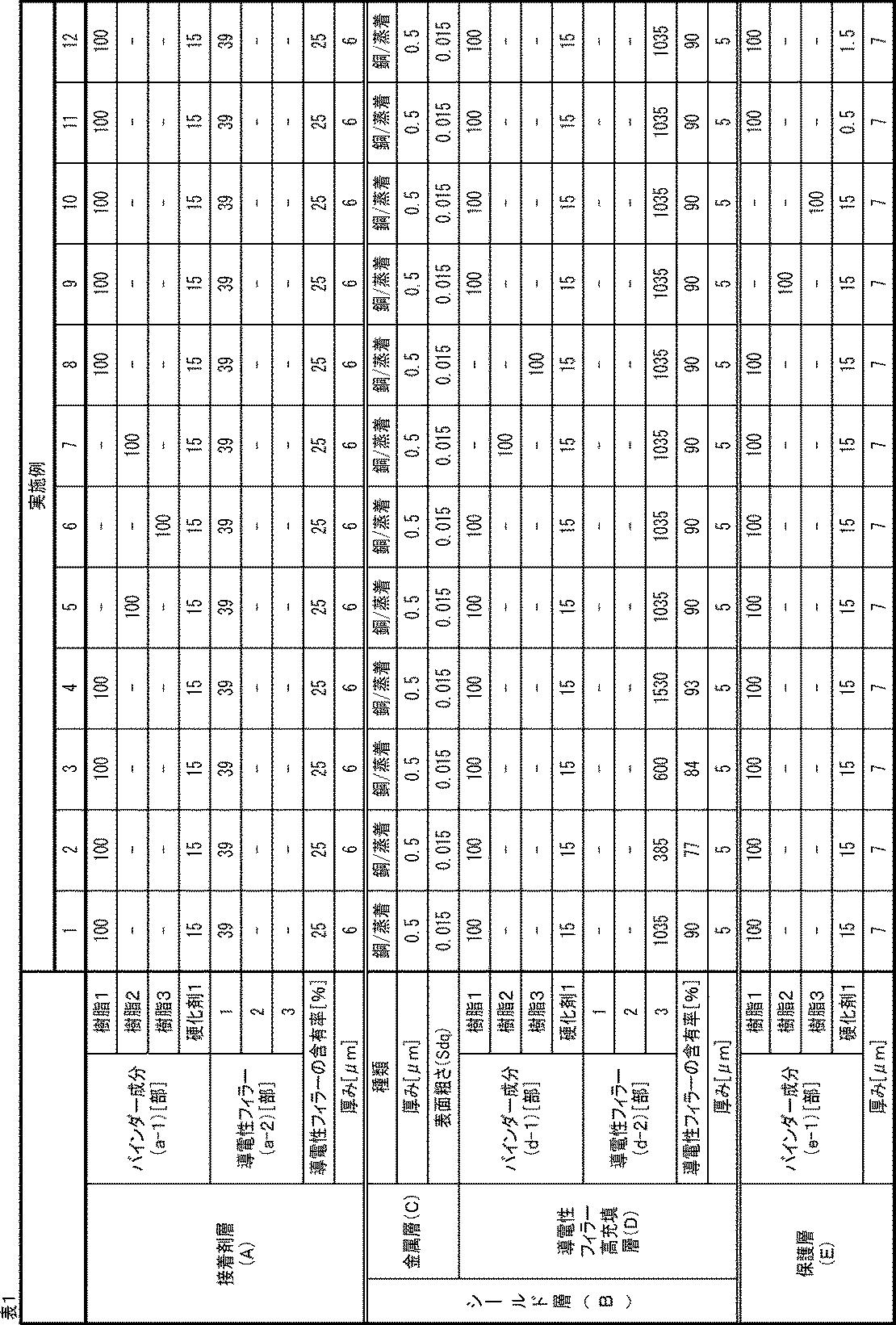

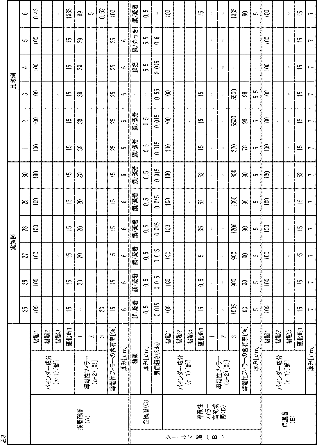
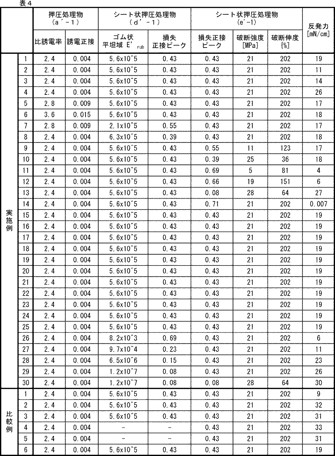
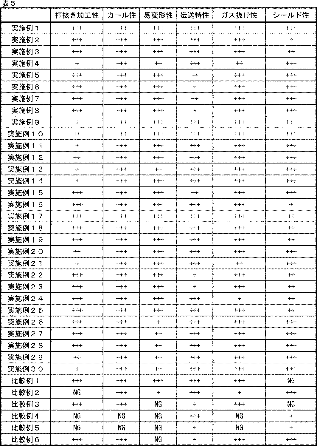
5:評価用試料、
8:カバーコート層、
10、15:配線回路基板、
11:絶縁性基材、
12:回路パターン、
12a:信号配線、
12b:グランド配線、
13:カバーコート層、
14:ビア、
20、21:シールド性配線基板、
41a:折曲部、
41b:左部、
41c:右部、
42:積層体、
44:基板、
45:シリコンゴム板、
50:ポリイミドフィルム、
51:銅メッキ膜、
52:スルーホール、
53:信号配線、
54:グランド配線、
55:グランドパターン、
56:裏面側グランドパターン、
60:台。
Claims (8)
- 接着剤層(A)と、当該接着剤層(A)の上に積層されたシールド層(B)とを備え、
シールド層(B)は、接着剤層(A)の上に積層された金属層(C)と、バインダー成分(d-1)と導電性フィラー(d-2)を含有し、金属層(C)の上に積層された導電性フィラー高充填層(D)とを有し、
当該導電性フィラー高充填層(D)の金属層(C)が形成されている側とは反対側の上には、金属層が形成されておらず、
導電性フィラー高充填層(D)100質量%に対し、導電性フィラー(d-2)の含有率が75~95質量%である電磁波シールドシート。 - 接着剤層(A)は、バインダー成分(a-1)を含み、
当該バインダー成分(a-1)を170℃30分の条件で押圧処理した押圧処理物(a’-1)の比誘電率が23℃、周波数28GHzにおいて1.0~3.5であり、押圧処理物(a’-1)の誘電正接が23℃、周波数28GHzにおいて0.0001~0.02であることを特徴とする請求項1記載の電磁波シールドシート。 - 接着剤層(A)は、導電性フィラー(a-2)を含有し、
導電性フィラー高充填層(D)100質量%に対し、導電性フィラー(d-2)の含有率が84~95質量%であり、
接着剤層(A)100質量%に対し、導電性フィラー(a-2)の含有率が15~45質量%であることを特徴とする請求項1または2記載の電磁波シールドシート。 - シールド層(B)の上に、更に、保護層(E)が積層されており、
保護層(E)は、バインダー成分(e-1)を含み、
当該バインダー成分(e-1)を170℃30分の条件で押圧処理したシート状押圧処理物(e’-1)の破断強度が15MPa以上であることを特徴とする請求項1~3のいずれか1項に記載の電磁波シールドシート。 - 170℃30分の条件で押圧処理した後の押圧処理物の反発力が0.01~30mN/cmであることを特徴とする請求項1~4のいずれか1項に記載の電磁波シールドシート。
- 絶縁性基材と、前記絶縁性基材上に形成された回路パターンと、前記絶縁性基材および前記回路パターン上に形成されたカバーコート層とを備える配線回路基板と、
電磁波シールドシートとを有し、
前記電磁波シールドシートは、前記カバーコート層上に請求項1~5のいずれか1項に記載の電磁波シールドシートの接着剤層(A)を用いて接合されたシールド性配線基板。 - 請求項6記載のシールド性配線基板を備える電子機器。
- 接着剤層(A)とシールド層(B)の積層構成を備える電磁波シールドシートの製造方法であって、
接着剤層(A)を形成する工程と、
シールド層(B)の一部として機能する金属層(C)を形成する工程と、
バインダー成分(d-1)と導電性フィラー(d-2)を含有する導電性フィラー含有組成物を塗工して、シールド層(B)の一部として機能する導電性フィラー高充填層(D)を形成する工程とを有し、
導電性フィラー高充填層(D)100質量%に対し、導電性フィラー(d-2)の含有率を75~95質量%とし、接着剤層(A)、金属層(C)、導電性フィラー高充填層(D)の順に積層し、前記導電性フィラー高充填層(D)の金属層(C)が形成されている側とは反対側の上には、金属層を形成しない、電磁波シールドシートの製造方法。
Priority Applications (2)
| Application Number | Priority Date | Filing Date | Title |
|---|---|---|---|
| CN202280005099.7A CN115702606B (zh) | 2021-03-19 | 2022-03-04 | 电磁波屏蔽片及其制造方法、屏蔽性配线基板、电子设备 |
| KR1020227038286A KR102683110B1 (ko) | 2021-03-19 | 2022-03-04 | 전자파 쉴드 시트 및 그 제조 방법, 쉴드성 배선 기판, 그리고 전자 기기 |
Applications Claiming Priority (2)
| Application Number | Priority Date | Filing Date | Title |
|---|---|---|---|
| JP2021-046610 | 2021-03-19 | ||
| JP2021046610A JP7001187B1 (ja) | 2021-03-19 | 2021-03-19 | 電磁波シールドシートおよびその製造方法、シールド性配線基板、並びに電子機器 |
Publications (1)
| Publication Number | Publication Date |
|---|---|
| WO2022196402A1 true WO2022196402A1 (ja) | 2022-09-22 |
Family
ID=80490543
Family Applications (1)
| Application Number | Title | Priority Date | Filing Date |
|---|---|---|---|
| PCT/JP2022/009527 Ceased WO2022196402A1 (ja) | 2021-03-19 | 2022-03-04 | 電磁波シールドシートおよびその製造方法、シールド性配線基板、並びに電子機器 |
Country Status (4)
| Country | Link |
|---|---|
| JP (1) | JP7001187B1 (ja) |
| KR (1) | KR102683110B1 (ja) |
| CN (1) | CN115702606B (ja) |
| WO (1) | WO2022196402A1 (ja) |
Cited By (1)
| Publication number | Priority date | Publication date | Assignee | Title |
|---|---|---|---|---|
| JP2024090181A (ja) * | 2022-12-22 | 2024-07-04 | Jx金属株式会社 | 銅箔、積層体、及びフレキシブルプリント配線板 |
Families Citing this family (3)
| Publication number | Priority date | Publication date | Assignee | Title |
|---|---|---|---|---|
| CN118633359A (zh) * | 2022-02-28 | 2024-09-10 | 拓自达电线株式会社 | 电磁波屏蔽薄膜 |
| KR102918756B1 (ko) * | 2023-09-05 | 2026-01-27 | 주식회사 휴나믹첨단소재 | 반도체 패키지 |
| KR102915490B1 (ko) * | 2023-12-01 | 2026-01-20 | 주식회사 휴나믹첨단소재 | Emi 차폐 필름이 적층된 반도체 패키지 |
Citations (4)
| Publication number | Priority date | Publication date | Assignee | Title |
|---|---|---|---|---|
| JP2012231021A (ja) * | 2011-04-26 | 2012-11-22 | Fujimori Kogyo Co Ltd | Fpc用電磁波シールド材 |
| WO2015151674A1 (ja) * | 2014-03-31 | 2015-10-08 | デクセリアルズ株式会社 | 導電性シールドテープ |
| WO2018147423A1 (ja) * | 2017-02-13 | 2018-08-16 | タツタ電線株式会社 | グランド部材、シールドプリント配線板及びシールドプリント配線板の製造方法 |
| JP2019021837A (ja) * | 2017-07-20 | 2019-02-07 | 信越ポリマー株式会社 | 電磁波シールドフィルム及びその製造方法、並びに電磁波シールドフィルム付きプリント配線板及びその製造方法 |
Family Cites Families (17)
| Publication number | Priority date | Publication date | Assignee | Title |
|---|---|---|---|---|
| JP4974803B2 (ja) | 2007-08-03 | 2012-07-11 | タツタ電線株式会社 | プリント配線板用シールドフィルム及びプリント配線板 |
| JP5139156B2 (ja) * | 2008-05-30 | 2013-02-06 | タツタ電線株式会社 | 電磁波シールド材及びプリント配線板 |
| JP5528857B2 (ja) * | 2010-03-11 | 2014-06-25 | タツタ電線株式会社 | 電磁波シールドフィルム、これを用いたフレキシブル基板及びその製造方法 |
| KR101361533B1 (ko) * | 2012-04-12 | 2014-02-13 | 한화엘앤씨 주식회사 | 전자기파 차폐 필름 제조방법 |
| JP6368711B2 (ja) * | 2013-05-28 | 2018-08-01 | タツタ電線株式会社 | 形状保持シールドフィルム、及びこの形状保持シールドフィルムを備えた形状保持型シールドフレキシブル配線板 |
| JP5975195B1 (ja) * | 2014-10-03 | 2016-08-23 | Dic株式会社 | シールドフィルム、シールドプリント配線板及びそれらの製造方法 |
| JP5854248B1 (ja) * | 2015-05-27 | 2016-02-09 | 東洋インキScホールディングス株式会社 | 導電性接着剤、ならびにそれを用いた導電性接着シートおよび電磁波シールドシート |
| KR102267570B1 (ko) | 2017-02-08 | 2021-06-18 | 타츠타 전선 주식회사 | 전자파 차폐 필름, 차폐 프린트 배선판 및 전자 기기 |
| KR102197471B1 (ko) * | 2017-12-18 | 2021-01-04 | 주식회사 잉크테크 | 전자파 차폐필름, 인쇄회로기판 제조방법 및 전자파 차폐필름 제조방법 |
| JP6970025B2 (ja) * | 2018-01-10 | 2021-11-24 | タツタ電線株式会社 | 電磁波シールドフィルム |
| JP6795732B2 (ja) * | 2018-04-26 | 2020-12-02 | 東洋インキScホールディングス株式会社 | フレキシブルプリント配線板、フレキシブルプリント配線板の製造方法及び電子部材 |
| JP7070061B2 (ja) * | 2018-05-11 | 2022-05-18 | Dic株式会社 | 導電性接着剤組成物 |
| JP7256618B2 (ja) * | 2018-08-29 | 2023-04-12 | タツタ電線株式会社 | 転写フィルム付電磁波シールドフィルム、転写フィルム付電磁波シールドフィルムの製造方法及びシールドプリント配線板の製造方法 |
| JP2021019012A (ja) * | 2019-07-17 | 2021-02-15 | 信越ポリマー株式会社 | 電磁波シールドフィルム、回路基板、及び回路基板の製造方法 |
| JP6645610B1 (ja) * | 2019-08-01 | 2020-02-14 | 東洋インキScホールディングス株式会社 | 電磁波シールドシート、および電磁波シールド性配線回路基板 |
| JP6624331B1 (ja) * | 2019-08-01 | 2019-12-25 | 東洋インキScホールディングス株式会社 | 電磁波シールドシート、および電磁波シールド性配線回路基板 |
| JP2020205399A (ja) * | 2019-09-12 | 2020-12-24 | 東洋インキScホールディングス株式会社 | 電磁波シールドシート、および電磁波シールド性配線回路基板 |
-
2021
- 2021-03-19 JP JP2021046610A patent/JP7001187B1/ja active Active
-
2022
- 2022-03-04 WO PCT/JP2022/009527 patent/WO2022196402A1/ja not_active Ceased
- 2022-03-04 CN CN202280005099.7A patent/CN115702606B/zh active Active
- 2022-03-04 KR KR1020227038286A patent/KR102683110B1/ko active Active
Patent Citations (4)
| Publication number | Priority date | Publication date | Assignee | Title |
|---|---|---|---|---|
| JP2012231021A (ja) * | 2011-04-26 | 2012-11-22 | Fujimori Kogyo Co Ltd | Fpc用電磁波シールド材 |
| WO2015151674A1 (ja) * | 2014-03-31 | 2015-10-08 | デクセリアルズ株式会社 | 導電性シールドテープ |
| WO2018147423A1 (ja) * | 2017-02-13 | 2018-08-16 | タツタ電線株式会社 | グランド部材、シールドプリント配線板及びシールドプリント配線板の製造方法 |
| JP2019021837A (ja) * | 2017-07-20 | 2019-02-07 | 信越ポリマー株式会社 | 電磁波シールドフィルム及びその製造方法、並びに電磁波シールドフィルム付きプリント配線板及びその製造方法 |
Cited By (1)
| Publication number | Priority date | Publication date | Assignee | Title |
|---|---|---|---|---|
| JP2024090181A (ja) * | 2022-12-22 | 2024-07-04 | Jx金属株式会社 | 銅箔、積層体、及びフレキシブルプリント配線板 |
Also Published As
| Publication number | Publication date |
|---|---|
| CN115702606A (zh) | 2023-02-14 |
| JP7001187B1 (ja) | 2022-01-19 |
| JP2022145270A (ja) | 2022-10-03 |
| KR20220161471A (ko) | 2022-12-06 |
| KR102683110B1 (ko) | 2024-07-10 |
| CN115702606B (zh) | 2025-08-08 |
Similar Documents
| Publication | Publication Date | Title |
|---|---|---|
| JP7363103B2 (ja) | 電磁波シールドシートおよびプリント配線板 | |
| WO2022196402A1 (ja) | 電磁波シールドシートおよびその製造方法、シールド性配線基板、並びに電子機器 | |
| KR102196833B1 (ko) | 전자파 차폐 시트, 및 전자파 차폐성 배선 회로 기판 | |
| JP6624331B1 (ja) | 電磁波シールドシート、および電磁波シールド性配線回路基板 | |
| CN111818723B (zh) | 电磁波屏蔽片及电磁波屏蔽性配线电路基板 | |
| TWI776347B (zh) | 電磁波屏蔽片及電磁波屏蔽性配線電路基板 | |
| JP2019220620A (ja) | 電磁波シールドシートおよびプリント配線板 | |
| JP2019220683A (ja) | 電磁波シールドシートおよびプリント配線板 | |
| JP7232995B2 (ja) | 電磁波シールドシートおよびその製造方法、シールド性配線基板、並びに電子機器 | |
| JP7452230B2 (ja) | 電磁波シールドシート、並びにプリント配線板およびその製造方法 | |
| JP2021027311A (ja) | 電磁波シールドシート、および電磁波シールド性配線回路基板 | |
| JP7559913B1 (ja) | 電磁波シールドシート、電磁波シールドシート付きプリント配線板、並びに電子機器 | |
| JP2020205399A (ja) | 電磁波シールドシート、および電磁波シールド性配線回路基板 | |
| JP7632575B2 (ja) | 電磁波シールドシート、および電磁波シールド性配線回路基板 | |
| JP2021027313A (ja) | 電磁波シールドシート、および電磁波シールド性配線回路基板 |
Legal Events
| Date | Code | Title | Description |
|---|---|---|---|
| ENP | Entry into the national phase |
Ref document number: 20227038286 Country of ref document: KR Kind code of ref document: A |
|
| 121 | Ep: the epo has been informed by wipo that ep was designated in this application |
Ref document number: 22771156 Country of ref document: EP Kind code of ref document: A1 |
|
| NENP | Non-entry into the national phase |
Ref country code: DE |
|
| 122 | Ep: pct application non-entry in european phase |
Ref document number: 22771156 Country of ref document: EP Kind code of ref document: A1 |
|
| WWG | Wipo information: grant in national office |
Ref document number: 202280005099.7 Country of ref document: CN |