WO2022196360A1 - 受光素子及び測定装置 - Google Patents
受光素子及び測定装置 Download PDFInfo
- Publication number
- WO2022196360A1 WO2022196360A1 PCT/JP2022/008858 JP2022008858W WO2022196360A1 WO 2022196360 A1 WO2022196360 A1 WO 2022196360A1 JP 2022008858 W JP2022008858 W JP 2022008858W WO 2022196360 A1 WO2022196360 A1 WO 2022196360A1
- Authority
- WO
- WIPO (PCT)
- Prior art keywords
- light
- light receiving
- optical system
- receiving element
- emitting element
- Prior art date
- Legal status (The legal status is an assumption and is not a legal conclusion. Google has not performed a legal analysis and makes no representation as to the accuracy of the status listed.)
- Ceased
Links
Images










Classifications
-
- G—PHYSICS
- G01—MEASURING; TESTING
- G01S—RADIO DIRECTION-FINDING; RADIO NAVIGATION; DETERMINING DISTANCE OR VELOCITY BY USE OF RADIO WAVES; LOCATING OR PRESENCE-DETECTING BY USE OF THE REFLECTION OR RERADIATION OF RADIO WAVES; ANALOGOUS ARRANGEMENTS USING OTHER WAVES
- G01S7/00—Details of systems according to groups G01S13/00, G01S15/00, G01S17/00
- G01S7/48—Details of systems according to groups G01S13/00, G01S15/00, G01S17/00 of systems according to group G01S17/00
- G01S7/481—Constructional features, e.g. arrangements of optical elements
-
- H—ELECTRICITY
- H10—SEMICONDUCTOR DEVICES; ELECTRIC SOLID-STATE DEVICES NOT OTHERWISE PROVIDED FOR
- H10F—INORGANIC SEMICONDUCTOR DEVICES SENSITIVE TO INFRARED RADIATION, LIGHT, ELECTROMAGNETIC RADIATION OF SHORTER WAVELENGTH OR CORPUSCULAR RADIATION
- H10F77/00—Constructional details of devices covered by this subclass
- H10F77/40—Optical elements or arrangements
Definitions
- the present invention relates to a light receiving element and a measuring device.
- Patent Literature 1 describes a distance measurement system that two-dimensionally scans a laser beam.
- An object of the present invention is to provide a high-quality light receiving device in view of the above points.
- the present invention provides, as one aspect, a changing section for changing the optical axis direction of light emitted from a light emitting element and reflected by an object to be emitted from an emission surface; and and a light receiving device having a detection surface for detecting light.
- a high quality light receiving device is provided.
- FIG. 1 is an explanatory diagram of an example of a measuring device.
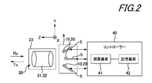
- FIG. 2 is an explanatory diagram of the mounting board 5 viewed from the X direction shown in FIG.
- FIG. 3A is an explanatory diagram of two-dimensional scanning by the measuring apparatus shown in FIG.
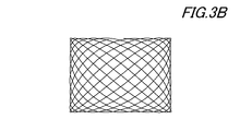
- FIG. 3B is an explanatory diagram of two-dimensional scanning in a certain frame by the measuring device shown in FIG.
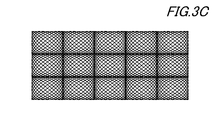
- FIG. 3C is an explanatory diagram of two-dimensional scanning in multiple channels by the measuring apparatus shown in FIG.
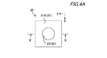
- FIG. 4A is a top view of the light receiver 20 according to the first embodiment.
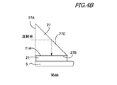
- FIG. 4B is a cross-sectional view of receiver 20 along line BB in FIG. 4A.
- FIG. 4C is an exploded perspective view of the receiver 20 shown in FIG. 4A.
- FIG. 4D is a cross-sectional view of the light receiving element 21 shown in FIG. 4A.
- FIG. 5A is a cross-sectional view of an example of the light receiver 20 according to the first embodiment.
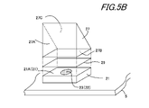
- FIG. 5B is an exploded perspective view of the receiver 20 shown in FIG. 5A.
- FIG. 6A is a horizontal cross-sectional view of an example of the light receiver 20 according to the first embodiment.
- FIG. 6B is an exploded perspective view of the receiver 20 shown in FIG. 6A.
- FIG. 7A is an explanatory diagram of how light is collected by the light-receiving optical system 32 according to the first embodiment.
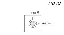
- FIG. 7B is an explanatory diagram of the light receiving window 23 and the focused spot in the light receiver 20 on the optical axis of the light receiving optical system 32 shown in FIG.
- FIG. 8 is an explanatory diagram of the output signal of the photodetector 20 according to the first embodiment.
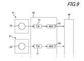
- FIG. 9 is an explanatory diagram of an example of a photodetector using the light receiving element of the first embodiment.
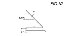
- FIG. 10 is a cross-sectional view of a light receiving device according to a modification of the first embodiment.
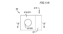
- FIG. 11A is a top view of the light receiver 20 according to the second embodiment.
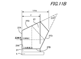
- FIG. 11B is a cross-sectional view of photodetector 20 along line BB in FIG. 11A.
- FIG. 11C is an exploded perspective view of the receiver 20 shown in FIG. 11A.
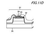
- FIG. 11D is a cross-sectional view of the light receiving element 21 shown in FIG. 11A.
- FIG. 11A is a top view of the light receiver 20 according to the second embodiment.
- FIG. 11B is a cross-sectional view of photodetector 20 along line BB in FIG. 11A.
- FIG. 11C is an exploded
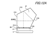
- FIG. 12A is a cross-sectional view of an example of the light receiver 20 according to the second embodiment.
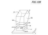
- FIG. 12B is an exploded perspective view of the receiver 20 shown in FIG. 12A.
- FIG. 13A is a horizontal cross-sectional view of an example of the photodetector 20 according to the second embodiment.
- FIG. 13B is an exploded perspective view of the receiver 20 shown in FIG. 13A.
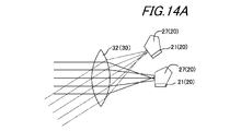
- FIG. 14A is an explanatory diagram of how light is collected by the light-receiving optical system 32 according to the second embodiment.
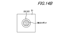
- FIG. 14B is an explanatory diagram of the light receiving window 23 and the focused spot in the light receiver 20 on the optical axis of the light receiving optical system 32 shown in FIG. 14A.
- FIG. 14A is an explanatory diagram of how light is collected by the light-receiving optical system 32 according to the second embodiment.
- FIG. 14B is an explanatory diagram of the light receiving window 23 and the focused spot in the light receiver 20 on the optical axis of the
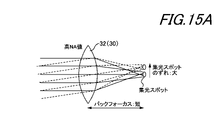
- FIG. 15A is a diagram for explaining condensed spot positions when the light receiving optical system 32 according to the second embodiment has a high NA value.
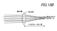
- FIG. 15B is a diagram for explaining the focused spot position when the light receiving optical system 32 shown in FIG. 15A has a low NA value.
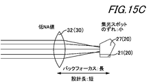
- FIG. 15C is a diagram for explaining the focused spot position when the prism 27 according to the present embodiment is used with the light receiving optical system 32 shown in FIG. 15A having a low NA value.
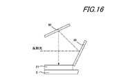
- FIG. 16 is a cross-sectional view of a light receiving device according to a modification of the second embodiment.
- FIG. 1 is an explanatory diagram of an example of a measuring device.
- each direction is defined as shown in FIG.
- the direction along the optical axis of the light receiving optical system 32 (or the light projecting optical system 31) (axis of rotational symmetry of the lens) is defined as the Z direction.
- An object 90 to be measured by the measuring device 1 is separated from the measuring device 1 in the Z direction.
- the direction perpendicular to the Z direction and in which the light projecting optical system 31 and the light receiving optical system 32 are arranged is defined as the X direction.
- a direction perpendicular to the Z direction and the X direction is defined as the Y direction.
- the measuring device 1 is a device for measuring the surface of the object 90. Specifically, the measuring device 1 emits a laser beam (Tx in FIG. 1) from the light emitting element 10, detects the reflected light (Rx in FIG. 1) reflected by the surface of the object 90 with the light receiver 20, This device calculates the distance to the object 90 based on the detection result.
- the measurement device 1 includes a light emitting element 10, a light receiver 20, an optical system 30, and a controller 40.
- the measuring device 1 also includes a mounting substrate 5 having a plurality of light emitting elements 10 and a plurality of light receivers 20 and a driving device 45 .
- the light emitting element 10 is an element that converts an electrical signal into an optical signal.
- the light emitting element 10 is an LD chip (LD: Laser Diode) and emits laser light.
- the light emitting element 10 emits pulsed light (Tx in FIG. 1) toward the surface of the object 90 .
- the light-emitting element 10 of this embodiment is composed of an edge-emitting semiconductor laser, is surface-mounted on the mounting substrate 5, and emits laser light parallel to the substrate surface.
- the light-emitting element 10 is not limited to an edge-emitting semiconductor laser, and the mounting method on the mounting board 5 is not limited to this.
- the light receiver 20 is a block that changes the direction of the optical signal from the light receiving optical system 32 and converts it into an electrical signal. Although details of the photodetector 20 will be described later, the photodetector 20 includes a PD chip (Photodiode). Light Receiver 20 The light receiver 20 is surface-mounted on the mounting board 5 . Note that the method of mounting the light receiver 20 is not limited to this. The mounting board 5 and the light receiver 20 are examples of the light receiving device in the present invention.
- the optical system 30 is an optical system for irradiating the object 90 with the light output from the light emitting element 10 and causing the light receiver 20 to receive the reflected light from the object 90 .
- the light emitting element 10 and the light receiver 20 are arranged at conjugate positions with respect to the optical system 30 .
- the optical system 30 of this embodiment has a light projecting optical system 31 and a light receiving optical system 32 .
- the light projecting optical system 31 is an optical system for irradiating the object 90 with the light output from the light emitting element 10 .
- a light-emitting element 10 is arranged in the focal plane of the light-projecting optical system 31 .
- the light projecting optical system 31 irradiates the object 90 with the laser light emitted from the light emitting element 10 as collimated light. Collimated light is emitted in a predetermined direction (predetermined angle) according to the positional relationship between the light emitting element 10 and the light projecting optical system 31 .
- the light emitting element 10 irradiates the object 90 with light through the light projecting optical system 31 .
- the light projecting optical system 31 is composed of a lens group composed of a plurality of (for example, 5 to 7) lenses (in FIG. 1, the lens group of the light projecting optical system 31 is simply shown). is being used).
- the light receiving optical system 32 is an optical system for causing the light receiver 20 to receive the reflected light from the object 90 .
- a light receiver 20 is arranged in the focal plane of the light receiving optical system 32 .
- the light-receiving optical system 32 collects the light reflected by the object 90 onto a predetermined light receiver 20 .
- the light receiver 20 receives reflected light from the object 90 via the light receiving optical system 32 .
- the light-receiving optical system 32 is also composed of a lens group composed of a plurality of (for example, 5 to 7) lenses.
- FIG. 1 simply shows the lens group of the light receiving optical system 32 .
- the light-projecting optical system 31 and the light-receiving optical system 32 are configured integrally, and their positional relationship is fixed. Specifically, a light projecting lens barrel that constitutes the light projecting optical system 31 and a light receiving lens barrel that constitutes the light receiving optical system 32 are fixed to a common optical frame 33 .
- the controller 40 is a control unit that controls the measuring device 1 .
- the controller 40 controls emission of laser light from the light emitting element 10 .
- the controller 40 calculates the distance to the object 90 based on the output signal of the light receiver 20 .
- the controller 40 determines the distance to the object 90 by measuring the time from when the light emitting element 10 projects a pulsed laser beam to when the light receiver 20 receives the reflected light. Measure. That is, the controller 40 measures the distance to the object 90, that is, the Z coordinate of the surface of the object 90 by the TOF method (time of flight) by controlling the light emitting element 10 and the light receiving device 20.
- the controller 40 measures the Z coordinate of the surface of the object 90 while scanning in the XY directions. , the X, Y, Z coordinates of the surface of the object 90 can be measured.
- the controller 40 has an arithmetic device 41 and a storage device 42 .
- the computing device 41 is, for example, a computing processing device such as a CPU or a GPU.
- the storage device 42 is configured by a main storage device and an auxiliary storage device, and stores programs and data. By executing the program stored in the storage device 42 by the arithmetic device 41, the arithmetic device 41 controls the emission of the laser light from the light emitting element 10, and based on the output signal of the light receiver 20, the target object. Calculate the distance to 90.
- the computing device 41 also calculates the X, Y, and Z coordinates of the surface of the object 90 based on the output signal of the light receiver 20 .
- the arithmetic device 41 may store the acquired coordinate data in the storage device 42 or in an external storage device.
- the data of the X, Y, and Z coordinates of many points on the surface of the object 90 become data representing a three-dimensional image (point group: point cloud) of the surface of the object 90 .
- the arithmetic device 41 may analyze the object 90 based on the three-dimensional image stored in the storage device 42 by executing the program stored in the storage device 42 .
- the mounting board 5 is a board on which a plurality of light emitting elements 10 and a plurality of light receivers 20 are mounted.
- a certain light receiver 20 is associated with a specific light emitting element 10 , and the detection position of the certain light receiver 20 is conjugate with the light emitting position of the specific light emitting element 10 .
- the light emitting element 10 emits laser light parallel to the surface of the mounting board 5, and the light receiver 20 receives light (reflected light) incident on the board surface of the mounting board 5 from a direction substantially parallel.
- the mounting substrate 5 has five light emitting elements 10 and five light receivers 20.
- the number of light emitting elements 10 and light receivers 20 is not limited to this.
- a plurality of light emitting elements 10 are arranged on the mounting substrate 5 at different positions in the X direction.
- a plurality of light receivers 20 are arranged on the mounting board 5 at different positions in the X direction.
- the mounting board 5 is provided with a light emitting side curved portion 6 and a light receiving side curved portion 7 .
- the light-emitting side curved portion 6 is a portion having an arcuate edge.
- the light-emitting side curved portion 6 is a portion for arranging a plurality of light-emitting elements 10 along the curvature of field of the light projecting optical system 31 .
- a plurality of light emitting elements 10 are arranged along the arcuate edge of the light emitting side curved portion 6 . Thereby, each light-emitting element 10 is arranged at an appropriate position and angle with respect to the light projecting optical system 31, and the influence of field curvature of the light projecting optical system 31 can be reduced.
- the light-receiving-side curved portion 7 is a portion having an arc-shaped edge, and is provided at a different position in the X direction from the light-emitting-side curved portion 6 .
- the light-receiving side curved portion 7 is a portion for arranging a plurality of light receivers 20 along the field curvature of the light-receiving optical system 32 .
- a plurality of light receivers 20 are arranged along the arcuate edge of the light receiving side curved portion 7 . Thereby, each light receiver 20 is arranged at an appropriate position and angle with respect to the light receiving optical system 32, and the influence of field curvature of the light receiving optical system 32 can be reduced.
- the mounting board 5 may not be provided with the light emitting side curved portion 6 or the light receiving side curved portion 7 .
- a plurality of light emitting elements 10 and a plurality of light receivers 20 are arranged along the edge of the mounting substrate 5 perpendicular to the Z direction.
- FIG. 2 is an explanatory diagram of the mounting substrate 5 viewed from the X direction shown in FIG.
- the light emitting side curved portion 6 and the light receiving side curved portion 7 of the mounting substrate 5 are omitted, and the light emitting element 10 and the light receiving device 20 are arranged along the edge of the mounting substrate 5 parallel to the X direction.
- the inclination of the mounting substrate 5 is emphasized here.
- the measuring device 1 has a plurality of mounting boards 5 (here, three mounting boards 5).
- the plurality of mounting boards 5 are arranged at different positions in the Y direction.
- a plurality of (here, five) light emitting elements 10 and a plurality of light receivers 20 are arranged on each mounting board 5 at different positions in the X direction. Therefore, a light-emitting element array is formed by arranging a plurality of (here, 15) light-emitting elements 10 in the X and Y directions, and a light-receiving element in which a plurality of light receivers 20 are arranged in the X and Y directions. An array is constructed.
- a plurality of mounting boards 5 are arranged at different angles with respect to the Z direction. Specifically, as shown in FIG. 2, the light emitting element 10 of each mounting board 5 faces the light projecting optical system 31, and the incident surface 27A (described later) of the light receiver 20 of each mounting board 5 is Each mounting substrate 5 is arranged at a different angle with respect to the Z direction so as to face the optical system 32 for light reception. As a result, the light-emitting element 10 and the light-receiving device 20 are arranged at appropriate positions and angles with respect to the optical system 30, so that the influence of field curvature of the optical system 30 can be reduced.
- the light emitting element 10 of each mounting board 5 is arranged so as to emit a laser beam parallel to the board surface of the mounting board 5 .
- each mounting board 5 is arranged so as to receive light (reflected light) incident from a direction substantially parallel to the board surface of the mounting board 5 . Since a plurality of (here, five) light-emitting elements 10 and a plurality (here, five) of light receivers 20 are mounted on the same substrate, the light-projecting optical system 31 and the light-receiving optical system 32 are separately installed. Therefore, even if the mounting substrate 5 is tilted with respect to the Z direction (the direction of the optical axis of the optical system 30), the respective light emitting elements 10 and the light receivers 20 are in a conjugate positional relationship with respect to the optical system 30. can be maintained.
- the mounting substrate 5 is provided with the light emitting side curved portion 6 and the light receiving side curved portion 7 as in the present embodiment, even if the mounting substrate 5 is tilted, the field curvature of the light projecting optical system 31 is followed. In addition, it is easy to arrange a plurality of light receivers 20 along the curvature of field of the light receiving optical system 32 .
- a plurality of mounting boards 5 may be arranged in parallel in the Z direction and arranged in parallel with each other. However, if the mounting boards 5 are arranged parallel to each other, each mounting board 5 should be arranged such that the light emitting element 10 and the light receiving device 20 are at appropriate positions and angles with respect to the optical system 30 . It is necessary to change the positions and angles of the light emitting element 10 and the light receiver 20 with respect to .
- the light emitting element 10 since the inclination of the mounting substrate 5 is made different, the light emitting element 10 emits a laser beam in parallel with the mounting substrate 5 and the can be configured to receive incident light (reflected light) from a direction substantially parallel to the . Therefore, in this embodiment, the plurality of light emitting elements 10 and the plurality of light receivers 20 can be arranged at different positions in the X direction and the Y direction at appropriate positions and angles with respect to the optical system 30 with a simple configuration. .
- a plurality of (here, three) mounting substrates 5 are integrally fixed, and the positional relationship between them is fixed. Specifically, the plurality of mounting boards 5 are fixed to a common board frame 8 . However, if the positional relationship between the plurality of light emitting elements 10 and the plurality of light receivers 20 can be fixed, the positional relationship between the plurality of light emitting elements 10 and the plurality of light receivers 20 may be fixed by other methods. Moreover, the measuring device 1 does not have to include a plurality of mounting substrates 5 .
- the drive device 45 (see FIG. 1) is a device that relatively moves the optical system 30 and the mounting substrate 5 (the light emitting element 10 and the light receiving device 20) in the XY directions.
- the driving device 45 relatively moves the optical system 30 and the mounting board 5 in the XY directions, thereby changing the positional relationship of the light emitting element 10 with respect to the optical system 30 and changing the irradiation angle of the laser light.
- a laser beam can be scanned.
- the driving device 45 moves at least one of the optical system 30 and the mounting board 5 , that is, one of the optical system 30 and the mounting board 5 , or both the optical system 30 and the mounting board 5 .
- the driving device 45 may move the optical system 30 in the XY directions with respect to the mounting board 5 , may move the optical system 30 in the XY directions with respect to the mounting board 5 , or may move the optical system 30 with respect to the mounting board 5 .
- at least one of the optical frame 33 and the substrate frame 8 is supported by the housing 3 in the X direction and the Y direction at predetermined resonance frequencies, respectively. 5 are vibrated in the X and Y directions at respective resonance frequencies.
- the driving device 45 is composed of, for example, a voice coil motor, but is not limited to this.
- the driving device 45 may be composed of a piezoelectric element.
- FIG. 3A is an explanatory diagram of two-dimensional scanning by the measuring device shown in FIG.
- the optical system 30 and the mounting substrate 5 by vibrating at least one of the optical system 30 and the mounting substrate 5 in the X direction and the Y direction at their respective resonance frequencies, the optical system 30 and the mounting substrate 5 (the light emitting element 10 or the light receiving device 20) are aligned in the figure.
- the controller 40 can calculate the position of the light emitting element 10 (or the light receiver 20) in the XY direction with respect to the optical system 30 based on the time t. That is, the controller 40 can calculate the direction in which the laser light is irradiated based on the time t.
- controller 40 uses a position detector (not shown) to detect the relative position in the XY direction between the optical frame 33 and the substrate frame 8 instead of calculating the direction in which the laser beam is irradiated based on the time t.
- the direction in which the laser beam is irradiated may be calculated based on this detection result.
- FIG. 3B is an explanatory diagram of two-dimensional scanning in a certain frame by the measuring device shown in FIG.
- the controller 40 acquires one frame (one three-dimensional image of the object 90) every predetermined time.
- the X, Y, Z coordinates of the surface of the object 90 are measured at a plurality of points on the Lissajous curve. This makes it possible to measure coordinates with increased resolution.
- the same Lissajous curve may be repeated for each frame. In this case, it is possible to measure the surface of the object 90 at the same position in each frame.
- the Lissajous curve may shift for each frame. In this case, in the next frame, measurements of the surface of the object 90 are possible so as to interpolate between the points measured in the previous frame.
- FIG. 3C is an explanatory diagram of two-dimensional scanning in multiple channels by the measuring device shown in FIG. As shown, in this embodiment, two-dimensional scanning is performed in different ranges for each channel. As a result, the surface of the object 90 can be measured over a wide range in the X and Y directions, and a wide FOV (field of view) can be realized.
- FOV field of view
- two-dimensional scanning does not have to be performed along the Lissajous curve.
- two-dimensional scanning may be performed by performing line scanning in the X direction (or Y direction) a plurality of times while shifting in the Y direction (or X direction).
- only one-dimensional scanning may be performed.
- scanning may not be performed.
- the measuring device 1 does not have to be equipped with the driving device 45 .
- the resolution of the point cloud is lowered compared to the present embodiment.
- FIG. 4A is a top view of the light receiver 20 according to the first embodiment.
- the light receiver 20 has a light receiving element 21 and a prism 27 .
- 4B is a cross-sectional view taken along line BB of FIG. 4A
- FIG. 4C is an exploded perspective view of photodetector 20 shown in FIG. 4A.
- 4D is a cross-sectional view of the light receiving element 21 shown in FIG. 4A.
- the light receiving element 21 is planarly mounted on the surface of the mounting substrate 5 . Specifically, the light-receiving element 21 is fixed on the surface of the mounting substrate 5 so that the surface of the mounting substrate 5 and the surface of the light-receiving element 21 that detects light (hereinafter referred to as a light-receiving surface 21A) are substantially parallel. be.
- the light receiving element 21 has a light receiving window 23 for receiving light on the light receiving surface 21A.
- the light receiving window 23 is a light receiving area provided on the light receiving surface 21A of the light receiving element 21 .
- the light receiving section 22 of the light receiving element 21 has a buffer layer, a light absorption layer, an intermediate layer, a doubling layer, and a window layer on the substrate, Further, it has a light receiving region and a guard ring around the periphery of the light receiving region, and has electrodes 24 and 25 on the front and back surfaces of the substrate, respectively.
- a protective layer is also formed on the light receiving surface 21A of the light receiving element 21 .
- the light receiving window 23 corresponds to a region inside the annular electrode 24 (electrode on the side of the light receiving surface 21A; electrode on the surface side of the substrate).
- the diameter of the light receiving window 23 is sometimes called the light receiving diameter. While the size of the light receiving element 21 is several millimeters square (for example, 5 mm square), the light receiving diameter is, for example, 500 ⁇ m. However, the light receiving element 21 and the size of the light receiving diameter are not limited to these.
- the height from the back surface of the light receiving element 21 to the surface of the light receiving window 23 provided in the center of the light receiving element 21 is drawn to be the highest.
- a flattening film, a protective film, and the like are formed on the surface 21A side. Therefore, the height from the rear surface of the light receiving element 21 to the light receiving surface 21A including the protective film and the like is substantially equal in the light receiving element 21.
- the prism 27 is a rectangular prism fixed to the light receiving element 21 and has the function of changing the optical axis direction of incident light by 90 degrees.
- Examples of the material of the prism 27 include optical glass, quartz, resin, and the like, and an appropriate material is adopted according to the required optical performance, usage conditions, design conditions, and the like.
- the prism 27 has an isosceles triangular cross-section as shown in FIGS. and a rectangular reflective surface 27C connected to the surface 27B.
- the incident surface 27A is a surface facing the light receiving optical system 32, and the reflected light condensed by the light receiving optical system 32 is incident thereon.
- the exit surface 27B is fixed to the light receiving element 21 and faces the light receiving section 22 .
- the area of the exit surface 27B is larger than that of the light receiving element 21 .
- the light incident on the incident surface 27A changes its optical axis direction by 90 degrees by the reflecting surface 27C, and is emitted from the emitting surface 27B so as to be perpendicular to the emitting surface 27B (Fig. 4B).
- An optical film can be attached or vapor-deposited to each of the entrance surface 27A, the exit surface 27B, and the reflection surface 27C.
- optical films include antireflection films, filters that absorb specific wavelengths, and reflective mirrors.
- the reflectance can be increased by depositing a reflective mirror on the reflective surface 27C.
- an antireflection film is formed on the emission surface 27B or the reflection surface 27C, the reflectance and transmittance of light on these surfaces can be adjusted.
- An appropriate method for fixing the output surface 27B to the light receiving element 21 is adopted according to the material of the prism 27, usage conditions, design conditions, and the like.
- Examples of bonding methods include a bonding method using low-melting glass, polymer, or film, anodic bonding, or direct bonding.
- the emission surface 27B may be fixed to the light receiving element 21 via a resin film.
- a resin film 29 is sandwiched between the emission surface 27B and the light receiving element 21, and the emission surface 27B and the light receiving element 21 are fixed with the resin film 29 interposed therebetween.
- the resin film 29 can be, for example, an optical film. In this case, by passing the light emitted from the emission surface 27B through the resin film 29, the refraction and reflection of unnecessary light are suppressed, or the absorption of a specific wavelength, the transmittance, etc. are adjusted, and the required optical performance is achieved. Obtainable.
- a gap may be provided between the exit surface 27B and the light receiving element 21 .
- the exit surface 27B is fixed to the light receiving element 21 via the mounting member 28.
- the mounting member 28 is provided along the peripheral edge of the light receiving element 21 , and a gap is formed by the thickness of the mounting member 28 between the light emitting surface 27B and the light receiving element 21 .
- the gap between the exit surface 27B and the light receiving element 21 is used to obtain required optical performance such as position adjustment between the focal point of the light condensed from the light receiving optical system 32 and the light receiving section 22. Further, by adjusting the thickness of the mounting member 28, it is also possible to adjust the mounting angle or mounting position of the prism 27 with respect to the light receiving element 21.
- FIG. 7A is an explanatory diagram of how light is collected by the light-receiving optical system 32 according to the first embodiment.
- FIG. 7B is an explanatory diagram of the light receiving window 23 and the focused spot in the light receiving element 21 on the optical axis of the light receiving optical system 32 shown in FIG. 7A.
- FIG. 8 is an explanatory diagram of the output signal of the photodetector 20 according to the first embodiment.
- the upper graph in each figure shows the current output from the light receiving section 22 .
- the light emitting element 10 emits pulsed light (Tx in FIG. 1), so that the light receiving element 21 is irradiated with a condensed light spot of the pulsed reflected light (Rx in FIG. 1). . Since the light-receiving window 23 is irradiated with the reflected light, the light-receiving section 22 outputs a pulsed current (output signal) as shown in the graph of FIG.
- the current output from the light receiving element 21 may be positive current or may be negative current.
- the light receiving section 22 outputs a current (output signal) corresponding to the light with which the light receiving window 23 is irradiated.
- the controller 40 can obtain the time t at which the pulsed reflected light is received based on the output signal. That is, the controller 40 can measure the time from when the light emitting element 10 projects the pulsed laser light until the light receiving element 21 receives the reflected light, and the distance to the object 90 can be measured. be able to.
- FIG. 9 is an explanatory diagram of an example of a photodetector using the photodetector of this embodiment.
- the mounting substrate 5 described above is provided with a circuit for configuring the photodetector 50 shown in FIG.
- the photodetector 50 has the photodetector 20 and the converter 51 described above.
- the converter 51 is a circuit that converts the signal output from the photodetector 20 from current to voltage.
- the photodetector 50 has a converter 51 for each light receiving element 21 .
- a conversion unit 51 shown in FIG. 9 is a circuit that converts the output signal output from the light receiving unit 22 from current to voltage.
- the conversion unit 51 is composed of a transimpedance amplifier (TIA).
- the photodetector 50 has an analog-digital conversion circuit 52 (ADC).
- An analog-digital conversion circuit 52 (ADC) is provided for each conversion section 51 .
- Each analog-digital conversion circuit 52 converts the voltage (analog signal) output from the conversion unit 51 into a digital signal, and outputs the signal to the controller 40 (arithmetic device 41).
- the controller 40 (arithmetic unit 41) compares the voltage value of the output signal with the threshold to obtain the time t during which the pulsed reflected light is received, and emits the pulsed laser light from the light emitting element 10. , the time until the light receiving element 21 receives the reflected light is calculated, and the distance to the object 90 is calculated.
- the prism 27 (corresponding to the changing portion in the present invention) that changes the optical axis direction of the light emitted from the light emitting element 10 and is reflected by the object and emits it from the emission surface 27B, and the prism 27 that emits the light and a light receiving element 21 having a light receiving surface 21A (corresponding to a detection surface) for detecting the light received.
- the light receiver 20 can be planarly mounted on the mounting board 5 . Therefore, there is no possibility that the fixation between the light receiving element 21 and the mounting substrate 5 is lost, and a high quality light receiving device can be obtained.
- the light receiving element 21 is attached to the surface of the mounting substrate 5 and electrically connected to the light receiving device 20 . Therefore, there is no possibility that the fixation between the light receiving element 21 and the mounting substrate 5 is lost, and a high quality light receiving device can be obtained.
- the prism 27 is a right angle prism.
- the light receiver 20 can change the direction of the optical axis of the reflected light with a simple configuration using a rectangular prism.
- the area of the output surface 27B is larger than the area of the light receiving surface 21A of the light receiving element 21.
- the prism 27 can be provided with at least one of an antireflection film and a deposited film mirror. Also, the prism 27 and the light receiving surface 21A of the light receiving element 21 may face each other with a resin film interposed therebetween. By including such an optical film in the light receiver 20, it is possible to obtain desired optical performance such as suppression of refraction or reflection of unnecessary light, absorption of specific wavelengths, adjustment of transmittance, and the like.
- the light receiver 20 may include a mounting member 28 that mounts the prism 27 to the light receiving element 21 while forming a gap between the light emitting surface 27B and the light receiving surface 21A. By forming the gap, it is possible to adjust the distance from the light receiving optical system 32 to the light receiving section 22 and obtain desired optical performance.
- the light-emitting element 10 and the light-receiving element 21 are both surface-mounted on the mounting substrate 5 and electrically connected. Therefore, there is no possibility that the light-receiving element 21 and the mounting board 5 are fixed together and the light-emitting element 10 and the mounting board 5 are fixed together, so that the photodetector 50 can be of high quality.
- the prism 27 is used as the changing portion.
- the invention is not limited to such configurations.
- a mirror 60 may be used instead of the prism 27 to change the optical axis direction of the reflected light.
- the conversion angle in the optical axis direction is not limited to 90 degrees.
- the prism 27 may be a different type of prism from the rectangular prism, or the mirror 60 may be used to set the change angle of the optical axis to an angle other than 90 degrees.
- FIG. 11A is a top view of the light receiver 20 according to the second embodiment.
- the light receiver 20 has a light receiving element 21 and a prism 27 .
- 11B is a cross-sectional view taken along line BB of FIG. 11A
- FIG. 11C is an exploded perspective view of photodetector 20 shown in FIG. 11A.
- 11D is a cross-sectional view of the light receiving element 21 shown in FIG. 11A.
- the prism 27 is a pentaprism fixed to the light receiving element 21, and has the function of reflecting the incident light twice and changing the optical axis direction by 90 degrees to emit the light.
- Examples of the material of the prism 27 include optical glass, quartz, resin, and the like, and an appropriate material is adopted according to the required optical performance, usage conditions, design conditions, and the like.
- the prism 27 has a pentagonal cross section as shown in FIGS. It has a rectangular reflective surface 27C and a reflective surface 27D respectively connected to the .
- the angle formed by the rectangular reflecting surfaces 27C and 27D is 22.5 degrees.
- the cross-sectional dimension of the prism 27 is as shown in FIG. 11B, and the ratio of the length d of the exit surface 27B in the normal direction of the entrance surface 27A to the total length of the prism 27 in the same direction is 1:1.41. .
- the incident surface 27A is a surface facing the light receiving optical system 32, and the reflected light condensed by the light receiving optical system 32 is incident thereon.
- the exit surface 27B is fixed to the light receiving element 21 and faces the light receiving section 22 .
- the area of the exit surface 27B is larger than that of the light receiving element 21 .
- the light incident on the incident surface 27A is reflected twice by the reflecting surfaces 27D and 27C, changes the direction of the optical axis by 90 degrees, and is emitted from the emitting surface 27B so as to be orthogonal to the emitting surface 27B (FIG. 11B). .
- An optical film can be attached or vapor-deposited to each of the entrance surface 27A, the exit surface 27B, and the reflection surfaces 27C and 27D.
- optical films include antireflection films, filters that absorb specific wavelengths, and reflective mirrors.
- the reflectance can be increased by depositing a reflective mirror on either of the reflective surfaces 27C and 27D.
- an anti-reflection film is formed on any one of the emission surface 27B and the reflection surfaces 27C and 27D, the reflectance and transmittance of light on these surfaces can be adjusted.
- the required optical performance can be obtained by forming an optical film on any one of the entrance surface 27A, the exit surface 27B, and the reflection surfaces 27C and 27D.
- the prism 27 (corresponding to the changing portion in the present invention) that reflects the light emitted from the light emitting element 10 and reflected by the object twice in the optical axis direction and emits it from the emission surface 27B, and the prism 27 A light receiving element 21 having a light receiving surface 21A (corresponding to a detection surface) for detecting emitted light is disclosed.
- the distance for the reflected light to reach the light receiving element 21 can be extended. That is, the back focal distance of the light receiving optical system 32 is extended, and the numerical aperture (NA value) of the light receiving optical system 32 can be reduced.
- FIG. 15A A specific example is shown in FIG.
- the light receiving optical system 32 has a short back focus and a large NA value (FIG. 15A)
- the deviation of the angle of the reflected light with respect to the optical axis of the light receiving optical system 32 greatly shifts the condensed spot position. Performance may be affected.
- an optical system with a long back focus and a small NA value FIG. 15B
- the influence of the deviation of the angle of the reflected light on the focused spot position can be reduced.
- the optical system can have a long back focus and allow a low NA value.
- the detection performance of the reflected light by the light receiving element 21 is maintained.
- the prism 27 is used to extend the optical path distance, the design length from the light receiving optical system 32 to the light receiving element 21 can be shortened (FIG. 15C). Therefore, the size reduction of the optical system 32 for light reception and the measuring apparatus 1 is attained.
- the prism 27 is a pentaprism.
- the light receiver 20 can change the direction of the optical axis of the reflected light with a simple structure using a pentaprism.
- the prism 27 is used as the changing portion.
- the invention is not limited to such configurations.
- two or more mirrors 60 may be used to change the optical axis direction of the reflected light, such as when a pentamirror is used instead of the prism 27 .
- the conversion angle in the optical axis direction between incident light and outgoing light is not limited to 90 degrees.
- the prism 27 may be a prism different from the pentaprism, or the mirror 60 may be used to set the angle of change of the optical axis to an angle other than 90 degrees.
Landscapes
- Engineering & Computer Science (AREA)
- Computer Networks & Wireless Communication (AREA)
- Physics & Mathematics (AREA)
- General Physics & Mathematics (AREA)
- Radar, Positioning & Navigation (AREA)
- Remote Sensing (AREA)
- Length Measuring Devices By Optical Means (AREA)
Abstract
受光装置は、発光素子(10)から照射され、対象物に反射された光の光軸方向を変更し、出射面(27B)から出射させる変更部(27)と、前記変更部(27)から出射された光を検出する検出面(21A)を有する受光素子(21)と、を備える。
Description
本発明は、受光素子及び測定装置に関する。
LiDAR(Light Detection and Ranging)などの距離測定システムでは、パルス状のレーザー光を投光してから反射光を受光するまでの時間を計測することによって、対象物までの距離を測定するTOF方式(Time of flight)が知られている。また、LiDARなどの距離測定システムでは、レーザー光を走査させて広い範囲で計測することも行われている。例えば特許文献1には、レーザー光を2次元走査させる距離測定システムが記載されている。
LiDARなどの距離測定システムを車両に搭載する場合には、距離測定システムを構成する発光素子、受光素子及び光学系などを狭い空間に配置する必要がある。また、1つの光学系に対して複数の受光素子を配置する場合には、光学系の光軸に対して受光素子をずらして配置する必要がある。この場合、受光チップの受光面を実装基板表面と直交するように立体実装を行う。立体実装では、実装基板の端面に受光チップの面を固定させるが、受光チップに対して基板の厚みは薄く、固着するための面積が非常に小さい。そのため、実装精度が悪くなったり、受光チップと基板との固着が失われたりするなど、実装後の品質低下を招く虞があった。
また、距離測定システムを構成する発光素子、受光素子及び光学系などを狭い空間に配置するためには、レンズを小口径にしたり、組レンズの全長を短くしたりと光学系を小型化する必要があるが、光学系を小型化すると光学性能を犠牲にしてしまう。そのため、物体の検出精度が悪くなるなど、装置の品質低下を招く虞があった。
本発明は、上記点に鑑み、品質の高い受光装置を提供することを目的とする。
上記目的を達成するため、本発明は一態様として、発光素子から照射され、対象物に反射された光の光軸方向を変更し、出射面から出射させる変更部と、前記変更部から出射された光を検出する検出面を有する受光素子と、を備える受光装置を提供する。
その他、本願が開示する課題、及びその解決方法は、発明を実施するための形態の欄、及び図面により明らかにされる。
本発明によれば、品質の高い受光装置が提供される。
以下、本発明を実施するための形態について図面を参照しつつ説明する。なお、以下の説明において、同一の又は類似する構成について共通の符号を付して重複した説明を省略することがある。
[第一実施形態]
<測定装置について>
図1は、測定装置の一例の説明図である。
<測定装置について>
図1は、測定装置の一例の説明図である。
以下の説明では、図1に示すように各方向を定めている。受光用光学系32(若しくは投光用光学系31)の光軸(レンズの回転対称軸)に沿った方向をZ方向とする。なお、測定装置1の測定対象となる対象物90は、測定装置1に対してZ方向に離れている。また、Z方向に垂直な方向であって、投光用光学系31と受光用光学系32の並ぶ方向をX方向とする。また、Z方向及びX方向に垂直な方向をY方向とする。
測定装置1は、対象物90の表面を測定するための装置である。具体的には、測定装置1は、発光素子10からレーザー光(図1のTx)を射出し、対象物90の表面で反射した反射光(図1のRx)を受光器20によって検出し、検出結果に基づいて、対象物90までの距離を算出する装置である。測定装置1は、発光素子10と、受光器20と、光学系30と、コントローラー40とを備える。また、測定装置1は、複数の発光素子10と複数の受光器20を有する実装基板5と、駆動装置45を備えている。
発光素子10は、電気信号を光信号に変換する素子である。例えば、発光素子10は、LDチップ(LD:Laser Diode)であり、レーザー光を射出する。本実施形態では、発光素子10は、対象物90の表面に向かってパルス光(図1のTx)を射出する。本実施形態の発光素子10は、端面発光半導体レーザーで構成されており、実装基板5に表面実装されており、基板面に平行にレーザー光を射出する。なお、発光素子10は、端面発光半導体レーザーに限られるものではなく、実装基板5への実装方法もこれに限られるものではない。
受光器20は、受光用光学系32からの光信号の方向を変更しつつ、電気信号に変換するブロックである。受光器20の詳細は後述するが、PDチップ(Photodiode)を含んで構成される。受光器20受光器20は、実装基板5に対して表面実装されている。なお、受光器20の実装方法はこれに限られるものではない。なお、実装基板5及び受光器20は、本発明における受光装置の一例である。
光学系30は、発光素子10から出力される光を対象物90に向かって照射するとともに、対象物90からの反射光を受光器20に受光させるための光学系である。発光素子10と受光器20は、光学系30に対して共役の位置に配置されている。本実施形態の光学系30は、投光用光学系31と、受光用光学系32とを有する。
投光用光学系31は、発光素子10から出力される光を対象物90に向かって照射するための光学系である。投光用光学系31の焦点面内に発光素子10が配置されている。投光用光学系31は、発光素子10から射出されたレーザー光をコリメート光として対象物90に照射する。発光素子10と投光用光学系31との位置関係に応じた所定の方向(所定の角度)にコリメート光が照射される。発光素子10は投光用光学系31を介して対象物90に光を照射する。投光用光学系31は、複数枚(例えば5~7枚)のレンズで構成されたレンズ群によってそれぞれ構成されている(図1では、投光用光学系31のレンズ群が簡易的に示されている)。
受光用光学系32は、対象物90からの反射光を受光器20に受光させるための光学系である。受光用光学系32の焦点面内に受光器20が配置されている。受光用光学系32は、対象物90の反射光を所定の受光器20に集光する。受光器20は受光用光学系32を介して対象物90からの反射光を受光する。受光用光学系32も、投光用光学系31と同様に、複数枚(例えば5~7枚)のレンズで構成されたレンズ群によってそれぞれ構成されている。図1では、受光用光学系32のレンズ群が簡易的に示されている。
投光用光学系31と受光用光学系32は、一体的に構成されており、互いの位置関係が固定されている。具体的には、投光用光学系31を構成する投光用鏡筒と、受光用光学系32を構成する受光用鏡筒とが共通の光学用フレーム33に固定されている。
コントローラー40は、測定装置1の制御を司る制御部である。コントローラー40は、発光素子10からのレーザー光の射出を制御する。また、コントローラー40は、受光器20の出力信号に基づいて、対象物90までの距離を算出する。具体的には、コントローラー40は、発光素子10からパルス状のレーザー光を投光してから、受光器20が反射光を受光するまでの時間を計測することによって、対象物90までの距離を測定する。すなわち、コントローラー40は、発光素子10及び受光器20を制御することによって、TOF方式(Time of flight)により対象物90までの距離、すなわち対象物90の表面のZ座標を測定する。また、所定の方向にレーザー光が照射され、所定の方向の反射光を受光することを利用して、コントローラー40は、XY方向に走査しながら対象物90の表面のZ座標を測定することによって、対象物90の表面のX,Y,Z座標を測定可能である。
コントローラー40は、演算装置41と、記憶装置42とを有する。演算装置41は、例えばCPU、GPUなどの演算処理装置である。記憶装置42は、主記憶装置と補助記憶装置とにより構成され、プログラムやデータを記憶する装置である。記憶装置42に記憶されているプログラムを演算装置41が実行することにより、演算装置41は、発光素子10からのレーザー光の射出を制御するとともに、受光器20の出力信号に基づいて、対象物90までの距離を算出する。また、演算装置41は、受光器20の出力信号に基づいて、対象物90の表面のX,Y,Z座標を算出する。演算装置41は、取得した座標データを記憶装置42に記憶しても良いし、外部の記憶装置に記憶しても良い。対象物90の表面上の多数の点のX,Y,Z座標のデータは、対象物90の表面の3次元画像(点群:点クラウド)を示すデータとなる。演算装置41は、記憶装置42に記憶されているプログラムを演算装置41が実行することにより、記憶装置42に記憶された3次元画像に基づいて、対象物90の解析を行っても良い。
実装基板5は、複数の発光素子10と、複数の受光器20とを実装した基板である。或る受光器20は特定の発光素子10に対応付けられており、或る受光器20の検出位置は、特定の発光素子10の発光位置と共役である。本実施形態では、発光素子10と受光器20との対が複数あり、複数のチャンネルで対象物90の表面を測定可能である。なお、発光素子10は、実装基板5の基板面に平行にレーザー光を射出し、受光器20は、実装基板5の基板面にほぼ平行な方向から入射する光(反射光)を受光する。
図1に示すように、実装基板5は、5個の発光素子10と、5個の受光器20とを有する。但し、発光素子10や受光器20の数は、これに限られるものではない。実装基板5には、複数の発光素子10がX方向の異なる位置に配置されている。また、実装基板5には、複数の受光器20がX方向の異なる位置に配置されている。
図1に示すように、実装基板5には、発光側湾曲部6と、受光側湾曲部7とが設けられている。
発光側湾曲部6は、円弧状の縁を有する部位である。発光側湾曲部6は、投光用光学系31の像面湾曲に沿うように複数の発光素子10を配置するための部位である。発光側湾曲部6の円弧状の縁に沿って複数の発光素子10が配置されている。これにより、それぞれの発光素子10は、投光用光学系31に対して、適切な位置及び角度に配置され、投光用光学系31の像面湾曲の影響を軽減できる。
受光側湾曲部7は、円弧状の縁を有する部位であり、発光側湾曲部6とはX方向の異なる位置に設けられている。受光側湾曲部7は、受光用光学系32の像面湾曲に沿うように複数の受光器20を配置するための部位である。受光側湾曲部7の円弧状の縁に沿って、複数の受光器20が配置されている。これにより、それぞれの受光器20は、受光用光学系32に対して、適切な位置及び角度に配置され、受光用光学系32の像面湾曲の影響を軽減できる。
但し、実装基板5に発光側湾曲部6や受光側湾曲部7が設けられていなくても良い。この場合、実装基板5のZ方向に垂直な縁に沿って、複数の発光素子10や複数の受光器20が配列される。
図2は、図1に示すX方向から見た実装基板5の説明図である。ここでは説明のため、実装基板5の発光側湾曲部6や受光側湾曲部7を省略し、実装基板5のX方向に平行な縁に沿って発光素子10及び受光器20が配置されているものとする。なお、ここでは説明のため、実装基板5の傾きが強調されて図示されている。
図2に示すように、測定装置1は、複数枚の実装基板5(ここでは3枚の実装基板5)を有している。複数枚の実装基板5は、Y方向の異なる位置に配置されている。各実装基板5には、図1に示すように、X方向の異なる位置に複数(ここでは5個)の発光素子10及び複数の受光器20が配置されている。このため、X方向及びY方向に複数(ここでは15個)の発光素子10を配列させた発光素子アレイが構成されるとともに、X方向及びY方向に複数の受光器20を配列させた受光素子アレイが構成される。ここでは、5×3の15チャンネル(X方向に5チャンネル、Y方向に3チャンネル)で対象物90の表面を測定する。
複数枚の実装基板5は、Z方向に対して異なる角度で配置されている。具体的には、図2に示すように、各実装基板5の発光素子10が投光用光学系31を向くように、また、各実装基板5の受光器20の入射面27A(後述)が受光用光学系32を向くように、それぞれの実装基板5が、Z方向に対して異なる角度で配置されている。これにより、発光素子10及び受光器20が光学系30に対してそれぞれ適切な位置及び角度に配置されるため、光学系30の像面湾曲の影響を軽減できる。各実装基板5の発光素子10は、その実装基板5の基板面に平行にレーザー光を射出するように配置されている。また、各実装基板5の受光器20は、その実装基板5の基板面にほぼ平行な方向から入射する光(反射光)を受光するように配置されている。複数(ここでは5個)の発光素子10及び複数(ここでは5個)の受光器20が同じ基板に実装されているため、また、投光用光学系31と受光用光学系32がそれぞれ別に設けられているため、実装基板5をZ方向(光学系30の光軸の方向)に対して傾けても、それぞれの発光素子10と受光器20とを光学系30に対して共役の位置関係に維持することができる。なお、本実施形態のように実装基板5に発光側湾曲部6及び受光側湾曲部7が設けられていれば、実装基板5を傾けても、投光用光学系31の像面湾曲に沿うように複数の発光素子を配置させ易く、また、受光用光学系32の像面湾曲に沿うように複数の受光器20を配置させ易い。
なお、複数の実装基板5をZ方向に平行に配置し、互いに平行に配置しても良い。但し、仮に各実装基板5を互いに平行に配置した場合には、実装基板5ごとに、発光素子10及び受光器20が光学系30に対して適切な位置及び角度になるように、実装基板5に対する発光素子10及び受光器20の位置及び角度を異ならせる必要がある。これに対し、本実施形態では、実装基板5の傾きを異ならせるため、いずれの実装基板5においても、発光素子10が実装基板5に平行にレーザー光を射出し、受光器20が実装基板5にほぼ平行な方向から入射する光(反射光)を受光するように構成することができる。このため、本実施形態では、複数の発光素子10及び複数の受光器20を、X方向及びY方向の異なる位置に、簡易な構成で、光学系30に対して適切な位置及び角度に配置できる。
複数(ここでは3枚)の実装基板5は、一体的に固定されており、互いの位置関係が固定されている。具体的には、複数の実装基板5は、共通の基板用フレーム8に固定されている。但し、複数の発光素子10及び複数の受光器20の位置関係を固定できれば、他の方法で複数の発光素子10及び複数の受光器20の位置関係を固定しても良い。また、測定装置1が複数の実装基板5を備えていなくても良い。
駆動装置45(図1参照)は、光学系30と実装基板5(発光素子10及び受光器20)とをXY方向に相対移動させる装置である。駆動装置45が光学系30と実装基板5とをXY方向に相対移動させることによって、光学系30に対する発光素子10の位置関係を変化させ、レーザー光の照射される角度を変化させ、これにより、レーザー光を走査させることができる。
駆動装置45は、光学系30と実装基板5の少なくとも一方、すなわち光学系30と実装基板5の一方、又は光学系30と実装基板5の両方を移動させる。なお、駆動装置45は、光学系30を実装基板5に対してXY方向に移動させても良いし、実装基板5に対して光学系30をXY方向に移動させても良いし、光学系30をX方向(又はY方向)に移動させつつ実装基板5をY方向(又はX方向)に移動させても良い。本実施形態では、光学用フレーム33と基板用フレーム8の少なくとも一方がX方向及びY方向にそれぞれ所定の共振周波数で筐体3に支持されており、駆動装置45は、光学系30と実装基板5の少なくとも一方をX方向及びY方向にそれぞれの共振周波数で振動させている。駆動装置45は、例えばボイスコイルモータで構成されるが、これに限られるものではない。例えば、駆動装置45は、圧電素子によって構成されても良い。
図3Aは、図1に示す測定装置による2次元走査の説明図である。本実施形態では、光学系30と実装基板5の少なくとも一方をX方向及びY方向にそれぞれの共振周波数で振動させることによって、光学系30と実装基板5(発光素子10又は受光器20)が図3Aに示すようにリサージュ曲線に沿ってXY方向に相対的に変位する。リサージュ曲線は、X=Asin(at+δ),Y=Bsin(bt)のグラフとなる。ここで、a及びbは、それぞれX方向及びY方向の周波数であり、tは時間であり、δは位相差である。既に説明した通り、光学用フレーム33と基板用フレーム8の少なくとも一方がX方向及びY方向にそれぞれ所定の共振周波数で支持されているため、a及びbは既知の値となる。また、駆動装置45が所定の振幅で光学用フレーム33又は基板用フレーム8を共振させることによってA,Bは既知の値となり、駆動装置45によるX方向及びY方向の駆動タイミングに基づいてδは既知の値となる。このため、コントローラー40は、時間tに基づいて、光学系30に対する発光素子10(若しくは受光器20)のXY方向の位置を算出可能である。つまり、コントローラー40は、時間tに基づいて、レーザー光が照射される方向を算出可能である。なお、コントローラー40は、時間tに基づいて、レーザー光が照射される方向を算出する代わりに、不図示の位置検出器によって光学用フレーム33と基板用フレーム8とのXY方向の相対位置を検出し、この検出結果に基づいてレーザー光が照射される方向を算出しても良い。
図3Bは、図1に示す測定装置による或るフレームにおける2次元走査の説明図である。コントローラー40は、所定時間毎に、1枚のフレーム(対象物90の1枚の3次元画像)を取得する。1枚のフレーム(1枚の3次元画像)の測定ごとに、リサージュ曲線上の複数の点において対象物90の表面のX,Y,Z座標を測定する。これにより、解像度を高めて座標を測定可能である。なお、フレーム毎に同じリサージュ曲線が反復されても良い。この場合、各フレームにおいて、同じ位置で対象物90の表面の測定が可能になる。一方、フレーム毎にリサージュ曲線がシフトしても良い。この場合、次のフレームにおいて、前のフレームで測定した点群の間を補間するように、対象物90の表面の測定が可能になる。
図3Cは、図1に示す測定装置による複数チャンネルにおける2次元走査の説明図である。図示するように、本実施形態では、チャンネル毎に異なる範囲で2次元走査が行われる。これにより、X方向及びY方向の広い範囲において、対象物90の表面の測定が可能になり、広いFOV(field of view)を実現できる。
なお、2次元走査がリサージュ曲線に沿って行われなくても良い。例えば、X方向(又はY方向)のライン走査をY方向(又はX方向)にずらして複数回行うことによって、2次元走査が行われても良い。また、2次元走査ではなく、1次元走査が行われるだけでも良い。また、走査が行われなくても良い。走査を行わない場合には、測定装置1は駆動装置45を備えていなくても良い。但し、走査を行わない場合には、本実施形態と比べて、点群の解像度が低下する。
<受光器について>
本実施形態による受光器20について説明する。
本実施形態による受光器20について説明する。
図4Aは、第一実施形態に係る受光器20を上から見た図である。受光器20は、受光素子21及びプリズム27を有する。図4Bは、図4AのB-B線による断面図であり、図4Cは図4Aに示す受光器20の分解斜視図である。また、図4Dは、図4Aに示す受光素子21の断面図である。
受光素子21は、実装基板5の表面に平面実装される。詳細には、受光素子21は、実装基板5の表面と受光素子21における光を検知する面(以下、受光面21Aと称する)とが略平行となるように、実装基板5表面上に固定される。受光素子21は、受光面21Aにおいて、光を受光する受光窓23を有する。受光窓23は、受光素子21の受光面21Aに設けられた受光領域である。例えば受光素子21がアバランシェフォトダイオード(APD:Avalanche Photodiode)の場合、受光素子21の受光部22は、基板上にバッファ層、光吸収層、中間層、倍増層、窓層を有しており、更に受光領域と受光領域の外周部のガードリングとを有しており、基板表面及び裏面にそれぞれ電極24及び電極25を有している。また、受光素子21の受光面21Aには保護層も形成される。ここでは、受光窓23は、環状の電極24(受光面21A側の電極;基板表面側の電極)の内側の領域に相当する。受光窓23の直径のことを受光径と呼ぶことがある。受光素子21の大きさが数ミリ角(例えば5mm角)であるのに対し、受光径は例えば500μmである。但し、受光素子21や受光径の大きさは、これに限られるものではない。
なお、図4Dにおいては、便宜上、受光素子21の裏面から、受光素子21の中央に設けられた受光窓23の表面までの高さが、最も高くなるよう描いているが、実際には、受光面21A側には、平坦化膜や保護膜等(不図示)が形成されている。このため、受光素子21の裏面から、保護膜等を含む受光面21Aまでの高さは受光素子21において略等しい。
プリズム27は、受光素子21に固定された直角プリズムであり、入射した光の光軸方向を90度変える機能を有する。プリズム27の材質として、光学ガラスや石英、樹脂などが挙げられるが、要求される光学性能、使用条件及び設計条件等に応じて適切なものが採用される。
プリズム27は、図4~図6に示すように二等辺三角形状の断面を有しており、互いに直交する2つの矩形面(入射面27A及び出射面27Bとする)と、入射面27A及び出射面27Bに接続する矩形の反射面27Cとを有する。
入射面27Aは、受光用光学系32に対向する面であり、受光用光学系32によって集光された反射光が入射する。出射面27Bは、受光素子21に固定され、受光部22と対向する。出射面27Bの面積は、受光素子21よりも大きい。
入射面27Aに入射した光は、反射面27Cによって光軸の方向を90度変え、出射面27Bから、出射面27Bと直交するように出射する(図4B)。
入射面27A、出射面27B及び反射面27Cには、いずれにも光学膜を貼付または蒸着させることが可能である。光学膜の例としては、反射防止膜、特定の波長を吸収するフィルタ、反射ミラーなどがある。例えば、反射面27Cに反射ミラーを成膜することにより、反射率を増加させることができる。また、出射面27Bまたは反射面27Cに反射防止膜を成膜した場合には、これらの面における光の反射率、透過率を調整することができる。このように、入射面27A、出射面27Bまたは反射面27Cに光学膜を成膜することにより、要求される光学性能を得ることができる。
出射面27Bの受光素子21に対する固定方法は、プリズム27の材質、使用条件及び設計条件等に応じて適切なものが採用される。例えば、低融点ガラスや、ポリマ、フィルムを用いて接着する方法や、陽極接合または直接接合などが、接合方法の例として挙げられる。
出射面27Bが樹脂膜を介して受光素子21に固定されてもよい。図5A、図5Bに示す例では、出射面27Bと受光素子21との間に樹脂膜29が挟まれ、樹脂膜29を介して出射面27Bと受光素子21とが固定される。樹脂膜29は、例えば光学膜とすることができる。この場合、出射面27Bから出射した光を樹脂膜29に通すことにより、不要な光の屈折、反射の抑制、または特定の波長の吸収、透過率の調整などを行い、要求される光学性能を得ることができる。
出射面27Bと受光素子21との間には、空隙が設けられてもよい。図6A、図6Bに示す例では、出射面27Bは、受光素子21に対して取付部材28を介して固定される。取付部材28は受光素子21の周縁部に沿って設けられており、出射面27Bと受光素子21との間には、取付部材28の厚みによって空隙が形成される。出射面27Bと受光素子21との間の空隙は、受光用光学系32から集光された光の焦点と受光部22との位置調整など、要求される光学性能を得るために利用される。また、取付部材28の厚みを調整することにより、プリズム27の受光素子21に対する取付角度または取付位置を調整することも可能である。
図7Aは、第一実施形態に係る受光用光学系32による集光の様子の説明図である。図7Bは、図7Aに示す受光用光学系32の光軸上の受光素子21における受光窓23と集光スポットの説明図である。
1つの受光用光学系32に対して複数の受光器20が配置されるため、図7Aに示すように、受光用光学系32に対して、光軸上に配置される受光器20とは別に、光軸から外れた位置に配置される受光器20が存在する。図7Aでは、受光用光学系32の光軸から外れた受光器20が1つだけ描かれているが、受光用光学系32の光軸から外れた受光器20は複数存在しており、更に、受光用光学系32の光軸に対する外れ方も互いに異なっている。受光用光学系32から出射した反射光は、プリズム27を介して受光素子21の受光面21Aに集光され、集光スポットを形成する(図7B)。
図8は、第一実施形態に係る受光器20の出力信号の説明図である。それぞれの図の上側のグラフは、受光部22から出力される電流を示している。既に説明した通り、本実施形態では、発光素子10はパルス光(図1のTx)を射出するため、パルス状の反射光(図1のRx)の集光スポットが受光素子21に照射される。受光窓23に反射光が照射されるため、受光部22は、図8のグラフに示すように、パルス状の電流(出力信号)を出力する。
なお、受光素子21から出力される電流は、プラス側の電流になる場合もあるし、マイナス側の電流になる場合もある。受光部22は、受光窓23に照射された光に応じた電流(出力信号)を出力する。
コントローラー40は、出力信号に基づいて、パルス状の反射光を受光した時間tを求めることができる。つまり、コントローラー40は、発光素子10からパルス状のレーザー光を投光してから、受光素子21が反射光を受光するまでの時間を計測することができ、対象物90までの距離を測定することができる。
図9は、本実施形態の受光装置を用いた光検出装置の一例の説明図である。例えば、前述の実装基板5には、図9に示す光検出装置50を構成するための回路が設けられている。
光検出装置50は、上記の受光器20と、変換部51とを有する。変換部51は、受光器20から出力される信号を電流から電圧に変換する回路である。光検出装置50は、すなわち受光素子21毎に変換部51を有している。図9に示す変換部51は、受光部22から出力される出力信号を電流から電圧に変換する回路である。変換部51は、トランスインピーダンス・アンプ(TIA)で構成される。
光検出装置50は、アナログ-デジタル変換回路52(ADC)を有している。アナログ-デジタル変換回路52(ADC)は、変換部51毎に設けられている。それぞれのアナログ-デジタル変換回路52は、変換部51から出力される電圧(アナログ信号)をデジタル信号に変換し、コントローラー40(演算装置41)に信号を出力する。コントローラー40(演算装置41)は、出力信号の電圧値と閾値とを比較することによって、パルス状の反射光を受光した時間tを求め、発光素子10からパルス状のレーザー光を投光してから、受光素子21が反射光を受光するまでの時間を算出し、対象物90までの距離を算出する。
<効果>
上記実施形態では、発光素子10から照射され対象物に反射された光の光軸方向を変更し、出射面27Bから出射させるプリズム27(本発明における変更部に相当)と、プリズム27から出射された光を検出する受光面21A(検出面に相当)を有する受光素子21と、を備える。
上記実施形態では、発光素子10から照射され対象物に反射された光の光軸方向を変更し、出射面27Bから出射させるプリズム27(本発明における変更部に相当)と、プリズム27から出射された光を検出する受光面21A(検出面に相当)を有する受光素子21と、を備える。
上記構成とすることによって、受光器20を実装基板5に対して平面実装することが可能となる。そのため、受光素子21と実装基板5との固着が失われたりする虞が無く、品質の高い受光装置とすることができる。
受光器20は、受光素子21が実装基板5の表面に取り付けられ、電気的に接続される。そのため、受光素子21と実装基板5との固着が失われたりする虞が無く、品質の高い受光装置とすることができる。
プリズム27は直角プリズムである。受光器20は、直角プリズムを用いた簡易な構成により、反射光の光軸方向の変更を可能としている。
出射面27Bの面積は、受光素子21の受光面21Aの面積よりも大きい。プリズム27を大型にすることで、反射光の受光束または受光量を増加させることができる。受光部22に入射する光量が増し、受光素子21の検出精度が向上する。
プリズム27は、反射防止膜及び蒸着膜ミラーの少なくとも1つを備えることができる。また、プリズム27と受光素子21の受光面21Aとが樹脂膜を介して対向してもよい。受光器20がこのような光学膜を備えることにより、不要な光の屈折若しくは反射の抑制、または特定の波長の吸収、透過率の調整など、所望の光学性能を得ることができる
受光器20は、出射面27Bと受光面21Aとの間に空隙を形成しつつプリズム27を受光素子21に取り付ける取付部材28を備えてもよい。空隙を形成することで、受光用光学系32から受光部22までの距離を調節したり、所望の光学性能を得たりすることが可能となる。
実装基板5には、発光素子10と受光素子21とが、いずれも表面実装されて電気的に接続される。そのため、受光素子21と実装基板5との固着及び発光素子10と実装基板5との固着が失われたりする虞が無く、品質の高い光検出装置50とすることができる。
<変形例>
上記実施形態においては、変更部としてプリズム27を用いた。本発明はそのような構成に限定されない。一例として図10の変形例に示すように、プリズム27の代わりにミラー60を用いて反射光の光軸方向の変更を行ってもよい。また、光軸方向の変換角度は90度に限定されない。例えばプリズム27を直角プリズムと異なる種類のプリズムとし、またはミラー60を用いて、光軸の変更角度を90度以外の角度に設定してもよい。
上記実施形態においては、変更部としてプリズム27を用いた。本発明はそのような構成に限定されない。一例として図10の変形例に示すように、プリズム27の代わりにミラー60を用いて反射光の光軸方向の変更を行ってもよい。また、光軸方向の変換角度は90度に限定されない。例えばプリズム27を直角プリズムと異なる種類のプリズムとし、またはミラー60を用いて、光軸の変更角度を90度以外の角度に設定してもよい。
[第二実施形態]
次に、第二実施形態に係る受光器20について説明する。以下で説明する内容以外は第一実施の形態と同様である。
図11Aは、第二実施形態に係る受光器20を上から見た図である。受光器20は、受光素子21及びプリズム27を有する。図11Bは、図11AのB-B線による断面図であり、図11Cは図11Aに示す受光器20の分解斜視図である。また、図11Dは、図11Aに示す受光素子21の断面図である。
次に、第二実施形態に係る受光器20について説明する。以下で説明する内容以外は第一実施の形態と同様である。
図11Aは、第二実施形態に係る受光器20を上から見た図である。受光器20は、受光素子21及びプリズム27を有する。図11Bは、図11AのB-B線による断面図であり、図11Cは図11Aに示す受光器20の分解斜視図である。また、図11Dは、図11Aに示す受光素子21の断面図である。
プリズム27は、受光素子21に固定されたペンタプリズムであり、入射した光を2回反射し、光軸方向を90度変えて出射させる機能を有する。プリズム27の材質として、光学ガラスや石英、樹脂などが挙げられるが、要求される光学性能、使用条件及び設計条件等に応じて適切なものが採用される。
プリズム27は、図11~図14に示すように五角形状の断面を有しており、互いに直交する2つの矩形面(入射面27A及び出射面27Bとする)と、入射面27A及び出射面27Bにそれぞれ接続する矩形の反射面27C及び反射面27Dとを有する。
図11Bに示すように、矩形の反射面27C及び反射面27Dの成す角度は、22.5度である。プリズム27の断面寸法は図11Bに示す通りであり、入射面27Aの法線方向における出射面27Bの長さdと、同方向におけるプリズム27の全長との比は、1:1.41である。
入射面27Aは、受光用光学系32に対向する面であり、受光用光学系32によって集光された反射光が入射する。出射面27Bは、受光素子21に固定され、受光部22と対向する。出射面27Bの面積は、受光素子21よりも大きい。
入射面27Aに入射した光は、反射面27D及び反射面27Cによって2回反射されて光軸の方向を90度変え、出射面27Bから、出射面27Bと直交するように出射する(図11B)。
入射面27A、出射面27B及び反射面27C、27Dには、いずれにも光学膜を貼付または蒸着させることが可能である。光学膜の例としては、反射防止膜、特定の波長を吸収するフィルタ、反射ミラーなどがある。例えば、反射面27C、27Dのいずれかに反射ミラーを成膜することにより、反射率を増加させることができる。また、出射面27B及び反射面27C、27Dのいずれかに反射防止膜を成膜した場合には、これらの面における光の反射率、透過率を調整することができる。このように、入射面27A、出射面27B及び反射面27C、27Dのいずれかに光学膜を成膜することにより、要求される光学性能を得ることができる。
<効果>
上記実施形態では、発光素子10から照射され対象物に反射された光の光軸方向を2回反射し、出射面27Bから出射させるプリズム27(本発明における変更部に相当)と、プリズム27から出射された光を検出する受光面21A(検出面に相当)を有する受光素子21とが開示される。
上記実施形態では、発光素子10から照射され対象物に反射された光の光軸方向を2回反射し、出射面27Bから出射させるプリズム27(本発明における変更部に相当)と、プリズム27から出射された光を検出する受光面21A(検出面に相当)を有する受光素子21とが開示される。
上記構成とすることによって、反射光が受光素子21に到達するまでの距離を延ばすことができる。すなわち、受光用光学系32のバックフォーカス距離が延長され、受光用光学系32の開口数(NA値)を小さくすることができる。
具体的な例を図15に示す。バックフォーカスが短くNA値の大きな受光用光学系32とした場合(図15A)、受光用光学系32の光軸に対する反射光の角度のずれが集光スポット位置を大きくずらし、受光素子21の検知性能に影響する虞がある。一方、バックフォーカスが長くNA値の小さい光学系とすると(図15B)、反射光の角度のずれが集光スポット位置に与える影響を小さくできる。
本実施形態では、このようにバックフォーカスが長く低NA値を許容する光学系にできるため、受光用光学系32の組レンズのトータル長を短くしても、あるいはレンズを小口径にしても、受光素子21による反射光の検出性能が維持される。また、プリズム27を用いて光路距離を延長するため、受光用光学系32から受光素子21までの設計長を短くすることができる(図15C)。そのため、受光用光学系32及び測定装置1の小型化が可能となる。
プリズム27はペンタプリズムである。受光器20は、ペンタプリズムを用いた簡易な構成により、反射光の光軸方向の変更を可能としている。
<変形例>
上記実施形態においては、変更部としてプリズム27を用いた。本発明はそのような構成に限定されない。一例として図16の変形例に示すように、プリズム27の代わりにペンタミラーを用いる場合など、2以上のミラー60を用いて反射光の光軸方向の変更を行ってもよい。また、入射光と出射光との間における光軸方向の変換角度は90度に限定されない。例えばプリズム27をペンタプリズムと異なる種類のプリズムとし、またはミラー60を用いて、光軸の変更角度を90度以外の角度に設定してもよい。
上記実施形態においては、変更部としてプリズム27を用いた。本発明はそのような構成に限定されない。一例として図16の変形例に示すように、プリズム27の代わりにペンタミラーを用いる場合など、2以上のミラー60を用いて反射光の光軸方向の変更を行ってもよい。また、入射光と出射光との間における光軸方向の変換角度は90度に限定されない。例えばプリズム27をペンタプリズムと異なる種類のプリズムとし、またはミラー60を用いて、光軸の変更角度を90度以外の角度に設定してもよい。
本出願は、2021年3月17日出願の日本特許出願2021-043811号及び2021年3月17日出願の日本特許出願2021-043812号に基づくものであり、その内容はここに参照として取り込まれる。
Claims (12)
- 発光素子から照射され、対象物に反射された光の光軸方向を変更し、出射面から出射させる変更部と、
前記変更部から出射された光を検出する検出面を有する受光素子と、を備える受光装置。 - 前記変更部は直角プリズムである、請求項1に記載の受光装置。
- 前記変更部は、対象物に反射された光を2回反射し、前記出射面から出射させる、請求項1に記載の受光装置。
- 前記変更部はペンタプリズムである、請求項3に記載の受光装置。
- 前記受光素子が表面に取り付けられ、前記受光素子と電気的に接続される基板を、さらに備える、請求項1から4のいずれか1項に記載の受光装置。
- 前記出射面の面積は、前記検出面の面積よりも大きい、請求項1から3のいずれか1項に記載の受光装置。
- 前記変更部は反射防止膜及び蒸着膜ミラーの少なくとも1つを備える、請求項1から6のいずれか1項に記載の受光装置。
- 前記出射面と前記検出面とは樹脂膜を介して対向する、請求項1から7のいずれか1項に記載の受光装置。
- 前記出射面と前記検出面との間に空隙を形成しつつ前記変更部を前記受光素子に取り付ける取付部材をさらに備える、請求項1から8のいずれか1項に記載の受光装置。
- 対象物に光を照射する発光素子と、
対象物に反射された光の光軸方向を変更し、出射面から出射させる変更部と、
前記変更部から出射された光を検出する検出面を有する受光素子と、を備える測定装置。 - 前記変更部は、対象物に反射された光を2回反射し、前記出射面から出射させる、請求項10に記載の測定装置。
- 前記発光素子と前記受光素子とが表面に取り付けられ、前記発光素子及び前記受光素子に電気的に接続される基板をさらに備える、請求項10または11に記載の測定装置。
Applications Claiming Priority (4)
| Application Number | Priority Date | Filing Date | Title |
|---|---|---|---|
| JP2021043812A JP7696215B2 (ja) | 2021-03-17 | 2021-03-17 | 受光素子及び測定装置 |
| JP2021-043812 | 2021-03-17 | ||
| JP2021-043811 | 2021-03-17 | ||
| JP2021043811A JP7696214B2 (ja) | 2021-03-17 | 2021-03-17 | 受光素子及び測定装置 |
Publications (1)
| Publication Number | Publication Date |
|---|---|
| WO2022196360A1 true WO2022196360A1 (ja) | 2022-09-22 |
Family
ID=83322298
Family Applications (1)
| Application Number | Title | Priority Date | Filing Date |
|---|---|---|---|
| PCT/JP2022/008858 Ceased WO2022196360A1 (ja) | 2021-03-17 | 2022-03-02 | 受光素子及び測定装置 |
Country Status (1)
| Country | Link |
|---|---|
| WO (1) | WO2022196360A1 (ja) |
Citations (7)
| Publication number | Priority date | Publication date | Assignee | Title |
|---|---|---|---|---|
| JPH03102727A (ja) * | 1989-09-14 | 1991-04-30 | Matsushita Electric Works Ltd | 光電スイッチ |
| JPH08201666A (ja) * | 1995-01-28 | 1996-08-09 | Sony Corp | 送受信光モジュール |
| JPH11142693A (ja) * | 1997-11-07 | 1999-05-28 | Mitsubishi Electric Corp | 光受信モジュール |
| JP2001043555A (ja) * | 1999-07-29 | 2001-02-16 | Ricoh Co Ltd | 光ピックアップ装置 |
| JP2006147836A (ja) * | 2004-11-19 | 2006-06-08 | Sharp Corp | 光半導体装置および光半導体装置の製造方法 |
| JP2007012981A (ja) * | 2005-07-01 | 2007-01-18 | National Institute Of Information & Communication Technology | 光学素子の内部全反射面に高反射コーティングを施したレーザ装置 |
| CN206789557U (zh) * | 2017-06-20 | 2017-12-22 | 成都储翰科技股份有限公司 | 一种光电探测器的安装结构 |
-
2022
- 2022-03-02 WO PCT/JP2022/008858 patent/WO2022196360A1/ja not_active Ceased
Patent Citations (7)
| Publication number | Priority date | Publication date | Assignee | Title |
|---|---|---|---|---|
| JPH03102727A (ja) * | 1989-09-14 | 1991-04-30 | Matsushita Electric Works Ltd | 光電スイッチ |
| JPH08201666A (ja) * | 1995-01-28 | 1996-08-09 | Sony Corp | 送受信光モジュール |
| JPH11142693A (ja) * | 1997-11-07 | 1999-05-28 | Mitsubishi Electric Corp | 光受信モジュール |
| JP2001043555A (ja) * | 1999-07-29 | 2001-02-16 | Ricoh Co Ltd | 光ピックアップ装置 |
| JP2006147836A (ja) * | 2004-11-19 | 2006-06-08 | Sharp Corp | 光半導体装置および光半導体装置の製造方法 |
| JP2007012981A (ja) * | 2005-07-01 | 2007-01-18 | National Institute Of Information & Communication Technology | 光学素子の内部全反射面に高反射コーティングを施したレーザ装置 |
| CN206789557U (zh) * | 2017-06-20 | 2017-12-22 | 成都储翰科技股份有限公司 | 一种光电探测器的安装结构 |
Similar Documents
| Publication | Publication Date | Title |
|---|---|---|
| JP6935007B2 (ja) | Lidar送光器および受光器の共有導波路 | |
| US9285266B2 (en) | Object detector including a light source with light emitting region of a first size in a first direction and a second size in a second direction | |
| US11808855B2 (en) | Optical device, range sensor using optical device, and mobile object | |
| CN113030909B (zh) | 一种基于微镜阵列的激光雷达系统 | |
| CN112752984B (zh) | 用于lidar的波导扩散器 | |
| JP2004521355A (ja) | 光学的距離測定装置 | |
| CN109696683A (zh) | 脉冲光照射受光装置及光雷达装置 | |
| CN112204427B (zh) | 一种测距装置及移动平台 | |
| KR20200102900A (ko) | 라이다 장치 | |
| US10067222B2 (en) | Laser rangefinder | |
| JP6460445B2 (ja) | レーザレンジファインダ | |
| JP2022023609A (ja) | 測量装置 | |
| US20230367012A1 (en) | Optical measuring device for spatially resolved distance determination | |
| JP2011149760A (ja) | 光波距離測定装置 | |
| JP6388383B2 (ja) | レーザレンジファインダ | |
| JP7696215B2 (ja) | 受光素子及び測定装置 | |
| JP7696214B2 (ja) | 受光素子及び測定装置 | |
| WO2022196360A1 (ja) | 受光素子及び測定装置 | |
| CN221465737U (zh) | 激光雷达 | |
| US20240329204A1 (en) | Distance measuring apparatus | |
| WO2022255146A1 (ja) | 発光装置および測距装置 | |
| JP2022142237A (ja) | 受光素子及び測定装置 | |
| WO2022196257A1 (ja) | 受光素子、光検出装置及び測定装置 | |
| JP2022142238A (ja) | 受光素子、光検出装置及び測定装置 | |
| US12607722B2 (en) | Optical waveguide device used in laser detection and ranging system |
Legal Events
| Date | Code | Title | Description |
|---|---|---|---|
| 121 | Ep: the epo has been informed by wipo that ep was designated in this application |
Ref document number: 22771114 Country of ref document: EP Kind code of ref document: A1 |
|
| NENP | Non-entry into the national phase |
Ref country code: DE |
|
| 122 | Ep: pct application non-entry in european phase |
Ref document number: 22771114 Country of ref document: EP Kind code of ref document: A1 |