WO2022196294A1 - 半導体装置 - Google Patents
半導体装置 Download PDFInfo
- Publication number
- WO2022196294A1 WO2022196294A1 PCT/JP2022/007924 JP2022007924W WO2022196294A1 WO 2022196294 A1 WO2022196294 A1 WO 2022196294A1 JP 2022007924 W JP2022007924 W JP 2022007924W WO 2022196294 A1 WO2022196294 A1 WO 2022196294A1
- Authority
- WO
- WIPO (PCT)
- Prior art keywords
- semiconductor element
- semiconductor device
- semiconductor
- sealing resin
- terminals
- Prior art date
- Legal status (The legal status is an assumption and is not a legal conclusion. Google has not performed a legal analysis and makes no representation as to the accuracy of the status listed.)
- Ceased
Links
Images




Classifications
-
- H—ELECTRICITY
- H10—SEMICONDUCTOR DEVICES; ELECTRIC SOLID-STATE DEVICES NOT OTHERWISE PROVIDED FOR
- H10W—GENERIC PACKAGES, INTERCONNECTIONS, CONNECTORS OR OTHER CONSTRUCTIONAL DETAILS OF DEVICES COVERED BY CLASS H10
- H10W70/00—Package substrates; Interposers; Redistribution layers [RDL]
- H10W70/40—Leadframes
- H10W70/421—Shapes or dispositions
- H10W70/424—Cross-sectional shapes
- H10W70/427—Bent parts
- H10W70/429—Bent parts being the outer leads
-
- H—ELECTRICITY
- H10—SEMICONDUCTOR DEVICES; ELECTRIC SOLID-STATE DEVICES NOT OTHERWISE PROVIDED FOR
- H10W—GENERIC PACKAGES, INTERCONNECTIONS, CONNECTORS OR OTHER CONSTRUCTIONAL DETAILS OF DEVICES COVERED BY CLASS H10
- H10W42/00—Arrangements for protection of devices
- H10W42/80—Arrangements for protection of devices protecting against overcurrent or overload, e.g. fuses or shunts
-
- H—ELECTRICITY
- H10—SEMICONDUCTOR DEVICES; ELECTRIC SOLID-STATE DEVICES NOT OTHERWISE PROVIDED FOR
- H10W—GENERIC PACKAGES, INTERCONNECTIONS, CONNECTORS OR OTHER CONSTRUCTIONAL DETAILS OF DEVICES COVERED BY CLASS H10
- H10W70/00—Package substrates; Interposers; Redistribution layers [RDL]
- H10W70/40—Leadframes
- H10W70/411—Chip-supporting parts, e.g. die pads
-
- H—ELECTRICITY
- H10—SEMICONDUCTOR DEVICES; ELECTRIC SOLID-STATE DEVICES NOT OTHERWISE PROVIDED FOR
- H10W—GENERIC PACKAGES, INTERCONNECTIONS, CONNECTORS OR OTHER CONSTRUCTIONAL DETAILS OF DEVICES COVERED BY CLASS H10
- H10W70/00—Package substrates; Interposers; Redistribution layers [RDL]
- H10W70/40—Leadframes
- H10W70/481—Leadframes for devices being provided for in groups H10D8/00 - H10D48/00
-
- H—ELECTRICITY
- H10—SEMICONDUCTOR DEVICES; ELECTRIC SOLID-STATE DEVICES NOT OTHERWISE PROVIDED FOR
- H10W—GENERIC PACKAGES, INTERCONNECTIONS, CONNECTORS OR OTHER CONSTRUCTIONAL DETAILS OF DEVICES COVERED BY CLASS H10
- H10W74/00—Encapsulations, e.g. protective coatings
- H10W74/10—Encapsulations, e.g. protective coatings characterised by their shape or disposition
- H10W74/111—Encapsulations, e.g. protective coatings characterised by their shape or disposition the semiconductor body being completely enclosed
-
- H—ELECTRICITY
- H10—SEMICONDUCTOR DEVICES; ELECTRIC SOLID-STATE DEVICES NOT OTHERWISE PROVIDED FOR
- H10W—GENERIC PACKAGES, INTERCONNECTIONS, CONNECTORS OR OTHER CONSTRUCTIONAL DETAILS OF DEVICES COVERED BY CLASS H10
- H10W74/00—Encapsulations, e.g. protective coatings
- H10W74/40—Encapsulations, e.g. protective coatings characterised by their materials
- H10W74/47—Encapsulations, e.g. protective coatings characterised by their materials comprising organic materials, e.g. plastics or resins
- H10W74/473—Encapsulations, e.g. protective coatings characterised by their materials comprising organic materials, e.g. plastics or resins containing a filler
-
- H—ELECTRICITY
- H10—SEMICONDUCTOR DEVICES; ELECTRIC SOLID-STATE DEVICES NOT OTHERWISE PROVIDED FOR
- H10W—GENERIC PACKAGES, INTERCONNECTIONS, CONNECTORS OR OTHER CONSTRUCTIONAL DETAILS OF DEVICES COVERED BY CLASS H10
- H10W90/00—Package configurations
-
- H—ELECTRICITY
- H10—SEMICONDUCTOR DEVICES; ELECTRIC SOLID-STATE DEVICES NOT OTHERWISE PROVIDED FOR
- H10W—GENERIC PACKAGES, INTERCONNECTIONS, CONNECTORS OR OTHER CONSTRUCTIONAL DETAILS OF DEVICES COVERED BY CLASS H10
- H10W90/00—Package configurations
- H10W90/811—Multiple chips on leadframes
-
- H—ELECTRICITY
- H10—SEMICONDUCTOR DEVICES; ELECTRIC SOLID-STATE DEVICES NOT OTHERWISE PROVIDED FOR
- H10W—GENERIC PACKAGES, INTERCONNECTIONS, CONNECTORS OR OTHER CONSTRUCTIONAL DETAILS OF DEVICES COVERED BY CLASS H10
- H10W72/00—Interconnections or connectors in packages
- H10W72/50—Bond wires
- H10W72/541—Dispositions of bond wires
- H10W72/5449—Dispositions of bond wires not being orthogonal to a side surface of the chip, e.g. fan-out arrangements
-
- H—ELECTRICITY
- H10—SEMICONDUCTOR DEVICES; ELECTRIC SOLID-STATE DEVICES NOT OTHERWISE PROVIDED FOR
- H10W—GENERIC PACKAGES, INTERCONNECTIONS, CONNECTORS OR OTHER CONSTRUCTIONAL DETAILS OF DEVICES COVERED BY CLASS H10
- H10W72/00—Interconnections or connectors in packages
- H10W72/50—Bond wires
- H10W72/541—Dispositions of bond wires
- H10W72/547—Dispositions of multiple bond wires
- H10W72/5473—Dispositions of multiple bond wires multiple bond wires connected to a common bond pad
-
- H—ELECTRICITY
- H10—SEMICONDUCTOR DEVICES; ELECTRIC SOLID-STATE DEVICES NOT OTHERWISE PROVIDED FOR
- H10W—GENERIC PACKAGES, INTERCONNECTIONS, CONNECTORS OR OTHER CONSTRUCTIONAL DETAILS OF DEVICES COVERED BY CLASS H10
- H10W72/00—Interconnections or connectors in packages
- H10W72/50—Bond wires
- H10W72/551—Materials of bond wires
- H10W72/552—Materials of bond wires comprising metals or metalloids, e.g. silver
- H10W72/5522—Materials of bond wires comprising metals or metalloids, e.g. silver comprising gold [Au]
-
- H—ELECTRICITY
- H10—SEMICONDUCTOR DEVICES; ELECTRIC SOLID-STATE DEVICES NOT OTHERWISE PROVIDED FOR
- H10W—GENERIC PACKAGES, INTERCONNECTIONS, CONNECTORS OR OTHER CONSTRUCTIONAL DETAILS OF DEVICES COVERED BY CLASS H10
- H10W72/00—Interconnections or connectors in packages
- H10W72/50—Bond wires
- H10W72/551—Materials of bond wires
- H10W72/552—Materials of bond wires comprising metals or metalloids, e.g. silver
- H10W72/5525—Materials of bond wires comprising metals or metalloids, e.g. silver comprising copper [Cu]
-
- H—ELECTRICITY
- H10—SEMICONDUCTOR DEVICES; ELECTRIC SOLID-STATE DEVICES NOT OTHERWISE PROVIDED FOR
- H10W—GENERIC PACKAGES, INTERCONNECTIONS, CONNECTORS OR OTHER CONSTRUCTIONAL DETAILS OF DEVICES COVERED BY CLASS H10
- H10W72/00—Interconnections or connectors in packages
- H10W72/90—Bond pads, in general
- H10W72/931—Shapes of bond pads
- H10W72/932—Plan-view shape, i.e. in top view
-
- H—ELECTRICITY
- H10—SEMICONDUCTOR DEVICES; ELECTRIC SOLID-STATE DEVICES NOT OTHERWISE PROVIDED FOR
- H10W—GENERIC PACKAGES, INTERCONNECTIONS, CONNECTORS OR OTHER CONSTRUCTIONAL DETAILS OF DEVICES COVERED BY CLASS H10
- H10W72/00—Interconnections or connectors in packages
- H10W72/90—Bond pads, in general
- H10W72/941—Dispositions of bond pads
- H10W72/944—Dispositions of multiple bond pads
- H10W72/9445—Top-view layouts, e.g. mirror arrays
-
- H—ELECTRICITY
- H10—SEMICONDUCTOR DEVICES; ELECTRIC SOLID-STATE DEVICES NOT OTHERWISE PROVIDED FOR
- H10W—GENERIC PACKAGES, INTERCONNECTIONS, CONNECTORS OR OTHER CONSTRUCTIONAL DETAILS OF DEVICES COVERED BY CLASS H10
- H10W72/00—Interconnections or connectors in packages
- H10W72/90—Bond pads, in general
- H10W72/951—Materials of bond pads
- H10W72/952—Materials of bond pads comprising metals or metalloids, e.g. PbSn, Ag or Cu
-
- H—ELECTRICITY
- H10—SEMICONDUCTOR DEVICES; ELECTRIC SOLID-STATE DEVICES NOT OTHERWISE PROVIDED FOR
- H10W—GENERIC PACKAGES, INTERCONNECTIONS, CONNECTORS OR OTHER CONSTRUCTIONAL DETAILS OF DEVICES COVERED BY CLASS H10
- H10W74/00—Encapsulations, e.g. protective coatings
-
- H—ELECTRICITY
- H10—SEMICONDUCTOR DEVICES; ELECTRIC SOLID-STATE DEVICES NOT OTHERWISE PROVIDED FOR
- H10W—GENERIC PACKAGES, INTERCONNECTIONS, CONNECTORS OR OTHER CONSTRUCTIONAL DETAILS OF DEVICES COVERED BY CLASS H10
- H10W74/00—Encapsulations, e.g. protective coatings
- H10W74/10—Encapsulations, e.g. protective coatings characterised by their shape or disposition
- H10W74/111—Encapsulations, e.g. protective coatings characterised by their shape or disposition the semiconductor body being completely enclosed
- H10W74/114—Encapsulations, e.g. protective coatings characterised by their shape or disposition the semiconductor body being completely enclosed by a substrate and the encapsulations
-
- H—ELECTRICITY
- H10—SEMICONDUCTOR DEVICES; ELECTRIC SOLID-STATE DEVICES NOT OTHERWISE PROVIDED FOR
- H10W—GENERIC PACKAGES, INTERCONNECTIONS, CONNECTORS OR OTHER CONSTRUCTIONAL DETAILS OF DEVICES COVERED BY CLASS H10
- H10W90/00—Package configurations
- H10W90/701—Package configurations characterised by the relative positions of pads or connectors relative to package parts
- H10W90/751—Package configurations characterised by the relative positions of pads or connectors relative to package parts of bond wires
- H10W90/753—Package configurations characterised by the relative positions of pads or connectors relative to package parts of bond wires between laterally-adjacent chips
-
- H—ELECTRICITY
- H10—SEMICONDUCTOR DEVICES; ELECTRIC SOLID-STATE DEVICES NOT OTHERWISE PROVIDED FOR
- H10W—GENERIC PACKAGES, INTERCONNECTIONS, CONNECTORS OR OTHER CONSTRUCTIONAL DETAILS OF DEVICES COVERED BY CLASS H10
- H10W90/00—Package configurations
- H10W90/701—Package configurations characterised by the relative positions of pads or connectors relative to package parts
- H10W90/751—Package configurations characterised by the relative positions of pads or connectors relative to package parts of bond wires
- H10W90/756—Package configurations characterised by the relative positions of pads or connectors relative to package parts of bond wires between a chip and a stacked lead frame, conducting package substrate or heat sink
Definitions
- the present disclosure relates to a semiconductor device mounted with a plurality of semiconductor elements to which voltages applied are relatively different.
- the inverter device includes, for example, a semiconductor device and switching elements such as IGBTs (Insulated Gate Bipolar Transistors) and MOSFETs (Metal Oxide Semiconductor Field Effect Transistors).
- the semiconductor device includes a controller and a gate driver.
- a control signal output from the outside is input to the controller of the semiconductor device.
- the controller converts the control signal into a PWM (Pulse Width Modulation) control signal and transmits it to the gate driver.
- the gate driver drives, for example, six switching elements at desired timing based on the PWM control signal.
- the three-phase AC power for driving the motor is generated from the DC power.
- Patent Literature 1 discloses an example of a semiconductor device (drive circuit) used in a motor drive device.
- the power supply voltage supplied to the controller and the power supply voltage supplied to the gate driver may differ.
- a power supply is applied between two conductive paths, one to the controller and the other to the gate driver.
- a difference occurs in the voltage. Therefore, by providing a considerable space between the conductive path to the controller and the conductive path to the gate driver and filling the space between the two conductive paths with a sealing resin, the dielectric strength of the semiconductor device can be reduced. is being improved.
- the difference between the power supply voltages applied to each of the two conductive paths is significantly different, it is necessary to further improve the withstand voltage.
- one object of the present disclosure is to provide a semiconductor device capable of further improving the withstand voltage.
- a semiconductor device provided by the present disclosure includes a plurality of conductive members including a first member and a second member, a first semiconductor element electrically connected to any one of the plurality of conductive members, and any one of the plurality of conductive members.
- a second semiconductor element to which a voltage relatively different from the voltage applied to the first semiconductor element is applied a portion of each of the plurality of conductive members; the first semiconductor element and the first semiconductor element; 2 a sealing resin covering the semiconductor element, wherein the voltage applied to the second member is relatively different from the voltage applied to the first member, and the sealing resin has electrical insulating properties.
- the sealing resin has a square cross section having a side length equal to 2/3 of the minimum distance between two adjacent conductive members among the plurality of conductive members, the above The square cross section contains at least 8 pieces of at least a portion of the filler, each of which has a particle size of 1/8 or more of the minimum spacing.
- FIG. 1 is a plan view of a semiconductor device according to a first embodiment of the present disclosure
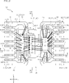
- FIG. FIG. 2 is a plan view corresponding to FIG. 1 and seen through the sealing resin
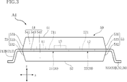
- 3 is a front view of the semiconductor device shown in FIG. 1.
- FIG. 4 is a left side view of the semiconductor device shown in FIG. 1.
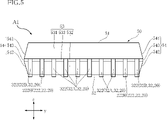
- FIG. 5 is a right side view of the semiconductor device shown in FIG. 1.
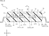
- FIG. 6 is a cross-sectional view taken along line VI-VI of FIG.
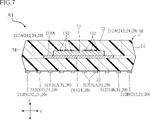
- FIG. 7 is a cross-sectional view along line VII-VII of FIG. 8 is a partially enlarged view of FIG. 2.
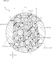
- FIG. 9 is a cross-sectional view along line IX-IX in FIG. 8.
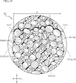
- FIG. 10 is a partially enlarged view of FIG. 6.
- FIG. 11 is a plan view of the semiconductor device according to the second embodiment of the present disclosure, which is transparent through the sealing resin.
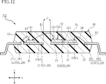
- 12 is a cross-sectional view taken along line XII-XII
- the semiconductor device A1 includes a first semiconductor element 11, a second semiconductor element 12, an insulating element 13, a plurality of conductive members 20, a plurality of first wires 41, a plurality of second wires 42, a plurality of third wires 43, a plurality of A fourth wire 44 , a plurality of fifth wires 45 , a plurality of sixth wires 46 and a sealing resin 50 are provided.
- the multiple conductive members 20 include a first member 21 , a second member 22 , multiple first terminals 31 , and multiple second terminals 32 .
- the semiconductor device A1 is surface-mounted, for example, on a wiring board of an inverter device such as an electric vehicle or a hybrid vehicle.
- the package format of the semiconductor device A1 is SOP (Small Outline Package).
- SOP Small Outline Package
- the package format of the semiconductor device A1 is not limited to SOP.
- FIG. 2 is transparent through the sealing resin 50 for convenience of understanding.
- the permeated sealing resin 50 is indicated by an imaginary line (chain double-dashed line).
- the thickness direction of each of the first semiconductor element 11 and the second semiconductor element 12 is called “thickness direction z”.
- a direction perpendicular to the thickness direction z is called a “first direction x”.
- a direction orthogonal to both the thickness direction z and the first direction x is called a "second direction y”.
- the first semiconductor element 11, the second semiconductor element 12, and the insulating element 13 are elements that serve as functional centers of the semiconductor device A1.
- the first semiconductor element 11, the second semiconductor element 12 and the insulating element 13 are composed of individual elements.
- the second semiconductor element 12 is located on the opposite side of the insulating element 13 from the first semiconductor element 11 .
- the first semiconductor element 11, the second semiconductor element 12, and the insulating element 13 have a rectangular shape with long sides in the second direction y.
- the first semiconductor element 11 is a gate driver controller (control element) that drives switching elements such as IGBTs and MOSFETs.
- the first semiconductor element 11 includes a circuit for converting a control signal input from an ECU or the like into a PWM control signal, a transmission circuit for transmitting the PWM control signal to the second semiconductor element 12, and a signal from the second semiconductor element 12. a receiving circuit for receiving an electrical signal of
- the second semiconductor element 12 is a gate driver (driving element) for driving the switching element.
- the second semiconductor element 12 includes a receiving circuit for receiving a PWM control signal, a circuit for driving the switching element based on the PWM control signal, and a transmitting circuit for transmitting an electrical signal to the first semiconductor element 11.
- the electric signal is, for example, an output signal from a temperature sensor arranged near the motor.
- the isolation element 13 is an element for transmitting the PWM control signal and other electrical signals in an isolated state.
- the insulating element 13 is of the inductive type.
- An example of the inductive insulating element 13 is an insulating transformer.
- An isolation transformer performs electrical signal transmission in an insulated state by inductively coupling two inductors (coils).
- the insulating element 13 has a substrate made of silicon.
- An inductor made of copper (Cu) is formed on the substrate.
- the inductor includes a transmitting inductor and a receiving inductor, which are stacked in the thickness direction z.
- a dielectric layer made of silicon dioxide (SiO 2 ) or the like is interposed between the transmitting side inductor and the receiving side inductor.
- the dielectric layer electrically insulates the transmitting inductor from the receiving inductor.
- the insulating element 13 may be of the capacitive type.
- a capacitor is an example of the capacitive insulating element 13 .
- the isolation element 13 may be a photocoupler.
- the voltage applied to the first semiconductor element 11 and the voltage applied to the second semiconductor element 12 are relatively different. Therefore, a potential difference is generated between the first semiconductor element 11 and the second semiconductor element 12 . Furthermore, in the semiconductor device A1, the power supply voltage supplied to the second semiconductor element 12 is higher than the power supply voltage supplied to the first semiconductor element 11. FIG.
- the first circuit including the first semiconductor element 11 as a component and the second circuit including the second semiconductor element 12 as a component are insulated from each other by the insulating element 13.
- Components of the first circuit include, in addition to the first semiconductor element 11, a first member 21, a plurality of first terminals 31, a plurality of first wires 41, a plurality of third wires 43, and a plurality of fifth wires 45.
- Components of the second circuit include, in addition to the second semiconductor element 12, a second member 22, a plurality of second terminals 32, a plurality of second wires 42, a plurality of fourth wires 44, and a plurality of sixth wires 46. including.
- the potentials of the first circuit and the second circuit are relatively different.
- the potential of the second circuit is higher than the potential of the first circuit.
- the isolation element 13 then relays mutual signals in the first and second circuits.
- the voltage applied to the ground of the first semiconductor element 11 is approximately 0 V
- the voltage applied to the ground of the second semiconductor element 12 is transiently 600 V. It may be more than that.
- the first semiconductor element 11 has a plurality of first electrodes 111.
- the plurality of first electrodes 111 are provided on the upper surface of the first semiconductor element 11 (the surface facing the same direction as the first mounting surface 211A of the first island portion 211 of the first member 21 described below).
- a composition of the plurality of first electrodes 111 includes, for example, aluminum (Al). In other words, each first electrode 111 contains aluminum.
- the multiple first electrodes 111 are electrically connected to the circuit configured in the first semiconductor element 11 .
- the insulating element 13 is positioned between the first semiconductor element 11 and the second semiconductor element 12 in the first direction x.
- a plurality of first relay electrodes 131 and a plurality of second relay electrodes 132 are provided on the upper surface of the insulating element 13 (the surface facing the same direction as the above-described first mounting surface 211A).
- Each of the plurality of first relay electrodes 131 and the plurality of second relay electrodes 132 is electrically connected to either the transmitting side inductor or the receiving side inductor.
- the plurality of first relay electrodes 131 are arranged along the second direction y and positioned closer to the first semiconductor element 11 than the second semiconductor element 12 in the first direction x.
- the plurality of second relay electrodes 132 are arranged along the second direction y and positioned closer to the second semiconductor element 12 than to the first semiconductor element 11 in the first direction x.
- the second semiconductor element 12 has multiple second electrodes 121 .
- the plurality of second electrodes 121 are provided on the upper surface of the second semiconductor element 12 (the surface facing the same direction as the second mounting surface 221A of the second island portion 221 of the second member 22 described below).
- the composition of the plurality of second electrodes 121 includes, for example, aluminum.
- the multiple second electrodes 121 are electrically connected to the circuit configured in the second semiconductor element 12 .
- the plurality of conductive members 20 form conductive paths between the first semiconductor element 11, the insulating element 13, the second semiconductor element 12, and the wiring board on which the semiconductor device A1 is mounted.
- a plurality of conductive members 20 are obtained from the same lead frame.
- the leadframe includes copper in its composition.
- the multiple conductive members 20 include the first member 21 , the second member 22 , the multiple first terminals 31 , and the multiple second terminals 32 .
- the first member 21 and the second member 22 are positioned apart from each other in the first direction x, as shown in FIGS.
- semiconductor device A1 first semiconductor element 11 and insulating element 13 are mounted on first member 21, and second semiconductor element 12 is mounted on second member 22.
- the voltage applied to the second member 22 is relatively different from the voltage applied to the first member 21 .
- the voltage applied to the second member 22 is higher than the voltage applied to the first member 21 .
- the first member 21 has a first island portion 211 and two first suspension lead portions 212 .
- the first island portion 211 has a first mounting surface 211A facing the thickness direction z.
- the semiconductor device A1 the first semiconductor element 11 and the insulating element 13 are mounted on the first mounting surface 211A.
- the first semiconductor element 11 and the insulating element 13 are bonded to the first mounting surface 211A via a conductive bonding material (solder, metal paste, etc.) (not shown).
- the first island portion 211 is covered with the sealing resin 50 .
- the thickness of first island portion 211 is, for example, 100 ⁇ m or more and 300 ⁇ m or less.
- the first island portion 211 has a plurality of through holes 213 formed therein.
- Each of the plurality of through holes 213 penetrates the first island portion 211 in the thickness direction z and extends along the second direction y.
- At least one of the plurality of through holes 213 is positioned between the first semiconductor element 11 and the insulating element 13 when viewed in the thickness direction z.
- the plurality of through holes 213 are arranged along the second direction y.
- the two first suspension lead portions 212 extend from both sides of the first island portion 211 in the second direction y.
- the two first suspension lead portions 212 are positioned apart from each other in the second direction y. At least one of the two first suspension lead portions 212 is electrically connected to the ground of the first semiconductor element 11 via the fifth wire 45 .
- Each of the two first hanging lead portions 212 has a covered portion 212A and an exposed portion 212B.
- the covering portion 212A is connected to the first island portion 211 and covered with the sealing resin 50 .
- the exposed portion 212B is connected to the covered portion 212A and exposed from the sealing resin 50 .
- the exposed portion 212B extends along the first direction x when viewed in the thickness direction z. As shown in FIG. 3, the exposed portion 212B is bent in a gull-wing shape when viewed in the second direction y.
- the surface of exposed portion 212B may be plated with tin (Sn), for example.
- the second member 22 has a second island portion 221 and two second suspension lead portions 222 .
- the second island portion 221 has a second mounting surface 221A facing the thickness direction z.
- the semiconductor device A1 the second semiconductor element 12 is mounted on the second mounting surface 221A.
- the second semiconductor element 12 is bonded to the second mounting surface 221A via a conductive bonding material (solder, metal paste, etc.) not shown.
- the second island portion 221 is covered with the sealing resin 50 .
- the thickness of second island portion 221 is, for example, 100 ⁇ m or more and 300 ⁇ m or less.
- the second island portion 221 overlaps the first island portion 211 of the first member 21 when viewed in the first direction x.
- the two second suspension lead portions 222 extend from both sides of the second island portion 221 in the second direction y.
- the two second suspension lead portions 222 are positioned apart from each other in the second direction y. At least one of the two second suspension lead portions 222 is electrically connected to the ground of the second semiconductor element 12 via the sixth wire 46 .
- Each of the two second suspension lead portions 222 has a covered portion 222A and an exposed portion 222B.
- the cover portion 222A is connected to the second island portion 221 and covered with the sealing resin 50 .
- the exposed portion 222B is connected to the covered portion 222A and is exposed from the sealing resin 50 .
- the exposed portion 222B extends along the first direction x when viewed in the thickness direction z. As shown in FIG. 3, the exposed portion 222B is bent in a gull-wing shape when viewed in the second direction y.
- the surface of the exposed portion 222B may be plated with tin, for example.
- the first island portion 211 of the first member 21 and the second island portion 221 of the second member 22 are separated from each other by a distance P in the first direction x.
- the spacing P is the minimum distance between the first island portion 211 and the second island portion 221 .
- the plurality of first terminals 31 are positioned on one side in the first direction x, as shown in FIGS. More specifically, the plurality of first terminals 31 are located on the side opposite to the second island portion 221 of the second member 22 with respect to the first island portion 211 of the first member 21 in the first direction x. .
- the multiple first terminals 31 are arranged along the second direction y. At least one of the plurality of first terminals 31 is electrically connected to the first semiconductor element 11 via the third wire 43 .
- the multiple first terminals 31 include multiple first intermediate terminals 31A and two first side terminals 31B.
- the two first side terminals 31B are located on both sides of the plurality of first intermediate terminals 31A in the second direction y. Each of the two first side terminals 31B is connected to either of the two first suspension lead portions 212 of the first member 21 in the second direction y and the first intermediate terminal located closest to the first suspension lead portion 212. 31A.
- the plurality of first terminals 31 have covered portions 311 and exposed portions 312 .
- the covering portion 311 is covered with the sealing resin 50 .
- the dimension of the covering portion 311 of each of the two first side terminals 31B in the first direction x is larger than the dimension of the covering portion 311 of each of the plurality of first intermediate terminals 31A in the first direction x.
- the covering portion 311 has a metal layer 33 .
- the metal layer 33 is positioned on one side of the covering portion 311 in the thickness direction z (the side facing the first mounting surface 211A of the first island portion 211 of the first member 21).
- the metal layer 33 is in contact with the sealing resin 50 .
- the composition of the metal layer 33 contains silver.
- the exposed portion 312 is connected to the covering portion 311 and exposed from the sealing resin 50 .
- the exposed portion 312 extends along the first direction x when viewed in the thickness direction z.
- the exposed portion 312 is bent in a gull-wing shape when viewed in the second direction y.
- the shape of the exposed portion 312 is equal to the shape of the exposed portion 212B of each of the two first hanging lead portions 212 of the first member 21 .
- the surface of the exposed portion 312 may be plated with tin, for example.
- the plurality of second terminals 32 are positioned on the other side in the first direction x, as shown in FIGS. More specifically, the plurality of second terminals 32 are located on the side opposite to the plurality of first terminals 31 with respect to the first island portion 211 of the first member 21 in the first direction x.
- the multiple second terminals 32 are arranged along the second direction y. At least one of the plurality of second terminals 32 is electrically connected to the second semiconductor element 12 via the fourth wire 44 .
- the multiple second terminals 32 include multiple second intermediate terminals 32A and two second side terminals 32B.
- the two second side terminals 32B are located on both sides of the plurality of second intermediate terminals 32A in the second direction y.
- Two second suspensions of the second member 22 are provided between one of the two second side terminals 32B and the second intermediate terminal 32A located closest to the second side terminal 32B in the second direction y. Any of the leads 222 is located.
- the plurality of second terminals 32 have covered portions 321 and exposed portions 322 .
- the covering portion 321 is covered with the sealing resin 50 .
- the dimension of the covering portion 321 of each of the two second side terminals 32B in the first direction x is larger than the dimension of the covering portion 321 of each of the plurality of second intermediate terminals 32A in the first direction x.
- the covering portion 321 has the metal layer 33 shown in FIG.
- the metal layer 33 is located on one side of the covering portion 321 in the thickness direction z (the side facing the second mounting surface 221A of the second island portion 221 of the second member 22).
- the metal layer 33 is in contact with the sealing resin 50 .
- the exposed portion 322 is connected to the covering portion 321 and exposed from the sealing resin 50 .
- the exposed portion 322 extends along the first direction x when viewed in the thickness direction z.
- the exposed portion 322 is bent in a gull-wing shape when viewed in the second direction y.
- the shape of the exposed portion 322 is equal to the shape of the exposed portion 222B of each of the two second suspension lead portions 222 of the second member 22 .
- the surface of the exposed portion 322 may be plated with tin, for example.
- each of the plurality of first wires 41 is connected to one of the plurality of first relay electrodes 131 of the insulating element 13 and one of the plurality of first electrodes 111 of the first semiconductor element 11. is joined to Thereby, the first semiconductor element 11 and the insulating element 13 are electrically connected to each other.
- the multiple first wires 41 are arranged along the second direction y.
- the composition of the plurality of first wires 41 contains gold (Au).
- each of the plurality of second wires 42 is connected to one of the plurality of second relay electrodes 132 of the insulating element 13 and one of the plurality of second electrodes 121 of the second semiconductor element 12. is joined to Thereby, the second semiconductor element 12 and the insulating element 13 are electrically connected to each other.
- the multiple second wires 42 are arranged along the second direction y. In the semiconductor device A ⁇ b>1 , the plurality of second wires 42 straddle between the first island portion 211 of the first member 21 and the second island portion 221 of the second member 22 .
- the composition of the plurality of second wires 42 includes gold.
- each of the plurality of third wires 43 is connected to one of the plurality of first electrodes 111 of the first semiconductor element 11 and one of the covering portions 311 of the plurality of first terminals 31. is joined to Accordingly, at least one of the plurality of first terminals 31 is electrically connected to the first semiconductor element 11 .
- the composition of the plurality of third wires 43 contains gold.
- the composition of the plurality of third wires 43 may contain copper.
- each of the plurality of fourth wires 44 is connected to one of the plurality of second electrodes 121 of the second semiconductor element 12 and the covering portion 321 of one of the plurality of second terminals 32. is joined to As a result, at least one of the plurality of second terminals 32 is electrically connected to the second semiconductor element 12 .
- the composition of the plurality of fourth wires 44 includes gold. Alternatively, the composition of the plurality of fourth wires 44 may contain copper.
- Each of the plurality of fifth wires 45 as shown in FIG. It is joined to the covering portion 212A. Thereby, the first semiconductor element 11 is electrically connected to the first member 21 .
- the composition of the plurality of fifth wires 45 includes gold.
- the composition of the plurality of fifth wires 45 may contain copper.
- Each of the plurality of sixth wires 46 is joined to the covering portion 222A. Thereby, the second semiconductor element 12 is electrically connected to the second member 22 .
- the composition of the plurality of sixth wires 46 includes gold. Alternatively, the composition of the plurality of sixth wires 46 may contain copper.
- the sealing resin 50 covers the first semiconductor element 11, the second semiconductor element 12, the insulating element 13, and a portion of each of the plurality of conductive members 20.
- the sealing resin 50 includes a plurality of first wires 41, a plurality of second wires 42, a plurality of third wires 43, a plurality of fourth wires 44, a plurality of fifth wires 45, and a plurality of sixth wires 46. covering.
- the sealing resin 50 has electrical insulation.
- the sealing resin 50 insulates the first member 21 and the second member 22 from each other.
- the sealing resin 50 contains a filler 50B.
- the filler 50B has electrical insulation.
- the sealing resin 50 has a rectangular shape when viewed in the thickness direction z.
- the sealing resin 50 has a top surface 51, a bottom surface 52, a pair of first side surfaces 53, and a pair of second side surfaces .
- top surface 51 and the bottom surface 52 are positioned apart from each other in the thickness direction z.
- the top surface 51 and the bottom surface 52 face opposite sides in the thickness direction z.
- Each of top surface 51 and bottom surface 52 is flat (or substantially flat).
- the pair of first side surfaces 53 are connected to the top surface 51 and the bottom surface 52 and are separated from each other in the first direction x.
- the exposed portions 212B of the two first hanging lead portions 212 of the first member 21, the plurality of first terminals 31 and the exposed portion 312 of are exposed.
- the exposed portions 222B of the two second suspension lead portions 222 of the second member 22, the plurality of second terminals 32 and the exposed portion 322 of are exposed.
- Each of the pair of first side surfaces 53 includes a first upper portion 531, a first lower portion 532 and a first intermediate portion 533, as shown in FIGS.
- One side of the first upper portion 531 in the thickness direction z is connected to the top surface 51 , and the other side in the thickness direction z is connected to the first intermediate portion 533 .
- the first upper portion 531 is inclined with respect to the top surface 51 .
- One side of the first lower portion 532 in the thickness direction z is connected to the bottom surface 52 , and the other side in the thickness direction z is connected to the first intermediate portion 533 .
- the first lower portion 532 is inclined with respect to the bottom surface 52 .
- first intermediate portion 533 in the thickness direction z is connected to the first upper portion 531 , and the other side in the thickness direction z is connected to the first lower portion 532 .
- the in-plane directions of the first intermediate portion 533 are the thickness direction z and the second direction y.
- the first intermediate portion 533 is located outside the top surface 51 and the bottom surface 52 when viewed in the thickness direction z. From the first intermediate portions 533 of the pair of first side surfaces 53, the exposed portions 212B of the two first suspension lead portions 212 of the first member 21 and the exposed portions 222B of the two second suspension lead portions 222 of the second member 22 are exposed. , the exposed portions 312 of the plurality of first terminals 31 and the exposed portions 322 of the plurality of second terminals 32 are exposed.
- the pair of second side surfaces 54 are connected to the top surface 51 and the bottom surface 52 and are separated from each other in the second direction y. As shown in FIG. 1 , the first member 21 , the second member 22 , the plurality of first terminals 31 , and the plurality of second terminals 32 are positioned away from the pair of second side surfaces 54 .
- each of the pair of second side surfaces 54 includes a second upper portion 541, a second lower portion 542 and a second intermediate portion 543.
- One side of the second upper portion 541 in the thickness direction z is connected to the top surface 51 , and the other side in the thickness direction z is connected to the second intermediate portion 543 .
- the second upper portion 541 is inclined with respect to the top surface 51 .
- One side of the second lower portion 542 in the thickness direction z is connected to the bottom surface 52 , and the other side in the thickness direction z is connected to the second intermediate portion 543 .
- the second lower portion 542 is inclined with respect to the bottom surface 52 .
- the second intermediate portion 543 has one side in the thickness direction z connected to the second upper portion 541 and the other side in the thickness direction z connected to the second lower portion 542 .
- the in-plane directions of the second intermediate portion 543 are the thickness direction z and the second direction y.
- the second intermediate portion 543 is located outside the top surface 51 and the bottom surface 52 when viewed in the thickness direction z.
- the sealing resin 50 includes a base material 50A and a filler 50B.
- Base material 50A mainly contains an epoxy resin and a curing agent.
- the composition of filler 50B includes silicon dioxide.
- the weight percentage of the filler 50B is about 90% of the sealing resin 50.
- a square cross section S assumed in the sealing resin 50 shown in FIG. 9 contains at least eight or more fillers 50B each having a particle size D equal to or larger than a reference value.
- the particle diameter D is the maximum diameter of each filler 50B in the square section S.
- the filler 50B whose particle size D is equal to or greater than the reference value is indicated by oblique lines.
- the square section S traverses only the sealing resin 50 .
- the position of the square section S in the sealing resin 50 is not limited.
- the length of one side of the square section S and the reference value of the particle diameter D of the filler 50B are defined by the minimum spacing Pmin shown in FIG.
- the minimum distance Pmin is the minimum distance between two adjacent conductive members 20 among the plurality of conductive members 20 .
- the minimum spacing Pmin is the minimum spacing between two adjacent first terminals 31 in the second direction y and the minimum spacing between two adjacent second terminals 32 in the second direction y. whichever is smaller. In the semiconductor device A1, the minimum spacing Pmin is 150 ⁇ m.
- the length of one side of the assumed square cross section S in the sealing resin 50 is equal to 2 ⁇ 3 of the minimum interval Pmin. In the semiconductor device A1, the length of one side of the square section S is 100 ⁇ m.
- a reference value for the particle size D of the filler 50B is equal to 1 ⁇ 8 of the minimum spacing Pmin. In the semiconductor device A1, the reference value of the grain size D is 18.75 ⁇ m. Therefore, in the semiconductor device A1, it can be said that at least eight or more fillers 50B each having a particle size D of 18.75 ⁇ m or more are included in the square section S having a side length of 100 ⁇ m. Furthermore, the maximum value of the particle diameter D of the filler 50B is 1/2 of the minimum spacing Pmin. Therefore, in the semiconductor device A1, the maximum value of the particle size D of the filler 50B is 75 ⁇ m.
- the particle size distribution of the filler 50B contained in the square cross section S is uniform in the sealing resin 50 as shown in FIG. Further, the distance P between the first member 21 (first island portion 211) and the second member 22 (second island portion 221) shown in FIG. 10 is 1.0 times or more and 3.0 times or less of the minimum distance Pmin. .
- a half-bridge circuit including a low-side (low-potential side) switching element and a high-side (high-potential side) switching element.
- these switching elements are MOSFETs.
- the low-side switching element both the source of the switching element and the reference potential of the gate driver that drives the switching element are grounded.
- both the reference potential of the source of the switching element and the reference potential of the gate driver that drives the switching element correspond to the potential at the output node of the half bridge circuit.
- the reference potential of the gate driver that drives the high-side switching element changes.
- the reference potential is equivalent to the voltage applied to the drain of the high-side switching element (for example, 600V or higher).
- the semiconductor device A1 the ground of the first semiconductor element 11 and the ground of the second semiconductor element 12 are separated. Therefore, when the semiconductor device A1 is used as a gate driver for driving the high-side switching element, a transient voltage equivalent to the voltage applied to the drain of the high-side switching element is applied to the ground of the second semiconductor element 12. applied
- the semiconductor device A1 includes a plurality of conductive members 20 including first members 21 and second members 22, and a sealing resin 50 covering a portion of each of the plurality of conductive members 20.
- the voltage applied to the second member 22 is relatively different from the voltage applied to the first member 21 .
- the sealing resin 50 contains a filler 50B having electrical insulation.
- a square cross section S of the sealing resin 50 having a side length of 2/3 of the minimum interval Pmin between two adjacent conductive members 20 among the plurality of conductive members 20 has a particle diameter D of each of the minimum intervals Pmin.
- the semiconductor device A1 breaks down, it is confirmed that the breakdown occurs at the interface 50C between the base material 50A of the sealing resin 50 shown in FIG. 9 and the filler 50B. Furthermore, when the semiconductor device A1 breaks down, the probability of breakdown in the sealing resin 50 filling the gap P between the first member 21 and the second member 22 to which the voltages applied are relatively different is extremely high. Dielectric breakdown occurs when charged carriers move from one conductive member 20 to the other conductive member 20 via the sealing resin 50 embedded between two adjacent conductive members 20 . The carrier moves in the sealing resin 50 along the interface 50C between the base material 50A and the filler 50B. Therefore, by adopting the above-described configuration of the semiconductor device A1, as shown in FIG. ), the moving distance L of the carrier to reach the first mounting surface 211A becomes longer. As a result, the time required for dielectric breakdown of the semiconductor device A1 increases. Therefore, according to the semiconductor device A1, it is possible to further improve the withstand voltage.
- the length of one side of the square section S of the sealing resin 50 and the reference value of the particle size D of the filler 50B of the sealing resin 50 are determined by the minimum distance Pmin between two adjacent conductive members 20 among the plurality of conductive members 20. Defined. As a result, the fillers 50B that do not contribute to the improvement of the withstand voltage of the semiconductor device A1 are excluded from the fillers 50B having the particle size D equal to or larger than the reference value. can be excluded. Furthermore, the maximum value of the particle diameter D of the filler 50B is 1/2 of the minimum spacing Pmin. As a result, in the manufacture of the semiconductor device A1, the fluidized sealing resin 50 smoothly passes between the two adjacent conductive members 20, so that the filling failure of the sealing resin 50 can be prevented.
- the distance P between the first member 21 and the second member 22 is important in further improving the withstand voltage of the semiconductor device A1.
- the interval P is preferably 1.0 to 3.0 times the minimum interval Pmin between two adjacent conductive members 20 among the plurality of conductive members 20 . If the interval P exceeds 3.0 times the minimum interval Pmin, although this contributes to the further improvement of the dielectric strength of the semiconductor device A1, it causes an increase in the size of the semiconductor device A1, which is not preferable.
- each of the plurality of conductive members 20 is exposed from one of the pair of first side surfaces 53 of the sealing resin 50 .
- the two first suspension lead portions 212 of the first member 21 are exposed from one side of the sealing resin 50 in the first direction x, and the two second suspension lead portions 222 of the second member 22 are sealed. It is obtained by exposing the stopper resin 50 from the other side in the first direction x.
- the plurality of conductive members 20 are positioned apart from the pair of second side surfaces 54 of the sealing resin 50 . Accordingly, in the semiconductor device A1, metal members such as island supports are not exposed from the pair of second side surfaces 54. As shown in FIG. Therefore, it is possible to improve the withstand voltage of the semiconductor device A1.
- a plurality of through holes 213 are formed in the first island portion 211 of the first member 21, which has a larger area than the second island portion 221 of the second member 22.
- the fluidized sealing resin 50 passes through the plurality of through-holes 213 in the manufacture of the semiconductor device A1, so that filling defects of the sealing resin 50 can be prevented. Therefore, it is possible to effectively suppress the formation of voids in the sealing resin 50 . This contributes to suppressing a decrease in the breakdown voltage of the semiconductor device A1.
- the semiconductor device A1 further includes a first wire 41 and a second wire 42.
- the first wire 41 is joined to the insulating element 13 and the first semiconductor element 11 .
- a second wire 42 is joined to the insulating element 13 and the second semiconductor element 12 .
- the composition of the first wire 41 and the second wire 42 contains gold.
- the first junction of the first wire 41 is formed on the first relay electrode 131 of the insulating element 13 , and the plurality of first terminals 31 and the first member Form the final joint of the first wire 41 on either of the two first suspension leads 212 of 21 .
- the first wire 41 has a shape in which the distance between the top portion of the first wire 41 closest to the top surface 51 of the sealing resin 50 and the insulating element 13 in the thickness direction z is ensured as long as possible. be able to.
- the first joint of the second wire 42 is formed on the second relay electrode 132 of the insulating element 13 , and the plurality of second terminals 32 and the second member 22 are formed. form the final joint on either of the two second suspension leads 222 of the .
- the second wire 42 can have a shape in which the distance between the top portion of the second wire 42 located closest to the top surface 51 and the insulating element 13 is ensured as long as possible in the thickness direction z. . This contributes to further improvement of the withstand voltage of the semiconductor device A1.
- FIG. 11 is transparent through the sealing resin 50 for convenience of understanding.
- the permeated sealing resin 50 is indicated by imaginary lines.
- the mounting form of the insulating element 13 is different from the above-described configuration of the semiconductor device A1.
- the insulating element 13 is mounted on the second mounting surface 221A of the second island portion 221 of the second member 22. As shown in FIGS. Therefore, in the semiconductor device A ⁇ b>2 , the plurality of first wires 41 straddle the first island portion 211 of the first member 21 and the second island portion 221 of the second member 22 . Thus, even if the potential of the second island portion 221 is higher than the potential of the first island portion 211 , the insulating element 13 can be mounted on the second island portion 221 .
- the semiconductor device A2 includes a plurality of conductive members 20 including a first member 21 and a second member 22, and a sealing resin 50 covering a portion of each of the plurality of conductive members 20.
- the voltage applied to the second member 22 is relatively different from the voltage applied to the first member 21 .
- the sealing resin 50 contains a filler 50B having electrical insulation.
- a square cross section S of the sealing resin 50 having a side length of 2/3 of the minimum interval Pmin between two adjacent conductive members 20 among the plurality of conductive members 20 has a particle diameter D of each of the minimum intervals Pmin.
- the semiconductor device A2 has the same effect as the semiconductor device A1 by adopting a configuration common to the semiconductor device A1.
- Appendix 1 a plurality of conductive members including a first member and a second member; a first semiconductor element electrically connected to one of the plurality of conductive members; a second semiconductor element that is electrically connected to any one of the plurality of conductive members and to which a voltage relatively different from the voltage applied to the first semiconductor element is applied; a sealing resin covering a part of each of the plurality of conductive members, the first semiconductor element and the second semiconductor element; the voltage applied to the second member is relatively different from the voltage applied to the first member;
- the sealing resin contains an electrically insulating filler, Assuming that the sealing resin has a square cross section with a side length equal to 2/3 of the minimum distance between two adjacent conductive members among the plurality of conductive members,
- the semiconductor device wherein the square cross section contains at least 8 pieces of at least a portion of the filler, each of which has a grain size of 1/8 or more of the minimum spacing.
- Appendix 2 The semiconductor device according to appendix 1, wherein the maximum particle size of the filler is 1/2 of the minimum spacing.
- Appendix 3. the first member and the second member are separated from each other in a first direction perpendicular to the thickness direction of each of the first semiconductor element and the second semiconductor element; The first semiconductor element is mounted on the first member, The second semiconductor element is mounted on the second member, The semiconductor device according to appendix 2, wherein the distance between the first member and the second member is 1.0 to 3.0 times the minimum distance.
- Appendix 4. The semiconductor device according to appendix 3, wherein the first semiconductor element is electrically connected to the first member.
- Appendix 5. The semiconductor device according to appendix 4, wherein the second semiconductor element is electrically connected to the second member.
- the plurality of conductive members includes a plurality of first terminals positioned on one side in the first direction and a plurality of second terminals positioned on the other side in the first direction,
- the first semiconductor element is electrically connected to the plurality of first terminals, 6.
- Appendix 7. The semiconductor device according to appendix 6, wherein the plurality of first terminals and the plurality of second terminals are arranged along a second direction orthogonal to the first direction. Appendix 8.
- the first member has a first island portion on which the first semiconductor element is mounted, and two first hanging lead portions connected to both sides of the first island portion in the second direction, The semiconductor device according to appendix 7, wherein the two first suspension lead portions are exposed from one side of the sealing resin in the first direction.
- the second member has a second island portion on which the second semiconductor element is mounted, and two second hanging lead portions connected to both sides of the second island portion in the second direction, The semiconductor device according to appendix 8, wherein the two second suspension lead portions are exposed from the other side of the sealing resin in the first direction.
- Appendix 10 The semiconductor device according to appendix 9, wherein the second island portion overlaps the first island portion when viewed in the first direction. Appendix 11. 11.
Landscapes
- Structures Or Materials For Encapsulating Or Coating Semiconductor Devices Or Solid State Devices (AREA)
Abstract
Description
付記1.
第1部材および第2部材を含む複数の導電部材と、
前記複数の導電部材のいずれかに導通する第1半導体素子と、
前記複数の導電部材のいずれかに導通するとともに、前記第1半導体素子に印加される電圧と相対的に異なる電圧が印加される第2半導体素子と、
前記複数の導電部材の各々の一部、前記第1半導体素子および前記第2半導体素子を覆う封止樹脂と、を備え、
前記第2部材に印加される電圧は、前記第1部材に印加される電圧と相対的に異なり、
前記封止樹脂には、電気絶縁性を有するフィラーが含有されており、
前記複数の導電部材のうち隣り合う2つの前記導電部材の最小間隔の2/3に等しい一辺の長さを有する正方形断面を前記封止樹脂において仮定した場合、
前記正方形断面には、各々の粒径が前記最小間隔の1/8以上である前記フィラーの少なくとも一部が8個以上含まれている、半導体装置。
付記2.
前記フィラーの粒径の最大値は、前記最小間隔の1/2である、付記1に記載の半導体装置。
付記3.
前記第1部材および前記第2部材は、前記第1半導体素子および前記第2半導体素子の各々の厚さ方向に対して直交する第1方向において互いに離れて位置しており、
前記第1半導体素子は、前記第1部材に搭載されており、
前記第2半導体素子は、前記第2部材に搭載されており、
前記第1部材と前記第2部材の間隔は、前記最小間隔の1.0倍以上3.0倍以下である、付記2に記載の半導体装置。
付記4.
前記第1半導体素子は、前記第1部材に導通している、付記3に記載の半導体装置。
付記5.
前記第2半導体素子は、前記第2部材に導通している、付記4に記載の半導体装置。
付記6.
前記複数の導電部材は、前記第1方向の一方側に位置する複数の第1端子と、前記第1方向の他方側に位置する複数の第2端子と、を含み、
前記第1半導体素子は、前記複数の第1端子に導通しており、
前記第2半導体素子は、前記複数の第2端子に導通している、付記3ないし5のいずれかに記載の半導体装置。
付記7.
前記複数の第1端子と、前記複数の第2端子と、は、それぞれ前記第1方向に対して直交する第2方向に沿って配列されている、付記6に記載の半導体装置。
付記8.
前記第1部材は、前記第1半導体素子が搭載された第1アイランド部と、前記第1アイランド部の前記第2方向の両側につながる2つの第1吊リード部と、を有し、
前記2つの第1吊リード部は、前記封止樹脂の前記第1方向の一方側から露出している、付記7に記載の半導体装置。
付記9.
前記第2部材は、前記第2半導体素子が搭載された第2アイランド部と、前記第2アイランド部の前記第2方向の両側につながる2つの第2吊リード部と、を有し、
前記2つの第2吊リード部は、前記封止樹脂の前記第1方向の他方側から露出している、付記8に記載の半導体装置。
付記10.
前記第1方向に視て、前記第2アイランド部は、前記第1アイランド部に重なっている、付記9に記載の半導体装置。
付記11.
前記第2部材に印加される電圧は、前記第1部材に印加される電圧よりも高い、付記3ないし10のいずれかに記載の半導体装置。
付記12.
前記第1半導体素子と前記第2半導体素子との相互信号を中継し、かつ前記第1半導体素子および前記第2半導体素子を互いに絶縁する絶縁素子をさらに備え、
前記絶縁素子は、インダクティブ型である、付記3ないし11のいずれかに記載の半導体装置。
付記13.
前記絶縁素子は、前記第1部材に搭載されている、付記12に記載の半導体装置。
付記14.
前記絶縁素子は、前記第2部材に搭載されている、付記12に記載の半導体装置。
付記15.
第1ワイヤおよび第2ワイヤをさらに備え、
前記第1ワイヤは、前記絶縁素子および前記第1半導体素子に接合されており、
前記第2ワイヤは、前記絶縁素子および前記第2半導体素子に接合されており、
前記第1ワイヤおよび前記第2ワイヤの組成は、金を含む、付記12ないし14のいずれかに記載の半導体装置。
付記16.
前記フィラーの組成は、二酸化ケイ素を含む、付記1ないし15のいずれかに記載の半導体装置。
111:第1電極 12:第2半導体素子
121:第2電極 13:絶縁素子
131:第1中継電極 132:第2中継電極
20:導電部材 21:第1部材
211:第1アイランド部 211A:第1搭載面
212:第1吊リード部 212A:被覆部
212B:露出部 213:貫通孔
22:第2部材 221:第2アイランド部
221A:第2搭載面 222:第2吊リード部
222A:被覆部 222B:露出部
31:第1端子 31A:第1中間端子
31B:第1側端子 311:被覆部
312:露出部 32:第2端子
32A:第2中間端子 32B:第2側端子
321:被覆部 322:露出部
33:金属層 41:第1ワイヤ
42:第2ワイヤ 43:第3ワイヤ
44:第4ワイヤ 45:第5ワイヤ
46:第6ワイヤ 50:封止樹脂
50A:基材 50B:フィラー
50C:界面 51:頂面
52:底面 53:第1側面
531:第1上部 532:第1下部
533:第1中間部 54:第2側面
541:第2上部 542:第2下部
543:第2中間部 Pmin:最小間隔
D:粒径 S:正方形断面
P:間隔 z:厚さ方向
x:第1方向 y:第2方向
Claims (16)
- 第1部材および第2部材を含む複数の導電部材と、
前記複数の導電部材のいずれかに導通する第1半導体素子と、
前記複数の導電部材のいずれかに導通するとともに、前記第1半導体素子に印加される電圧と相対的に異なる電圧が印加される第2半導体素子と、
前記複数の導電部材の各々の一部、前記第1半導体素子および前記第2半導体素子を覆う封止樹脂と、を備え、
前記第2部材に印加される電圧は、前記第1部材に印加される電圧と相対的に異なり、
前記封止樹脂には、電気絶縁性を有するフィラーが含有されており、
前記複数の導電部材のうち隣り合う2つの前記導電部材の最小間隔の2/3に等しい一辺の長さを有する正方形断面を前記封止樹脂において仮定した場合、
前記正方形断面には、各々の粒径が前記最小間隔の1/8以上である前記フィラーの少なくとも一部が8個以上含まれている、半導体装置。 - 前記フィラーの粒径の最大値は、前記最小間隔の1/2である、請求項1に記載の半導体装置。
- 前記第1部材および前記第2部材は、前記第1半導体素子および前記第2半導体素子の各々の厚さ方向に対して直交する第1方向において互いに離れて位置しており、
前記第1半導体素子は、前記第1部材に搭載されており、
前記第2半導体素子は、前記第2部材に搭載されており、
前記第1部材と前記第2部材の間隔は、前記最小間隔の1.0倍以上3.0倍以下である、請求項2に記載の半導体装置。 - 前記第1半導体素子は、前記第1部材に導通している、請求項3に記載の半導体装置。
- 前記第2半導体素子は、前記第2部材に導通している、請求項4に記載の半導体装置。
- 前記複数の導電部材は、前記第1方向の一方側に位置する複数の第1端子と、前記第1方向の他方側に位置する複数の第2端子と、を含み、
前記第1半導体素子は、前記複数の第1端子に導通しており、
前記第2半導体素子は、前記複数の第2端子に導通している、請求項3ないし5のいずれかに記載の半導体装置。 - 前記複数の第1端子と、前記複数の第2端子と、は、それぞれ前記第1方向に対して直交する第2方向に沿って配列されている、請求項6に記載の半導体装置。
- 前記第1部材は、前記第1半導体素子が搭載された第1アイランド部と、前記第1アイランド部の前記第2方向の両側につながる2つの第1吊リード部と、を有し、
前記2つの第1吊リード部は、前記封止樹脂の前記第1方向の一方側から露出している、請求項7に記載の半導体装置。 - 前記第2部材は、前記第2半導体素子が搭載された第2アイランド部と、前記第2アイランド部の前記第2方向の両側につながる2つの第2吊リード部と、を有し、
前記2つの第2吊リード部は、前記封止樹脂の前記第1方向の他方側から露出している、請求項8に記載の半導体装置。 - 前記第1方向に視て、前記第2アイランド部は、前記第1アイランド部に重なっている、請求項9に記載の半導体装置。
- 前記第2部材に印加される電圧は、前記第1部材に印加される電圧よりも高い、請求項3ないし10のいずれかに記載の半導体装置。
- 前記第1半導体素子と前記第2半導体素子との相互信号を中継し、かつ前記第1半導体素子および前記第2半導体素子を互いに絶縁する絶縁素子をさらに備え、
前記絶縁素子は、インダクティブ型である、請求項3ないし11のいずれかに記載の半導体装置。 - 前記絶縁素子は、前記第1部材に搭載されている、請求項12に記載の半導体装置。
- 前記絶縁素子は、前記第2部材に搭載されている、請求項12に記載の半導体装置。
- 第1ワイヤおよび第2ワイヤをさらに備え、
前記第1ワイヤは、前記絶縁素子および前記第1半導体素子に接合されており、
前記第2ワイヤは、前記絶縁素子および前記第2半導体素子に接合されており、
前記第1ワイヤおよび前記第2ワイヤの組成は、金を含む、請求項12ないし14のいずれかに記載の半導体装置。 - 前記フィラーの組成は、二酸化ケイ素を含む、請求項1ないし15のいずれかに記載の半導体装置。
Priority Applications (5)
| Application Number | Priority Date | Filing Date | Title |
|---|---|---|---|
| DE112022000972.1T DE112022000972T5 (de) | 2021-03-19 | 2022-02-25 | Halbleiterbauelement |
| JP2023506914A JP7791168B2 (ja) | 2021-03-19 | 2022-02-25 | 半導体装置 |
| CN202280022315.9A CN116998006A (zh) | 2021-03-19 | 2022-02-25 | 半导体器件 |
| US18/465,558 US20240006274A1 (en) | 2021-03-19 | 2023-09-12 | Semiconductor device |
| JP2025245462A JP2026041996A (ja) | 2021-03-19 | 2025-12-11 | 半導体装置 |
Applications Claiming Priority (2)
| Application Number | Priority Date | Filing Date | Title |
|---|---|---|---|
| JP2021045491 | 2021-03-19 | ||
| JP2021-045491 | 2021-03-19 |
Related Child Applications (1)
| Application Number | Title | Priority Date | Filing Date |
|---|---|---|---|
| US18/465,558 Continuation US20240006274A1 (en) | 2021-03-19 | 2023-09-12 | Semiconductor device |
Publications (1)
| Publication Number | Publication Date |
|---|---|
| WO2022196294A1 true WO2022196294A1 (ja) | 2022-09-22 |
Family
ID=83322272
Family Applications (1)
| Application Number | Title | Priority Date | Filing Date |
|---|---|---|---|
| PCT/JP2022/007924 Ceased WO2022196294A1 (ja) | 2021-03-19 | 2022-02-25 | 半導体装置 |
Country Status (5)
| Country | Link |
|---|---|
| US (1) | US20240006274A1 (ja) |
| JP (2) | JP7791168B2 (ja) |
| CN (1) | CN116998006A (ja) |
| DE (1) | DE112022000972T5 (ja) |
| WO (1) | WO2022196294A1 (ja) |
Citations (2)
| Publication number | Priority date | Publication date | Assignee | Title |
|---|---|---|---|---|
| US20140239472A1 (en) * | 2013-02-28 | 2014-08-28 | Frank Tim Jones | Dual-flag stacked die package |
| JP2016207714A (ja) * | 2015-04-16 | 2016-12-08 | ローム株式会社 | 半導体装置 |
Family Cites Families (1)
| Publication number | Priority date | Publication date | Assignee | Title |
|---|---|---|---|---|
| JP5767294B2 (ja) | 2013-10-07 | 2015-08-19 | ルネサスエレクトロニクス株式会社 | 半導体装置 |
-
2022
- 2022-02-25 WO PCT/JP2022/007924 patent/WO2022196294A1/ja not_active Ceased
- 2022-02-25 CN CN202280022315.9A patent/CN116998006A/zh active Pending
- 2022-02-25 JP JP2023506914A patent/JP7791168B2/ja active Active
- 2022-02-25 DE DE112022000972.1T patent/DE112022000972T5/de active Granted
-
2023
- 2023-09-12 US US18/465,558 patent/US20240006274A1/en active Pending
-
2025
- 2025-12-11 JP JP2025245462A patent/JP2026041996A/ja active Pending
Patent Citations (2)
| Publication number | Priority date | Publication date | Assignee | Title |
|---|---|---|---|---|
| US20140239472A1 (en) * | 2013-02-28 | 2014-08-28 | Frank Tim Jones | Dual-flag stacked die package |
| JP2016207714A (ja) * | 2015-04-16 | 2016-12-08 | ローム株式会社 | 半導体装置 |
Also Published As
| Publication number | Publication date |
|---|---|
| DE112022000972T5 (de) | 2023-11-23 |
| CN116998006A (zh) | 2023-11-03 |
| JPWO2022196294A1 (ja) | 2022-09-22 |
| JP2026041996A (ja) | 2026-03-10 |
| JP7791168B2 (ja) | 2025-12-23 |
| US20240006274A1 (en) | 2024-01-04 |
Similar Documents
| Publication | Publication Date | Title |
|---|---|---|
| US10985110B2 (en) | Semiconductor package having an electromagnetic shielding structure and method for producing the same | |
| US20240014107A1 (en) | Semiconductor device | |
| NL2021292B1 (en) | Electronic module | |
| US20240312877A1 (en) | Semiconductor device | |
| US20240047438A1 (en) | Semiconductor equipment | |
| JP7791168B2 (ja) | 半導体装置 | |
| US12616040B2 (en) | Metal layer plated to inner leads of a leadframe | |
| WO2022220013A1 (ja) | 半導体装置 | |
| US20240030109A1 (en) | Semiconductor device | |
| US20250070076A1 (en) | Semiconductor device | |
| US20250006775A1 (en) | Semiconductor element and semiconductor device | |
| US20250309068A1 (en) | Semiconductor device | |
| US20260096448A1 (en) | Semiconductor device | |
| WO2023095745A1 (ja) | 半導体装置 | |
| US20260018562A1 (en) | Semiconductor device | |
| US20260018498A1 (en) | Semiconductor device | |
| WO2022176690A1 (ja) | 半導体装置、半導体装置の設計方法および半導体装置の製造方法 | |
| US20230402353A1 (en) | Semiconductor device | |
| WO2022168606A1 (ja) | 半導体装置 |
Legal Events
| Date | Code | Title | Description |
|---|---|---|---|
| 121 | Ep: the epo has been informed by wipo that ep was designated in this application |
Ref document number: 22771050 Country of ref document: EP Kind code of ref document: A1 |
|
| ENP | Entry into the national phase |
Ref document number: 2023506914 Country of ref document: JP Kind code of ref document: A |
|
| WWE | Wipo information: entry into national phase |
Ref document number: 202280022315.9 Country of ref document: CN |
|
| WWE | Wipo information: entry into national phase |
Ref document number: 112022000972 Country of ref document: DE |
|
| 122 | Ep: pct application non-entry in european phase |
Ref document number: 22771050 Country of ref document: EP Kind code of ref document: A1 |