WO2022190817A1 - 強誘電性薄膜の形成方法、それを備える半導体装置 - Google Patents
強誘電性薄膜の形成方法、それを備える半導体装置 Download PDFInfo
- Publication number
- WO2022190817A1 WO2022190817A1 PCT/JP2022/006613 JP2022006613W WO2022190817A1 WO 2022190817 A1 WO2022190817 A1 WO 2022190817A1 JP 2022006613 W JP2022006613 W JP 2022006613W WO 2022190817 A1 WO2022190817 A1 WO 2022190817A1
- Authority
- WO
- WIPO (PCT)
- Prior art keywords
- semiconductor device
- thin film
- substrate
- ferroelectric thin
- hfn
- Prior art date
- Legal status (The legal status is an assumption and is not a legal conclusion. Google has not performed a legal analysis and makes no representation as to the accuracy of the status listed.)
- Ceased
Links
Images





Classifications
-
- C—CHEMISTRY; METALLURGY
- C23—COATING METALLIC MATERIAL; COATING MATERIAL WITH METALLIC MATERIAL; CHEMICAL SURFACE TREATMENT; DIFFUSION TREATMENT OF METALLIC MATERIAL; COATING BY VACUUM EVAPORATION, BY SPUTTERING, BY ION IMPLANTATION OR BY CHEMICAL VAPOUR DEPOSITION, IN GENERAL; INHIBITING CORROSION OF METALLIC MATERIAL OR INCRUSTATION IN GENERAL
- C23C—COATING METALLIC MATERIAL; COATING MATERIAL WITH METALLIC MATERIAL; SURFACE TREATMENT OF METALLIC MATERIAL BY DIFFUSION INTO THE SURFACE, BY CHEMICAL CONVERSION OR SUBSTITUTION; COATING BY VACUUM EVAPORATION, BY SPUTTERING, BY ION IMPLANTATION OR BY CHEMICAL VAPOUR DEPOSITION, IN GENERAL
- C23C16/00—Chemical coating by decomposition of gaseous compounds, without leaving reaction products of surface material in the coating, i.e. chemical vapour deposition [CVD] processes
- C23C16/22—Chemical coating by decomposition of gaseous compounds, without leaving reaction products of surface material in the coating, i.e. chemical vapour deposition [CVD] processes characterised by the deposition of inorganic material, other than metallic material
- C23C16/30—Deposition of compounds, mixtures or solid solutions, e.g. borides, carbides, nitrides
- C23C16/34—Nitrides
-
- H—ELECTRICITY
- H10—SEMICONDUCTOR DEVICES; ELECTRIC SOLID-STATE DEVICES NOT OTHERWISE PROVIDED FOR
- H10B—ELECTRONIC MEMORY DEVICES
- H10B51/00—Ferroelectric RAM [FeRAM] devices comprising ferroelectric memory transistors
- H10B51/30—Ferroelectric RAM [FeRAM] devices comprising ferroelectric memory transistors characterised by the memory core region
-
- H—ELECTRICITY
- H10—SEMICONDUCTOR DEVICES; ELECTRIC SOLID-STATE DEVICES NOT OTHERWISE PROVIDED FOR
- H10D—INORGANIC ELECTRIC SEMICONDUCTOR DEVICES
- H10D30/00—Field-effect transistors [FET]
- H10D30/01—Manufacture or treatment
- H10D30/021—Manufacture or treatment of FETs having insulated gates [IGFET]
-
- H—ELECTRICITY
- H10—SEMICONDUCTOR DEVICES; ELECTRIC SOLID-STATE DEVICES NOT OTHERWISE PROVIDED FOR
- H10D—INORGANIC ELECTRIC SEMICONDUCTOR DEVICES
- H10D30/00—Field-effect transistors [FET]
- H10D30/01—Manufacture or treatment
- H10D30/021—Manufacture or treatment of FETs having insulated gates [IGFET]
- H10D30/0415—Manufacture or treatment of FETs having insulated gates [IGFET] of FETs having ferroelectric gate insulators
-
- H—ELECTRICITY
- H10—SEMICONDUCTOR DEVICES; ELECTRIC SOLID-STATE DEVICES NOT OTHERWISE PROVIDED FOR
- H10D—INORGANIC ELECTRIC SEMICONDUCTOR DEVICES
- H10D30/00—Field-effect transistors [FET]
- H10D30/60—Insulated-gate field-effect transistors [IGFET]
-
- H—ELECTRICITY
- H10—SEMICONDUCTOR DEVICES; ELECTRIC SOLID-STATE DEVICES NOT OTHERWISE PROVIDED FOR
- H10D—INORGANIC ELECTRIC SEMICONDUCTOR DEVICES
- H10D30/00—Field-effect transistors [FET]
- H10D30/60—Insulated-gate field-effect transistors [IGFET]
- H10D30/701—IGFETs having ferroelectric gate insulators, e.g. ferroelectric FETs
-
- H—ELECTRICITY
- H10—SEMICONDUCTOR DEVICES; ELECTRIC SOLID-STATE DEVICES NOT OTHERWISE PROVIDED FOR
- H10D—INORGANIC ELECTRIC SEMICONDUCTOR DEVICES
- H10D64/00—Electrodes of devices having potential barriers
- H10D64/01—Manufacture or treatment
- H10D64/031—Manufacture or treatment of data-storage electrodes
- H10D64/033—Manufacture or treatment of data-storage electrodes comprising ferroelectric layers
-
- H—ELECTRICITY
- H10—SEMICONDUCTOR DEVICES; ELECTRIC SOLID-STATE DEVICES NOT OTHERWISE PROVIDED FOR
- H10D—INORGANIC ELECTRIC SEMICONDUCTOR DEVICES
- H10D64/00—Electrodes of devices having potential barriers
- H10D64/60—Electrodes characterised by their materials
- H10D64/66—Electrodes having a conductor capacitively coupled to a semiconductor by an insulator, e.g. MIS electrodes
- H10D64/68—Electrodes having a conductor capacitively coupled to a semiconductor by an insulator, e.g. MIS electrodes characterised by the insulator, e.g. by the gate insulator
- H10D64/689—Electrodes having a conductor capacitively coupled to a semiconductor by an insulator, e.g. MIS electrodes characterised by the insulator, e.g. by the gate insulator having ferroelectric layers
-
- H—ELECTRICITY
- H10—SEMICONDUCTOR DEVICES; ELECTRIC SOLID-STATE DEVICES NOT OTHERWISE PROVIDED FOR
- H10D—INORGANIC ELECTRIC SEMICONDUCTOR DEVICES
- H10D8/00—Diodes
- H10D8/70—Tunnel-effect diodes
-
- H—ELECTRICITY
- H10—SEMICONDUCTOR DEVICES; ELECTRIC SOLID-STATE DEVICES NOT OTHERWISE PROVIDED FOR
- H10P—GENERIC PROCESSES OR APPARATUS FOR THE MANUFACTURE OR TREATMENT OF DEVICES COVERED BY CLASS H10
- H10P14/00—Formation of materials, e.g. in the shape of layers or pillars
- H10P14/60—Formation of materials, e.g. in the shape of layers or pillars of insulating materials
-
- H—ELECTRICITY
- H10—SEMICONDUCTOR DEVICES; ELECTRIC SOLID-STATE DEVICES NOT OTHERWISE PROVIDED FOR
- H10P—GENERIC PROCESSES OR APPARATUS FOR THE MANUFACTURE OR TREATMENT OF DEVICES COVERED BY CLASS H10
- H10P14/00—Formation of materials, e.g. in the shape of layers or pillars
- H10P14/60—Formation of materials, e.g. in the shape of layers or pillars of insulating materials
- H10P14/63—Formation of materials, e.g. in the shape of layers or pillars of insulating materials characterised by the formation processes
- H10P14/6326—Deposition processes
- H10P14/6328—Deposition from the gas or vapour phase
- H10P14/6329—Deposition from the gas or vapour phase using physical ablation of a target, e.g. physical vapour deposition or pulsed laser deposition
-
- H—ELECTRICITY
- H10—SEMICONDUCTOR DEVICES; ELECTRIC SOLID-STATE DEVICES NOT OTHERWISE PROVIDED FOR
- H10P—GENERIC PROCESSES OR APPARATUS FOR THE MANUFACTURE OR TREATMENT OF DEVICES COVERED BY CLASS H10
- H10P14/00—Formation of materials, e.g. in the shape of layers or pillars
- H10P14/60—Formation of materials, e.g. in the shape of layers or pillars of insulating materials
- H10P14/65—Formation of materials, e.g. in the shape of layers or pillars of insulating materials characterised by treatments performed before or after the formation of the materials
- H10P14/6516—Formation of materials, e.g. in the shape of layers or pillars of insulating materials characterised by treatments performed before or after the formation of the materials of treatments performed after formation of the materials
- H10P14/6544—Formation of materials, e.g. in the shape of layers or pillars of insulating materials characterised by treatments performed before or after the formation of the materials of treatments performed after formation of the materials to change the morphology of the insulating materials, e.g. transformation of an amorphous layer into a crystalline layer
-
- H—ELECTRICITY
- H10—SEMICONDUCTOR DEVICES; ELECTRIC SOLID-STATE DEVICES NOT OTHERWISE PROVIDED FOR
- H10P—GENERIC PROCESSES OR APPARATUS FOR THE MANUFACTURE OR TREATMENT OF DEVICES COVERED BY CLASS H10
- H10P14/00—Formation of materials, e.g. in the shape of layers or pillars
- H10P14/60—Formation of materials, e.g. in the shape of layers or pillars of insulating materials
- H10P14/69—Inorganic materials
- H10P14/692—Inorganic materials composed of oxides, glassy oxides or oxide-based glasses
- H10P14/6938—Inorganic materials composed of oxides, glassy oxides or oxide-based glasses the material containing at least one metal element, e.g. metal oxides, metal oxynitrides or metal oxycarbides
- H10P14/6939—Inorganic materials composed of oxides, glassy oxides or oxide-based glasses the material containing at least one metal element, e.g. metal oxides, metal oxynitrides or metal oxycarbides characterised by the metal
- H10P14/69392—Inorganic materials composed of oxides, glassy oxides or oxide-based glasses the material containing at least one metal element, e.g. metal oxides, metal oxynitrides or metal oxycarbides characterised by the metal the material containing hafnium, e.g. HfO2
Definitions
- the present invention relates to ferroelectric thin films.
- non-volatile memories such as flash memory used in integrated circuits have increased in capacity, increased in speed, and reduced in power consumption. is an important issue.
- Ferroelectric hafnium oxide (Fe — HfO 2 ) is an orthorhombic crystal, which is a metastable phase.
- MFSFET Metal-Ferroelectric-Semiconductor Field-Effect Transistors Research on integrated circuits that use MFSFETs as analog memories and imitate the operation of the human brain is active (Non-Patent Document 2).
- Vth control is important for analog memory applications.
- HfO2 is doped with Zr (zirconium) or Si ( silicon) to form ferroelectric HfO2. It has become a challenge.
- Non-Patent Document 3 non-doped HfO 2 having a film thickness of 10 nm exhibiting ferroelectricity on a Si substrate and realized operation of an MFSFET at a power supply voltage of 2.5 V.
- a low dielectric constant SiO2 layer is formed at the interface between the Si substrate and HfO2 because it needs to be heat - treated at a high temperature.
- the SiO 2 layer generates an electric field (depolarization electric field) in the opposite direction to the electric field generated by the HfO 2 layer, which causes deterioration of memory characteristics.
- the present disclosure has been made in such a situation, and one of the exemplary purposes of certain aspects thereof is to develop a ferroelectric thin film having no low dielectric constant layer at the interface with a Si substrate and a semiconductor device using the same. on offer.
- a semiconductor device includes a Si substrate and a ferroelectric thin film formed on the Si substrate and containing HfN x (1 ⁇ x) having a rhombohedral crystal structure.
- Another aspect of the present disclosure is a method of forming a ferroelectric thin film.
- This method comprises depositing Hf on a Si substrate in a gas atmosphere containing N2 and Ar by an ECR (Electron Cyclotron Resonance) sputtering method to form an HfNx layer, and heat-treating after the forming step, and C. crystallizing HfN x (1 ⁇ x) in a rhombohedral system.
- ECR Electrotron Resonance
- a semiconductor device includes a transistor.
- a transistor includes a Si substrate, a ferroelectric thin film formed in a gate region on the Si substrate and containing HfN x (1 ⁇ x) having a rhombohedral crystal structure, and a drain adjacent to the gate region of the Si substrate. and an n + layer formed in the region and the source region.
- a ferroelectric thin film can be formed without a low dielectric constant layer at the interface with the Si substrate.
- FIG. 1 is a cross-sectional view showing the basic structure of a semiconductor device according to an embodiment
- FIG. FIG. 2 shows the crystal structure of HfNx
- 1 is a cross-sectional view of a semiconductor device according to an example
- FIG. 1 is a cross-sectional view of a semiconductor device according to an example
- FIG. 5A to 5F are diagrams for explaining the manufacturing method of the semiconductor device of FIG.
- FIG. 5 is a diagram showing the relationship between the gas flow ratio during deposition of HfNx and the composition ratio of Hf and N; It is a figure which shows the measurement result of the X-ray-diffraction method (XRD) of the produced sample.
- FIG. 4 shows PV (polarization-voltage) characteristics of MFS diode samples;
- FIG. 4 shows PV (polarization-voltage) characteristics of MFS diode samples
- FIG. 3 shows CV (capacitance-voltage) characteristics of MFS diode samples
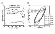
- 10(a) and 10(b) are diagrams showing measurement results of fatigue characteristics of MFS diode samples.
- 1 is a cross-sectional view of a semiconductor device according to an example
- FIG. 1 is a cross-sectional view of a semiconductor device according to an example
- HfN hafnium nitride
- Non-Patent Document 5 reports that HfN x has different crystal structures depending on the composition ratio x of Hf and N. Specifically, it is reported to have a rhombohedral crystal structure when HfN is 1.165 . However, there have been no reports that HfN exhibits ferroelectricity.
- the present inventor paid attention to the asymmetric structure of the rhombohedral system of HfNx , and got the idea that this asymmetric structure could realize an NfNx thin film having ferroelectricity.
- a semiconductor device includes a Si substrate and a ferroelectric thin film formed on the Si substrate and containing HfN x (1 ⁇ x) having a rhombohedral crystal structure.
- x when x is close to 1, it tends to have a metallic crystal structure, and when x approaches 1.33, it tends to have a crystal structure that is an insulating stable phase.
- the semiconductor device may further comprise a SiO2 layer formed on the Si substrate and outside the active area in which the semiconductor device is formed.
- the SiO 2 layer can suppress leakage from the sides of the device and improve device characteristics.
- a semiconductor device may comprise a contact layer comprising HfN y (y ⁇ 1) formed over a ferroelectric thin film, and a metal electrode formed over the contact layer.
- HfN y HfN y
- metal electrode formed over the contact layer.
- the ferroelectric thin film may have a thickness of 3 nm to 20 nm.
- a method for forming a ferroelectric thin film comprising depositing Hf on a Si substrate by ECR sputtering in a gas atmosphere containing N 2 and Ar to form a HfN x (1 ⁇ x) layer. and heat-treating after the forming to crystallize the HfN x layer into a rhombohedral system.
- a semiconductor device includes a transistor.
- a transistor includes a Si substrate, a ferroelectric thin film formed in a gate region on the Si substrate and containing HfN x (1 ⁇ x) having a rhombohedral crystal structure, and a drain adjacent to the gate region of the Si substrate. and an n + layer formed in the region and the source region.
- the semiconductor device may further comprise a SiO2 layer formed on the Si substrate and outside the active area including the gate, source and drain regions. This can suppress leakage from the sides of the device and improve performance.
- a state in which member A is connected to member B refers to a case in which member A and member B are physically directly connected, or a case in which member A and member B are electrically connected to each other. It also includes the case of being indirectly connected via other members that do not substantially affect the connected state or impair the functions and effects achieved by their combination.
- the state in which member C is provided between member A and member B refers to the case where member A and member C or member B and member C are directly connected, as well as the case where they are electrically connected. It also includes the case of being indirectly connected through other members that do not substantially affect the physical connection state or impair the functions and effects achieved by their combination.
- FIG. 1 is a cross-sectional view showing the basic structure of a semiconductor device 100 according to an embodiment.
- a semiconductor device 100A includes a Si substrate 110 and a ferroelectric thin film 120.
- the Si substrate 110 can be a p + -Si (100) substrate or a p-Si (100) substrate.
- a ferroelectric thin film 120 is formed on the Si substrate 110 and includes HfN x (1 ⁇ x).
- the composition ratio x is in the range of 1.1 ⁇ x ⁇ 1.3, preferably 1.15 ⁇ x ⁇ 1.2.
- the ferroelectric thin film 120 may have a thickness of 3 nm to 20 nm, for example 10 nm.
- FIG. 2 is a diagram showing the crystal structure of HfNx .
- HfN x has a cubic crystal structure, but as the composition ratio x increases, it has an inclined crystal structure, and eventually has a rhombohedral crystal structure.
- the crystal structure of the ferroelectric thin film 120 is determined not only by the composition ratio x, but also by the combination with the heat treatment conditions.
- the ferroelectric thin film 120 has a rhombohedral crystal structure, so the composition ratio x and the heat treatment conditions in the manufacturing process should be determined so as to have a rhombohedral asymmetric structure. Just do it.
- the above is the basic configuration of the semiconductor device 100 .
- the lamination structure of the ferroelectric thin films 110 and 120 is a ferroelectric-semiconductor lamination structure, and if a metal electrode is formed thereon, it becomes an MFS structure.
- various semiconductor devices such as diodes and transistors can be constructed based on the basic structure of FIG.
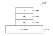
- FIG. 3 is a cross-sectional view of a semiconductor device 100A according to one embodiment.
- This semiconductor device 100A has an MFS structure and includes a Si substrate 110, a ferroelectric thin film 120, a contact layer 130 and a metal electrode 140.
- FIG. 1 is a cross-sectional view of a semiconductor device 100A according to one embodiment.
- This semiconductor device 100A has an MFS structure and includes a Si substrate 110, a ferroelectric thin film 120, a contact layer 130 and a metal electrode 140.
- a contact layer 130 comprising HfN y (y ⁇ 1) is formed over the ferroelectric thin film 120 .
- a metal electrode 140 is a metal such as Al and is formed on the contact layer 130 . Polycrystalline Si, TiN, W, Pt, etc. can be used for the metal electrode 140 in addition to Al.
- the ferroelectric thin film 120 may have a thickness of 3 nm to 20 nm, eg 10 nm, and the contact layer 130 may have a thickness of 10 nm to 30 nm, eg 20 nm.
- an electrode is added to the Si substrate 110 side of this MFS structure, it becomes an MFS diode. Also, by forming a drain and a source on the Si substrate 110, a transistor having a metal electrode 140 as a gate can be formed.
- FIG. 4 is a cross-sectional view of a semiconductor device 100B according to one embodiment.
- This semiconductor device 100B is an MFS diode, and has a back surface electrode 150 in addition to the MFS structure of FIG.
- the back electrode 150 can be made of a metal material such as Al.
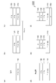
- 5A to 5F are diagrams for explaining the manufacturing method of the semiconductor device 100B of FIG.
- the Si substrate 110 is chemically cleaned.
- SPM sulfuric acid/hydrogen peroxide
- DHF dilute hydrofluoric acid
- a ferroelectric thin film 120 of HfN x (x>1) is formed on the Si substrate 110 .
- a contact layer 130 of HfN x (x ⁇ 1) is formed on the ferroelectric thin film 120 .
- the ferroelectric thin film 120 and contact layer 130 in FIGS. 5(b) and 5(c) can be formed in-situ by sputtering at room temperature.
- An ECR sputtering method can be used for the sputtering, and HfNx and HfNy can be formed by switching the atmosphere gas (the concentration of N 2 ).
- heat treatment is performed to crystallize the HfNx of the ferroelectric thin film 120 into a rhombohedral system.
- the heat treatment may be a PMA (Post-Metallization-Anneal) treatment or a PDA (Post-Deposition Anneal) treatment.
- a metal electrode 140 is formed on the contact layer 130 by thermal evaporation or the like, and if necessary, patterning is performed by dry etching. Then, as shown in FIG. 5( f ), a back surface electrode 150 is formed on the back surface of the Si substrate 110 . Like the metal electrode 140, Al is suitable for the material of the back electrode 150, but polycrystalline Si, TiN, W, Pt, etc. can also be used.
- the above is an example of the manufacturing method of the semiconductor device 100B.
- the lamination structure of the ferroelectric thin film 120 and the contact layer 130 can be formed by switching the atmosphere gas by the in-situ process. Therefore, it is advantageous in terms of manufacturing cost and manufacturing time.
- a sample of the semiconductor device 100B actually manufactured (referred to as a diode sample) and its evaluation will be described.
- each layer of the fabricated diode sample is as follows. Ferroelectric thin film 120 10 nm Contact layer 130 20 nm Also, the upper electrode 140 is 50 ⁇ 50 ⁇ m 2 .
- each layer The conditions for forming each layer are as follows.
- the substrate cleaning in FIG. 5(a) was performed by two cycles of SPM and DHF.
- the ferroelectric thin film 120 and the contact layer 130 shown in FIGS. 5(b) and 5(c) were deposited at room temperature by the ECR sputtering method.
- the heat treatment shown in FIG. 5(d) was performed with PMA or PDA for each sample. Both PMA and PDA are conducted at 400° C./5 minutes to 500° C./5 minutes in N 2 (1SLM) atmosphere for each sample.
- FIG. 6 is a diagram showing the relationship between the gas flow ratio during deposition of HfNx and the composition ratio of Hf and N.
- N 2 /(Ar+N 2 ) 50%, so the composition ratio x is 1. .15.
- the composition ratio y is 0.5. presumed to be. Since the relationship in FIG.
- composition ratios x and y estimated based on the gas flow rate ratio contain an error, and the error is considered to be about 20% at maximum. Therefore, the composition ratio x in the actual crystal is at least within the range of 0.9 ⁇ x ⁇ 1.4, and the composition ratio y is within the range of 0.4 ⁇ y ⁇ 0.6. ing.
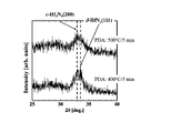
- FIG. 7 is a diagram showing the results of X-ray diffraction (XRD) measurement of the produced sample.
- FIG. 7 shows measurement results of a sample treated with PDA under conditions of 500° C./5 minutes and measurement results of a sample treated with PDA under conditions of 400° C./5 minutes. The measurement was performed after the heat treatment in FIG. 5(d) and before forming the electrodes.
- XRD X-ray diffraction
- FIG. 8 shows PV (polarization-voltage) characteristics of MFS diode samples.
- the horizontal axis indicates the applied voltage, and the vertical axis indicates polarization. From this result, it can be seen that the HfN x thin film having a rhombohedral crystal structure has ferroelectricity. This is a new finding that has not been known in the past.
- the coercive voltage 2V c that is, the voltage hysteresis width was 7.6 V
- the residual polarization amount 2P r was 24.0 ⁇ C/cm 2 .
- This value is significantly larger than the conventionally reported remanent polarization 2P r of HfO 2 to which no other element is added, which is 2.5 ⁇ C/cm 2 (Non-Patent Document 6).
- One of the reasons for this large amount of residual polarization is that the amount of displacement of nitrogen (N) atoms due to an electric field is larger than that of oxygen atoms.
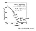
- FIG. 9 shows the CV (capacitance-voltage) characteristics of the MFS diode sample.
- the dielectric constant ⁇ r of HfNx exhibiting ferroelectricity described in this embodiment is estimated to be 23.
- Amorphous HfNx which is a high-dielectric-constant insulator, has a relative dielectric constant ⁇ r of about 14 to 18 (Non-Patent Document 4).
- 10(a) and 10(b) are diagrams showing measurement results of fatigue characteristics of MFS diode samples. From FIG. 10(a), it can be seen that when the number of cycles exceeds 10 10 , the characteristic deteriorates due to an increase in leakage, but it can be seen that it has a resistance to switching of 10 9 cycles, which is sufficient for practical use. value. Further, as shown in FIG. 10B, no imprint phenomenon is observed.
- FIG. 11 is a cross-sectional view of a semiconductor device 100C according to one embodiment.
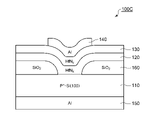
- This semiconductor device 100C is an MFS diode as in FIG. 4, and has a SiO 2 layer in addition to the MFS diode in FIG.
- this SiO 2 layer is formed outside the active region of the diode. Since the SiO 2 layer 160 is not inserted at the interface between the ferroelectric thin film 120 and the Si substrate 110 in the active region, the effect of the depolarizing electric field due to the SiO 2 layer 160 is not a problem.
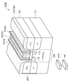
- FIG. 12 is a cross-sectional view of a semiconductor device 100D according to one example.
- This semiconductor device 100 ⁇ /b>D includes an MFS transistor 200 .
- Transistor 200 is formed on Si substrate 110 .
- the ferroelectric thin film 120 is a gate insulating film formed in the gate region on the Si substrate 110 and contains HfN x (1 ⁇ x) having a rhombohedral crystal structure.
- a SiO 2 layer 160 is formed on the Si substrate 110 to surround the active region 202 including the drain (D), gate (G) and source (S) of the transistor 200 .
- n + layers 112 and 114 are formed in the source region and drain region of the Si substrate 110 .
- a contact layer 130 is formed on the ferroelectric thin film 120. In FIG. 11, the ferroelectric thin film 120 and the contact layer 130 are shown integrally without showing the boundary between them.
- a metal electrode 140 serving as a gate electrode is formed on the ferroelectric thin film 120 (contact layer 130).
- a source electrode 170 and a drain electrode 172 are led out from the n + layers 112 and 114, respectively.
- the SiO 2 layer 160 may be omitted when forming the MFS transistor 200 as shown in FIG.
- the MFS device described above can be used as a cell of a non-volatile memory by utilizing changes in capacitance and threshold voltage.
- the application of the MFS device is not limited to non-volatile memory (digital storage element), but can be used as an analog storage element that utilizes continuous capacitance change and threshold change according to the gate voltage. Alternatively, it can be used as a D/A converter. Also, by using the floating gate device as a neural computing element in a neural network, it is expected to be applied to a neural device that mimics the human brain that performs weighting operations on input signals.
- the present invention relates to ferroelectric thin films.
Landscapes
- Chemical & Material Sciences (AREA)
- Inorganic Chemistry (AREA)
- General Chemical & Material Sciences (AREA)
- Chemical Kinetics & Catalysis (AREA)
- Engineering & Computer Science (AREA)
- Materials Engineering (AREA)
- Mechanical Engineering (AREA)
- Metallurgy (AREA)
- Organic Chemistry (AREA)
- Semiconductor Memories (AREA)
- Physics & Mathematics (AREA)
- Optics & Photonics (AREA)
- Crystallography & Structural Chemistry (AREA)
- Semiconductor Integrated Circuits (AREA)
Abstract
Description
本開示のいくつかの例示的な実施形態の概要を説明する。この概要は、後述する詳細な説明の前置きとして、実施形態の基本的な理解を目的として、1つまたは複数の実施形態のいくつかの概念を簡略化して説明するものであり、発明あるいは開示の広さを限定するものではない。またこの概要は、考えられるすべての実施形態の包括的な概要ではなく、実施形態の欠くべからざる構成要素を限定するものではない。便宜上、「一実施形態」は、本明細書に開示するひとつの実施形態(実施例や変形例)または複数の実施形態(実施例や変形例)を指すものとして用いる場合がある。
以下、本開示を、好適な実施の形態をもとに図面を参照しながら説明する。各図面に示される同一または同等の構成要素、部材、処理には、同一の符号を付するものとし、適宜重複した説明は省略する。また、実施の形態は、発明を限定するものではなく例示であって、実施の形態に記述されるすべての特徴やその組み合わせは、必ずしも発明の本質的なものであるとは限らない。
強誘電性薄膜120 10nm
コンタクト層130 20nm
また、上部電極140は、50×50μm2とした。
上述したMFSデバイスは、容量変化やしきい値電圧の変化を利用して、不揮発性メモリのセルとして利用することができる。
110 Si基板
120 強誘電性薄膜
130 コンタクト層
140 金属電極
150 裏面電極
160 SiO2層
200 トランジスタ
Claims (11)
- Si基板と、
前記Si基板上に形成され、菱面体晶系の結晶構造を有するHfNx(1<x)を含む強誘電性薄膜と、
を備えることを特徴とする半導体装置。 - 1.1≦x≦1.3であることを特徴とする請求項1に記載の半導体装置。
- 1.15≦x≦1.2であることを特徴とする請求項1または2に記載の半導体装置。
- 前記Si基板上であって、半導体デバイスが形成されるアクティブ領域の外側に形成されるSiO2層をさらに備えることを特徴とする請求項1から3のいずれかに記載の半導体装置。
- 前記強誘電性薄膜の上に形成される、HfNy(y<1)を含むコンタクト層と、
前記コンタクト層上に形成される金属電極と、
を備えることを特徴とする請求項1から4のいずれかに記載の半導体装置。 - 前記強誘電性薄膜の厚さは3nm~20nmであることを特徴とする請求項1から5のいずれかに記載の半導体装置。
- 強誘電性薄膜の形成方法であって、
Si基板上に、N2およびArを含むガス雰囲気中でHfをECR(Electron Cyclotron Resonance)スパッタ法により堆積し、HfNx(1<x)層を形成するステップと、
前記形成するステップの後に熱処理し、前記HfNx層を菱面体晶系に結晶化するステップと、
を備えることを特徴とする形成方法。 - トランジスタを備え、
前記トランジスタは、
Si基板と、
前記Si基板上のゲート領域に形成され、菱面体晶系の結晶構造を有するHfNx(1<x)を含む強誘電性薄膜と、
前記Si基板の前記ゲート領域と隣接するドレイン領域およびソース領域に形成されるn+層と、
を備えることを特徴とする半導体装置。 - 1.1≦x≦1.3であることを特徴とする請求項8に記載の半導体装置。
- 1.15≦x≦1.2であることを特徴とする請求項8または9に記載の半導体装置。
- 前記Si基板上であって、前記ゲート領域、前記ソース領域、前記ドレイン領域を含むアクティブ領域の外側に形成されるSiO2層をさらに備えることを特徴とする請求項8から10のいずれかに記載の半導体装置。
Priority Applications (3)
| Application Number | Priority Date | Filing Date | Title |
|---|---|---|---|
| JP2023505257A JP7759126B2 (ja) | 2021-03-11 | 2022-02-18 | 強誘電性薄膜の形成方法、それを備える半導体装置 |
| KR1020237028514A KR102960269B1 (ko) | 2021-03-11 | 2022-02-18 | 강유전성 박막의 형성 방법, 이를 구비하는 반도체 장치 |
| US18/281,445 US20240154035A1 (en) | 2021-03-11 | 2022-02-18 | Semiconductor apparatus and forming method for ferroelectric thin film |
Applications Claiming Priority (2)
| Application Number | Priority Date | Filing Date | Title |
|---|---|---|---|
| JP2021-039611 | 2021-03-11 | ||
| JP2021039611 | 2021-03-11 |
Publications (1)
| Publication Number | Publication Date |
|---|---|
| WO2022190817A1 true WO2022190817A1 (ja) | 2022-09-15 |
Family
ID=83227677
Family Applications (1)
| Application Number | Title | Priority Date | Filing Date |
|---|---|---|---|
| PCT/JP2022/006613 Ceased WO2022190817A1 (ja) | 2021-03-11 | 2022-02-18 | 強誘電性薄膜の形成方法、それを備える半導体装置 |
Country Status (3)
| Country | Link |
|---|---|
| US (1) | US20240154035A1 (ja) |
| JP (1) | JP7759126B2 (ja) |
| WO (1) | WO2022190817A1 (ja) |
Cited By (1)
| Publication number | Priority date | Publication date | Assignee | Title |
|---|---|---|---|---|
| US20240355895A1 (en) * | 2023-04-18 | 2024-10-24 | Zinite Corporation | Hafnium nitride adhesion layer |
Citations (3)
| Publication number | Priority date | Publication date | Assignee | Title |
|---|---|---|---|---|
| JP2005340721A (ja) * | 2004-05-31 | 2005-12-08 | Anelva Corp | 高誘電率誘電体膜を堆積する方法 |
| JP2021009893A (ja) * | 2019-06-28 | 2021-01-28 | 国立大学法人東京工業大学 | トランジスタおよび不揮発性メモリ、トランジスタの製造方法 |
| CN112349792A (zh) * | 2020-11-06 | 2021-02-09 | 浙江师范大学 | 一种单晶硅钝化接触结构及其制备方法 |
Family Cites Families (13)
| Publication number | Priority date | Publication date | Assignee | Title |
|---|---|---|---|---|
| US7768050B2 (en) * | 2006-07-07 | 2010-08-03 | The Trustees Of The University Of Pennsylvania | Ferroelectric thin films |
| JP2014103226A (ja) * | 2012-11-20 | 2014-06-05 | Mitsubishi Materials Corp | 強誘電体薄膜の製造方法 |
| EP3276689B1 (en) * | 2015-03-24 | 2021-05-05 | Sumitomo Chemical Company, Limited | Manufacturing method of niobate ferroelectric thin-film element |
| JP6566682B2 (ja) * | 2015-03-30 | 2019-08-28 | 住友化学株式会社 | 強誘電体薄膜素子の製造方法 |
| DE102017200678B4 (de) * | 2016-01-19 | 2019-06-27 | Fraunhofer-Gesellschaft zur Förderung der angewandten Forschung e.V. | Verfahren zur Herstellung einer Mikroelektronikschaltung sowie entsprechende Mikroelektronikschaltung |
| JP6751866B2 (ja) * | 2016-04-22 | 2020-09-09 | 国立研究開発法人産業技術総合研究所 | 半導体強誘電体記憶素子の製造方法及び半導体強誘電体記憶トランジスタ |
| US20170345831A1 (en) * | 2016-05-25 | 2017-11-30 | Micron Technology, Inc. | Ferroelectric Devices and Methods of Forming Ferroelectric Devices |
| TWI656625B (zh) * | 2017-11-14 | 2019-04-11 | 長庚大學 | Floating gate memory |
| US11532640B2 (en) * | 2020-05-29 | 2022-12-20 | Taiwan Semiconductor Manufacturing Co., Ltd. | Method for manufacturing a three-dimensional memory |
| US12051749B2 (en) * | 2020-06-23 | 2024-07-30 | Taiwan Semiconductor Manufacturing Company Limited | Interfacial dual passivation layer for a ferroelectric device and methods of forming the same |
| US11495618B2 (en) * | 2020-07-30 | 2022-11-08 | Taiwan Semiconductor Manufacturing Co., Ltd. | Three-dimensional memory device and method |
| US20220328651A1 (en) * | 2021-04-09 | 2022-10-13 | Cerfe Labs, Inc. | Semiconducting Ferroelectric Device with Silicon Doped Electrode |
| US20220352379A1 (en) * | 2021-04-29 | 2022-11-03 | Taiwan Semiconductor Manufacturing Company Limited | Ferroelectric memory devices having improved ferroelectric properties and methods of making the same |
-
2022
- 2022-02-18 WO PCT/JP2022/006613 patent/WO2022190817A1/ja not_active Ceased
- 2022-02-18 JP JP2023505257A patent/JP7759126B2/ja active Active
- 2022-02-18 US US18/281,445 patent/US20240154035A1/en active Pending
Patent Citations (3)
| Publication number | Priority date | Publication date | Assignee | Title |
|---|---|---|---|---|
| JP2005340721A (ja) * | 2004-05-31 | 2005-12-08 | Anelva Corp | 高誘電率誘電体膜を堆積する方法 |
| JP2021009893A (ja) * | 2019-06-28 | 2021-01-28 | 国立大学法人東京工業大学 | トランジスタおよび不揮発性メモリ、トランジスタの製造方法 |
| CN112349792A (zh) * | 2020-11-06 | 2021-02-09 | 浙江师范大学 | 一种单晶硅钝化接触结构及其制备方法 |
Non-Patent Citations (1)
| Title |
|---|
| OHMI, SHUN-ICHIRO ET AL. : "In-Situ N2-Plasma Nitridation for High-k HfN Gate Insulator Formed by Electron Cyclotoron Resonance Plasma Sputtering.", IEICE TRANSACTIONS ON ELECTRONICS, INSTITUTE OF ELECTRONICS, TOKYO, JP., vol. e103C, no. 6, 1 June 2020 (2020-06-01), Tokyo, JP. , pages 299 - 302, XP009539574, ISSN: 0916-8524 * |
Cited By (1)
| Publication number | Priority date | Publication date | Assignee | Title |
|---|---|---|---|---|
| US20240355895A1 (en) * | 2023-04-18 | 2024-10-24 | Zinite Corporation | Hafnium nitride adhesion layer |
Also Published As
| Publication number | Publication date |
|---|---|
| KR20230156031A (ko) | 2023-11-13 |
| JPWO2022190817A1 (ja) | 2022-09-15 |
| US20240154035A1 (en) | 2024-05-09 |
| JP7759126B2 (ja) | 2025-10-23 |
Similar Documents
| Publication | Publication Date | Title |
|---|---|---|
| JP7566397B2 (ja) | ロジックスイッチング素子及びその製造方法 | |
| KR20250036793A (ko) | 박막 구조체 및 이를 포함하는 반도체 소자 | |
| Lomenzo et al. | Ferroelectric Si-doped HfO 2 device properties on highly doped germanium | |
| US9853150B1 (en) | Method of fabricating epitaxial gate dielectrics and semiconductor device of the same | |
| CN107452742B (zh) | 半导体强电介质存储元件的制造方法和半导体强电介质存储晶体管 | |
| CN114975617A (zh) | 铁电场效晶体管装置 | |
| US20220367665A1 (en) | Method for forming semiconductor structure | |
| TW202236272A (zh) | 記憶體元件、形成其的方法及包括記憶單元的記憶體元件 | |
| KR102778194B1 (ko) | 로직 스위칭 소자 및 그 제조방법 | |
| Lee et al. | Hysteresis-free gate-all-around stacked poly-Si nanosheet channel ferroelectric Hf x Zr 1-x O 2 negative capacitance FETs with internal metal gate and NH 3 plasma nitridation | |
| Li et al. | Understanding the effect of oxygen content on ferroelectric properties of Al-doped HfO thin films | |
| Lo et al. | Fabrication of bilayer stacked antiferroelectric/ferroelectric Hf x Zr 1-x O 2 FeRAM and FeFET with improved leakage current and robust reliability by modifying atomic layer deposition temperatures | |
| Hsieh et al. | In Situ O₂ Plasma-Treated HfO₂–ZrO₂ Superlattice HZO FeRAMs Exhibiting Enhanced Remnant Polarization and Improved Endurance Performance | |
| JP7759126B2 (ja) | 強誘電性薄膜の形成方法、それを備える半導体装置 | |
| CN116344345A (zh) | 铁电场效应晶体管及其制备方法和铁电存储器 | |
| CN115275006A (zh) | 基于ZrO2插层的多比特铁电场效应晶体管及其制备方法 | |
| JP7357901B2 (ja) | トランジスタおよび不揮発性メモリ | |
| JP2010062221A (ja) | 強誘電体ゲート電界効果トランジスタ、それを用いたメモリ素子及び強誘電体ゲート電界効果トランジスタの製造方法 | |
| KR102960269B1 (ko) | 강유전성 박막의 형성 방법, 이를 구비하는 반도체 장치 | |
| Zhang et al. | Leakage Study of Ferroelectric AlScN Capacitors Prepared on Different Bottom Electrodes | |
| TWI866096B (zh) | 鐵電結構、積體電路與其形成方法 | |
| KR102861788B1 (ko) | 상부 게이트 구조의 강유전체 전계효과 트랜지스터, 이의 제조방법 및 이를 포함하는 메모리 소자 | |
| JP2008053554A (ja) | 電子デバイスとその製造方法 | |
| US20260135034A1 (en) | Capacitor and method for manufacturing same | |
| KR20040079884A (ko) | 갈륨나이트라이드를 기판으로한 페로브스카이트 구조의강유전체 박막트랜지스터 및 그 제조방법 |
Legal Events
| Date | Code | Title | Description |
|---|---|---|---|
| 121 | Ep: the epo has been informed by wipo that ep was designated in this application |
Ref document number: 22766780 Country of ref document: EP Kind code of ref document: A1 |
|
| WWE | Wipo information: entry into national phase |
Ref document number: 2023505257 Country of ref document: JP |
|
| WWE | Wipo information: entry into national phase |
Ref document number: 18281445 Country of ref document: US |
|
| NENP | Non-entry into the national phase |
Ref country code: DE |
|
| 122 | Ep: pct application non-entry in european phase |
Ref document number: 22766780 Country of ref document: EP Kind code of ref document: A1 |