WO2022190664A1 - 表示システム - Google Patents
表示システム Download PDFInfo
- Publication number
- WO2022190664A1 WO2022190664A1 PCT/JP2022/002069 JP2022002069W WO2022190664A1 WO 2022190664 A1 WO2022190664 A1 WO 2022190664A1 JP 2022002069 W JP2022002069 W JP 2022002069W WO 2022190664 A1 WO2022190664 A1 WO 2022190664A1
- Authority
- WO
- WIPO (PCT)
- Prior art keywords
- period
- mirror
- display device
- display
- temperature
- Prior art date
- Legal status (The legal status is an assumption and is not a legal conclusion. Google has not performed a legal analysis and makes no representation as to the accuracy of the status listed.)
- Ceased
Links
Images



Classifications
-
- G—PHYSICS
- G02—OPTICS
- G02B—OPTICAL ELEMENTS, SYSTEMS OR APPARATUS
- G02B27/00—Optical systems or apparatus not provided for by any of the groups G02B1/00 - G02B26/00, G02B30/00
- G02B27/01—Head-up displays
- G02B27/0101—Head-up displays characterised by optical features
-
- G—PHYSICS
- G02—OPTICS
- G02B—OPTICAL ELEMENTS, SYSTEMS OR APPARATUS
- G02B27/00—Optical systems or apparatus not provided for by any of the groups G02B1/00 - G02B26/00, G02B30/00
- G02B27/01—Head-up displays
-
- G—PHYSICS
- G02—OPTICS
- G02F—OPTICAL DEVICES OR ARRANGEMENTS FOR THE CONTROL OF LIGHT BY MODIFICATION OF THE OPTICAL PROPERTIES OF THE MEDIA OF THE ELEMENTS INVOLVED THEREIN; NON-LINEAR OPTICS; FREQUENCY-CHANGING OF LIGHT; OPTICAL LOGIC ELEMENTS; OPTICAL ANALOGUE/DIGITAL CONVERTERS
- G02F1/00—Devices or arrangements for the control of the intensity, colour, phase, polarisation or direction of light arriving from an independent light source, e.g. switching, gating or modulating; Non-linear optics
- G02F1/01—Devices or arrangements for the control of the intensity, colour, phase, polarisation or direction of light arriving from an independent light source, e.g. switching, gating or modulating; Non-linear optics for the control of the intensity, phase, polarisation or colour
- G02F1/13—Devices or arrangements for the control of the intensity, colour, phase, polarisation or direction of light arriving from an independent light source, e.g. switching, gating or modulating; Non-linear optics for the control of the intensity, phase, polarisation or colour based on liquid crystals, e.g. single liquid crystal display cells
- G02F1/133—Constructional arrangements; Operation of liquid crystal cells; Circuit arrangements
- G02F1/13306—Circuit arrangements or driving methods for the control of single liquid crystal cells
-
- G—PHYSICS
- G09—EDUCATION; CRYPTOGRAPHY; DISPLAY; ADVERTISING; SEALS
- G09G—ARRANGEMENTS OR CIRCUITS FOR CONTROL OF INDICATING DEVICES USING STATIC MEANS TO PRESENT VARIABLE INFORMATION
- G09G3/00—Control arrangements or circuits, of interest only in connection with visual indicators other than cathode-ray tubes
- G09G3/001—Control arrangements or circuits, of interest only in connection with visual indicators other than cathode-ray tubes using specific devices not provided for in groups G09G3/02 - G09G3/36, e.g. using an intermediate record carrier such as a film slide; Projection systems; Display of non-alphanumerical information, solely or in combination with alphanumerical information, e.g. digital display on projected diapositive as background
- G09G3/002—Control arrangements or circuits, of interest only in connection with visual indicators other than cathode-ray tubes using specific devices not provided for in groups G09G3/02 - G09G3/36, e.g. using an intermediate record carrier such as a film slide; Projection systems; Display of non-alphanumerical information, solely or in combination with alphanumerical information, e.g. digital display on projected diapositive as background to project the image of a two-dimensional display, such as an array of light emitting or modulating elements or a CRT
-
- G—PHYSICS
- G09—EDUCATION; CRYPTOGRAPHY; DISPLAY; ADVERTISING; SEALS
- G09G—ARRANGEMENTS OR CIRCUITS FOR CONTROL OF INDICATING DEVICES USING STATIC MEANS TO PRESENT VARIABLE INFORMATION
- G09G2310/00—Command of the display device
- G09G2310/08—Details of timing specific for flat panels, other than clock recovery
-
- G—PHYSICS
- G09—EDUCATION; CRYPTOGRAPHY; DISPLAY; ADVERTISING; SEALS
- G09G—ARRANGEMENTS OR CIRCUITS FOR CONTROL OF INDICATING DEVICES USING STATIC MEANS TO PRESENT VARIABLE INFORMATION
- G09G2320/00—Control of display operating conditions
- G09G2320/04—Maintaining the quality of display appearance
- G09G2320/041—Temperature compensation
-
- G—PHYSICS
- G09—EDUCATION; CRYPTOGRAPHY; DISPLAY; ADVERTISING; SEALS
- G09G—ARRANGEMENTS OR CIRCUITS FOR CONTROL OF INDICATING DEVICES USING STATIC MEANS TO PRESENT VARIABLE INFORMATION
- G09G2330/00—Aspects of power supply; Aspects of display protection and defect management
- G09G2330/04—Display protection
- G09G2330/045—Protection against panel overheating
-
- G—PHYSICS
- G09—EDUCATION; CRYPTOGRAPHY; DISPLAY; ADVERTISING; SEALS
- G09G—ARRANGEMENTS OR CIRCUITS FOR CONTROL OF INDICATING DEVICES USING STATIC MEANS TO PRESENT VARIABLE INFORMATION
- G09G2380/00—Specific applications
- G09G2380/10—Automotive applications
-
- G—PHYSICS
- G09—EDUCATION; CRYPTOGRAPHY; DISPLAY; ADVERTISING; SEALS
- G09G—ARRANGEMENTS OR CIRCUITS FOR CONTROL OF INDICATING DEVICES USING STATIC MEANS TO PRESENT VARIABLE INFORMATION
- G09G3/00—Control arrangements or circuits, of interest only in connection with visual indicators other than cathode-ray tubes
- G09G3/20—Control arrangements or circuits, of interest only in connection with visual indicators other than cathode-ray tubes for presentation of an assembly of a number of characters, e.g. a page, by composing the assembly by combination of individual elements arranged in a matrix no fixed position being assigned to or needed to be assigned to the individual characters or partial characters
- G09G3/34—Control arrangements or circuits, of interest only in connection with visual indicators other than cathode-ray tubes for presentation of an assembly of a number of characters, e.g. a page, by composing the assembly by combination of individual elements arranged in a matrix no fixed position being assigned to or needed to be assigned to the individual characters or partial characters by control of light from an independent source
- G09G3/36—Control arrangements or circuits, of interest only in connection with visual indicators other than cathode-ray tubes for presentation of an assembly of a number of characters, e.g. a page, by composing the assembly by combination of individual elements arranged in a matrix no fixed position being assigned to or needed to be assigned to the individual characters or partial characters by control of light from an independent source using liquid crystals
Definitions
- the present invention relates to display systems.
- HUD Head Up Display
- Patent Document 1 A so-called head-up display (HUD: Head Up Display) that projects an image onto a translucent member such as glass is known (for example, Patent Document 1).
- sunlight may enter the display device through the optical system.
- the temperature of the place where the light hits becomes high, which may adversely affect the display device. Therefore, it is necessary to limit the incidence of sunlight, which causes temperature rise.
- the present invention has been made in view of the above problems, and an object of the present invention is to provide a display system capable of limiting the incidence of sunlight and suppressing the temperature rise of the display device.
- a display system includes a display device and a mirror device that reflects an image of the display device and projects it onto a projection plate, and the mirror device has a plurality of areas that reflect the image.
- a temperature sensor section that is divided into partial areas and detects the temperature of a plurality of the partial areas; a liquid crystal mirror section that is arranged opposite to the temperature sensor section and is capable of switching between a reflection state and a transmission state of incident light; and a control circuit for controlling a light reflection state and a light transmission state of the partial area according to the temperature detected in the partial area.
- FIG. 1 is an explanatory diagram schematically explaining a display system according to an embodiment.
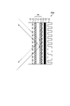
- FIG. 2A is a cross-sectional view showing the configuration of the mirror device.
- FIG. 2B is a cross-sectional view showing the configuration of the mirror device.
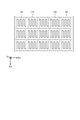
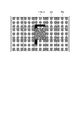
- FIG. 3 is a plan view of the temperature sensor section.
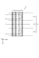
- FIG. 4 is a diagram showing an example of a cross-sectional structure of a liquid crystal mirror section.
- FIG. 5 is a plan view showing the arrangement of the second electrodes of the liquid crystal mirror section.
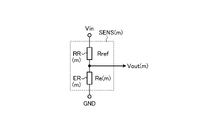
- FIG. 6 is a configuration diagram of a temperature sensor.
- FIG. 7 is a diagram for explaining a specific operation example of the mirror device.
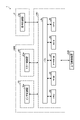
- FIG. 8 is a diagram illustrating an example of a control system of the display system according to the embodiment;
- FIG. 8 is a diagram illustrating an example of a control system of the display system according to the embodiment;
- FIG. 8 is a diagram illustrating an example of a control system of the display system according to the embodiment; FIG.
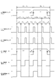
- FIG. 9 is a timing chart showing an example of control timing of the temperature sensor section and the liquid crystal mirror section of the mirror device.
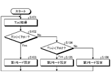
- FIG. 10 is a flowchart showing an example of mirror control mode setting processing.
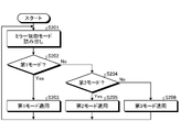
- FIG. 11 is a flowchart illustrating an example of mirror control mode application processing.
- FIG. 1 is an explanatory diagram schematically explaining the display system according to the embodiment.
- the display system 1 according to the embodiment is, for example, a head-up display (HUD: Head Up Display, hereinafter simply referred to as "HUD 1") as shown in FIG.
- the HUD 1 includes a display device 2, an optical system RM that reflects an image of the display device 2 and projects it onto the projection plate WS, and a housing 4 that houses the display device 2 and the optical system RM.
- the display device 2 is, for example, a liquid crystal display device in which light emitted from a light source unit is transmitted through a liquid crystal display panel and projected as an image.
- the display device 2 is not limited to a liquid crystal display device.
- it is equipped with a self-luminous display panel such as an organic EL using an OLED (Organic Light Emitting Diode) or a ⁇ LED (micro LED) as a display element. It may be in a different form.
- the image light L emitted from the display device 2 is reflected by the optical system RM including the mirror device RM1 and the mirror member RM2, guided to the projection plate WS, and reflected by the projection plate WS to reach the user H. , it is recognized as an image VI within the user H's field of view.
- the projection plate WS may be any translucent member positioned on the user's H line of sight.
- the projection plate WS is, for example, a windshield of a vehicle, a windshield, or a translucent plate member called a combiner provided separately from the windshield.
- the sunlight LL may enter the opening 4S of the housing 4 on the HUD 1 .
- the sunlight LL may be guided to the optical system RM and condensed toward the display device 2 . Since the concentrated sunlight may cause an abnormality in the display device 2 during operation, the incidence of the sunlight LL on the display device 2 is restricted to partially increase the temperature of the display area. is desired to be suppressed.
- the mirror device RM1 includes a temperature sensor section 10 and a liquid crystal mirror section 20. As shown in FIG. As shown in FIG. 2A, the temperature sensor section 10 and the liquid crystal mirror section 20 are located on the incident surface side of the image light L or the sunlight LL emitted from the display device 2 (hereinafter also simply referred to as "incident surface side").
- the temperature sensor unit 10 may be provided on the back side of the temperature sensor unit 10, and the liquid crystal mirror unit 20 may be provided on the back side of the temperature sensor unit 10 with the first transparent insulating layer 31 interposed therebetween.
- the liquid crystal mirror section 20 may be provided on the incident surface side, and the temperature sensor section 10 may be provided on the rear side of the liquid crystal mirror section 20 with the first transparent insulating layer 31 interposed therebetween.
- the absorption layer 40 is provided on the back side of the liquid crystal mirror section 20 with the second transparent insulating layer 32 interposed therebetween, and the heat dissipation layer 50 is provided on the back side of the absorption layer 40.
- an absorption layer 40 is provided on the back side of the temperature sensor section 10 with the second transparent insulating layer 32 interposed therebetween, and a heat radiation layer 50 is provided via the absorption layer 40 .
- the absorption layer 40 is exemplified by, for example, a black-colored organic material or inorganic material.
- the heat dissipation layer 50 is exemplified by, for example, a heat sink and a heat dissipation sheet.
- the liquid crystal mirror section 20 is provided with a first polarizing plate 21 and a second polarizing plate 22 with a liquid crystal layer LC interposed therebetween.
- Image light L emitted from the display device 2 passes through the first polarizing plate 21 and the liquid crystal layer LC, is reflected by the second polarizing plate 22 , and passes through the liquid crystal layer LC and the first polarizing plate 21 .
- the sunlight LL passes through the first polarizing plate 21 and the liquid crystal layer LC, is reflected by the second polarizing plate 22 , and passes through the liquid crystal layer LC and the first polarizing plate 21 .
- the temperature sensor section 10 may be separated from the liquid crystal mirror section 20 , or may be in contact with or adhered to the liquid crystal mirror section 20 . Also, the temperature sensor section 10 may be provided integrally with the liquid crystal mirror section 20 .
- FIG. 3 is a plan view of the temperature sensor section.
- FIG. 4 is a diagram showing an example of a cross-sectional structure of a liquid crystal mirror section.
- FIG. 5 is a plan view showing the arrangement of the second electrodes of the liquid crystal mirror section.
- an area SA that reflects the image light L emitted from the display device 2 is divided into a plurality of partial areas PA.
- An area SA in the mirror device RM1 is an area corresponding to the display area of the display device 2 .
- Temperature sensor unit 10 detects the temperature of a plurality of partial areas PA.
- a plurality of partial areas PA on the temperature sensor section 10 are areas in which a plurality of temperature detection resistance elements ER are provided.
- FIG. 3 exemplifies a total of 15 partial areas PA in which five partial areas PA are arranged in the first direction Dx and three partial areas PA are arranged in the second direction Dy. Not limited. For example, it is possible to employ a configuration in which four partial areas PA are arranged in the first direction Dx and three partial areas PA are arranged in the second direction Dy to form a total of 12 partial areas PA.
- first direction Dx is one direction in a plane parallel to the substrate of the temperature sensor section 10 .
- the second direction Dy is one direction in a plane parallel to the base material of the temperature sensor section 10 and is a direction orthogonal to the first direction Dx. Note that the second direction Dy may not be perpendicular to the first direction Dx, but may intersect with it.
- a third direction Dz is a direction orthogonal to the first direction Dx and the second direction Dy, and is a normal direction of the substrate of the temperature sensor section 10 .
- the temperature detection resistance element ER is an electric resistance made of an alloy, a compound containing a metal (metallic compound), or a metal.
- the resistance element ER may be a laminate in which a plurality of types of materials corresponding to at least one of metals, alloys, and metal compounds are laminated. When describing an alloy or the like in the description of the embodiments, it means a material that can be employed as the composition of the resistance element ER.
- the temperature detection resistor element ER has a configuration in which a plurality of L-shaped wirings having long sides along the second direction Dy are connected in the first direction Dx. In this aspect, a plurality of L-shaped wirings are connected such that short sides of two L-shaped wirings adjacent to each other in the first direction Dx alternate in the second direction Dy to form the temperature detection resistor element. Forms of ER are formed.
- the temperature sensor section 10 is provided with, for example, a plurality of reference resistance elements RR which are connected in series with a plurality of temperature detection resistance elements ER and respectively constitute a temperature sensor (see FIG. 6).
- a plurality of reference resistance elements RR are provided, for example, in an area outside the area SA. The present disclosure is not limited by the manner of arrangement of the plurality of reference resistance elements RR.
- FIG. 6 is a configuration diagram of the temperature sensor.
- the temperature sensor SENS(m) has a reference resistance element RR(m) and a temperature detection resistance element ER(m) electrically connected in series between an input potential Vin and a reference potential GND. Connected and configured.
- the temperature sensor SENS(m) outputs an output potential Vout(m) corresponding to the volume resistivity of the temperature detection resistance element ER(m).
- the potential at the connection point between the temperature detection resistance element ER(m) and the reference resistance element RR(m) is output as the output potential Vout(m) of the temperature sensor SENS(m).
- the current generated according to the input potential Vin tries to flow to the reference potential GND, but the current reaches the reference potential GND according to the volume resistivity of the temperature detection resistance element ER(m).
- a current is generated by blocking the flow to This current produces the output potential Vout(m). That is, the higher the volume resistivity of the temperature detection resistor element ER(m), the higher the output potential Vout(m).
- the output potential Vout(m) of the temperature sensor SENS(m) is given by the following ( 1) Represented by the formula.
- Vout(m) [Re(m)/ ⁇ Re(m)+Rref ⁇ ] ⁇ Vin...(1)
- the first coefficient a(m) and the second coefficient b(m) are eigenvalues for compensating for variations in electrical characteristics of the temperature detection resistive element ER(m). It becomes a different value for each resistance element ER(m). Therefore, when calculating the temperature of each partial area PA detected by the temperature sensor SENS(m), each different first coefficient a( m) and each second coefficient b(m). Thereby, the accuracy of the temperature calculation result can be improved.
- the liquid crystal mirror section 20 includes a first substrate 23, a second substrate 24, a first electrode 25, and a second electrode 26.
- the first electrode 25 and the second electrode 26 are provided facing each other in the third direction Dz with the liquid crystal layer LC interposed therebetween.
- the first electrode 25 is provided on the first base material 23 .
- a second electrode 26 is provided on the second substrate 24 .
- the liquid crystal mirror section 20 is arranged to face the temperature sensor section 10 in the third direction Dz. As shown in FIG. 5 , the plurality of partial areas PA on the liquid crystal mirror section 20 are areas in which the plurality of second electrodes 26 are provided on the second substrate 24 . The liquid crystal mirror section 20 reflects or transmits light incident on the liquid crystal mirror section 20 by controlling the potential difference between the first electrode 25 and the second electrode 26 .
- the partial regions PA1 and PA3 provided with the second electrode 26 are The incident light is reflected by the liquid crystal mirror section 20 .
- the liquid crystal mirror section 20 may reflect or transmit the light incident on the liquid crystal mirror section 20 by controlling the potential difference between the first electrode 25 and the second electrode 26, and the above-described mode may be used. is not limited to For example, when a predetermined potential difference is applied between the first electrode 25 and the second electrode 26, light incident on the partial areas PA1 and PA3 provided with the second electrode 26 is reflected by the liquid crystal mirror section 20. However, when no potential difference is applied between the first electrode 25 and the second electrode 26, light incident on the partial area PA2 provided with the second electrode 26 is transmitted through the liquid crystal mirror section 20. can be The present disclosure is not limited by the control mode of the liquid crystal mirror section 20 .
- FIG 4 and 5 show examples in which one second electrode 26 is provided corresponding to one partial area PA, a plurality of second electrodes 26 are provided corresponding to one partial area PA.
- the provided aspect may be sufficient.
- FIG. 7 is a diagram explaining a specific operation example of the mirror device.
- FIG. 7 shows a specific example of an image projected onto the projection plate WS.
- the partial area PA(m) is in the transmissive state, and the areas other than the partial area PA(m) are in the reflective state.
- the image projected onto the projection plate WS is projected onto the projection plate WS with the image missing in the area corresponding to the partial area PA(m) of the temperature sensor section 10 .
- the time ratio of reflection and transmission of the partial area PA whose temperature is detected by the temperature sensor SENS of the temperature sensor unit 10 is changed according to the temperature detected by the temperature sensor SENS.
- a reflective period and a transmissive period are provided in one frame period of the display device 2, and the ratio between the reflective period and the transmissive period of each partial area PA is changed according to the temperature detected in each partial area PA. do. More specifically, in an area (first area) where the temperature detected in each partial area PA is equal to or higher than a predetermined threshold, an area (first area) where the temperature detected in each partial area PA is less than a predetermined threshold
- the transmission period in one frame period of the display device 2 is made longer than in the second area).
- FIG. 8 is a diagram showing an example of the control system of the display system according to the embodiment.
- the control circuit 100 is composed of, for example, a control IC packaged as a so-called one-chip IC (Integrated Circuit).
- the control circuit 100 may be configured by a plurality of ICs.
- the control circuit 100 communicates with the sensor control section 10 a that controls the temperature sensor section 10 and the mirror control section 20 a that controls the liquid crystal mirror section 20 .
- the control circuit 100 also communicates with an external host control device 200 .
- the present disclosure is not limited by the protocols, interfaces, etc. of communication between the control circuit 100 and the sensor control section 10a, the mirror control section 20a, and the host control device 200.
- the control circuit 100 may include, for example, some or all of the functions of the sensor control section 10a and the mirror control section 20a.
- the control circuit 100 includes a CPU (Central Processing Unit) 84, a bus 85, a ROM (Read Only Memory) 86, an EEPROM (Electrically Erasable Programmable Read Only Memory) 87, a RAM (Random Access Memory) 88, and a GPIO ( General Purpose Input Output) 89.
- CPU Central Processing Unit
- ROM Read Only Memory
- EEPROM Electrically Erasable Programmable Read Only Memory
- RAM Random Access Memory
- GPIO General Purpose Input Output
- the CPU 84 performs arithmetic processing necessary for controlling the mirror device RM1.
- the bus 85 functions as a transmission path for various digital signals within the control circuit 100 .
- CPU 84 , bus 85 , ROM 86 , EEPROM 87 , RAM 88 and GPIO 89 are connected to bus 85 .
- the ROM 86 unrewritably stores programs and the like.
- a program or the like refers to a software program that is read during processing performed by the CPU 84 and data that is referred to as the software program is executed.
- the EEPROM 87 rewritably stores programs and the like.
- the RAM 88 temporarily stores various data and parameters generated by the CPU 84 executing programs and the like.
- the GPIO 89 transmits signals to the outside in response to outputs from the CPU 84 and the like via the bus 85 .
- the GPIO 89 also functions as an input path for inputting an input such as a synchronization signal to the bus 85 from the display control unit 2 a that controls the display of the display device 2 .
- control circuit 100 controls the temperature sensor section 10 and the liquid crystal mirror section 20 of the mirror device RM1 in synchronization with the display frame rate of the display device 2 based on the synchronization signal input from the display control section 2a. conduct.
- FIG. 9 is a timing chart showing an example of control timing of the temperature sensor section and the liquid crystal mirror section of the mirror device.
- the "H" period of the display control timing indicates the display period DP
- the "L” period indicates the blanking period BL.
- the control circuit 100 acquires the temperature in each partial area PA(m) at, for example, twice the display frame rate (eg, 30 fps) of the display device 2 (eg, 60 fps). Specifically, the control circuit 100 acquires the temperature in each partial area PA(m) in synchronization with the rising from "L" to "H” of the sensor control timing shown in FIG.
- the control circuit 100 compares the temperature T(m) of each partial area PA(m) acquired at the sensor control timing shown in FIG. 9 with a preset temperature threshold.
- the temperature threshold is stored in the ROM 86 or EEPROM 87 of the control circuit 100, for example.
- temperature thresholds include a first threshold Tth1 (eg, 60° C.) and a second threshold Tth2 (eg, 80° C.) higher than the first threshold Tth1.
- the temperature sensor unit 10 is provided in the mirror device RM1.
- the control circuit 100 performs mirror control settings for each partial area PA(m) based on the comparison result of the temperature T(m) of each partial area PA(m) with the temperature threshold.
- the mirror control setting for each partial area PA(m) set by the control circuit 100 is also referred to as "mirror control mode".
- the "H" period of mirror control modes 1, 2, and 3 indicates a reflection period in which each partial area PA(m) is in a reflective state
- the "L" period indicates each partial area PA(m). It shows the transmission period for the transmission state.
- the control circuit 100 switches the mirror control mode to the area (first area) where the temperature T(m) of each partial area PA(m) is less than the first threshold value Tth1 (T(m) ⁇ Tth1).
- the display device 2 operates so as to repeat the reflective state and the transmissive state at the display frame rate (for example, 30 fps). Specifically, as shown in FIG. 9, the display device 2 is set to be in a reflective state during the display period DP and to be in a transmissive state during the blanking period BL.
- the control circuit 100 determines that the temperature T(m) of each partial area PA(m) is equal to or higher than the first threshold value Tth1 (T(m) ⁇ Tth1) and is lower than the second threshold value Tth2 (T(m) ⁇ Tth2 ) (the second area), the mirror control mode is set to the second mode.
- the reflective state and the transmissive state are repeated at twice (eg, 60 fps) the display frame rate (eg, 30 fps) of the display device 2 .
- the reflective state and the transmissive state are set to be repeated every quarter frame.
- control circuit 100 sets the mirror control mode to the third mode in a region (third region) where the temperature T(m) of each partial region PA(m) is equal to or higher than the second threshold value Tth2.
- the reflective state and the transmissive state are repeated at the display frame rate (eg, 30 fps) of the display device 2, and the transmissive period is longer than in the first mode.
- the transmissive period is longer than in the first mode.
- it is set to be in a reflective state in the first 1/4 frame period of one frame period, and to be in a transmissive state in the remaining 3/4 frame period.
- the transmission period (3/4 frame period) in one frame period of the area set to the third mode (third area) is equal to that of the area set to the second mode (second area) in one frame period. It is longer than the total period of the transmission period (1/2 frame period).
- control circuit 100 applies the mirror control mode to each partial area PA(m) at twice (eg, 60 fps) the display frame rate (eg, 30 fps) of the display device 2, for example. Specifically, the control circuit 100 applies the mirror control mode of each partial area PA(m) in synchronization with the rising from "L" to "H” of the mirror control timing shown in FIG.
- the partial area PA(m) is in the transmission state during the blanking period BL of the display device 2.
- the incidence of LL is restricted, and the temperature rise of the display device 2 can be suppressed.
- the transmission period in which the transmission state is maintained in one frame period is longer than in the first mode, so the amount of sunlight LL is greater than in the case of operation in the first mode. is limited, and the temperature rise of the display device 2 can be suppressed.
- the transmission period during which the transmission state is maintained in one frame period is longer than in the second mode, so the amount of sunlight is greater than in the case of operation in the second mode.
- the incidence of LL is restricted, and the temperature rise of the display device 2 can be suppressed.
- FIG. 10 is a flowchart showing an example of mirror control mode setting processing.
- FIG. 11 is a flowchart illustrating an example of mirror control mode application processing.
- the control circuit 100 acquires the temperature T(m) in each partial area PA(m) at the sensor control timing shown in FIG. 9 (step S101).
- the control circuit 100 performs a comparison process between the temperature T(m) of the partial area PA(m) acquired in step S101 and a preset threshold value.
- the control circuit 100 determines whether the temperature T(m) of the partial area PA(m) is less than a first threshold value Tth1 (eg, 60° C.) (T(m) ⁇ Tth1). (step S102).
- a first threshold value Tth1 eg, 60° C.
- control circuit 100 If temperature T(m) of partial area PA(m) is less than first threshold value Tth1 (T(m) ⁇ Tth1) (step S102; Yes), control circuit 100 performs mirror control on partial area PA(m). The mode is set to the first mode (step S103). At this time, the control circuit 100 temporarily stores, for example, the RAM 88 of the control circuit 100, a set value that is set to operate the partial area PA(m) in the first mode.
- step S102 If the temperature T(m) of the partial area PA(m) is equal to or higher than the first threshold value Tth1 (T(m) ⁇ Tth1) (step S102; No), then the control circuit 100 controls the partial area PA(m) is less than a second threshold value Tth2 (for example, 80° C.) (T(m) ⁇ Tth2) (step S104).
- Tth1 T(m) ⁇ Tth1
- Tth2 for example, 80° C.
- step S104 If the temperature T(m) of the partial area PA(m) is less than the second threshold value Tth2 (T(m) ⁇ Tth2) (step S104; Yes), the control circuit 100 performs mirror control on the partial area PA(m).
- the mode is set to the second mode (step S105).
- the control circuit 100 temporarily stores, for example, the RAM 88 of the control circuit 100, a set value that is set to operate the partial area PA(m) in the second mode.
- step S104 If the temperature T(m) of the partial area PA(m) is equal to or higher than the second threshold value Tth2 (T(m) ⁇ Tth2) (step S104; No), the control circuit 100 performs mirror control on the partial area PA(m).
- the mode is set to the third mode (step S106).
- the control circuit 100 temporarily stores, for example, the RAM 88 of the control circuit 100, a set value that is set to operate the partial area PA(m) in the third mode.
- mirror control mode setting process shown in FIG. 10 may be performed in parallel for each partial area PA(m), or may be performed in sequence for each partial area PA(m). can be
- the control circuit 100 reads the mirror control mode for each partial area PA(m) temporarily stored in the RAM 88 in the mirror control mode setting process shown in FIG. 10 (step S201).
- the control circuit 100 determines whether the mirror control mode for each partial area PA(m) is the first mode (step S202).
- step S202 If the mirror control mode for each partial area PA(m) is the first mode (step S202; Yes), the control circuit 100 applies the first mode as the mirror control mode for the partial area PA(m) (step S203). ).
- step S202 If the mirror control mode for each partial area PA(m) is not the first mode (step S202; No), then the control circuit 100 determines whether the mirror control mode for each partial area PA(m) is the second mode. It is determined whether or not (step S204).
- step S204 If the mirror control mode for each partial area PA(m) is the second mode (step S204; Yes), the control circuit 100 applies the second mode as the mirror control mode for the partial area PA(m) (step S205). ).
- step S204 If the mirror control mode for each partial area PA(m) is not the second mode (step S204; No), the control circuit 100 applies the third mode as the mirror control mode for the partial area PA(m) (step S206). .
- mirror control mode application process shown in FIG. 11 may be performed in parallel on each partial area PA(m), or may be performed in sequence on each partial area PA(m).
- mirror control mode setting process (FIG. 10) and mirror control mode application process (FIG. 11) are performed at the sensor control timing shown in FIG. Repeatedly executing at a frequency doubled (for example, 60 fps) limits the incidence of the sunlight LL on the display device 2 and suppresses the temperature rise of the display device 2 .
- a frequency doubled for example, 60 fps
- each partial area PA(m) was acquired at twice (eg, 60 fps) the display frame rate (eg, 30 fps) of the display device 2, but the sensor control timing is It is not limited to this.
- the temperature of the control circuit 100, the sensor control section 10a, and the mirror control section 20a may rise due to the incidence of the sunlight LL. Therefore, for example, when there is a partial area PA(m) whose temperature T(m) is equal to or higher than the second threshold value Tth2, each partial area PA(m) is displayed at the display frame rate of the display device 2 (for example, 30 fps). It is good also as an aspect which acquires the temperature in.
- the power consumption of the control circuit 100, the sensor control section 10a, and the mirror control section 20a can be reduced, so that the self-heating of the control circuit 100, the sensor control section 10a, and the mirror control section 20a is suppressed, and the temperature rise is suppressed. can be suppressed.
- the display system 1 employs the mirror device RM1 including the temperature sensor unit 10 and the liquid crystal mirror unit 20 in the optical system RM, and the In areas where the temperature is equal to or higher than a predetermined threshold, the transmission period in one frame period of the display device 2 is made longer than in areas where the temperature detected in each partial area PA is less than the predetermined threshold. As a result, the incidence of sunlight LL on the display device 2 is restricted, and a partial temperature rise in the display area of the display device 2 can be suppressed.
- the sunlight LL transmitted through the liquid crystal mirror section 20 is absorbed by the absorption layer 40 provided on the back side of the mirror device RM1 and radiated by the heat radiation layer 50 . Thereby, the temperature rise of the liquid crystal mirror section 20 can be suppressed.
- the mirror device RM1 including the temperature sensor section 10 and the liquid crystal mirror section 20 into the optical system RM of the existing display system (HUD), It is possible to cope with the temperature rise of the display panel without incorporating a sensor for detecting temperature.
- HUD 2 display device 4 housing 4S opening (housing) 10 temperature sensor section 10a sensor control section 20 liquid crystal mirror section 20a mirror control section 21 first polarizing plate 22 second polarizing plate 23 first base material 24 second base material 25 first electrode 26 second electrode 31 first transparent insulating layer 32 second transparent insulating layer 40 absorption layer 50 heat dissipation layer 84
- CPU 85 bus 86 ROM 87 EEPROM 88 RAM 89 GPIOs 100 control circuit 200 host controller a(m) first coefficient b(m) second coefficient ER(m) temperature detection resistance element GND reference potential LC liquid crystal layers PA, PA(m) partial region RM1 mirror device RM2 mirror member RR (m) Reference resistance element SENS (m) Temperature sensor T (m) Temperature Tth1 First threshold Tth2 Second threshold VI Image Vin Input potential Vout (m) Output potential WS Projection plate
Landscapes
- Physics & Mathematics (AREA)
- General Physics & Mathematics (AREA)
- Optics & Photonics (AREA)
- Engineering & Computer Science (AREA)
- Nonlinear Science (AREA)
- Computer Hardware Design (AREA)
- Theoretical Computer Science (AREA)
- Mathematical Physics (AREA)
- Chemical & Material Sciences (AREA)
- Crystallography & Structural Chemistry (AREA)
- Liquid Crystal (AREA)
Abstract
表示システム1は、表示装置2と、表示装置2の画像を反射して投影板へ投影するミラー装置RM1と、を備える。ミラー装置RM1は、画像を反射する領域が複数の部分領域に分割され、複数の部分領域の温度を検出する温度センサ部10と、温度センサ部10と対向配置され、入射された光の反射状態と透過状態とが切替可能な液晶ミラー部20と、部分領域において検出された温度に応じて、当該部分領域の光の反射状態と透過状態とを制御する制御回路100と、を備える。
Description
本発明は、表示システムに関する。
ガラス等の透光性を有する部材に対して画像を投影する所謂ヘッドアップディスプレイ(HUD:Head Up Display)が知られている(例えば、特許文献1)。
特許文献1の技術によると、太陽の光が光学系を介して表示装置に入射することがある。光学系により集光された太陽の光が表示装置に当たると、光が当たった場所が高温になって表示装置に悪影響を与えることがある。従って、温度上昇の要因となる太陽光の入射を制限する必要がある。
本発明は、上記の課題に鑑みてなされたもので、太陽光の入射を制限し、表示装置の温度上昇を抑制することができる表示システムを提供することを目的とする。
本発明の一態様に係る表示システムは、表示装置と、前記表示装置の画像を反射して投影板へ投影するミラー装置と、を備え、前記ミラー装置は、前記画像を反射する領域が複数の部分領域に分割され、複数の前記部分領域の温度を検出する温度センサ部と、前記温度センサ部と対向配置され、入射された光の反射状態と透過状態とが切替可能な液晶ミラー部と、前記部分領域において検出された温度に応じて、当該部分領域の光の反射状態と透過状態とを制御する制御回路と、を備える。
本発明を実施するための形態(実施形態)につき、図面を参照しつつ詳細に説明する。なお、以下の実施形態に記載した内容により本発明が限定されるものではない。また、以下に記載した構成要素には、当業者が容易に想定できるもの、実質的に同一のものが含まれる。さらに、以下に記載した構成要素は適宜組み合わせることが可能である。また、開示はあくまで一例にすぎず、当業者において、発明の主旨を保っての適宜変更について容易に想到し得るものについては、当然に本発明の範囲に含有されるものである。また、図面は説明をより明確にするため、実際の態様に比べ、各部の幅、厚さ、形状等について模式的に表される場合があるが、あくまで一例であって、本発明の解釈を限定するものではない。また、本明細書と各図において、既出の図に関して前述したものと同様の要素には、同一の符号を付して、詳細な説明を適宜省略することがある。
図1は、実施形態に係る表示システムを模式的に説明する説明図である。実施形態に係る表示システム1は、例えば図1に示すようなヘッドアップディスプレイ(HUD:Head Up Display、以下単に「HUD1」とも称する)である。HUD1は、表示装置2と、表示装置2の画像を反射して投影板WSへ投影する光学系RMと、表示装置2及び光学系RMを収容する筐体4と、を備える。
表示装置2は、例えば、光源部から発する光が液晶表示パネルを透過することによって画像として投影される液晶表示装置である。表示装置2は、液晶表示装置に限定されるものではなく、例えば、表示素子としてOLED(Organic Light Emitting Diode)を用いた有機ELやμLED(マイクロLED)のような自発光型の表示パネルを備えた態様であっても良い。
表示装置2から発せられた画像の光Lは、ミラー装置RM1とミラー部材RM2とを含む光学系RMによって反射され、投影板WSへ導かれ、投影板WSにより反射されてユーザHに到達することで、ユーザHの視界内で画像VIとして認識される。投影板WSは、ユーザHの視線上に位置する透光性を有する部材であればよい。投影板WSは、例えば車両のフロントガラス、ウインドシールド、またはフロントガラスとは別体に設けられたコンバイナーと呼ばれる透光性の板部材である。
図1に示すように、HUD1には、太陽SUNの相対位置によっては、太陽光LLが筐体4の開口4Sに入射することがある。太陽光LLは、光学系RMに導かれ、表示装置2に向かって集光することがある。集光された太陽の光は、動作中の表示装置2に異常を生じさせてさせる可能性があるため、太陽光LLの表示装置2への入射を制限し、表示領域の部分的な温度上昇を抑制することが望まれている。
図2A及び図2Bは、ミラー装置の構成を示す断面図である。ミラー装置RM1は、温度センサ部10と、液晶ミラー部20と、を備えている。温度センサ部10と液晶ミラー部20とは、図2Aに示すように、表示装置2から発せられた画像の光Lあるいは太陽光LLの入射面側(以下、単に「入射面側」とも称する)に温度センサ部10が設けられ、温度センサ部10の背面側に、第1透明絶縁層31を挟んで液晶ミラー部20が設けられた態様であっても良いし、図2Bに示すように、入射面側に液晶ミラー部20が設けられ、液晶ミラー部20の背面側に、第1透明絶縁層31を挟んで温度センサ部10が設けられた態様であっても良い。
また、図2Aに示す例では、液晶ミラー部20の背面側に、第2透明絶縁層32を挟んで吸収層40が設けられ、吸収層40の背面側に、放熱層50が設けられている。図2Bに示す例では、温度センサ部10の背面側に、第2透明絶縁層32を挟んで吸収層40が設けられ、吸収層40を介して、放熱層50が設けられている。吸収層40は、例えば黒色に着色された有機材料や無機材料が例示される。放熱層50は、例えばヒートシンクや放熱シートが例示される。
図2A及び図2Bに示すように、液晶ミラー部20は、液晶層LCを挟んで第1偏光板21及び第2偏光板22が設けられている。表示装置2から発せられた画像の光Lは、第1偏光板21及び液晶層LCを透過して第2偏光板22で反射され、液晶層LC及び第1偏光板21を透過する。太陽光LLは、第1偏光板21及び液晶層LCを透過して第2偏光板22で反射され、液晶層LC及び第1偏光板21を透過する。
なお、温度センサ部10は、液晶ミラー部20と離隔していてもよいし、液晶ミラー部20に当接あるいは接着していてもよい。また、温度センサ部10は、液晶ミラー部20と一体的に設けられてもよい。
図3は、温度センサ部の平面図である。図4は、液晶ミラー部の断面構造の一例を示す図である。図5は、液晶ミラー部の第2電極の配置を示す平面図である。
ミラー装置RM1は、表示装置2から発せられた画像の光Lを反射する領域SAが複数の部分領域PAに分割されている。ミラー装置RM1における領域SAは、表示装置2の表示領域に対応する領域である。温度センサ部10は、複数の部分領域PAの温度を検出する。
図3に示すように、温度センサ部10上の複数の部分領域PAは、複数の温度検出用抵抗素子ERがそれぞれ設けられた領域である。図3では、第1方向Dxに5つの部分領域PAが並び、第2方向Dyに3つ部分領域PAが並ぶ計15の部分領域PAを例示しているが、部分領域PAの数はこれに限定されない。例えば、第1方向Dxに4つの部分領域PAが並び、第2方向Dyに3つ部分領域PAが並ぶ計12の部分領域PAを形成する構成も採用可能である。
なお、第1方向Dxは、温度センサ部10の基材と平行な面内の一方向である。第2方向Dyは、温度センサ部10の基材と平行な面内の一方向であり、第1方向Dxと直交する方向である。なお、第2方向Dyは、第1方向Dxと直交しないで交差してもよい。また、第3方向Dzは、第1方向Dx及び第2方向Dyと直交する方向であり、温度センサ部10の基材の法線方向である。
温度検出用抵抗素子ERは、合金、金属を含む化合物(金属化合物)又は金属を素材とした電気抵抗である。抵抗素子ERは、金属、合金、金属化合物の少なくとも1つに該当する素材が複数種類積層された積層体であってもよい。実施形態の説明で合金等と記載した場合、抵抗素子ERの組成として採用され得る素材をさす。図3に示す例では、温度検出用抵抗素子ERは、長辺が第2方向Dyに沿うL字状の配線が第1方向Dxに複数接続された態様である。当該態様では、第1方向Dxに隣接する2つのL字状の配線の各々の短辺が第2方向Dyに互い違いになるよう、複数のL字状の配線が接続されて温度検出用抵抗素子ERの形態が形成されている。
また、温度センサ部10には、例えば、複数の温度検出用抵抗素子ERと直列接続されて、それぞれ温度センサ(図6参照)を構成する複数の基準抵抗素子RRが設けられる。複数の基準抵抗素子RRは、例えば領域SAの外側の領域に設けられる。複数の基準抵抗素子RRの配置態様により本開示が限定されるものではない。
図6は、温度センサの構成図である。図6では、部分領域PAの数M(図3に示す例では、M=15)のうち、m(mは、1からMの整数)の部分領域PA(m)に対応する温度センサSENS(m)を例示している。
図6に示すように、温度センサSENS(m)は、入力電位Vinと基準電位GNDとの間に、基準抵抗素子RR(m)と温度検出用抵抗素子ER(m)とが電気的に直列接続されて構成される。温度センサSENS(m)は、温度検出用抵抗素子ER(m)の体積抵抗率に応じた出力電位Vout(m)を出力する。換言すれば、温度検出用抵抗素子ER(m)と基準抵抗素子RR(m)との接続点電位が、温度センサSENS(m)の出力電位Vout(m)として出力される。
温度センサSENS(m)において、入力電位Vinに応じて生じた電流が基準電位GNDに流れようとするが、温度検出用抵抗素子ER(m)の体積抵抗率に応じて当該電流の基準電位GNDへの流れが阻まれることで電流が生じる。この電流が、出力電位Vout(m)を生じさせる。すなわち、温度検出用抵抗素子ER(m)の体積抵抗率が高い程、出力電位Vout(m)が高くなる。
基準抵抗素子RR(m)の抵抗値をRref、温度検出用抵抗素子ER(m)の抵抗値をRe(m)とすると、温度センサSENS(m)の出力電位Vout(m)は、下記(1)式で表される。
Vout(m)=[Re(m)/{Re(m)+Rref}]×Vin・・・(1)
このとき、温度センサSENS(m)によって検出される温度T(m)は、下記(2)式で表される。
T(m)=[Rref/{(Vin/Vout(m))-1)}]×a(m)+b(m)・・・(2)
上記(2)式において、第1係数a(m)及び第2係数b(m)は、温度検出用抵抗素子ER(m)の電気的な特性ばらつきを補償するための固有値であり、温度検出用抵抗素子ER(m)ごとに異なる値となる。従って、温度センサSENS(m)によって検出される各部分領域PAの温度を算出する際、温度センサSENS(m)の温度検出用抵抗素子ER(m)ごとに、それぞれ異なる各第1係数a(m)及び各第2係数b(m)を適用する。これにより、温度算出結果の精度を高めることができる。
図4に示すように、液晶ミラー部20は、第1基材23、第2基材24、第1電極25、及び第2電極26を含む。第1電極25と第2電極26とは、液晶層LCを挟んで第3方向Dzに対向して設けられる。第1電極25は、第1基材23上に設けられる。第2電極26は、第2基材24上に設けられる。
液晶ミラー部20は、温度センサ部10と第3方向Dzに対向して配置される。図5に示すように、液晶ミラー部20上の複数の部分領域PAは、第2基材24に複数の第2電極26がそれぞれ設けられた領域である。液晶ミラー部20は、第1電極25と第2電極26との間の電位差が制御されることにより、液晶ミラー部20に入射した光を反射あるいは透過させる。
具体的には、図4に示すように、例えば、第1電極25と第2電極26との間に電位差が加えられていないとき、当該第2電極26が設けられた部分領域PA1,PA3に入射した光が液晶ミラー部20によって反射する。
また、図4に示すように、例えば、第1電極25と第2電極26との間に所定の電位差が加えられたとき、当該第2電極26が設けられた部分領域PA2に入射した光が液晶ミラー部20を透過する。液晶ミラー部20を透過した光は、図2A、図2Bに示す吸収層40により吸収される。液晶ミラー部20を透過した光によって吸収層40に蓄積された熱は、放熱層50によって放熱される。
なお、液晶ミラー部20は、第1電極25と第2電極26との間の電位差を制御することにより、液晶ミラー部20に入射した光を反射あるいは透過させる態様であれば良く、上述した態様に限定されるものではない。例えば、第1電極25と第2電極26との間に所定の電位差が加えられているとき、当該第2電極26が設けられた部分領域PA1,PA3に入射した光が液晶ミラー部20によって反射し、第1電極25と第2電極26との間に電位差が加えられていないとき、当該第2電極26が設けられた部分領域PA2に入射した光が液晶ミラー部20を透過する態様であっても良い。液晶ミラー部20の制御態様により本開示が限定されるものではない。
また、図4及び図5では、1つの部分領域PAに対応して1つの第2電極26が設けられた例を示したが、1つの部分領域PAに対応して複数の第2電極26が設けられた態様であっても良い。
図7は、ミラー装置の具体的な動作例について説明する図である。図7では、投影板WSに投影される画像の具体例を示している。
図7に示す例では、部分領域PA(m)を透過状態とし、部分領域PA(m)を除く領域を反射状態としている。これにより、投影板WSに投影される画像は、温度センサ部10の部分領域PA(m)に対応する領域において、画像が欠落した状態で投影板WSに投影される。
本実施形態では、温度センサ部10の温度センサSENSによって検出される温度に応じて、当該温度センサSENSによって温度検出される部分領域PAの反射及び透過の時間比率を変化させる。具体的には、表示装置2における1フレーム期間に反射期間と透過期間とを設け、各部分領域PAで検出される温度に応じて、各部分領域PAの反射期間と透過期間との比率を変更する。より具体的には、各部分領域PAで検出される温度が所定の閾値以上となった領域(第1領域)では、各部分領域PAで検出される温度が所定の閾値未満となった領域(第2領域)よりも、表示装置2の1フレーム期間における透過期間を長くする。これにより、投影板WSに投影される画像の欠落をユーザHに視認されることなく、太陽光LLの入射によって温度が高くなる領域の太陽光LLの入射を制限し、表示装置2の温度上昇を抑制することができる。
図8は、実施形態に係る表示システムの制御系の一例を示す図である。図8に示すように、制御回路100は、例えば、所謂1チップIC(Integrated Circuit)としてパッケージングされた制御用ICで構成される。制御回路100は、例えば、複数のICで構成される態様であっても良い。
制御回路100は、温度センサ部10の制御を行うセンサ制御部10a、及び液晶ミラー部20の制御を行うミラー制御部20aとの間で通信を行う。また、制御回路100は、外部の上位制御装置200との間で通信を行う。制御回路100がセンサ制御部10a、ミラー制御部20a、上位制御装置200との間で行う通信のプロトコルやインタフェース等により本開示が限定されるものではない。また、制御回路100は、例えば、センサ制御部10a及びミラー制御部20aの機能の一部あるいは全てを含む態様であっても良い。
制御回路100は、CPU(Central Processing Unit)84と、バス85と、ROM(Read Only Memory)86と、EEPROM(Electrically Erasable Programmable Read Only Memory)87と、RAM(Random Access Memory)88と、GPIO(General Purpose Input Output)89と、を有する。
CPU84は、ミラー装置RM1の制御に必要な演算処理を行う。
バス85は、制御回路100内における各種のデジタル信号の伝送経路として機能する。CPU84、バス85、ROM86、EEPROM87、RAM88、及びGPIO89は、バス85と接続される。
ROM86は、プログラム等を書き換え不能に記憶する。プログラム等とは、CPU84が行う処理に際して読み出されるソフトウェア・プログラム及び当該ソフトウェア・プログラムの実行に伴い参照されるデータを指す。EEPROM87は、プログラム等を書き換え可能に記憶する。RAM88は、CPU84によるプログラム等の実行処理に伴い生じる各種のデータやパラメータを一時的に記憶する。
GPIO89は、バス85を介して行われるCPU84等からの出力に対応して外部に信号を伝送する。また、GPIO89は、表示装置2の表示制御を行う表示制御部2aから同期信号等の入力をバス85に入力する入力経路としても機能する。
以下、上述した制御系におけるミラー装置RM1の制御の具体例について説明する。
本開示において、制御回路100は、表示制御部2aから入力される同期信号に基づき、表示装置2の表示フレームレートに同期して、ミラー装置RM1の温度センサ部10及び液晶ミラー部20の制御を行う。図9は、ミラー装置の温度センサ部及び液晶ミラー部の制御タイミングの一例を示すタイミングチャートである。
図9に示す例において、表示制御タイミングの「H」期間は表示期間DPを示し、「L」期間はブランキング期間BLを示している。
制御回路100は、例えば、表示装置2の表示フレームレート(例えば、30fps)の2倍(例えば、60fps)で各部分領域PA(m)における温度を取得する。具体的に、制御回路100は、図9に示すセンサ制御タイミングの「L」から「H」への立ち上がりに同期して、各部分領域PA(m)における温度を取得する。
制御回路100は、図9に示すセンサ制御タイミングで取得した各部分領域PA(m)の温度T(m)と、予め設定された温度閾値との比較を行う。温度閾値は、例えば制御回路100のROM86あるいはEEPROM87に記憶されている。本開示において、温度閾値は、第1閾値Tth1(例えば、60℃)と、第1閾値Tth1よりも高い第2閾値Tth2(例えば、80℃)とを含む。なお、本開示において、温度センサ部10は、ミラー装置RM1に設けられている。
制御回路100は、各部分領域PA(m)の温度T(m)の温度閾値との比較結果に基づき、各部分領域PA(m)におけるミラー制御設定を行う。以下、制御回路100により設定される各部分領域PA(m)ごとのミラー制御設定を、「ミラー制御モード」とも称する。図9において、ミラー制御モード1,2,3の「H」期間は、各部分領域PA(m)を反射状態とする反射期間を示し、「L」期間は、各部分領域PA(m)を透過状態とする透過期間を示している。
具体的に、制御回路100は、各部分領域PA(m)の温度T(m)が第1閾値Tth1未満(T(m)<Tth1)である領域(第1領域)では、ミラー制御モードを第1モードに設定する。この第1モードでは、表示装置2の表示フレームレート(例えば、30fps)で反射状態と透過状態とを繰り返すように動作させる。具体的には、図9に示すように、表示装置2の表示期間DPにおいて反射状態となり、ブランキング期間BLにおいて透過状態となるように設定する。
また、制御回路100は、各部分領域PA(m)の温度T(m)が第1閾値Tth1以上(T(m)≧Tth1)であり、且つ第2閾値Tth2未満(T(m)<Tth2)である領域(第2領域)では、ミラー制御モードを第2モードに設定する。この第2モードでは、表示装置2の表示フレームレート(例えば、30fps)の2倍(例えば、60fps)で反射状態と透過状態とを繰り返すように動作させる。具体的には、図9に示すように、1/4フレームごとに反射状態と透過状態とを繰り返すように設定する。
また、制御回路100は、各部分領域PA(m)の温度T(m)が第2閾値Tth2以上である領域(第3領域)では、ミラー制御モードを第3モードに設定する。この第3モードでは、表示装置2の表示フレームレート(例えば、30fps)で反射状態と透過状態とを繰り返し、且つ第1モードよりも透過期間が長くなるように動作させる。具体的には、図9に示すように、1フレーム期間の最初の1/4フレーム期間において反射状態となり、残る3/4フレーム期間において透過状態となるように設定する。これにより、第3モードに設定された領域(第3領域)の1フレーム期間における透過期間(3/4フレーム期間)は、第2モードに設定された領域(第2領域)の1フレーム期間における透過期間の合計期間(1/2フレーム期間)よりも長くなる。
また、制御回路100は、例えば、表示装置2の表示フレームレート(例えば、30fps)の2倍(例えば、60fps)で各部分領域PA(m)のミラー制御モードを適用する。具体的に、制御回路100は、図9に示すミラー制御タイミングの「L」から「H」への立ち上がりに同期して、各部分領域PA(m)のミラー制御モードを適用する。
ミラー制御モードが第1モードである領域(第1領域)では、表示装置2のブランキング期間BLにおいて、部分領域PA(m)が透過状態となるので、常時反射状態とした場合よりも太陽光LLの入射が制限され、表示装置2の温度上昇を抑制することができる。
ミラー制御モードが第2モードである領域(第2領域)では、1フレーム期間において透過状態となる透過期間が第1モードよりも長くなるので、第1モードで動作させた場合よりも太陽光LLの入射が制限され、表示装置2の温度上昇を抑制することができる。
ミラー制御モードが第3モードである領域(第3領域)では、1フレーム期間において透過状態となる透過期間が第2モードよりも長くなるので、第2モードで動作させた場合よりもさらに太陽光LLの入射が制限され、表示装置2の温度上昇を抑制することができる。
次に、ミラー装置RM1における具体的な処理について、図10及び図11を参照して説明する。図10は、ミラー制御モードの設定処理の一例を示すフローチャートである。図11は、ミラー制御モードの適用処理の一例を示すフローチャートである。
まず、ミラー制御モードの設定処理について説明する。制御回路100は、図9に示すセンサ制御タイミングにおいて、各部分領域PA(m)における温度T(m)を取得する(ステップS101)。
制御回路100は、ステップS101において取得した部分領域PA(m)の温度T(m)と、予め設定された閾値との比較処理を行う。
具体的に、例えば、制御回路100は、部分領域PA(m)の温度T(m)が第1閾値Tth1(例えば、60℃)未満(T(m)<Tth1)であるか否かを判定する(ステップS102)。
部分領域PA(m)の温度T(m)が第1閾値Tth1未満(T(m)<Tth1)である場合(ステップS102;Yes)、制御回路100は、部分領域PA(m)に対するミラー制御モードを第1モードに設定する(ステップS103)。このとき、制御回路100は、部分領域PA(m)を第1モードで動作させるように設定した設定値を、例えば制御回路100のRAM88に一時記憶する。
部分領域PA(m)の温度T(m)が第1閾値Tth1以上(T(m)≧Tth1)である場合(ステップS102;No)、続いて、制御回路100は、部分領域PA(m)の温度T(m)が第2閾値Tth2(例えば、80℃)未満(T(m)<Tth2)であるか否かを判定する(ステップS104)。
部分領域PA(m)の温度T(m)が第2閾値Tth2未満(T(m)<Tth2)である場合(ステップS104;Yes)、制御回路100は、部分領域PA(m)に対するミラー制御モードを第2モードに設定する(ステップS105)。このとき、制御回路100は、部分領域PA(m)を第2モードで動作させるように設定した設定値を、例えば制御回路100のRAM88に一時記憶する。
部分領域PA(m)の温度T(m)が第2閾値Tth2以上(T(m)≧Tth2)である場合(ステップS104;No)、制御回路100は、部分領域PA(m)に対するミラー制御モードを第3モードに設定する(ステップS106)。このとき、制御回路100は、部分領域PA(m)を第3モードで動作させるように設定した設定値を、例えば制御回路100のRAM88に一時記憶する。
なお、図10に示すミラー制御モード設定処理は、各部分領域PA(m)に対して並列処理を行う態様であっても良いし、各部分領域PA(m)に対して順次処理を行う態様であっても良い。
次に、ミラー制御モードの適用処理について説明する。制御回路100は、図10に示すミラー制御モード設定処理においてRAM88に一時記憶された、各部分領域PA(m)に対するミラー制御モードを読み出す(ステップS201)。
制御回路100は、各部分領域PA(m)に対するミラー制御モードが第1モードであるか否かを判定する(ステップS202)。
各部分領域PA(m)に対するミラー制御モードが第1モードである場合(ステップS202;Yes)、制御回路100は、部分領域PA(m)に対するミラー制御モードとして第1モードを適用する(ステップS203)。
各部分領域PA(m)に対するミラー制御モードが第1モードでない場合(ステップS202;No)、続いて、制御回路100は、各部分領域PA(m)に対するミラー制御モードが第2モードであるか否かを判定する(ステップS204)。
各部分領域PA(m)に対するミラー制御モードが第2モードである場合(ステップS204;Yes)、制御回路100は、部分領域PA(m)に対するミラー制御モードとして第2モードを適用する(ステップS205)。
各部分領域PA(m)に対するミラー制御モードが第2モードでない場合(ステップS204;No)、制御回路100は、部分領域PA(m)に対するミラー制御モードとして第3モードを適用する(ステップS206)。
なお、図11に示すミラー制御モード適用処理は、各部分領域PA(m)に対して並列処理を行う態様であっても良いし、各部分領域PA(m)に対して順次処理を行う態様であっても良い。
上述したミラー制御モード設定処理(図10)及びミラー制御モード適用処理(図11)を、図9に示すセンサ制御タイミング、具体的には、表示装置2の表示フレームレート(例えば、30fps)の2倍(例えば、60fps)の頻度で繰り返し実行することで、表示装置2への太陽光LLの入射が制限され、表示装置2の温度上昇を抑制することができる。
なお、上記実施形態では、表示装置2の表示フレームレート(例えば、30fps)の2倍(例えば、60fps)で各部分領域PA(m)における温度を取得する例について説明したが、センサ制御タイミングはこれに限定されない。具体的には、例えば、太陽光LLの入射によって制御回路100やセンサ制御部10a、ミラー制御部20aの温度が上昇する可能性がある。このため、例えば、温度T(m)が第2閾値Tth2以上となる部分領域PA(m)が存在する場合に、表示装置2の表示フレームレート(例えば、30fps)で各部分領域PA(m)における温度を取得する態様としても良い。これにより、制御回路100やセンサ制御部10a、ミラー制御部20aを低消費電力化することができるので、制御回路100やセンサ制御部10a、ミラー制御部20aの自己発熱が抑制され、温度上昇を抑制することができる。
上述したように、本開示において、実施形態に係る表示システム1は、光学系RMに温度センサ部10と液晶ミラー部20とを備えたミラー装置RM1を採用し、各部分領域PAで検出される温度が所定の閾値以上となった領域では、各部分領域PAで検出される温度が所定の閾値未満となった領域よりも、表示装置2における1フレーム期間における透過期間を長くする。これにより、太陽光LLの表示装置2への入射が制限され、表示装置2の表示領域の部分的な温度上昇を抑制することができる。
また、実施形態に係る表示システム1では、液晶ミラー部20で透過した太陽光LLは、ミラー装置RM1の背面側に設けられた吸収層40によって吸収され、放熱層50によって放熱される。これにより、液晶ミラー部20の温度上昇を抑制することができる。
また、実施形態に係る表示システム1では、既存の表示システム(HUD)の光学系RMに温度センサ部10と液晶ミラー部20とを備えたミラー装置RM1を組み込むことで、表示装置に表示パネルの温度を検出するセンサを組み込むことなく、表示パネルの温度上昇に対応することができる。
なお、上述した実施形態は、各構成要素を適宜組み合わせることが可能である。また、本実施形態において述べた態様によりもたらされる他の作用効果について本明細書記載から明らかなもの、又は当業者において適宜想到し得るものについては、当然に本発明によりもたらされるものと解される。
1 HUD
2 表示装置
4 筐体
4S 開口(筐体)
10 温度センサ部
10a センサ制御部
20 液晶ミラー部
20a ミラー制御部
21 第1偏光板
22 第2偏光板
23 第1基材
24 第2基材
25 第1電極
26 第2電極
31 第1透明絶縁層
32 第2透明絶縁層
40 吸収層
50 放熱層
84 CPU
85 バス
86 ROM
87 EEPROM
88 RAM
89 GPIO
100 制御回路
200 上位制御装置
a(m) 第1係数
b(m) 第2係数
ER(m) 温度検出用抵抗素子
GND 基準電位
LC 液晶層
PA,PA(m) 部分領域
RM1 ミラー装置
RM2 ミラー部材
RR(m) 基準抵抗素子
SENS(m) 温度センサ
T(m) 温度
Tth1 第1閾値
Tth2 第2閾値
VI 画像
Vin 入力電位
Vout(m) 出力電位
WS 投影板
2 表示装置
4 筐体
4S 開口(筐体)
10 温度センサ部
10a センサ制御部
20 液晶ミラー部
20a ミラー制御部
21 第1偏光板
22 第2偏光板
23 第1基材
24 第2基材
25 第1電極
26 第2電極
31 第1透明絶縁層
32 第2透明絶縁層
40 吸収層
50 放熱層
84 CPU
85 バス
86 ROM
87 EEPROM
88 RAM
89 GPIO
100 制御回路
200 上位制御装置
a(m) 第1係数
b(m) 第2係数
ER(m) 温度検出用抵抗素子
GND 基準電位
LC 液晶層
PA,PA(m) 部分領域
RM1 ミラー装置
RM2 ミラー部材
RR(m) 基準抵抗素子
SENS(m) 温度センサ
T(m) 温度
Tth1 第1閾値
Tth2 第2閾値
VI 画像
Vin 入力電位
Vout(m) 出力電位
WS 投影板
Claims (9)
- 表示装置と、
前記表示装置の画像を反射して投影板へ投影するミラー装置と、
を備え、
前記ミラー装置は、
前記画像を反射する領域が複数の部分領域に分割され、
複数の前記部分領域の温度を検出する温度センサ部と、
前記温度センサ部と対向配置され、入射された光の反射状態と透過状態とが切替可能な液晶ミラー部と、
前記部分領域において検出された温度に応じて、当該部分領域の光の反射状態と透過状態とを制御する制御回路と、
を備える、
表示システム。 - 前記制御回路は、
前記表示装置の1フレーム期間における各部分領域の光の反射期間と透過期間との比率を制御する、
請求項1に記載の表示システム。 - 前記制御回路は、
検出された温度が所定の閾値以上となった第1領域では、検出される温度が所定の閾値未満となった第2領域よりも、前記透過期間を長くする、
請求項2に記載の表示システム。 - 前記制御回路は、
検出された温度が第1閾値未満である第1領域では、前記表示装置の表示期間を前記反射期間とし、前記表示装置のブランキング期間を前記透過期間とする、
請求項2に記載の表示システム。 - 前記制御回路は、
検出された温度が前記第1閾値以上であり、且つ、検出された温度が前記第1閾値よりも高い第2閾値未満である第2領域では、前記表示装置の表示フレームレートの2倍で前記反射期間と前記透過期間とを繰り返すように制御する、
請求項4に記載の表示システム。 - 前記制御回路は、
検出された温度が前記第2閾値以上である第3領域では、前記表示装置の表示フレームレートで前記反射期間と前記透過期間とを繰り返し、且つ、前記第1領域よりも前記透過期間を長くする、
請求項5に記載の表示システム。 - 前記表示装置の1フレーム期間における前記第3領域の透過期間は、前記表示装置の1フレーム期間における前記第2領域の透過期間の合計期間よりも長い、
請求項6に記載の表示システム。 - 前記ミラー装置は、
光が入射する面の背面側に光の吸収層が設けられている、
請求項1から7の何れか一項に記載の表示システム。 - 前記ミラー装置は、
前記吸収層を介して放熱層が設けられている、
請求項8に記載の表示システム。
Priority Applications (1)
| Application Number | Priority Date | Filing Date | Title |
|---|---|---|---|
| US18/243,870 US12117612B2 (en) | 2021-03-11 | 2023-09-08 | Display system |
Applications Claiming Priority (2)
| Application Number | Priority Date | Filing Date | Title |
|---|---|---|---|
| JP2021039664 | 2021-03-11 | ||
| JP2021-039664 | 2021-03-11 |
Related Child Applications (1)
| Application Number | Title | Priority Date | Filing Date |
|---|---|---|---|
| US18/243,870 Continuation US12117612B2 (en) | 2021-03-11 | 2023-09-08 | Display system |
Publications (1)
| Publication Number | Publication Date |
|---|---|
| WO2022190664A1 true WO2022190664A1 (ja) | 2022-09-15 |
Family
ID=83226640
Family Applications (1)
| Application Number | Title | Priority Date | Filing Date |
|---|---|---|---|
| PCT/JP2022/002069 Ceased WO2022190664A1 (ja) | 2021-03-11 | 2022-01-20 | 表示システム |
Country Status (2)
| Country | Link |
|---|---|
| US (1) | US12117612B2 (ja) |
| WO (1) | WO2022190664A1 (ja) |
Families Citing this family (2)
| Publication number | Priority date | Publication date | Assignee | Title |
|---|---|---|---|---|
| WO2022190664A1 (ja) * | 2021-03-11 | 2022-09-15 | 株式会社ジャパンディスプレイ | 表示システム |
| CN117881248A (zh) * | 2024-02-02 | 2024-04-12 | 天马新型显示技术研究院(厦门)有限公司 | 一种显示面板及显示装置 |
Citations (5)
| Publication number | Priority date | Publication date | Assignee | Title |
|---|---|---|---|---|
| JP2004191946A (ja) * | 2002-11-27 | 2004-07-08 | Brother Ind Ltd | 画像表示装置 |
| JP2005227485A (ja) * | 2004-02-12 | 2005-08-25 | Canon Inc | 反射型液晶表示装置、および、画像投射システム |
| US20180059431A1 (en) * | 2016-08-30 | 2018-03-01 | Accelink Technologies Co., Ltd. | Wavelength selective switch |
| JP2020067650A (ja) * | 2018-05-11 | 2020-04-30 | 矢崎総業株式会社 | 車両用表示装置 |
| JP2021026097A (ja) * | 2019-08-02 | 2021-02-22 | 株式会社ジャパンディスプレイ | 表示システム及び表示装置 |
Family Cites Families (10)
| Publication number | Priority date | Publication date | Assignee | Title |
|---|---|---|---|---|
| WO2004049037A1 (ja) | 2002-11-27 | 2004-06-10 | Brother Kogyo Kabushiki Kaisha | 画像表示装置 |
| JP6269293B2 (ja) | 2014-04-24 | 2018-01-31 | 株式会社デンソー | ヘッドアップディスプレイ装置 |
| US10043456B1 (en) * | 2015-12-29 | 2018-08-07 | Amazon Technologies, Inc. | Controller and methods for adjusting performance properties of an electrowetting display device |
| JP6767690B2 (ja) * | 2017-03-31 | 2020-10-14 | パナソニックIpマネジメント株式会社 | 電子ミラー装置 |
| EP3567412B1 (en) | 2018-05-11 | 2023-08-30 | Yazaki Corporation | Vehicle display device |
| JP7567388B2 (ja) * | 2020-11-17 | 2024-10-16 | セイコーエプソン株式会社 | 液晶プロジェクターおよび液晶プロジェクターの制御方法 |
| WO2022190664A1 (ja) * | 2021-03-11 | 2022-09-15 | 株式会社ジャパンディスプレイ | 表示システム |
| JP2022175506A (ja) * | 2021-05-13 | 2022-11-25 | 株式会社ジャパンディスプレイ | 表示システム及びヘッドアップディスプレイ |
| JP2023029079A (ja) * | 2021-08-20 | 2023-03-03 | 株式会社ジャパンディスプレイ | 表示システム |
| US11998898B1 (en) * | 2022-11-29 | 2024-06-04 | Saudi Arabian Oil Company | Hydrocracking catalyst for hydrocarbon oil including titania binder and phosphorous active component, method for producing hydrocracking catalyst, and method for hydrocracking hydrocarbon oil |
-
2022
- 2022-01-20 WO PCT/JP2022/002069 patent/WO2022190664A1/ja not_active Ceased
-
2023
- 2023-09-08 US US18/243,870 patent/US12117612B2/en active Active
Patent Citations (5)
| Publication number | Priority date | Publication date | Assignee | Title |
|---|---|---|---|---|
| JP2004191946A (ja) * | 2002-11-27 | 2004-07-08 | Brother Ind Ltd | 画像表示装置 |
| JP2005227485A (ja) * | 2004-02-12 | 2005-08-25 | Canon Inc | 反射型液晶表示装置、および、画像投射システム |
| US20180059431A1 (en) * | 2016-08-30 | 2018-03-01 | Accelink Technologies Co., Ltd. | Wavelength selective switch |
| JP2020067650A (ja) * | 2018-05-11 | 2020-04-30 | 矢崎総業株式会社 | 車両用表示装置 |
| JP2021026097A (ja) * | 2019-08-02 | 2021-02-22 | 株式会社ジャパンディスプレイ | 表示システム及び表示装置 |
Also Published As
| Publication number | Publication date |
|---|---|
| US12117612B2 (en) | 2024-10-15 |
| US20230418058A1 (en) | 2023-12-28 |
Similar Documents
| Publication | Publication Date | Title |
|---|---|---|
| JP6108228B2 (ja) | ヘッドアップディスプレイ装置 | |
| WO2022190664A1 (ja) | 表示システム | |
| EP0992969B1 (en) | Display device | |
| JP2009251105A (ja) | 光学フィルタ装置 | |
| US9488839B2 (en) | Light emitting device and image display apparatus | |
| JP2017005428A (ja) | 近接センサ | |
| KR20190062653A (ko) | 전자 패널 및 이를 포함하는 전자 장치 | |
| JP2015012063A (ja) | 映像出力装置 | |
| US20220026460A1 (en) | Flow rate sensor device and flow rate sensor device equipped with cover | |
| TWI696000B (zh) | 鐳射投射模組及其破裂的檢測方法、深度相機和電子裝置 | |
| JP2023029079A (ja) | 表示システム | |
| US20150146752A1 (en) | Light emitting device and image display apparatus | |
| JP2013007967A (ja) | 画像表示装置 | |
| CN108398987A (zh) | 电子装置 | |
| JPWO2015045343A1 (ja) | 赤外線放射素子及びその製造方法 | |
| JP2015141342A (ja) | 発光装置、画像表示装置及び電子機器 | |
| US20240288155A1 (en) | Illumination device | |
| JP2013011841A (ja) | 画像表示装置 | |
| JP2024119560A (ja) | ヘッドアップディスプレイ、制御方法及びプログラム | |
| WO2023153165A1 (ja) | 照明装置 | |
| CN114846379B (zh) | 光学组件 | |
| JP2004023092A (ja) | サブマウント一体型フォトダイオード及びこれを用いたレーザーダイオードパッケージ | |
| JP2013007966A (ja) | 画像表示装置 | |
| WO2019165952A1 (zh) | 激光投射模组的控制方法、控制装置和电子装置 | |
| US20240280810A1 (en) | Display device and head-up display |
Legal Events
| Date | Code | Title | Description |
|---|---|---|---|
| 121 | Ep: the epo has been informed by wipo that ep was designated in this application |
Ref document number: 22766631 Country of ref document: EP Kind code of ref document: A1 |
|
| NENP | Non-entry into the national phase |
Ref country code: DE |
|
| 122 | Ep: pct application non-entry in european phase |
Ref document number: 22766631 Country of ref document: EP Kind code of ref document: A1 |
|
| NENP | Non-entry into the national phase |
Ref country code: JP |