WO2022190643A1 - Élément de conversion de polarisation - Google Patents
Élément de conversion de polarisation Download PDFInfo
- Publication number
- WO2022190643A1 WO2022190643A1 PCT/JP2022/001523 JP2022001523W WO2022190643A1 WO 2022190643 A1 WO2022190643 A1 WO 2022190643A1 JP 2022001523 W JP2022001523 W JP 2022001523W WO 2022190643 A1 WO2022190643 A1 WO 2022190643A1
- Authority
- WO
- WIPO (PCT)
- Prior art keywords
- polarization
- diffraction grating
- circularly polarized
- liquid crystal
- polarized light
- Prior art date
Links
- 230000010287 polarization Effects 0.000 title claims abstract description 285
- 238000006243 chemical reaction Methods 0.000 title claims abstract description 58
- 239000004986 Cholesteric liquid crystals (ChLC) Substances 0.000 claims abstract description 62
- 239000004988 Nematic liquid crystal Substances 0.000 claims abstract description 12
- 230000009471 action Effects 0.000 claims description 4
- 230000000694 effects Effects 0.000 claims description 2
- 239000004973 liquid crystal related substance Substances 0.000 description 161
- 239000010408 film Substances 0.000 description 45
- 239000000758 substrate Substances 0.000 description 42
- 239000011295 pitch Substances 0.000 description 19
- 101100422872 Arabidopsis thaliana SWEET8 gene Proteins 0.000 description 18
- 101100118563 Saccharomyces cerevisiae (strain ATCC 204508 / S288c) RPG1 gene Proteins 0.000 description 18
- 101100378758 Anemone leveillei AL21 gene Proteins 0.000 description 14
- 238000005286 illumination Methods 0.000 description 13
- 230000003287 optical effect Effects 0.000 description 11
- 238000010586 diagram Methods 0.000 description 8
- 102100024522 Bladder cancer-associated protein Human genes 0.000 description 5
- 101150110835 Blcap gene Proteins 0.000 description 5
- 101100493740 Oryza sativa subsp. japonica BC10 gene Proteins 0.000 description 5
- 230000004048 modification Effects 0.000 description 5
- 238000012986 modification Methods 0.000 description 5
- 230000005540 biological transmission Effects 0.000 description 3
- 230000008859 change Effects 0.000 description 3
- 239000011521 glass Substances 0.000 description 3
- 229920003002 synthetic resin Polymers 0.000 description 3
- 239000000057 synthetic resin Substances 0.000 description 3
- 239000010409 thin film Substances 0.000 description 3
- 239000004642 Polyimide Substances 0.000 description 2
- 230000004075 alteration Effects 0.000 description 2
- 230000005684 electric field Effects 0.000 description 2
- 229920001721 polyimide Polymers 0.000 description 2
- 238000009792 diffusion process Methods 0.000 description 1
- 239000000463 material Substances 0.000 description 1
Images


Classifications
-
- G—PHYSICS
- G02—OPTICS
- G02B—OPTICAL ELEMENTS, SYSTEMS OR APPARATUS
- G02B5/00—Optical elements other than lenses
- G02B5/30—Polarising elements
- G02B5/3016—Polarising elements involving passive liquid crystal elements
-
- G—PHYSICS
- G02—OPTICS
- G02B—OPTICAL ELEMENTS, SYSTEMS OR APPARATUS
- G02B5/00—Optical elements other than lenses
- G02B5/18—Diffraction gratings
-
- G—PHYSICS
- G02—OPTICS
- G02B—OPTICAL ELEMENTS, SYSTEMS OR APPARATUS
- G02B5/00—Optical elements other than lenses
- G02B5/18—Diffraction gratings
- G02B5/1814—Diffraction gratings structurally combined with one or more further optical elements, e.g. lenses, mirrors, prisms or other diffraction gratings
-
- G—PHYSICS
- G02—OPTICS
- G02B—OPTICAL ELEMENTS, SYSTEMS OR APPARATUS
- G02B5/00—Optical elements other than lenses
- G02B5/30—Polarising elements
-
- G—PHYSICS
- G02—OPTICS
- G02F—OPTICAL DEVICES OR ARRANGEMENTS FOR THE CONTROL OF LIGHT BY MODIFICATION OF THE OPTICAL PROPERTIES OF THE MEDIA OF THE ELEMENTS INVOLVED THEREIN; NON-LINEAR OPTICS; FREQUENCY-CHANGING OF LIGHT; OPTICAL LOGIC ELEMENTS; OPTICAL ANALOGUE/DIGITAL CONVERTERS
- G02F1/00—Devices or arrangements for the control of the intensity, colour, phase, polarisation or direction of light arriving from an independent light source, e.g. switching, gating or modulating; Non-linear optics
- G02F1/01—Devices or arrangements for the control of the intensity, colour, phase, polarisation or direction of light arriving from an independent light source, e.g. switching, gating or modulating; Non-linear optics for the control of the intensity, phase, polarisation or colour
- G02F1/13—Devices or arrangements for the control of the intensity, colour, phase, polarisation or direction of light arriving from an independent light source, e.g. switching, gating or modulating; Non-linear optics for the control of the intensity, phase, polarisation or colour based on liquid crystals, e.g. single liquid crystal display cells
- G02F1/133—Constructional arrangements; Operation of liquid crystal cells; Circuit arrangements
- G02F1/1333—Constructional arrangements; Manufacturing methods
- G02F1/1335—Structural association of cells with optical devices, e.g. polarisers or reflectors
- G02F1/133528—Polarisers
- G02F1/133536—Reflective polarizers
-
- G—PHYSICS
- G02—OPTICS
- G02F—OPTICAL DEVICES OR ARRANGEMENTS FOR THE CONTROL OF LIGHT BY MODIFICATION OF THE OPTICAL PROPERTIES OF THE MEDIA OF THE ELEMENTS INVOLVED THEREIN; NON-LINEAR OPTICS; FREQUENCY-CHANGING OF LIGHT; OPTICAL LOGIC ELEMENTS; OPTICAL ANALOGUE/DIGITAL CONVERTERS
- G02F1/00—Devices or arrangements for the control of the intensity, colour, phase, polarisation or direction of light arriving from an independent light source, e.g. switching, gating or modulating; Non-linear optics
- G02F1/01—Devices or arrangements for the control of the intensity, colour, phase, polarisation or direction of light arriving from an independent light source, e.g. switching, gating or modulating; Non-linear optics for the control of the intensity, phase, polarisation or colour
- G02F1/13—Devices or arrangements for the control of the intensity, colour, phase, polarisation or direction of light arriving from an independent light source, e.g. switching, gating or modulating; Non-linear optics for the control of the intensity, phase, polarisation or colour based on liquid crystals, e.g. single liquid crystal display cells
- G02F1/133—Constructional arrangements; Operation of liquid crystal cells; Circuit arrangements
- G02F1/1333—Constructional arrangements; Manufacturing methods
- G02F1/1335—Structural association of cells with optical devices, e.g. polarisers or reflectors
- G02F1/1336—Illuminating devices
- G02F1/133602—Direct backlight
- G02F1/133606—Direct backlight including a specially adapted diffusing, scattering or light controlling members
- G02F1/133607—Direct backlight including a specially adapted diffusing, scattering or light controlling members the light controlling member including light directing or refracting elements, e.g. prisms or lenses
-
- G—PHYSICS
- G02—OPTICS
- G02F—OPTICAL DEVICES OR ARRANGEMENTS FOR THE CONTROL OF LIGHT BY MODIFICATION OF THE OPTICAL PROPERTIES OF THE MEDIA OF THE ELEMENTS INVOLVED THEREIN; NON-LINEAR OPTICS; FREQUENCY-CHANGING OF LIGHT; OPTICAL LOGIC ELEMENTS; OPTICAL ANALOGUE/DIGITAL CONVERTERS
- G02F1/00—Devices or arrangements for the control of the intensity, colour, phase, polarisation or direction of light arriving from an independent light source, e.g. switching, gating or modulating; Non-linear optics
- G02F1/01—Devices or arrangements for the control of the intensity, colour, phase, polarisation or direction of light arriving from an independent light source, e.g. switching, gating or modulating; Non-linear optics for the control of the intensity, phase, polarisation or colour
- G02F1/13—Devices or arrangements for the control of the intensity, colour, phase, polarisation or direction of light arriving from an independent light source, e.g. switching, gating or modulating; Non-linear optics for the control of the intensity, phase, polarisation or colour based on liquid crystals, e.g. single liquid crystal display cells
- G02F1/133—Constructional arrangements; Operation of liquid crystal cells; Circuit arrangements
- G02F1/1333—Constructional arrangements; Manufacturing methods
- G02F1/1337—Surface-induced orientation of the liquid crystal molecules, e.g. by alignment layers
Definitions
- Embodiments of the present invention relate to polarization conversion elements.
- polarization conversion elements have been developed that convert unpolarized light into predetermined circularly polarized light or linearly polarized light.
- a polarization conversion element is proposed in which a liquid crystal element having liquid crystal molecules aligned in a predetermined pattern is applied as a transmission type polarization grating.
- the polarization grating is configured to separate unpolarized light into right-handed circularly polarized light and left-handed circularly polarized light.
- An object of the embodiments is to provide a polarization conversion element capable of improving light utilization efficiency.
- the polarization conversion element comprises a first light guide plate having a first main surface, a second main surface opposite to the first main surface, and side surfaces; a transmissive first polarization diffraction grating facing the side surfaces; a reflective second polarization diffraction grating facing the main surface, the first polarization diffraction grating having nematic liquid crystals oriented along the normal direction of the side surface, and Among them, it is configured to diffract the first circularly polarized light and diffract the second circularly polarized light opposite to the first circularly polarized light in a direction different from that of the first circularly polarized light, and the second polarization diffraction grating is configured to It has cholesteric liquid crystals forming a reflective surface inclined with respect to one main surface, and is configured to reflect the first circularly polarized light on the reflective surface.
- the polarization conversion element is a first light guide plate having a first main surface, a second main surface opposite to the first main surface, and side surfaces; a transmissive first polarization diffraction grating facing the side surfaces; a transmissive second polarizing diffraction grating facing the main surface, wherein the first polarizing diffraction grating has nematic liquid crystals oriented along the normal direction of the side surface, and is configured to transmit unpolarized incident light.
- the second polarization diffraction grating is configured to It has nematic liquid crystals oriented along the normal directions of the two principal surfaces, and is configured to diffract the first circularly polarized light and the second circularly polarized light.
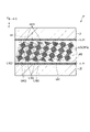
- FIG. 1 is a cross-sectional view showing an example of a liquid crystal element 10 having a transmissive polarization grating TPG.
- FIG. 2 is a cross-sectional view showing an example of a liquid crystal element 20 having a reflective polarization grating RPG.
- FIG. 3 is a cross-sectional view showing a modification of the liquid crystal element 20.
- FIG. 4 is a diagram for explaining the optical action of the transmission-type polarization diffraction grating TPG.
- FIG. 5 is a diagram for explaining the optical action of the reflective polarization diffraction grating RPG.
- FIG. 6 is a cross-sectional view showing a configuration example of the polarization conversion element 1. As shown in FIG. FIG. FIG.
- FIG. 7 is a cross-sectional view showing another configuration example of the polarization conversion element 1.
- FIG. 8 is a cross-sectional view showing another configuration example of the polarization conversion element 1.
- FIG. 9 is a cross-sectional view showing another configuration example of the polarization conversion element 1.
- FIG. 10 is a diagram for explaining the regions A1 to 4A of the polarization diffraction grating RPG.
- FIG. 11 is a cross-sectional view showing another example of the liquid crystal element 20 provided with the polarization diffraction grating RPG.
- FIG. 12 is a cross-sectional view showing another configuration example of the polarization conversion element 1. As shown in FIG. FIG. FIG.
- FIG. 13 is a cross-sectional view showing another configuration example of the polarization conversion element 1.
- FIG. 14 is a diagram schematically showing the polarization diffraction gratings RPG1 to RPG3.
- FIG. 15 is a cross-sectional view showing another configuration example of the polarization conversion element 1.
- FIG. 16 is a cross-sectional view showing another configuration example of the polarization conversion element 1. As shown in FIG.
- X-axis, Y-axis, and Z-axis which are orthogonal to each other, are shown as necessary to facilitate understanding.
- the direction along the X axis is called the X direction or first direction
- the direction along the Y axis is called the Y direction or second direction
- the direction along the Z axis is called the Z direction or third direction.
- a plane defined by the X and Y axes is called the XY plane. Viewing the XY plane is called planar viewing.
- the first direction X and the second direction Y correspond to directions parallel to the main surface of the substrate included in the polarization conversion element
- the third direction Z corresponds to the thickness direction of the polarization conversion element.
- FIG. 1 is a cross-sectional view showing an example of a liquid crystal element 10 having a transmissive polarization grating TPG.
- the liquid crystal element 10 includes a transparent substrate (first transparent substrate) 11, an alignment film AL11, a liquid crystal layer (first liquid crystal layer) LC1, an alignment film AL12, and a transparent substrate 12.
- the transparent substrate 11 faces the transparent substrate 12 in the third direction Z.
- the liquid crystal layer LC1 functions as a polarization diffraction grating TPG and is located between the transparent substrates 11 and 12.
- FIG. 1 is a cross-sectional view showing an example of a liquid crystal element 10 having a transmissive polarization grating TPG.
- the liquid crystal element 10 includes a transparent substrate (first transparent substrate) 11, an alignment film AL11, a liquid crystal layer (first liquid crystal layer) LC1, an alignment film AL12, and a transparent substrate 12.
- the transparent substrate 11 faces the transparent substrate 12 in the third direction Z.
- the liquid crystal layer LC1 functions
- the transparent substrates 11 and 12 are composed of, for example, transparent glass plates or transparent synthetic resin plates.
- the transparent substrate 11 has an inner surface 11A.
- the transparent substrate 12 has an inner surface 12A.
- the inner surfaces 11A and 12A are surfaces parallel to the XY plane.
- the alignment film AL11 is arranged on the inner surface 11A of the transparent substrate 11.
- the alignment film AL12 is arranged on the inner surface 12A of the transparent substrate 12 .
- the alignment film AL12 faces the alignment film AL11 in the third direction Z.
- the alignment films AL11 and AL12 are horizontal alignment films made of, for example, polyimide and having an alignment control force along the XY plane.
- the alignment films AL11 and AL12 are photo-alignment films for forming a spatially varying liquid crystal alignment pattern.
- the liquid crystal layer LC1 is arranged between the alignment films AL11 and AL12 and is in contact with the alignment films AL11 and AL12.
- the liquid crystal layer LC1 has a main surface LS1.
- the main surface LS1 here is, for example, a boundary between the liquid crystal layer LC1 and the alignment film AL12, and a surface parallel to the XY plane.
- the liquid crystal layer LC1 has a thickness d1 along the third direction Z.
- the liquid crystal layer LC1 has nematic liquid crystals aligned along the third direction Z, which is the normal direction of the liquid crystal layer LC1. In one example, the nematic liquid crystals are aligned in the third direction Z as shown.
- the liquid crystal layer LC1 may be oriented such that the liquid crystal molecules LM11 aligned in the third direction Z are slightly twisted.
- the liquid crystal layer LC1 has a plurality of liquid crystal structures LMS1. Focusing on one liquid crystal structure LMS1, the liquid crystal structure LMS1 has a liquid crystal molecule LM11 located on one end side and a liquid crystal molecule LM12 located on the other end side.
- the liquid crystal molecules LM11 are close to the alignment film AL11, and the liquid crystal molecules LM12 are close to the alignment film AL12.
- the orientation direction of the liquid crystal molecules LM11 and the orientation direction of the liquid crystal molecules LM12 are substantially the same.
- the alignment direction of the other liquid crystal molecules LM1 between the liquid crystal molecules LM11 and LM12 also substantially matches the alignment direction of the liquid crystal molecules LM11.
- the orientation directions of the liquid crystal molecules LM1 forming one liquid crystal structure LMS1 are uniform in the third direction Z.
- the alignment direction of the liquid crystal molecules LM1 here corresponds to the direction of the long axis of the liquid crystal molecules on the XY plane.
- the plurality of liquid crystal structures LMS1 are aligned in the first direction X and also aligned in the second direction Y.
- a plurality of liquid crystal structures LMS1 adjacent along the first direction X have different alignment directions.
- the orientation direction of the plurality of liquid crystal molecules LM11 adjacent to the alignment film AL11 and the orientation direction of the plurality of liquid crystal molecules LM12 adjacent to the alignment film AL12 are set along the first direction X such that the long axes of the liquid crystal molecules rotate. is continuously changing to In the liquid crystal layer LC1, the alignment directions of the plurality of liquid crystal structures LMS1 adjacent to each other along the second direction Y are aligned.
- Such a liquid crystal layer LC1 is cured in a state in which the alignment directions of the liquid crystal molecules LM1 including the liquid crystal molecules LM11 and the liquid crystal molecules LM12 are fixed. In other words, the alignment direction of the liquid crystal molecules LM1 is not controlled according to the electric field. Therefore, the liquid crystal element 10 does not have electrodes for alignment control.
- the retardation (phase difference) of the liquid crystal layer LC1 is ⁇ n.
- d1 is preferably set to 1/2 of a specific wavelength (for example, green wavelength) ⁇ .
- the liquid crystal layer LC1 functioning as the polarization diffraction grating TPG is positioned between the pair of transparent substrates 11 and 12, but at least one of the transparent substrates 11 and 12 may be omitted, At least one of the alignment films AL11 and AL12 may be omitted. Also, a plurality of polarization diffraction gratings TPG may be stacked along the third direction Z. FIG.
- FIG. 2 is a cross-sectional view showing an example of a liquid crystal element 20 having a reflective polarization grating RPG.
- the liquid crystal element 20 includes a transparent substrate (second transparent substrate) 21, an alignment film AL21, a liquid crystal layer (second liquid crystal layer) LC2, an alignment film AL22, and a transparent substrate 22.
- the transparent substrate 21 faces the transparent substrate 22 in the third direction Z.
- the liquid crystal layer LC2 functions as a polarization diffraction grating RPG and is positioned between the transparent substrates 21 and 22 .
- the transparent substrates 21 and 22 are composed of, for example, transparent glass plates or transparent synthetic resin plates.
- the transparent substrate 21 has an inner surface 21A.
- the transparent substrate 22 has an inner surface 22A.
- the inner surfaces 21A and 22A are surfaces parallel to the XY plane.
- the alignment film AL21 is arranged on the inner surface 21A of the transparent substrate 21.
- the alignment film AL22 is arranged on the inner surface 22A of the transparent substrate 22 .
- the alignment film AL22 faces the alignment film AL21 in the third Z direction.
- the alignment films AL21 and AL22 are horizontal alignment films made of, for example, polyimide and having an alignment control force along the XY plane.
- the alignment films AL21 and AL22 are photo-alignment films for forming a spatially varying liquid crystal alignment pattern.
- the liquid crystal layer LC2 is arranged between the alignment films AL21 and AL22 and is in contact with the alignment films AL21 and AL22.
- the liquid crystal layer LC2 has a main surface LS2.
- the main surface LS2 here is, for example, a boundary between the liquid crystal layer LC2 and the alignment film AL22, and a surface parallel to the XY plane.
- the liquid crystal layer LC2 has a thickness d2 along the third direction Z.
- the liquid crystal layer LC2 has cholesteric liquid crystal.
- one liquid crystal molecule LM2 among a plurality of liquid crystal molecules positioned on the same plane parallel to the XY plane is shown as the liquid crystal molecule LM2 forming the cholesteric liquid crystal.
- the orientation direction of the liquid crystal molecules LM2 corresponds to the average orientation direction of a plurality of liquid crystal molecules positioned on the same plane.
- the liquid crystal layer LC2 has a plurality of liquid crystal structures LMS2. Focusing on one liquid crystal structure LMS2, the liquid crystal structure LMS2 has a liquid crystal molecule LM21 located on one end side and a liquid crystal molecule LM22 located on the other end side. The liquid crystal molecules LM21 are close to the alignment film AL21, and the liquid crystal molecules LM22 are close to the alignment film AL22. A plurality of liquid crystal molecules LM2 including the liquid crystal molecules LM21 and LM22 are spirally stacked around the spiral axis AX to form a cholesteric liquid crystal. That is, the liquid crystal structure LMS2 corresponds to cholesteric liquid crystal.
- the liquid crystal structure LMS2 has a helical pitch P.
- the helical pitch P indicates one helical period (thickness along the helical axis AX required for the liquid crystal molecules LM2 to rotate 360 degrees).
- the thickness d2 of the liquid crystal layer LC2 is several times the helical pitch P or more.
- the helical axis AX of the liquid crystal structure LMS2 is parallel to the third direction Z, which is the normal direction of the liquid crystal layer LC2.
- the plurality of liquid crystal structures LMS2 are aligned in the first direction X and also aligned in the second direction Y.
- a plurality of liquid crystal structures LMS2 adjacent along the first direction X have different alignment directions.
- the alignment direction of the multiple liquid crystal molecules LM21 aligned along the alignment film AL21 and the alignment direction of the multiple liquid crystal molecules LM22 aligned along the alignment film AL22 change continuously.
- the alignment directions of the plurality of liquid crystal structures LMS2 adjacent to each other along the second direction Y are aligned.
- the liquid crystal layer LC2 has a plurality of reflecting surfaces RS indicated by dashed lines between the alignment films AL21 and AL22.
- the multiple reflective surfaces RS are substantially parallel to each other.
- the reflective surface RS reflects a portion of circularly polarized incident light and transmits other circularly polarized light.
- the reflection surface RS corresponds to a surface in which the alignment directions of the liquid crystal molecules LM2 are aligned or a surface in which spatial phases are aligned (equiphase surface).
- the reflective surface RS is inclined with respect to the main surface LS2 of the liquid crystal layer LC2.
- the liquid crystal structure LMS2 reflects circularly polarized light with the same turning direction as that of the cholesteric liquid crystal out of the light of the specific wavelength ⁇ .
- the rotation direction of the cholesteric liquid crystal is clockwise
- the clockwise circularly polarized light of the light of the specific wavelength ⁇ is reflected, and the counterclockwise circularly polarized light is transmitted.
- the rotation direction of the cholesteric liquid crystal is counterclockwise, the counterclockwise circularly polarized light of the light of the specific wavelength ⁇ is reflected, and the clockwise circularly polarized light is transmitted.
- Such a liquid crystal layer LC2 is cured in a state in which the alignment directions of the liquid crystal molecules LM2 including the liquid crystal molecules LM21 and the liquid crystal molecules LM22 are fixed. In other words, the alignment direction of the liquid crystal molecules LM2 is not controlled according to the electric field. Therefore, the liquid crystal element 20 does not have electrodes for alignment control.
- the selective reflection band ⁇ of the cholesteric liquid crystal for vertically incident light is determined based on the helical pitch P of the cholesteric liquid crystal, the refractive index ne for extraordinary light, and the refractive index no for ordinary light. P”. Therefore, in order to efficiently reflect the circularly polarized light of the specific wavelength ⁇ on the reflecting surface RS, the helical pitch P and the refractive indices ne and no are set so that the specific wavelength ⁇ is included in the selective reflection wavelength band ⁇ . .
- the liquid crystal layer LC2 functioning as the polarization diffraction grating RPG is positioned between the pair of transparent substrates 21 and 22, but at least one of the transparent substrates 21 and 22 may be omitted, At least one of the alignment films AL21 and AL22 may be omitted. Also, a plurality of polarization diffraction gratings RPG may be stacked along the third direction Z. FIG.
- FIG. 3 is a cross-sectional view showing a modification of the liquid crystal element 20. As shown in FIG. 3 is different from the example shown in FIG. 2 in that the helical axis AX of the liquid crystal structure LMS2 is inclined with respect to the normal direction (third direction Z) of the liquid crystal layer LC2. are different.
- the multiple liquid crystal structures LMS2 adjacent along the first direction X have different alignment directions.
- the alignment direction of the multiple liquid crystal molecules LM21 aligned along the alignment film AL21 and the alignment direction of the multiple liquid crystal molecules LM22 aligned along the alignment film AL22 change continuously.
- the liquid crystal layer LC2 has a plurality of reflecting surfaces RS indicated by dashed lines between the alignment films AL21 and AL22.
- the multiple reflective surfaces RS are substantially parallel to each other. According to Bragg's law, the reflective surface RS reflects a portion of circularly polarized incident light and transmits other circularly polarized light. In the XZ cross section shown in FIG. 3, the reflective surface RS is inclined with respect to the main surface LS2 of the liquid crystal layer LC2.
- FIG. 4 is a diagram for explaining the optical action of the transmission-type polarization diffraction grating TPG.
- the polarization grating TPG is divided into the first circularly polarized light C1 and the second circularly polarized light C1 of the light NP.
- the two circularly polarized light beams C2 are respectively diffracted.
- the second circularly polarized light C2 is circularly polarized light having a rotation opposite to that of the first circularly polarized light C1.
- the second circularly polarized light C2 is diffracted in a direction different from that of the first circularly polarized light C1.
- the first circularly polarized light C1 is diffracted diagonally to the right from the polarization grating TPG
- the second circularly polarized light C2 is diffracted diagonally to the left from the polarization grating TPG. That is, when the unpolarized light NP is the incident light, the polarization grating TPG separates the light NP into the first circularly polarized light C1 and the second circularly polarized light C2.
- the polarization diffraction grating TPG converts the first circularly polarized light C1 into the second circularly polarized light C2. Transform and diffract.
- the first circularly polarized light C1 incident obliquely to the right toward the polarization grating TPG is converted into the second circularly polarized light C2 and diffracted in the normal direction of the polarization grating TPG.
- the polarization grating TPG converts the second circularly polarized light C2 into the first circularly polarized light C1. Transform and diffract.
- the second circularly polarized light C2 incident obliquely to the left toward the polarization grating TPG is converted into the first circularly polarized light C1 and diffracted in the normal direction of the polarization grating TPG. That is, when the incident light is circularly polarized light, the polarization diffraction grating TPG diffracts the transmitted light while converting it into reverse circularly polarized light.
- FIG. 5 is a diagram for explaining the optical action of the reflective polarization diffraction grating RPG.
- the polarization grating RPG reflects the first circularly polarized light C1 of the light NP.
- the second circularly polarized light C2 is transmitted while being reflected by the surface RS.
- the first circularly polarized light C1 is obliquely reflected at the inclined reflecting surface RS.
- the second circularly polarized light C2 passes through the reflecting surface RS and travels straight in the normal direction of the polarization diffraction grating RPG.
- the polarization diffraction grating RPG As shown on the right side of FIG. 5, when unpolarized light NP as incident light is incident on the polarization diffraction grating RPG from an oblique direction, the polarization diffraction grating RPG The polarized light C1 is reflected by the reflecting surface RS, and the second circularly polarized light C2 is transmitted. The first circularly polarized light C1 is reflected in the normal direction at the inclined reflective surface RS. The second circularly polarized light C2 passes through the reflecting surface RS and travels straight in an oblique direction with respect to the polarization diffraction grating RPG.
- the polarization conversion element 1 Several configuration examples of the polarization conversion element 1 will be described below.
- the first circularly polarized light and the second circularly polarized light separated by the transmissive polarization grating TPG are denoted by C10 and C20, respectively, and the circularly polarized lights on the optical path of the first circularly polarized light C10 are denoted by C11 and C12. , C13 .
- the circularly polarized light described here may be strictly circularly polarized light, or may be circularly polarized light approximating elliptically polarized light.
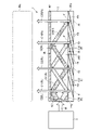
- FIG. 6 is a cross-sectional view showing a configuration example of the polarization conversion element 1.
- the polarization conversion element 1 includes a light guide plate (first light guide plate) 3 and a transmissive polarization diffraction grating (first polarization diffraction grating) TPG.
- the light guide plate 3 has a first main surface 3A, a second main surface 3B opposite to the first main surface 3A, and side surfaces 3C.
- the light guide plate 3 is made of, for example, a transparent glass plate or a transparent synthetic resin plate.
- the side surface 3C is a surface formed along the thickness direction of the light guide plate 3 .
- the polarization diffraction grating TPG faces the side surface 3C.
- the polarization diffraction grating TPG here corresponds to the liquid crystal layer LC1 in the liquid crystal element 10 shown in FIG.
- the liquid crystal element 10 shown in FIG. 1 may face the side surface 3C, and in this case, the transparent substrate 11 is adhered to the side surface 3C.
- the transparent substrate 12 and the alignment film AL12 of the liquid crystal element 10 shown in FIG. 1 may be omitted, and the main surface LS1 of the liquid crystal layer LC1 may be adhered to the side surface 3C.
- the liquid crystal layer LC1 is arranged between the light guide plate 3 and the transparent substrate 11.
- a normal line 3CN of the side surface 3C coincides with the third direction Z shown in FIG. That is, the polarization grating TPG has nematic liquid crystals oriented along the normal 3CN of the side surface 3C.
- a plurality of liquid crystal molecules LM1 forming the liquid crystal structure LMS1 shown in FIG. 1 are aligned along the normal 3CN, and the orientation directions of these liquid crystal molecules LM1 are uniform along the normal 3CN. , as described above, may be slightly twisted.
- the first main surface 3A of the light guide plate 3 is in contact with a low refractive index medium having a lower refractive index than the light guide plate 3.
- the low refractive index medium is, for example, the thin film 4, but may also be air.
- the thin film 4 may be a reflective layer made of a highly reflective material. As will be described later, such a first main surface 3A forms an interface that totally reflects light diffracted by the polarization diffraction grating TPG.
- the light source 5 faces the polarization diffraction grating TPG.
- An optical system including various lenses may be arranged between the light source 5 and the polarization diffraction grating TPG.
- the light source 5 is configured to emit unpolarized light NP toward the polarization grating TPG.
- the light NP emitted from the light source 5 is separated into a first circularly polarized light C10 and a second circularly polarized light C20 at the polarization diffraction grating TPG.
- the first circularly polarized light C10 is right-handed circularly polarized light (R)
- the second circularly polarized light C20 is left-handed circularly polarized light (L).
- the second circularly polarized light C20 is diffracted toward the second main surface 3B of the light guide plate 3 at the polarization diffraction grating TPG.
- the first circularly polarized light C10 is diffracted toward the first main surface 3A of the light guide plate 3 at the polarization diffraction grating TPG.
- the first circularly polarized light C10 that has reached the first main surface 3A at an incident angle equal to or greater than the critical angle is totally reflected at the interface between the light guide plate 3 and the thin film 4 .
- the s-polarized component and the p-polarized component included in the first circularly polarized light C10 are each phase-shifted.
- the totally reflected light C11 is converted into circularly polarized light having a direction opposite to that of the first circularly polarized light C10. That is, the light C11 is counterclockwise circularly polarized light, like the second circularly polarized light C20.
- Such second circularly polarized light C20 and light C11 can be transmitted through the second main surface 3B and can form illumination light with substantially uniform polarization states.
- the polarization conversion element 1 described here it is possible to convert the non-polarized light NP emitted from the light source 5 into light (circularly polarized light) with almost the same polarization state with almost no loss. It is possible to improve the light utilization efficiency.
- a display panel (for example, a liquid crystal panel) PNL which is an example of an illumination target, is arranged so as to overlap the second main surface 3B, as indicated by the dotted line, and is illuminated by illumination light transmitted through the second main surface 3B.
- the polarization conversion element 1, together with the light source 5, can constitute an illumination device IL.
- the polarization conversion element 1, the light source 5, and the display panel PNL can constitute a display device DSP.
- FIG. 7 is a cross-sectional view showing another configuration example of the polarization conversion element 1.
- the polarization conversion element 1 is different from the example shown in FIG. grating) TPG2 and a retardation plate RT.
- the polarization diffraction grating TPG1 facing the side surface 3C is the same as the polarization diffraction grating TPG shown in FIG. 6, and the description thereof is omitted.
- the polarization diffraction grating TPG2 faces the second main surface 3B.
- the polarization diffraction grating TPG2 here corresponds to the liquid crystal layer LC1 of the liquid crystal element 10 shown in FIG.
- the liquid crystal element 10 shown in FIG. 1 may face the second main surface 3B, and in this case, the transparent substrate 11 is adhered to the second main surface 3B.
- the transparent substrate 12 and the alignment film AL12 of the liquid crystal element 10 shown in FIG. 1 may be omitted, and the main surface LS1 of the liquid crystal layer LC1 may be adhered to the second main surface 3B.
- the liquid crystal layer LC1 is arranged between the light guide plate 3 and the transparent substrate 11.
- the normal 3BN of the second main surface 3B matches the third direction Z shown in FIG. That is, the polarization diffraction grating TPG2 has nematic liquid crystal aligned along the normal 3BN of the second main surface 3B.
- a plurality of liquid crystal molecules LM1 forming the liquid crystal structure LMS1 shown in FIG. 1 are aligned along the normal 3BN, and the alignment direction of these liquid crystal molecules LM1 is uniform along the normal 3BN. , as described above, may be slightly twisted.
- the polarization diffraction grating TPG2 may be configured to have a converging or diverging lens action by adjusting the phase distribution according to the alignment state of the liquid crystal molecules.
- the retardation plate RT faces the polarization diffraction grating TPG2.
- the retardation plate RT may be adhered to the polarization diffraction grating TPG2, or an air layer may be interposed between the retardation plate RT and the polarization diffraction grating TPG2.
- the retardation plate RT is a 1/4 wavelength plate, and gives a phase difference of 1/4 wavelength to the transmitted light.
- the retardation plate RT gives, for example, a phase difference of 1/4 wavelength to light of a specific wavelength, but it is not limited to this.
- the retardation plate RT it is possible to apply a broadband retardation plate that imparts a phase difference of approximately 1/4 wavelength to light of each wavelength in the visible light range.
- the light NP emitted from the light source 5 is separated into a first circularly polarized light C10 and a second circularly polarized light C20 at the polarization diffraction grating TPG1.
- the first circularly polarized light C10 is right-handed circularly polarized light (R)
- the second circularly polarized light C20 is left-handed circularly polarized light (L).
- the first circularly polarized light C10 is diffracted toward the first main surface 3A of the light guide plate 3 at the polarization diffraction grating TPG1.
- the light C11 totally reflected by the first main surface 3A is converted into circularly polarized light having a direction opposite to that of the first circularly polarized light C10. That is, the light C11 is counterclockwise circularly polarized light.
- the light C11 is diffracted in the direction along the normal 3BN at the polarization diffraction grating TPG2, and converted into circularly polarized light having a direction opposite to that of the light C11. That is, the light C12 diffracted by the polarization diffraction grating TPG2 is clockwise circularly polarized light.
- Light C12 is converted into light C13, which is linearly polarized light (PL), at the retardation plate RT.
- the second circularly polarized light C20 is diffracted toward the second main surface 3B of the light guide plate 3 at the polarization diffraction grating TPG1.
- the second circularly polarized light C20 is diffracted in the direction along the normal 3BN at the polarization diffraction grating TPG2, and converted into circularly polarized light having a direction opposite to that of the second circularly polarized light C20. That is, the light C21 diffracted by the polarization diffraction grating TPG2 is clockwise circularly polarized light.
- Light C21 is converted into light C22, which is linearly polarized light (PL), at the retardation plate RT.
- Such light C12 and light C22 can form linearly polarized illumination light with generally aligned polarization axes.
- the display panel PNL which is an example of an illumination target, is arranged so as to overlap the retardation plate RT, and is illuminated by illumination light transmitted through the retardation plate RT.
- a polarization conversion element 1 it is possible to convert the non-polarized light NP emitted from the light source 5 into light (linearly polarized light) having a generally uniform polarization state, thereby improving the light utilization efficiency. be able to.
- FIG. 8 is a cross-sectional view showing another configuration example of the polarization conversion element 1.
- the polarization conversion element 1 in comparison with the example shown in FIG. 6, in addition to the light guide plate 3 and the transmissive polarization diffraction grating TPG, the polarization conversion element 1 includes a reflection polarization diffraction grating RPG and a retardation plate. RT and are different in that they are provided.
- the polarization diffraction grating TPG faces the side surface 3C.
- the polarization diffraction grating TPG here corresponds to the liquid crystal layer LC1 in the liquid crystal element 10 shown in FIG.
- the liquid crystal element 10 shown in FIG. 1 may face the side surface 3C, and in this case, the transparent substrate 11 is adhered to the side surface 3C.
- the transparent substrate 12 and the alignment film AL12 of the liquid crystal element 10 shown in FIG. 1 may be omitted, and the main surface LS1 of the liquid crystal layer LC1 may be adhered to the side surface 3C.
- the liquid crystal layer LC1 is arranged between the light guide plate 3 and the transparent substrate 11.
- a normal line 3CN of the side surface 3C coincides with the third direction Z shown in FIG. That is, the polarization grating TPG has nematic liquid crystals oriented along the normal 3CN of the side surface 3C.
- a plurality of liquid crystal molecules LM1 forming the liquid crystal structure LMS1 shown in FIG. 1 are aligned along the normal 3CN, and the orientation directions of these liquid crystal molecules LM1 are uniform along the normal 3CN. , as described above, may be slightly twisted.
- the polarization diffraction grating RPG faces the first main surface 3A.
- the polarization diffraction grating RPG here corresponds to, for example, the liquid crystal layer LC2 of the liquid crystal element 20 shown in FIG.
- the liquid crystal element 20 shown in FIG. 2 may face the first main surface 3A, and in this case, the transparent substrate 21 is adhered to the first main surface 3A.
- the transparent substrate 22 and the alignment film AL22 of the liquid crystal element 20 shown in FIG. 2 may be omitted, and the main surface LS2 of the liquid crystal layer LC2 may be adhered to the first main surface 3A.
- the liquid crystal layer LC2 is arranged between the light guide plate 3 and the transparent substrate 21.
- the normal 3AN of the first main surface 3A coincides with the third direction Z shown in FIG. That is, the polarization diffraction grating RPG has cholesteric liquid crystals CL, and the spiral axis AX of the cholesteric liquid crystals CL is substantially parallel to the normal line 3AN of the first main surface 3A.
- the polarization grating RPG is the liquid crystal layer LC2 of the liquid crystal element 20 shown in FIG. 3
- the helical axis AX of the cholesteric liquid crystal CL is inclined with respect to the normal 3AN.
- the polarization diffraction grating RPG has a reflecting surface RS inclined with respect to the first main surface 3A.
- the cholesteric liquid crystal CL is schematically shown on the right side of the figure.
- the cholesteric liquid crystal CL is spiraled to reflect right-handed circularly polarized light of a particular wavelength ⁇ and has a helical pitch P along the helical axis AX.
- the helical pitch P is constant with little change along the helical axis AX.
- the retardation plate RT faces the second main surface 3B.
- the retardation plate RT may be adhered to the light guide plate 3 , or an air layer may be interposed between the retardation plate RT and the light guide plate 3 .
- the retardation plate RT is a 1/4 wavelength plate, and gives a phase difference of 1/4 wavelength to the transmitted light.
- the non-polarized light NP emitted from the light source 5 is separated into a first circularly polarized light C10 and a second circularly polarized light C20 at the polarization diffraction grating TPG.
- the first circularly polarized light C10 is right-handed circularly polarized light (R)
- the second circularly polarized light C20 is left-handed circularly polarized light (L).
- the first circularly polarized light C10 is diffracted toward the first main surface 3A of the light guide plate 3 at the polarization diffraction grating TPG.
- the diffracted first circularly polarized light C10 is transmitted through the first main surface 3A and reflected in the direction along the normal 3AN on the reflecting surface RS of the polarization diffraction grating RPG.
- the reflected light C11 is a clockwise circularly polarized light similar to the first circularly polarized light C10.
- the light C11 is transmitted through the second principal surface 3B and converted into the light C12, which is linearly polarized light (PL), by the retardation plate RT.
- the second circularly polarized light C20 is diffracted toward the second main surface 3B of the light guide plate 3 at the polarization diffraction grating TPG.
- the second circularly polarized light C20 that has reached the second main surface 3B at an incident angle equal to or greater than the critical angle is totally reflected at the interface between the light guide plate 3 and the retardation plate RT.
- the totally reflected light C21 is converted into circularly polarized light having a direction opposite to that of the second circularly polarized light C20. That is, the light C21 is clockwise circularly polarized light.
- the light C21 is transmitted through the first main surface 3A and reflected in the direction along the normal 3AN on the reflecting surface RS of the polarization diffraction grating RPG.
- the reflected light C22 is right-handed circularly polarized light, similar to light C21.
- the light C22 is transmitted through the second main surface 3B and converted into light C23, which is linearly polarized light (PL
- Such light C12 and light C23 can form linearly polarized illumination light with generally aligned polarization axes.
- the display panel PNL which is an example of an illumination target, is arranged so as to overlap the retardation plate RT, and is illuminated by illumination light transmitted through the retardation plate RT.
- a polarization conversion element 1 it is possible to convert the non-polarized light NP emitted from the light source 5 into light (linearly polarized light) having a generally uniform polarization state, thereby improving the light utilization efficiency. be able to.
- a light diffusion sheet, a prism sheet, a polarizer, or the like may be arranged between the retardation plate RT and the display panel PNL.
- FIG. 9 is a cross-sectional view showing another configuration example of the polarization conversion element 1. As shown in FIG. The example shown in FIG. 9 differs from the example shown in FIG. 8 in that the polarization grating RPG has a thickness distribution.
- the polarization diffraction grating RPG has multiple areas A1 to A4.
- the area A1 first area is located on the side close to the polarization diffraction grating TPG or the light source 5 .
- the area A2 second area is positioned away from the polarization grating TPG, and the area A1 is positioned between the polarization grating TPG and the area A2.
- Area A2 is located between area A1 and area A3, and area A3 is located between area A2 and area A4. That is, the areas A1 to A4 are arranged in order toward the side away from the polarization diffraction grating TPG. The thickness relationships of these regions A1 to A4 will be described below.
- FIG. 10 is a diagram for explaining the regions A1 to 4A of the polarization diffraction grating RPG.
- a region A1 is a region having cholesteric liquid crystal CL1 and has a thickness T1.
- a region A2 is a region having cholesteric liquid crystal CL2 and has a thickness T2.
- a region A3 is a region having cholesteric liquid crystal CL3 and has a thickness T3.
- a region A4 is a region having cholesteric liquid crystal CL4 and has a thickness T4.
- the thickness here is, for example, the length along the normal 3AN of the first main surface 3A with which the polarization diffraction grating RPG is in contact.
- the thickness T1 of the region A1 is smaller than the thickness T2 of the region A2, the thickness T2 of the region A2 is smaller than the thickness T3 of the region A3, and the thickness T3 of the region A3 is smaller than the thickness T4 of the region A4 (T1 ⁇ T2 ⁇ T3 ⁇ T4).
- Each of the cholesteric liquid crystals CL1 to CL4 has the same helical pitch P.
- the length L1 along the helical axis AX of the cholesteric liquid crystal CL1 is substantially equal to the thickness T1 and is denoted as P*N1.
- the length L2 of the cholesteric liquid crystal CL2 is substantially equal to the thickness T2 and is denoted as P*N2.
- the length L3 of the cholesteric liquid crystal CL3 is substantially equal to the thickness T3 and is denoted as P*N3.
- the length L4 of the cholesteric liquid crystal CL4 is substantially equal to the thickness T4 and is denoted as P*N4.
- N1 to N4 are 10 or less, for example.
- N1 is smaller than N2, N2 is smaller than N3, and N3 is smaller than N4 (N1 ⁇ N2 ⁇ N3 ⁇ N4).
- the length L1 is smaller than the length L2, the length L2 is smaller than the length L3, and the length L3 is smaller than the length L4 (L1 ⁇ L2 ⁇ L3 ⁇ L4).
- the coefficients (N1 to N4) are in the range of, for example, 10 or less, the larger the coefficient, the higher the reflectance tends to be. Therefore, the reflectance of the cholesteric liquid crystal CL2 in the area A2 is higher than the reflectance of the cholesteric liquid crystal CL1 in the area A1. Similarly, the reflectance of area A3 is higher than that of area A2, and the reflectance of area A4 is higher than that of area A3.
- the non-polarized light NP emitted from the light source 5 is separated into a first circularly polarized light C10 and a second circularly polarized light C20 at the polarization diffraction grating TPG.
- the first circularly polarized light C10 is right-handed circularly polarized light (R)
- the second circularly polarized light C20 is left-handed circularly polarized light (L).
- the first circularly polarized light C10 is diffracted toward the first main surface 3A of the light guide plate 3 at the polarization diffraction grating TPG. Part of the diffracted first circularly polarized light C10 is reflected in the direction along the normal 3AN on the reflecting surface RS formed in the area A1 of the polarization diffraction grating RPG.
- the reflected light C11 is right-handed circularly polarized light similar to the first circularly polarized light C10, and is converted into linearly polarized light (PL) at the retardation plate RT.
- the diffracted first circularly polarized light C10 are totally reflected and converted into circularly polarized light having a direction opposite to that of the first circularly polarized light C10. That is, the totally reflected light C12 is counterclockwise circularly polarized light.
- the light C12 is totally reflected by the second main surface 3B and converted into circularly polarized light having a direction opposite to that of the light C12. That is, the totally reflected light C13 is clockwise circularly polarized light.
- Part of the light C13 is reflected in a direction along the normal line 3AN at the reflecting surface RS formed in the area A3 of the polarization grating RPG.
- the reflected light C14 is right-handed circularly polarized light and is converted into linearly polarized light (PL) at the retardation plate RT.
- the second circularly polarized light C20 is diffracted toward the second main surface 3B of the light guide plate 3 at the polarization diffraction grating TPG.
- the diffracted second circularly polarized light C20 is totally reflected by the second main surface 3B and converted into circularly polarized light having a direction opposite to that of the second circularly polarized light C20. That is, the totally reflected light C21 is clockwise circularly polarized light.
- Part of the light C21 is reflected in a direction along the normal 3AN on the reflecting surface RS formed in the area A2 of the polarization diffraction grating RPG.
- the reflected light C22 is right-handed circularly polarized light and is converted into linearly polarized light (PL) at the retardation plate RT.
- the light C21 are totally reflected and converted into circularly polarized light having a direction opposite to that of the light C21. That is, the totally reflected light C23 is converted into counterclockwise circularly polarized light.
- the light C23 is totally reflected by the second main surface 3B and converted into circularly polarized light having a direction opposite to that of the light C23. That is, the totally reflected light C24 is clockwise circularly polarized light.
- Part of the light C24 is reflected in the direction along the normal 3AN at the reflecting surface RS formed in the area A4 of the polarization grating RPG.
- the reflected light C25 is right-handed circularly polarized light and is converted into linearly polarized light (PL) at the retardation plate RT.
- FIG. 11 is a cross-sectional view showing another example of the liquid crystal element 20 provided with the polarization diffraction grating RPG.
- a liquid crystal layer LC2 corresponding to the polarization diffraction grating RPG has a plurality of liquid crystal structures (cholesteric liquid crystals) LMS2.
- a plurality of liquid crystal molecules LM2 forming the liquid crystal structure LMS2 are cured with their alignment directions fixed.
- the liquid crystal layer LC2 has a plurality of reflecting surfaces RS indicated by dotted lines between the alignment films AL21 and AL22.
- the reflecting surface RS is a curved surface, concave on the side facing the transparent substrate 22 and convex on the side facing the transparent substrate 21 .
- the reflecting surface RS may be convex toward the side facing the transparent substrate 22 .
- Such a liquid crystal element 20 has a lens action of reflecting a part of the circularly polarized light of the incident light and converging or diverging it on the reflecting surface RS.
- FIG. 12 is a cross-sectional view showing another configuration example of the polarization conversion element 1.
- the polarization conversion element 1 includes the polarization diffraction grating RPG shown in FIG. Description of each part is omitted.
- the light on each optical path is given the same reference numerals as in the example shown in FIG. 9, and detailed description thereof is omitted.
- a part of the first circularly polarized light C10 is reflected by the reflecting surface RS of the polarization diffraction grating RPG and diverges under the lens action of the polarization diffraction grating RPG.
- a portion of the light C13, a portion of the light C21, and a portion of the light C24, which are circularly polarized light similar to the first circularly polarized light C10, are each reflected on the reflecting surface RS and diverged.
- the shape of the reflecting surface RS it is possible to reflect and converge circularly polarized light similar to the first circularly polarized light C10.
- FIG. 13 is a cross-sectional view showing another configuration example of the polarization conversion element 1.
- the polarization conversion element 1 includes a plurality of reflective polarization gratings RPG1 in addition to the transmission type polarization grating (first polarization grating) TPG. , RPG2, and RPG3.
- the polarization grating (second polarization grating) RPG1 has a reflecting surface RS1
- the polarization grating (third polarization grating) RPG2 has a reflecting surface RS2
- the polarization grating RPG3 has a reflecting surface RS3.
- the inclination angles ⁇ 1 to ⁇ 3 of each of the reflecting surfaces RS1 to RS3 with respect to the plane parallel to the first main surface 3A are substantially the same.
- the polarization diffraction grating RPG2 faces the polarization diffraction grating RPG1 and is arranged between the polarization diffraction grating RPG1 and the light guide plate 3.
- the polarization diffraction grating RPG3 faces the polarization diffraction grating RPG2 and is arranged between the polarization diffraction grating RPG2 and the light guide plate 3 .
- Polarization diffraction grating RPG3 is in contact with first main surface 3A.
- the polarization diffraction grating RPG1, the polarization diffraction grating RPG2, and the polarization diffraction grating RPG3 are laminated along the normal line 3AN. Note that the stacking order of the polarization diffraction grating RPG1, the polarization diffraction grating RPG2, and the polarization diffraction grating RPG3 is not limited to the illustrated example.
- the polarization diffraction grating RPG1, the polarization diffraction grating RPG2, and the polarization diffraction grating RPG3 are equivalent to the liquid crystal element 20 described with reference to FIGS.
- the helical pitches of the polarization diffraction grating RPG1, the polarization diffraction grating RPG2, and the polarization diffraction grating RPG3 are different from each other. This point will be described below.
- FIG. 14 is a diagram schematically showing the polarization diffraction gratings RPG1 to RPG3.
- Polarization grating RPG1 is configured to reflect the first circularly polarized light at the red wavelength.
- Cholesteric liquid crystal CL1 included in polarization grating RPG1 has a helical pitch P1 along helical axis AX1.
- the helical pitch P1 is optimized to correspond to red wavelengths.
- Such cholesteric liquid crystal CL1 forms the reflecting surface RS1 shown in FIG.
- the polarization grating RPG2 is configured to reflect the first circularly polarized light of the green wavelength. That is, the turning direction of the cholesteric liquid crystal CL2 included in the polarization diffraction grating RPG2 is the same as the turning direction of the cholesteric liquid crystal CL1. Further, the helical axis AX2 of the cholesteric liquid crystal CL2 is substantially parallel to the helical axis AX1 of the cholesteric liquid crystal CL1.
- the cholesteric liquid crystal CL2 has a helical pitch P2 along the helical axis AX2. The helical pitch P2 is smaller than the helical pitch P1 (P2 ⁇ P1). The helical pitch P2 is optimized to correspond to the green wavelength.
- Such cholesteric liquid crystal CL2 forms the reflecting surface RS2 shown in FIG.
- the polarization grating RPG3 is configured to reflect the first circularly polarized light of blue wavelength. That is, the turning direction of the cholesteric liquid crystal CL3 included in the polarization diffraction grating RPG3 is the same as the turning direction of the cholesteric liquid crystal CL2. Further, the helical axis AX3 of the cholesteric liquid crystal CL3 is substantially parallel to the helical axis AX2 of the cholesteric liquid crystal CL2.
- the cholesteric liquid crystal CL3 has a helical pitch P3 along the helical axis AX3. The helical pitch P3 is smaller than the helical pitch P2 (P3 ⁇ P2). The helical pitch P3 is optimized for blue wavelengths.
- Such cholesteric liquid crystal CL3 forms the reflecting surface RS3 shown in FIG.
- the light source 5 emits unpolarized light NP toward the polarization grating TPG.
- the light NP includes components of red wavelength ( ⁇ R), green wavelength ( ⁇ G), and blue wavelength ( ⁇ B).
- the light NP is separated into the first circularly polarized light C10 and the second circularly polarized light C20 at the polarization diffraction grating TPG, but only the first circularly polarized light C10 diffracted toward the first principal surface 3A is shown here.
- the first circularly polarized light C10 is, for example, clockwise circularly polarized light.
- the longer the wavelength the larger the diffraction angle with respect to the normal 3CN of the first circularly polarized light C10 diffracted by the polarization diffraction grating TPG. Therefore, the first circularly polarized light RC10 of the red wavelength is diffracted at a larger diffraction angle than the first circularly polarized light GC10 of the green wavelength. Also, the green wavelength first circularly polarized light GC10 is diffracted at a larger diffraction angle than the blue wavelength first circularly polarized light BC10.
- the first circularly polarized light RC10 passes through the polarization gratings RPG3 and RPG2 and is reflected by the reflecting surface RS1 of the polarization grating RPG1.
- the first circularly polarized light GC10 passes through the polarization grating RPG3 and is reflected by the reflecting surface RS2 of the polarization grating RPG2.
- the first circularly polarized light BC10 is reflected at the reflecting surface RS3 of the polarization grating RPG3.
- the inclination angles ⁇ 1 to ⁇ 3 of the reflecting surfaces RS1 to RS3 are substantially the same, the light RC11 reflected by the reflecting surface RS1, the light GC11 reflected by the reflecting surface RS2, and the reflecting surface RS3
- the reflected light BC11 is transmitted through the second main surface 3B at different angles with respect to the normal 3BN of the second main surface 3B.
- Light RC11, light GC11, and light BC11 are clockwise circularly polarized light similar to the first circularly polarized light, and are converted into linearly polarized light (PL) by the retardation plate RT.
- FIG. 15 is a cross-sectional view showing another configuration example of the polarization conversion element 1. As shown in FIG. The example shown in FIG. 15 differs from the example shown in FIG. 13 in that the inclination angles ⁇ 1 to ⁇ 3 of the reflecting surfaces RS1 to RS3 are different from each other.
- the tilt angle ⁇ 1 of the reflecting surface RS1 is smaller than the tilt angle ⁇ 2 of the reflecting surface RS2 ( ⁇ 1 ⁇ 2).
- the tilt angle ⁇ 2 of the reflecting surface RS2 is smaller than the tilt angle ⁇ 3 of the reflecting surface RS3 ( ⁇ 2 ⁇ 3).
- the cholesteric liquid crystal CL1 included in the polarization diffraction grating RPG1, the cholesteric liquid crystal CL2 included in the polarization diffraction grating RPG2, and the cholesteric liquid crystal CL3 included in the polarization diffraction grating RPG3 are as described with reference to FIG. .
- the unpolarized light NP emitted from the light source 5 is separated into the first circularly polarized light C10 and the second circularly polarized light C20 at the polarization diffraction grating TPG, and is diffracted here toward the first main surface 3A. Only the first circular polarization C10 is shown.
- the first circularly polarized light C10 is, for example, clockwise circularly polarized light.
- the red wavelength first circularly polarized light RC10 is reflected at the reflecting surface RS1 of the polarization grating RPG1.
- the green wavelength first circularly polarized light GC10 is reflected at the reflective surface RS2 of the polarization grating RPG2.
- the blue wavelength first circularly polarized light BC10 is reflected at the reflective surface RS3 of the polarization grating RPG3.
- the inclination angles ⁇ 1 to ⁇ 3 of the reflecting surfaces RS1 to RS3 make the light RC11 reflected by the reflecting surface RS1, the light GC11 reflected by the reflecting surface RS2, and the light BC11 reflected by the reflecting surface RS3 substantially the same. It is set to reflect in the direction. That is, each of the light RC11, the light GC11, and the light BC11 is transmitted through the second main surface 3B at substantially the same angle with respect to the normal 3BN of the second main surface 3B.
- Light RC11, light GC11, and light BC11 are clockwise circularly polarized light similar to the first circularly polarized light, and are converted into linearly polarized light (PL) by the retardation plate RT.
- chromatic aberration can be reduced compared to the example shown in FIG. Therefore, it is possible to form illumination light with little color unevenness.
- FIG. 16 is a cross-sectional view showing another configuration example of the polarization conversion element 1.
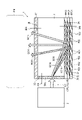
- the polarization conversion element 1 includes light guide plates 31 to 33, transmission-type polarization diffraction gratings TPG1 to TPG3, reflection-type polarization diffraction gratings RPG1 to RPG3, and a retardation plate RT.
- the polarization diffraction grating RPG1 has a reflecting surface RS1 facing the first main surface 31A of the light guide plate 31 and inclined at an inclination angle ⁇ 1 with respect to the first main surface 31A.
- the polarization diffraction grating RPG2 has a reflecting surface RS2 facing the second main surface 31B of the light guide plate 31 and the first main surface 32A of the light guide plate 32 and inclined at an inclination angle ⁇ 2 with respect to the first main surface 32A.
- the polarization diffraction grating RPG3 has a reflecting surface RS3 facing the second main surface 32B of the light guide plate 32 and the first main surface 33A of the light guide plate 33 and inclined at an inclination angle ⁇ 3 with respect to the first main surface 33A. there is These tilt angles ⁇ 1 to ⁇ 3 are different from each other and are set as described with reference to FIG.
- the polarization diffraction grating TPG1 faces the side surface 31C of the light guide plate 31
- the polarization diffraction grating TPG2 faces the side surface 32C of the light guide plate 32
- the polarization diffraction grating TPG3 faces the side surface 33C of the light guide plate 33.
- a common polarization diffraction grating TPG may be arranged on the side surface 31C, the side surface 32C, and the side surface 33C.
- the polarization diffraction gratings TPG1 to TPG3 separate the unpolarized light into the first circularly polarized light and the second circularly polarized light, respectively, but only the first circularly polarized light is illustrated and the description of the second circularly polarized light is omitted.
- the light source 51 faces the polarization diffraction grating TPG1 and is configured to emit unpolarized light NP1 of red wavelength ( ⁇ R) toward the polarization diffraction grating TPG1.
- the light source 52 faces the polarization diffraction grating TPG2 and is configured to emit green wavelength ( ⁇ G) unpolarized light NP2 toward the polarization diffraction grating TPG2.
- the light source 53 is configured to face the polarization diffraction grating TPG3 and emit unpolarized light NP3 of blue wavelength ( ⁇ B) toward the polarization diffraction grating TPG3.
- the first circularly polarized light RC10 of the light NP1 is diffracted toward the first main surface 31A by the polarization diffraction grating TPG1.
- the first circularly polarized light RC10 is reflected at the reflective surface RS1 of the polarization grating RPG1.
- the light RC11 reflected by the reflecting surface RS1 passes through the polarization diffraction grating RPG2, the light guide plate 32, the polarization diffraction grating RPG3, and the light guide plate 33, and is converted into linearly polarized light by the retardation plate RT.
- the first circularly polarized light GC10 of the light NP2 is diffracted toward the first main surface 32A by the polarization diffraction grating TPG2.
- the first circularly polarized light GC10 is reflected at the reflecting surface RS2 of the polarization grating RPG2.
- the light GC11 reflected by the reflecting surface RS2 passes through the polarization diffraction grating RPG3 and the light guide plate 33, and is converted into linearly polarized light by the retardation plate RT.
- the first circularly polarized light BC10 of the light NP3 is diffracted toward the first main surface 33A by the polarization diffraction grating TPG3.
- the first circularly polarized light BC10 is reflected at the reflecting surface RS3 of the polarization grating RPG3.
- the light BC11 reflected by the reflecting surface RS3 is converted into linearly polarized light by the retardation plate RT.
Landscapes
- Physics & Mathematics (AREA)
- General Physics & Mathematics (AREA)
- Optics & Photonics (AREA)
- Nonlinear Science (AREA)
- Chemical & Material Sciences (AREA)
- Crystallography & Structural Chemistry (AREA)
- Mathematical Physics (AREA)
- Spectroscopy & Molecular Physics (AREA)
- Polarising Elements (AREA)
- Diffracting Gratings Or Hologram Optical Elements (AREA)
Abstract
Le but du présent mode de réalisation est d'améliorer l'efficacité d'utilisation de la lumière. Selon un mode de réalisation, un élément de conversion de polarisation comprend : une première plaque de guidage de lumière ayant une première surface principale, une seconde surface principale sur le côté inverse à partir de la première surface principale, et une surface latérale ; un premier réseau de diffraction de polarisation de type transmission faisant face à la surface latérale ; et un second réseau de diffraction de polarisation de type réflexion faisant face à la première surface principale. Le premier réseau de diffraction de polarisation a un cristal liquide nématique orienté le long de la direction normale de la surface latérale, et est configuré pour diffracter une première lumière à polarisation circulaire à l'extérieur de la lumière incidente dans un état non polarisé et pour diffracter la seconde lumière à polarisation circulaire inverse à la première lumière à polarisation circulaire dans une direction différente de celle de la première lumière à polarisation circulaire, et le second réseau de diffraction de polarisation a un cristal liquide cholestérique qui forme une surface de réflexion inclinée par rapport à la première surface principale, et est configuré pour réfléchir la première lumière à polarisation circulaire sur la surface de réflexion.
Priority Applications (2)
| Application Number | Priority Date | Filing Date | Title |
|---|---|---|---|
| JP2023505169A JPWO2022190643A1 (fr) | 2021-03-12 | 2022-01-18 | |
| US18/465,199 US20230417970A1 (en) | 2021-03-12 | 2023-09-12 | Polarization conversion element |
Applications Claiming Priority (2)
| Application Number | Priority Date | Filing Date | Title |
|---|---|---|---|
| JP2021040521 | 2021-03-12 | ||
| JP2021-040521 | 2021-03-12 |
Related Child Applications (1)
| Application Number | Title | Priority Date | Filing Date |
|---|---|---|---|
| US18/465,199 Continuation US20230417970A1 (en) | 2021-03-12 | 2023-09-12 | Polarization conversion element |
Publications (1)
| Publication Number | Publication Date |
|---|---|
| WO2022190643A1 true WO2022190643A1 (fr) | 2022-09-15 |
Family
ID=83226554
Family Applications (1)
| Application Number | Title | Priority Date | Filing Date |
|---|---|---|---|
| PCT/JP2022/001523 WO2022190643A1 (fr) | 2021-03-12 | 2022-01-18 | Élément de conversion de polarisation |
Country Status (3)
| Country | Link |
|---|---|
| US (1) | US20230417970A1 (fr) |
| JP (1) | JPWO2022190643A1 (fr) |
| WO (1) | WO2022190643A1 (fr) |
Citations (6)
| Publication number | Priority date | Publication date | Assignee | Title |
|---|---|---|---|---|
| JP2006243675A (ja) * | 2005-03-07 | 2006-09-14 | Sharp Corp | 偏光変換素子、光学ユニット、及び画像表示装置 |
| US20080278675A1 (en) * | 2005-03-01 | 2008-11-13 | Dutch Polymer Institute | Polarization Gratings in Mesogenic Films |
| US20130301126A1 (en) * | 2012-05-08 | 2013-11-14 | The Hong Kong University Of Science And Technology | Polarization converter by patterned polarization grating |
| WO2019189586A1 (fr) * | 2018-03-29 | 2019-10-03 | 富士フイルム株式会社 | Élément optique |
| JP2020510228A (ja) * | 2017-02-23 | 2020-04-02 | マジック リープ, インコーポレイテッドMagic Leap,Inc. | 偏光変換に基づく可変焦点画像デバイス |
| WO2020071169A1 (fr) * | 2018-10-01 | 2020-04-09 | 富士フイルム株式会社 | Dispositif d'affichage |
-
2022
- 2022-01-18 JP JP2023505169A patent/JPWO2022190643A1/ja active Pending
- 2022-01-18 WO PCT/JP2022/001523 patent/WO2022190643A1/fr active Application Filing
-
2023
- 2023-09-12 US US18/465,199 patent/US20230417970A1/en active Pending
Patent Citations (6)
| Publication number | Priority date | Publication date | Assignee | Title |
|---|---|---|---|---|
| US20080278675A1 (en) * | 2005-03-01 | 2008-11-13 | Dutch Polymer Institute | Polarization Gratings in Mesogenic Films |
| JP2006243675A (ja) * | 2005-03-07 | 2006-09-14 | Sharp Corp | 偏光変換素子、光学ユニット、及び画像表示装置 |
| US20130301126A1 (en) * | 2012-05-08 | 2013-11-14 | The Hong Kong University Of Science And Technology | Polarization converter by patterned polarization grating |
| JP2020510228A (ja) * | 2017-02-23 | 2020-04-02 | マジック リープ, インコーポレイテッドMagic Leap,Inc. | 偏光変換に基づく可変焦点画像デバイス |
| WO2019189586A1 (fr) * | 2018-03-29 | 2019-10-03 | 富士フイルム株式会社 | Élément optique |
| WO2020071169A1 (fr) * | 2018-10-01 | 2020-04-09 | 富士フイルム株式会社 | Dispositif d'affichage |
Also Published As
| Publication number | Publication date |
|---|---|
| US20230417970A1 (en) | 2023-12-28 |
| JPWO2022190643A1 (fr) | 2022-09-15 |
Similar Documents
| Publication | Publication Date | Title |
|---|---|---|
| JP7411255B2 (ja) | 偏光された内部反射体を採用する導光光学素子 | |
| US10859740B2 (en) | Bragg liquid crystal polarization gratings | |
| JP4949500B2 (ja) | 偏光回折性の導光体、バックライト、および表示装置 | |
| JP6083997B2 (ja) | 投射型表示装置 | |
| US10386558B2 (en) | Polarization conversion systems with geometric phase holograms | |
| JP2005521197A (ja) | 偏光光放出導波器、照明装置及び斯様な照明装置を有する表示装置 | |
| WO2001055778A1 (fr) | Polariseur de reflexion optique et projecteur comprenant ce polariseur | |
| KR20030040345A (ko) | 화상 표시 소자 및 화상 표시 장치 | |
| WO2013122214A1 (fr) | Film optique | |
| US6142633A (en) | Polarized light illuminator and projection type image display apparatus | |
| WO2006120638A2 (fr) | Dispositif a retroeclairage polarise | |
| CN113534326A (zh) | 一种偏振复用高衍射效率波导显示器件 | |
| JP4374774B2 (ja) | 偏光変換光学系および偏光変換素子 | |
| WO2022190643A1 (fr) | Élément de conversion de polarisation | |
| US11536885B2 (en) | Display device | |
| US10761341B2 (en) | Display device | |
| WO1997022834A1 (fr) | Ensemble d'eclairage generant une source de lumiere polarisee | |
| JP2011186252A (ja) | 偏光変換素子 | |
| US20230185007A1 (en) | Lens portion and display device | |
| US20230127372A1 (en) | Display device | |
| JP5605144B2 (ja) | 色合成ユニットおよび投射型表示装置 | |
| US20240077730A1 (en) | Display device | |
| US20240012249A1 (en) | Display device | |
| WO2004003646A1 (fr) | Affichage transflectif | |
| KR101399314B1 (ko) | 편광 기능성 백라이트 장치 |
Legal Events
| Date | Code | Title | Description |
|---|---|---|---|
| 121 | Ep: the epo has been informed by wipo that ep was designated in this application |
Ref document number: 22766611 Country of ref document: EP Kind code of ref document: A1 |
|
| ENP | Entry into the national phase |
Ref document number: 2023505169 Country of ref document: JP Kind code of ref document: A |
|
| NENP | Non-entry into the national phase |
Ref country code: DE |
|
| 122 | Ep: pct application non-entry in european phase |
Ref document number: 22766611 Country of ref document: EP Kind code of ref document: A1 |