WO2022190643A1 - Polarization conversion element - Google Patents
Polarization conversion element Download PDFInfo
- Publication number
- WO2022190643A1 WO2022190643A1 PCT/JP2022/001523 JP2022001523W WO2022190643A1 WO 2022190643 A1 WO2022190643 A1 WO 2022190643A1 JP 2022001523 W JP2022001523 W JP 2022001523W WO 2022190643 A1 WO2022190643 A1 WO 2022190643A1
- Authority
- WO
- WIPO (PCT)
- Prior art keywords
- polarization
- diffraction grating
- circularly polarized
- liquid crystal
- polarized light
- Prior art date
Links
- 230000010287 polarization Effects 0.000 title claims abstract description 285
- 238000006243 chemical reaction Methods 0.000 title claims abstract description 58
- 239000004986 Cholesteric liquid crystals (ChLC) Substances 0.000 claims abstract description 62
- 239000004988 Nematic liquid crystal Substances 0.000 claims abstract description 12
- 230000009471 action Effects 0.000 claims description 4
- 230000000694 effects Effects 0.000 claims description 2
- 239000004973 liquid crystal related substance Substances 0.000 description 161
- 239000010408 film Substances 0.000 description 45
- 239000000758 substrate Substances 0.000 description 42
- 239000011295 pitch Substances 0.000 description 19
- 101100422872 Arabidopsis thaliana SWEET8 gene Proteins 0.000 description 18
- 101100118563 Saccharomyces cerevisiae (strain ATCC 204508 / S288c) RPG1 gene Proteins 0.000 description 18
- 101100378758 Anemone leveillei AL21 gene Proteins 0.000 description 14
- 238000005286 illumination Methods 0.000 description 13
- 230000003287 optical effect Effects 0.000 description 11
- 238000010586 diagram Methods 0.000 description 8
- 102100024522 Bladder cancer-associated protein Human genes 0.000 description 5
- 101150110835 Blcap gene Proteins 0.000 description 5
- 101100493740 Oryza sativa subsp. japonica BC10 gene Proteins 0.000 description 5
- 230000004048 modification Effects 0.000 description 5
- 238000012986 modification Methods 0.000 description 5
- 230000005540 biological transmission Effects 0.000 description 3
- 230000008859 change Effects 0.000 description 3
- 239000011521 glass Substances 0.000 description 3
- 229920003002 synthetic resin Polymers 0.000 description 3
- 239000000057 synthetic resin Substances 0.000 description 3
- 239000010409 thin film Substances 0.000 description 3
- 239000004642 Polyimide Substances 0.000 description 2
- 230000004075 alteration Effects 0.000 description 2
- 230000005684 electric field Effects 0.000 description 2
- 229920001721 polyimide Polymers 0.000 description 2
- 238000009792 diffusion process Methods 0.000 description 1
- 239000000463 material Substances 0.000 description 1
Images


Classifications
-
- G—PHYSICS
- G02—OPTICS
- G02B—OPTICAL ELEMENTS, SYSTEMS OR APPARATUS
- G02B5/00—Optical elements other than lenses
- G02B5/30—Polarising elements
- G02B5/3016—Polarising elements involving passive liquid crystal elements
-
- G—PHYSICS
- G02—OPTICS
- G02B—OPTICAL ELEMENTS, SYSTEMS OR APPARATUS
- G02B5/00—Optical elements other than lenses
- G02B5/18—Diffraction gratings
-
- G—PHYSICS
- G02—OPTICS
- G02B—OPTICAL ELEMENTS, SYSTEMS OR APPARATUS
- G02B5/00—Optical elements other than lenses
- G02B5/18—Diffraction gratings
- G02B5/1814—Diffraction gratings structurally combined with one or more further optical elements, e.g. lenses, mirrors, prisms or other diffraction gratings
-
- G—PHYSICS
- G02—OPTICS
- G02B—OPTICAL ELEMENTS, SYSTEMS OR APPARATUS
- G02B5/00—Optical elements other than lenses
- G02B5/30—Polarising elements
-
- G—PHYSICS
- G02—OPTICS
- G02F—OPTICAL DEVICES OR ARRANGEMENTS FOR THE CONTROL OF LIGHT BY MODIFICATION OF THE OPTICAL PROPERTIES OF THE MEDIA OF THE ELEMENTS INVOLVED THEREIN; NON-LINEAR OPTICS; FREQUENCY-CHANGING OF LIGHT; OPTICAL LOGIC ELEMENTS; OPTICAL ANALOGUE/DIGITAL CONVERTERS
- G02F1/00—Devices or arrangements for the control of the intensity, colour, phase, polarisation or direction of light arriving from an independent light source, e.g. switching, gating or modulating; Non-linear optics
- G02F1/01—Devices or arrangements for the control of the intensity, colour, phase, polarisation or direction of light arriving from an independent light source, e.g. switching, gating or modulating; Non-linear optics for the control of the intensity, phase, polarisation or colour
- G02F1/13—Devices or arrangements for the control of the intensity, colour, phase, polarisation or direction of light arriving from an independent light source, e.g. switching, gating or modulating; Non-linear optics for the control of the intensity, phase, polarisation or colour based on liquid crystals, e.g. single liquid crystal display cells
- G02F1/133—Constructional arrangements; Operation of liquid crystal cells; Circuit arrangements
- G02F1/1333—Constructional arrangements; Manufacturing methods
- G02F1/1335—Structural association of cells with optical devices, e.g. polarisers or reflectors
- G02F1/133528—Polarisers
- G02F1/133536—Reflective polarizers
-
- G—PHYSICS
- G02—OPTICS
- G02F—OPTICAL DEVICES OR ARRANGEMENTS FOR THE CONTROL OF LIGHT BY MODIFICATION OF THE OPTICAL PROPERTIES OF THE MEDIA OF THE ELEMENTS INVOLVED THEREIN; NON-LINEAR OPTICS; FREQUENCY-CHANGING OF LIGHT; OPTICAL LOGIC ELEMENTS; OPTICAL ANALOGUE/DIGITAL CONVERTERS
- G02F1/00—Devices or arrangements for the control of the intensity, colour, phase, polarisation or direction of light arriving from an independent light source, e.g. switching, gating or modulating; Non-linear optics
- G02F1/01—Devices or arrangements for the control of the intensity, colour, phase, polarisation or direction of light arriving from an independent light source, e.g. switching, gating or modulating; Non-linear optics for the control of the intensity, phase, polarisation or colour
- G02F1/13—Devices or arrangements for the control of the intensity, colour, phase, polarisation or direction of light arriving from an independent light source, e.g. switching, gating or modulating; Non-linear optics for the control of the intensity, phase, polarisation or colour based on liquid crystals, e.g. single liquid crystal display cells
- G02F1/133—Constructional arrangements; Operation of liquid crystal cells; Circuit arrangements
- G02F1/1333—Constructional arrangements; Manufacturing methods
- G02F1/1335—Structural association of cells with optical devices, e.g. polarisers or reflectors
- G02F1/1336—Illuminating devices
- G02F1/133602—Direct backlight
- G02F1/133606—Direct backlight including a specially adapted diffusing, scattering or light controlling members
- G02F1/133607—Direct backlight including a specially adapted diffusing, scattering or light controlling members the light controlling member including light directing or refracting elements, e.g. prisms or lenses
-
- G—PHYSICS
- G02—OPTICS
- G02F—OPTICAL DEVICES OR ARRANGEMENTS FOR THE CONTROL OF LIGHT BY MODIFICATION OF THE OPTICAL PROPERTIES OF THE MEDIA OF THE ELEMENTS INVOLVED THEREIN; NON-LINEAR OPTICS; FREQUENCY-CHANGING OF LIGHT; OPTICAL LOGIC ELEMENTS; OPTICAL ANALOGUE/DIGITAL CONVERTERS
- G02F1/00—Devices or arrangements for the control of the intensity, colour, phase, polarisation or direction of light arriving from an independent light source, e.g. switching, gating or modulating; Non-linear optics
- G02F1/01—Devices or arrangements for the control of the intensity, colour, phase, polarisation or direction of light arriving from an independent light source, e.g. switching, gating or modulating; Non-linear optics for the control of the intensity, phase, polarisation or colour
- G02F1/13—Devices or arrangements for the control of the intensity, colour, phase, polarisation or direction of light arriving from an independent light source, e.g. switching, gating or modulating; Non-linear optics for the control of the intensity, phase, polarisation or colour based on liquid crystals, e.g. single liquid crystal display cells
- G02F1/133—Constructional arrangements; Operation of liquid crystal cells; Circuit arrangements
- G02F1/1333—Constructional arrangements; Manufacturing methods
- G02F1/1337—Surface-induced orientation of the liquid crystal molecules, e.g. by alignment layers
Definitions
- Embodiments of the present invention relate to polarization conversion elements.
- polarization conversion elements have been developed that convert unpolarized light into predetermined circularly polarized light or linearly polarized light.
- a polarization conversion element is proposed in which a liquid crystal element having liquid crystal molecules aligned in a predetermined pattern is applied as a transmission type polarization grating.
- the polarization grating is configured to separate unpolarized light into right-handed circularly polarized light and left-handed circularly polarized light.
- An object of the embodiments is to provide a polarization conversion element capable of improving light utilization efficiency.
- the polarization conversion element comprises a first light guide plate having a first main surface, a second main surface opposite to the first main surface, and side surfaces; a transmissive first polarization diffraction grating facing the side surfaces; a reflective second polarization diffraction grating facing the main surface, the first polarization diffraction grating having nematic liquid crystals oriented along the normal direction of the side surface, and Among them, it is configured to diffract the first circularly polarized light and diffract the second circularly polarized light opposite to the first circularly polarized light in a direction different from that of the first circularly polarized light, and the second polarization diffraction grating is configured to It has cholesteric liquid crystals forming a reflective surface inclined with respect to one main surface, and is configured to reflect the first circularly polarized light on the reflective surface.
- the polarization conversion element is a first light guide plate having a first main surface, a second main surface opposite to the first main surface, and side surfaces; a transmissive first polarization diffraction grating facing the side surfaces; a transmissive second polarizing diffraction grating facing the main surface, wherein the first polarizing diffraction grating has nematic liquid crystals oriented along the normal direction of the side surface, and is configured to transmit unpolarized incident light.
- the second polarization diffraction grating is configured to It has nematic liquid crystals oriented along the normal directions of the two principal surfaces, and is configured to diffract the first circularly polarized light and the second circularly polarized light.
- FIG. 1 is a cross-sectional view showing an example of a liquid crystal element 10 having a transmissive polarization grating TPG.
- FIG. 2 is a cross-sectional view showing an example of a liquid crystal element 20 having a reflective polarization grating RPG.
- FIG. 3 is a cross-sectional view showing a modification of the liquid crystal element 20.
- FIG. 4 is a diagram for explaining the optical action of the transmission-type polarization diffraction grating TPG.
- FIG. 5 is a diagram for explaining the optical action of the reflective polarization diffraction grating RPG.
- FIG. 6 is a cross-sectional view showing a configuration example of the polarization conversion element 1. As shown in FIG. FIG. FIG.
- FIG. 7 is a cross-sectional view showing another configuration example of the polarization conversion element 1.
- FIG. 8 is a cross-sectional view showing another configuration example of the polarization conversion element 1.
- FIG. 9 is a cross-sectional view showing another configuration example of the polarization conversion element 1.
- FIG. 10 is a diagram for explaining the regions A1 to 4A of the polarization diffraction grating RPG.
- FIG. 11 is a cross-sectional view showing another example of the liquid crystal element 20 provided with the polarization diffraction grating RPG.
- FIG. 12 is a cross-sectional view showing another configuration example of the polarization conversion element 1. As shown in FIG. FIG. FIG.
- FIG. 13 is a cross-sectional view showing another configuration example of the polarization conversion element 1.
- FIG. 14 is a diagram schematically showing the polarization diffraction gratings RPG1 to RPG3.
- FIG. 15 is a cross-sectional view showing another configuration example of the polarization conversion element 1.
- FIG. 16 is a cross-sectional view showing another configuration example of the polarization conversion element 1. As shown in FIG.
- X-axis, Y-axis, and Z-axis which are orthogonal to each other, are shown as necessary to facilitate understanding.
- the direction along the X axis is called the X direction or first direction
- the direction along the Y axis is called the Y direction or second direction
- the direction along the Z axis is called the Z direction or third direction.
- a plane defined by the X and Y axes is called the XY plane. Viewing the XY plane is called planar viewing.
- the first direction X and the second direction Y correspond to directions parallel to the main surface of the substrate included in the polarization conversion element
- the third direction Z corresponds to the thickness direction of the polarization conversion element.
- FIG. 1 is a cross-sectional view showing an example of a liquid crystal element 10 having a transmissive polarization grating TPG.
- the liquid crystal element 10 includes a transparent substrate (first transparent substrate) 11, an alignment film AL11, a liquid crystal layer (first liquid crystal layer) LC1, an alignment film AL12, and a transparent substrate 12.
- the transparent substrate 11 faces the transparent substrate 12 in the third direction Z.
- the liquid crystal layer LC1 functions as a polarization diffraction grating TPG and is located between the transparent substrates 11 and 12.
- FIG. 1 is a cross-sectional view showing an example of a liquid crystal element 10 having a transmissive polarization grating TPG.
- the liquid crystal element 10 includes a transparent substrate (first transparent substrate) 11, an alignment film AL11, a liquid crystal layer (first liquid crystal layer) LC1, an alignment film AL12, and a transparent substrate 12.
- the transparent substrate 11 faces the transparent substrate 12 in the third direction Z.
- the liquid crystal layer LC1 functions
- the transparent substrates 11 and 12 are composed of, for example, transparent glass plates or transparent synthetic resin plates.
- the transparent substrate 11 has an inner surface 11A.
- the transparent substrate 12 has an inner surface 12A.
- the inner surfaces 11A and 12A are surfaces parallel to the XY plane.
- the alignment film AL11 is arranged on the inner surface 11A of the transparent substrate 11.
- the alignment film AL12 is arranged on the inner surface 12A of the transparent substrate 12 .
- the alignment film AL12 faces the alignment film AL11 in the third direction Z.
- the alignment films AL11 and AL12 are horizontal alignment films made of, for example, polyimide and having an alignment control force along the XY plane.
- the alignment films AL11 and AL12 are photo-alignment films for forming a spatially varying liquid crystal alignment pattern.
- the liquid crystal layer LC1 is arranged between the alignment films AL11 and AL12 and is in contact with the alignment films AL11 and AL12.
- the liquid crystal layer LC1 has a main surface LS1.
- the main surface LS1 here is, for example, a boundary between the liquid crystal layer LC1 and the alignment film AL12, and a surface parallel to the XY plane.
- the liquid crystal layer LC1 has a thickness d1 along the third direction Z.
- the liquid crystal layer LC1 has nematic liquid crystals aligned along the third direction Z, which is the normal direction of the liquid crystal layer LC1. In one example, the nematic liquid crystals are aligned in the third direction Z as shown.
- the liquid crystal layer LC1 may be oriented such that the liquid crystal molecules LM11 aligned in the third direction Z are slightly twisted.
- the liquid crystal layer LC1 has a plurality of liquid crystal structures LMS1. Focusing on one liquid crystal structure LMS1, the liquid crystal structure LMS1 has a liquid crystal molecule LM11 located on one end side and a liquid crystal molecule LM12 located on the other end side.
- the liquid crystal molecules LM11 are close to the alignment film AL11, and the liquid crystal molecules LM12 are close to the alignment film AL12.
- the orientation direction of the liquid crystal molecules LM11 and the orientation direction of the liquid crystal molecules LM12 are substantially the same.
- the alignment direction of the other liquid crystal molecules LM1 between the liquid crystal molecules LM11 and LM12 also substantially matches the alignment direction of the liquid crystal molecules LM11.
- the orientation directions of the liquid crystal molecules LM1 forming one liquid crystal structure LMS1 are uniform in the third direction Z.
- the alignment direction of the liquid crystal molecules LM1 here corresponds to the direction of the long axis of the liquid crystal molecules on the XY plane.
- the plurality of liquid crystal structures LMS1 are aligned in the first direction X and also aligned in the second direction Y.
- a plurality of liquid crystal structures LMS1 adjacent along the first direction X have different alignment directions.
- the orientation direction of the plurality of liquid crystal molecules LM11 adjacent to the alignment film AL11 and the orientation direction of the plurality of liquid crystal molecules LM12 adjacent to the alignment film AL12 are set along the first direction X such that the long axes of the liquid crystal molecules rotate. is continuously changing to In the liquid crystal layer LC1, the alignment directions of the plurality of liquid crystal structures LMS1 adjacent to each other along the second direction Y are aligned.
- Such a liquid crystal layer LC1 is cured in a state in which the alignment directions of the liquid crystal molecules LM1 including the liquid crystal molecules LM11 and the liquid crystal molecules LM12 are fixed. In other words, the alignment direction of the liquid crystal molecules LM1 is not controlled according to the electric field. Therefore, the liquid crystal element 10 does not have electrodes for alignment control.
- the retardation (phase difference) of the liquid crystal layer LC1 is ⁇ n.
- d1 is preferably set to 1/2 of a specific wavelength (for example, green wavelength) ⁇ .
- the liquid crystal layer LC1 functioning as the polarization diffraction grating TPG is positioned between the pair of transparent substrates 11 and 12, but at least one of the transparent substrates 11 and 12 may be omitted, At least one of the alignment films AL11 and AL12 may be omitted. Also, a plurality of polarization diffraction gratings TPG may be stacked along the third direction Z. FIG.
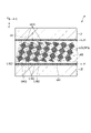
- FIG. 2 is a cross-sectional view showing an example of a liquid crystal element 20 having a reflective polarization grating RPG.
- the liquid crystal element 20 includes a transparent substrate (second transparent substrate) 21, an alignment film AL21, a liquid crystal layer (second liquid crystal layer) LC2, an alignment film AL22, and a transparent substrate 22.
- the transparent substrate 21 faces the transparent substrate 22 in the third direction Z.
- the liquid crystal layer LC2 functions as a polarization diffraction grating RPG and is positioned between the transparent substrates 21 and 22 .
- the transparent substrates 21 and 22 are composed of, for example, transparent glass plates or transparent synthetic resin plates.
- the transparent substrate 21 has an inner surface 21A.
- the transparent substrate 22 has an inner surface 22A.
- the inner surfaces 21A and 22A are surfaces parallel to the XY plane.
- the alignment film AL21 is arranged on the inner surface 21A of the transparent substrate 21.
- the alignment film AL22 is arranged on the inner surface 22A of the transparent substrate 22 .
- the alignment film AL22 faces the alignment film AL21 in the third Z direction.
- the alignment films AL21 and AL22 are horizontal alignment films made of, for example, polyimide and having an alignment control force along the XY plane.
- the alignment films AL21 and AL22 are photo-alignment films for forming a spatially varying liquid crystal alignment pattern.
- the liquid crystal layer LC2 is arranged between the alignment films AL21 and AL22 and is in contact with the alignment films AL21 and AL22.
- the liquid crystal layer LC2 has a main surface LS2.
- the main surface LS2 here is, for example, a boundary between the liquid crystal layer LC2 and the alignment film AL22, and a surface parallel to the XY plane.
- the liquid crystal layer LC2 has a thickness d2 along the third direction Z.
- the liquid crystal layer LC2 has cholesteric liquid crystal.
- one liquid crystal molecule LM2 among a plurality of liquid crystal molecules positioned on the same plane parallel to the XY plane is shown as the liquid crystal molecule LM2 forming the cholesteric liquid crystal.
- the orientation direction of the liquid crystal molecules LM2 corresponds to the average orientation direction of a plurality of liquid crystal molecules positioned on the same plane.
- the liquid crystal layer LC2 has a plurality of liquid crystal structures LMS2. Focusing on one liquid crystal structure LMS2, the liquid crystal structure LMS2 has a liquid crystal molecule LM21 located on one end side and a liquid crystal molecule LM22 located on the other end side. The liquid crystal molecules LM21 are close to the alignment film AL21, and the liquid crystal molecules LM22 are close to the alignment film AL22. A plurality of liquid crystal molecules LM2 including the liquid crystal molecules LM21 and LM22 are spirally stacked around the spiral axis AX to form a cholesteric liquid crystal. That is, the liquid crystal structure LMS2 corresponds to cholesteric liquid crystal.
- the liquid crystal structure LMS2 has a helical pitch P.
- the helical pitch P indicates one helical period (thickness along the helical axis AX required for the liquid crystal molecules LM2 to rotate 360 degrees).
- the thickness d2 of the liquid crystal layer LC2 is several times the helical pitch P or more.
- the helical axis AX of the liquid crystal structure LMS2 is parallel to the third direction Z, which is the normal direction of the liquid crystal layer LC2.
- the plurality of liquid crystal structures LMS2 are aligned in the first direction X and also aligned in the second direction Y.
- a plurality of liquid crystal structures LMS2 adjacent along the first direction X have different alignment directions.
- the alignment direction of the multiple liquid crystal molecules LM21 aligned along the alignment film AL21 and the alignment direction of the multiple liquid crystal molecules LM22 aligned along the alignment film AL22 change continuously.
- the alignment directions of the plurality of liquid crystal structures LMS2 adjacent to each other along the second direction Y are aligned.
- the liquid crystal layer LC2 has a plurality of reflecting surfaces RS indicated by dashed lines between the alignment films AL21 and AL22.
- the multiple reflective surfaces RS are substantially parallel to each other.
- the reflective surface RS reflects a portion of circularly polarized incident light and transmits other circularly polarized light.
- the reflection surface RS corresponds to a surface in which the alignment directions of the liquid crystal molecules LM2 are aligned or a surface in which spatial phases are aligned (equiphase surface).
- the reflective surface RS is inclined with respect to the main surface LS2 of the liquid crystal layer LC2.
- the liquid crystal structure LMS2 reflects circularly polarized light with the same turning direction as that of the cholesteric liquid crystal out of the light of the specific wavelength ⁇ .
- the rotation direction of the cholesteric liquid crystal is clockwise
- the clockwise circularly polarized light of the light of the specific wavelength ⁇ is reflected, and the counterclockwise circularly polarized light is transmitted.
- the rotation direction of the cholesteric liquid crystal is counterclockwise, the counterclockwise circularly polarized light of the light of the specific wavelength ⁇ is reflected, and the clockwise circularly polarized light is transmitted.
- Such a liquid crystal layer LC2 is cured in a state in which the alignment directions of the liquid crystal molecules LM2 including the liquid crystal molecules LM21 and the liquid crystal molecules LM22 are fixed. In other words, the alignment direction of the liquid crystal molecules LM2 is not controlled according to the electric field. Therefore, the liquid crystal element 20 does not have electrodes for alignment control.
- the selective reflection band ⁇ of the cholesteric liquid crystal for vertically incident light is determined based on the helical pitch P of the cholesteric liquid crystal, the refractive index ne for extraordinary light, and the refractive index no for ordinary light. P”. Therefore, in order to efficiently reflect the circularly polarized light of the specific wavelength ⁇ on the reflecting surface RS, the helical pitch P and the refractive indices ne and no are set so that the specific wavelength ⁇ is included in the selective reflection wavelength band ⁇ . .
- the liquid crystal layer LC2 functioning as the polarization diffraction grating RPG is positioned between the pair of transparent substrates 21 and 22, but at least one of the transparent substrates 21 and 22 may be omitted, At least one of the alignment films AL21 and AL22 may be omitted. Also, a plurality of polarization diffraction gratings RPG may be stacked along the third direction Z. FIG.
- FIG. 3 is a cross-sectional view showing a modification of the liquid crystal element 20. As shown in FIG. 3 is different from the example shown in FIG. 2 in that the helical axis AX of the liquid crystal structure LMS2 is inclined with respect to the normal direction (third direction Z) of the liquid crystal layer LC2. are different.
- the multiple liquid crystal structures LMS2 adjacent along the first direction X have different alignment directions.
- the alignment direction of the multiple liquid crystal molecules LM21 aligned along the alignment film AL21 and the alignment direction of the multiple liquid crystal molecules LM22 aligned along the alignment film AL22 change continuously.
- the liquid crystal layer LC2 has a plurality of reflecting surfaces RS indicated by dashed lines between the alignment films AL21 and AL22.
- the multiple reflective surfaces RS are substantially parallel to each other. According to Bragg's law, the reflective surface RS reflects a portion of circularly polarized incident light and transmits other circularly polarized light. In the XZ cross section shown in FIG. 3, the reflective surface RS is inclined with respect to the main surface LS2 of the liquid crystal layer LC2.
- FIG. 4 is a diagram for explaining the optical action of the transmission-type polarization diffraction grating TPG.
- the polarization grating TPG is divided into the first circularly polarized light C1 and the second circularly polarized light C1 of the light NP.
- the two circularly polarized light beams C2 are respectively diffracted.
- the second circularly polarized light C2 is circularly polarized light having a rotation opposite to that of the first circularly polarized light C1.
- the second circularly polarized light C2 is diffracted in a direction different from that of the first circularly polarized light C1.
- the first circularly polarized light C1 is diffracted diagonally to the right from the polarization grating TPG
- the second circularly polarized light C2 is diffracted diagonally to the left from the polarization grating TPG. That is, when the unpolarized light NP is the incident light, the polarization grating TPG separates the light NP into the first circularly polarized light C1 and the second circularly polarized light C2.
- the polarization diffraction grating TPG converts the first circularly polarized light C1 into the second circularly polarized light C2. Transform and diffract.
- the first circularly polarized light C1 incident obliquely to the right toward the polarization grating TPG is converted into the second circularly polarized light C2 and diffracted in the normal direction of the polarization grating TPG.
- the polarization grating TPG converts the second circularly polarized light C2 into the first circularly polarized light C1. Transform and diffract.
- the second circularly polarized light C2 incident obliquely to the left toward the polarization grating TPG is converted into the first circularly polarized light C1 and diffracted in the normal direction of the polarization grating TPG. That is, when the incident light is circularly polarized light, the polarization diffraction grating TPG diffracts the transmitted light while converting it into reverse circularly polarized light.
- FIG. 5 is a diagram for explaining the optical action of the reflective polarization diffraction grating RPG.
- the polarization grating RPG reflects the first circularly polarized light C1 of the light NP.
- the second circularly polarized light C2 is transmitted while being reflected by the surface RS.
- the first circularly polarized light C1 is obliquely reflected at the inclined reflecting surface RS.
- the second circularly polarized light C2 passes through the reflecting surface RS and travels straight in the normal direction of the polarization diffraction grating RPG.
- the polarization diffraction grating RPG As shown on the right side of FIG. 5, when unpolarized light NP as incident light is incident on the polarization diffraction grating RPG from an oblique direction, the polarization diffraction grating RPG The polarized light C1 is reflected by the reflecting surface RS, and the second circularly polarized light C2 is transmitted. The first circularly polarized light C1 is reflected in the normal direction at the inclined reflective surface RS. The second circularly polarized light C2 passes through the reflecting surface RS and travels straight in an oblique direction with respect to the polarization diffraction grating RPG.
- the polarization conversion element 1 Several configuration examples of the polarization conversion element 1 will be described below.
- the first circularly polarized light and the second circularly polarized light separated by the transmissive polarization grating TPG are denoted by C10 and C20, respectively, and the circularly polarized lights on the optical path of the first circularly polarized light C10 are denoted by C11 and C12. , C13 .
- the circularly polarized light described here may be strictly circularly polarized light, or may be circularly polarized light approximating elliptically polarized light.
- FIG. 6 is a cross-sectional view showing a configuration example of the polarization conversion element 1.
- the polarization conversion element 1 includes a light guide plate (first light guide plate) 3 and a transmissive polarization diffraction grating (first polarization diffraction grating) TPG.
- the light guide plate 3 has a first main surface 3A, a second main surface 3B opposite to the first main surface 3A, and side surfaces 3C.
- the light guide plate 3 is made of, for example, a transparent glass plate or a transparent synthetic resin plate.
- the side surface 3C is a surface formed along the thickness direction of the light guide plate 3 .
- the polarization diffraction grating TPG faces the side surface 3C.
- the polarization diffraction grating TPG here corresponds to the liquid crystal layer LC1 in the liquid crystal element 10 shown in FIG.
- the liquid crystal element 10 shown in FIG. 1 may face the side surface 3C, and in this case, the transparent substrate 11 is adhered to the side surface 3C.
- the transparent substrate 12 and the alignment film AL12 of the liquid crystal element 10 shown in FIG. 1 may be omitted, and the main surface LS1 of the liquid crystal layer LC1 may be adhered to the side surface 3C.
- the liquid crystal layer LC1 is arranged between the light guide plate 3 and the transparent substrate 11.
- a normal line 3CN of the side surface 3C coincides with the third direction Z shown in FIG. That is, the polarization grating TPG has nematic liquid crystals oriented along the normal 3CN of the side surface 3C.
- a plurality of liquid crystal molecules LM1 forming the liquid crystal structure LMS1 shown in FIG. 1 are aligned along the normal 3CN, and the orientation directions of these liquid crystal molecules LM1 are uniform along the normal 3CN. , as described above, may be slightly twisted.
- the first main surface 3A of the light guide plate 3 is in contact with a low refractive index medium having a lower refractive index than the light guide plate 3.
- the low refractive index medium is, for example, the thin film 4, but may also be air.
- the thin film 4 may be a reflective layer made of a highly reflective material. As will be described later, such a first main surface 3A forms an interface that totally reflects light diffracted by the polarization diffraction grating TPG.
- the light source 5 faces the polarization diffraction grating TPG.
- An optical system including various lenses may be arranged between the light source 5 and the polarization diffraction grating TPG.
- the light source 5 is configured to emit unpolarized light NP toward the polarization grating TPG.
- the light NP emitted from the light source 5 is separated into a first circularly polarized light C10 and a second circularly polarized light C20 at the polarization diffraction grating TPG.
- the first circularly polarized light C10 is right-handed circularly polarized light (R)
- the second circularly polarized light C20 is left-handed circularly polarized light (L).
- the second circularly polarized light C20 is diffracted toward the second main surface 3B of the light guide plate 3 at the polarization diffraction grating TPG.
- the first circularly polarized light C10 is diffracted toward the first main surface 3A of the light guide plate 3 at the polarization diffraction grating TPG.
- the first circularly polarized light C10 that has reached the first main surface 3A at an incident angle equal to or greater than the critical angle is totally reflected at the interface between the light guide plate 3 and the thin film 4 .
- the s-polarized component and the p-polarized component included in the first circularly polarized light C10 are each phase-shifted.
- the totally reflected light C11 is converted into circularly polarized light having a direction opposite to that of the first circularly polarized light C10. That is, the light C11 is counterclockwise circularly polarized light, like the second circularly polarized light C20.
- Such second circularly polarized light C20 and light C11 can be transmitted through the second main surface 3B and can form illumination light with substantially uniform polarization states.
- the polarization conversion element 1 described here it is possible to convert the non-polarized light NP emitted from the light source 5 into light (circularly polarized light) with almost the same polarization state with almost no loss. It is possible to improve the light utilization efficiency.
- a display panel (for example, a liquid crystal panel) PNL which is an example of an illumination target, is arranged so as to overlap the second main surface 3B, as indicated by the dotted line, and is illuminated by illumination light transmitted through the second main surface 3B.
- the polarization conversion element 1, together with the light source 5, can constitute an illumination device IL.
- the polarization conversion element 1, the light source 5, and the display panel PNL can constitute a display device DSP.
- FIG. 7 is a cross-sectional view showing another configuration example of the polarization conversion element 1.
- the polarization conversion element 1 is different from the example shown in FIG. grating) TPG2 and a retardation plate RT.
- the polarization diffraction grating TPG1 facing the side surface 3C is the same as the polarization diffraction grating TPG shown in FIG. 6, and the description thereof is omitted.
- the polarization diffraction grating TPG2 faces the second main surface 3B.
- the polarization diffraction grating TPG2 here corresponds to the liquid crystal layer LC1 of the liquid crystal element 10 shown in FIG.
- the liquid crystal element 10 shown in FIG. 1 may face the second main surface 3B, and in this case, the transparent substrate 11 is adhered to the second main surface 3B.
- the transparent substrate 12 and the alignment film AL12 of the liquid crystal element 10 shown in FIG. 1 may be omitted, and the main surface LS1 of the liquid crystal layer LC1 may be adhered to the second main surface 3B.
- the liquid crystal layer LC1 is arranged between the light guide plate 3 and the transparent substrate 11.
- the normal 3BN of the second main surface 3B matches the third direction Z shown in FIG. That is, the polarization diffraction grating TPG2 has nematic liquid crystal aligned along the normal 3BN of the second main surface 3B.
- a plurality of liquid crystal molecules LM1 forming the liquid crystal structure LMS1 shown in FIG. 1 are aligned along the normal 3BN, and the alignment direction of these liquid crystal molecules LM1 is uniform along the normal 3BN. , as described above, may be slightly twisted.
- the polarization diffraction grating TPG2 may be configured to have a converging or diverging lens action by adjusting the phase distribution according to the alignment state of the liquid crystal molecules.
- the retardation plate RT faces the polarization diffraction grating TPG2.
- the retardation plate RT may be adhered to the polarization diffraction grating TPG2, or an air layer may be interposed between the retardation plate RT and the polarization diffraction grating TPG2.
- the retardation plate RT is a 1/4 wavelength plate, and gives a phase difference of 1/4 wavelength to the transmitted light.
- the retardation plate RT gives, for example, a phase difference of 1/4 wavelength to light of a specific wavelength, but it is not limited to this.
- the retardation plate RT it is possible to apply a broadband retardation plate that imparts a phase difference of approximately 1/4 wavelength to light of each wavelength in the visible light range.
- the light NP emitted from the light source 5 is separated into a first circularly polarized light C10 and a second circularly polarized light C20 at the polarization diffraction grating TPG1.
- the first circularly polarized light C10 is right-handed circularly polarized light (R)
- the second circularly polarized light C20 is left-handed circularly polarized light (L).
- the first circularly polarized light C10 is diffracted toward the first main surface 3A of the light guide plate 3 at the polarization diffraction grating TPG1.
- the light C11 totally reflected by the first main surface 3A is converted into circularly polarized light having a direction opposite to that of the first circularly polarized light C10. That is, the light C11 is counterclockwise circularly polarized light.
- the light C11 is diffracted in the direction along the normal 3BN at the polarization diffraction grating TPG2, and converted into circularly polarized light having a direction opposite to that of the light C11. That is, the light C12 diffracted by the polarization diffraction grating TPG2 is clockwise circularly polarized light.
- Light C12 is converted into light C13, which is linearly polarized light (PL), at the retardation plate RT.
- the second circularly polarized light C20 is diffracted toward the second main surface 3B of the light guide plate 3 at the polarization diffraction grating TPG1.
- the second circularly polarized light C20 is diffracted in the direction along the normal 3BN at the polarization diffraction grating TPG2, and converted into circularly polarized light having a direction opposite to that of the second circularly polarized light C20. That is, the light C21 diffracted by the polarization diffraction grating TPG2 is clockwise circularly polarized light.
- Light C21 is converted into light C22, which is linearly polarized light (PL), at the retardation plate RT.
- Such light C12 and light C22 can form linearly polarized illumination light with generally aligned polarization axes.
- the display panel PNL which is an example of an illumination target, is arranged so as to overlap the retardation plate RT, and is illuminated by illumination light transmitted through the retardation plate RT.
- a polarization conversion element 1 it is possible to convert the non-polarized light NP emitted from the light source 5 into light (linearly polarized light) having a generally uniform polarization state, thereby improving the light utilization efficiency. be able to.
- FIG. 8 is a cross-sectional view showing another configuration example of the polarization conversion element 1.
- the polarization conversion element 1 in comparison with the example shown in FIG. 6, in addition to the light guide plate 3 and the transmissive polarization diffraction grating TPG, the polarization conversion element 1 includes a reflection polarization diffraction grating RPG and a retardation plate. RT and are different in that they are provided.
- the polarization diffraction grating TPG faces the side surface 3C.
- the polarization diffraction grating TPG here corresponds to the liquid crystal layer LC1 in the liquid crystal element 10 shown in FIG.
- the liquid crystal element 10 shown in FIG. 1 may face the side surface 3C, and in this case, the transparent substrate 11 is adhered to the side surface 3C.
- the transparent substrate 12 and the alignment film AL12 of the liquid crystal element 10 shown in FIG. 1 may be omitted, and the main surface LS1 of the liquid crystal layer LC1 may be adhered to the side surface 3C.
- the liquid crystal layer LC1 is arranged between the light guide plate 3 and the transparent substrate 11.
- a normal line 3CN of the side surface 3C coincides with the third direction Z shown in FIG. That is, the polarization grating TPG has nematic liquid crystals oriented along the normal 3CN of the side surface 3C.
- a plurality of liquid crystal molecules LM1 forming the liquid crystal structure LMS1 shown in FIG. 1 are aligned along the normal 3CN, and the orientation directions of these liquid crystal molecules LM1 are uniform along the normal 3CN. , as described above, may be slightly twisted.
- the polarization diffraction grating RPG faces the first main surface 3A.
- the polarization diffraction grating RPG here corresponds to, for example, the liquid crystal layer LC2 of the liquid crystal element 20 shown in FIG.
- the liquid crystal element 20 shown in FIG. 2 may face the first main surface 3A, and in this case, the transparent substrate 21 is adhered to the first main surface 3A.
- the transparent substrate 22 and the alignment film AL22 of the liquid crystal element 20 shown in FIG. 2 may be omitted, and the main surface LS2 of the liquid crystal layer LC2 may be adhered to the first main surface 3A.
- the liquid crystal layer LC2 is arranged between the light guide plate 3 and the transparent substrate 21.
- the normal 3AN of the first main surface 3A coincides with the third direction Z shown in FIG. That is, the polarization diffraction grating RPG has cholesteric liquid crystals CL, and the spiral axis AX of the cholesteric liquid crystals CL is substantially parallel to the normal line 3AN of the first main surface 3A.
- the polarization grating RPG is the liquid crystal layer LC2 of the liquid crystal element 20 shown in FIG. 3
- the helical axis AX of the cholesteric liquid crystal CL is inclined with respect to the normal 3AN.
- the polarization diffraction grating RPG has a reflecting surface RS inclined with respect to the first main surface 3A.
- the cholesteric liquid crystal CL is schematically shown on the right side of the figure.
- the cholesteric liquid crystal CL is spiraled to reflect right-handed circularly polarized light of a particular wavelength ⁇ and has a helical pitch P along the helical axis AX.
- the helical pitch P is constant with little change along the helical axis AX.
- the retardation plate RT faces the second main surface 3B.
- the retardation plate RT may be adhered to the light guide plate 3 , or an air layer may be interposed between the retardation plate RT and the light guide plate 3 .
- the retardation plate RT is a 1/4 wavelength plate, and gives a phase difference of 1/4 wavelength to the transmitted light.
- the non-polarized light NP emitted from the light source 5 is separated into a first circularly polarized light C10 and a second circularly polarized light C20 at the polarization diffraction grating TPG.
- the first circularly polarized light C10 is right-handed circularly polarized light (R)
- the second circularly polarized light C20 is left-handed circularly polarized light (L).
- the first circularly polarized light C10 is diffracted toward the first main surface 3A of the light guide plate 3 at the polarization diffraction grating TPG.
- the diffracted first circularly polarized light C10 is transmitted through the first main surface 3A and reflected in the direction along the normal 3AN on the reflecting surface RS of the polarization diffraction grating RPG.
- the reflected light C11 is a clockwise circularly polarized light similar to the first circularly polarized light C10.
- the light C11 is transmitted through the second principal surface 3B and converted into the light C12, which is linearly polarized light (PL), by the retardation plate RT.
- the second circularly polarized light C20 is diffracted toward the second main surface 3B of the light guide plate 3 at the polarization diffraction grating TPG.
- the second circularly polarized light C20 that has reached the second main surface 3B at an incident angle equal to or greater than the critical angle is totally reflected at the interface between the light guide plate 3 and the retardation plate RT.
- the totally reflected light C21 is converted into circularly polarized light having a direction opposite to that of the second circularly polarized light C20. That is, the light C21 is clockwise circularly polarized light.
- the light C21 is transmitted through the first main surface 3A and reflected in the direction along the normal 3AN on the reflecting surface RS of the polarization diffraction grating RPG.
- the reflected light C22 is right-handed circularly polarized light, similar to light C21.
- the light C22 is transmitted through the second main surface 3B and converted into light C23, which is linearly polarized light (PL
- Such light C12 and light C23 can form linearly polarized illumination light with generally aligned polarization axes.
- the display panel PNL which is an example of an illumination target, is arranged so as to overlap the retardation plate RT, and is illuminated by illumination light transmitted through the retardation plate RT.
- a polarization conversion element 1 it is possible to convert the non-polarized light NP emitted from the light source 5 into light (linearly polarized light) having a generally uniform polarization state, thereby improving the light utilization efficiency. be able to.
- a light diffusion sheet, a prism sheet, a polarizer, or the like may be arranged between the retardation plate RT and the display panel PNL.
- FIG. 9 is a cross-sectional view showing another configuration example of the polarization conversion element 1. As shown in FIG. The example shown in FIG. 9 differs from the example shown in FIG. 8 in that the polarization grating RPG has a thickness distribution.
- the polarization diffraction grating RPG has multiple areas A1 to A4.
- the area A1 first area is located on the side close to the polarization diffraction grating TPG or the light source 5 .
- the area A2 second area is positioned away from the polarization grating TPG, and the area A1 is positioned between the polarization grating TPG and the area A2.
- Area A2 is located between area A1 and area A3, and area A3 is located between area A2 and area A4. That is, the areas A1 to A4 are arranged in order toward the side away from the polarization diffraction grating TPG. The thickness relationships of these regions A1 to A4 will be described below.
- FIG. 10 is a diagram for explaining the regions A1 to 4A of the polarization diffraction grating RPG.
- a region A1 is a region having cholesteric liquid crystal CL1 and has a thickness T1.
- a region A2 is a region having cholesteric liquid crystal CL2 and has a thickness T2.
- a region A3 is a region having cholesteric liquid crystal CL3 and has a thickness T3.
- a region A4 is a region having cholesteric liquid crystal CL4 and has a thickness T4.
- the thickness here is, for example, the length along the normal 3AN of the first main surface 3A with which the polarization diffraction grating RPG is in contact.
- the thickness T1 of the region A1 is smaller than the thickness T2 of the region A2, the thickness T2 of the region A2 is smaller than the thickness T3 of the region A3, and the thickness T3 of the region A3 is smaller than the thickness T4 of the region A4 (T1 ⁇ T2 ⁇ T3 ⁇ T4).
- Each of the cholesteric liquid crystals CL1 to CL4 has the same helical pitch P.
- the length L1 along the helical axis AX of the cholesteric liquid crystal CL1 is substantially equal to the thickness T1 and is denoted as P*N1.
- the length L2 of the cholesteric liquid crystal CL2 is substantially equal to the thickness T2 and is denoted as P*N2.
- the length L3 of the cholesteric liquid crystal CL3 is substantially equal to the thickness T3 and is denoted as P*N3.
- the length L4 of the cholesteric liquid crystal CL4 is substantially equal to the thickness T4 and is denoted as P*N4.
- N1 to N4 are 10 or less, for example.
- N1 is smaller than N2, N2 is smaller than N3, and N3 is smaller than N4 (N1 ⁇ N2 ⁇ N3 ⁇ N4).
- the length L1 is smaller than the length L2, the length L2 is smaller than the length L3, and the length L3 is smaller than the length L4 (L1 ⁇ L2 ⁇ L3 ⁇ L4).
- the coefficients (N1 to N4) are in the range of, for example, 10 or less, the larger the coefficient, the higher the reflectance tends to be. Therefore, the reflectance of the cholesteric liquid crystal CL2 in the area A2 is higher than the reflectance of the cholesteric liquid crystal CL1 in the area A1. Similarly, the reflectance of area A3 is higher than that of area A2, and the reflectance of area A4 is higher than that of area A3.
- the non-polarized light NP emitted from the light source 5 is separated into a first circularly polarized light C10 and a second circularly polarized light C20 at the polarization diffraction grating TPG.
- the first circularly polarized light C10 is right-handed circularly polarized light (R)
- the second circularly polarized light C20 is left-handed circularly polarized light (L).
- the first circularly polarized light C10 is diffracted toward the first main surface 3A of the light guide plate 3 at the polarization diffraction grating TPG. Part of the diffracted first circularly polarized light C10 is reflected in the direction along the normal 3AN on the reflecting surface RS formed in the area A1 of the polarization diffraction grating RPG.
- the reflected light C11 is right-handed circularly polarized light similar to the first circularly polarized light C10, and is converted into linearly polarized light (PL) at the retardation plate RT.
- the diffracted first circularly polarized light C10 are totally reflected and converted into circularly polarized light having a direction opposite to that of the first circularly polarized light C10. That is, the totally reflected light C12 is counterclockwise circularly polarized light.
- the light C12 is totally reflected by the second main surface 3B and converted into circularly polarized light having a direction opposite to that of the light C12. That is, the totally reflected light C13 is clockwise circularly polarized light.
- Part of the light C13 is reflected in a direction along the normal line 3AN at the reflecting surface RS formed in the area A3 of the polarization grating RPG.
- the reflected light C14 is right-handed circularly polarized light and is converted into linearly polarized light (PL) at the retardation plate RT.
- the second circularly polarized light C20 is diffracted toward the second main surface 3B of the light guide plate 3 at the polarization diffraction grating TPG.
- the diffracted second circularly polarized light C20 is totally reflected by the second main surface 3B and converted into circularly polarized light having a direction opposite to that of the second circularly polarized light C20. That is, the totally reflected light C21 is clockwise circularly polarized light.
- Part of the light C21 is reflected in a direction along the normal 3AN on the reflecting surface RS formed in the area A2 of the polarization diffraction grating RPG.
- the reflected light C22 is right-handed circularly polarized light and is converted into linearly polarized light (PL) at the retardation plate RT.
- the light C21 are totally reflected and converted into circularly polarized light having a direction opposite to that of the light C21. That is, the totally reflected light C23 is converted into counterclockwise circularly polarized light.
- the light C23 is totally reflected by the second main surface 3B and converted into circularly polarized light having a direction opposite to that of the light C23. That is, the totally reflected light C24 is clockwise circularly polarized light.
- Part of the light C24 is reflected in the direction along the normal 3AN at the reflecting surface RS formed in the area A4 of the polarization grating RPG.
- the reflected light C25 is right-handed circularly polarized light and is converted into linearly polarized light (PL) at the retardation plate RT.
- FIG. 11 is a cross-sectional view showing another example of the liquid crystal element 20 provided with the polarization diffraction grating RPG.
- a liquid crystal layer LC2 corresponding to the polarization diffraction grating RPG has a plurality of liquid crystal structures (cholesteric liquid crystals) LMS2.
- a plurality of liquid crystal molecules LM2 forming the liquid crystal structure LMS2 are cured with their alignment directions fixed.
- the liquid crystal layer LC2 has a plurality of reflecting surfaces RS indicated by dotted lines between the alignment films AL21 and AL22.
- the reflecting surface RS is a curved surface, concave on the side facing the transparent substrate 22 and convex on the side facing the transparent substrate 21 .
- the reflecting surface RS may be convex toward the side facing the transparent substrate 22 .
- Such a liquid crystal element 20 has a lens action of reflecting a part of the circularly polarized light of the incident light and converging or diverging it on the reflecting surface RS.
- FIG. 12 is a cross-sectional view showing another configuration example of the polarization conversion element 1.
- the polarization conversion element 1 includes the polarization diffraction grating RPG shown in FIG. Description of each part is omitted.
- the light on each optical path is given the same reference numerals as in the example shown in FIG. 9, and detailed description thereof is omitted.
- a part of the first circularly polarized light C10 is reflected by the reflecting surface RS of the polarization diffraction grating RPG and diverges under the lens action of the polarization diffraction grating RPG.
- a portion of the light C13, a portion of the light C21, and a portion of the light C24, which are circularly polarized light similar to the first circularly polarized light C10, are each reflected on the reflecting surface RS and diverged.
- the shape of the reflecting surface RS it is possible to reflect and converge circularly polarized light similar to the first circularly polarized light C10.
- FIG. 13 is a cross-sectional view showing another configuration example of the polarization conversion element 1.
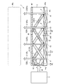
- the polarization conversion element 1 includes a plurality of reflective polarization gratings RPG1 in addition to the transmission type polarization grating (first polarization grating) TPG. , RPG2, and RPG3.
- the polarization grating (second polarization grating) RPG1 has a reflecting surface RS1
- the polarization grating (third polarization grating) RPG2 has a reflecting surface RS2
- the polarization grating RPG3 has a reflecting surface RS3.
- the inclination angles ⁇ 1 to ⁇ 3 of each of the reflecting surfaces RS1 to RS3 with respect to the plane parallel to the first main surface 3A are substantially the same.
- the polarization diffraction grating RPG2 faces the polarization diffraction grating RPG1 and is arranged between the polarization diffraction grating RPG1 and the light guide plate 3.
- the polarization diffraction grating RPG3 faces the polarization diffraction grating RPG2 and is arranged between the polarization diffraction grating RPG2 and the light guide plate 3 .
- Polarization diffraction grating RPG3 is in contact with first main surface 3A.
- the polarization diffraction grating RPG1, the polarization diffraction grating RPG2, and the polarization diffraction grating RPG3 are laminated along the normal line 3AN. Note that the stacking order of the polarization diffraction grating RPG1, the polarization diffraction grating RPG2, and the polarization diffraction grating RPG3 is not limited to the illustrated example.
- the polarization diffraction grating RPG1, the polarization diffraction grating RPG2, and the polarization diffraction grating RPG3 are equivalent to the liquid crystal element 20 described with reference to FIGS.
- the helical pitches of the polarization diffraction grating RPG1, the polarization diffraction grating RPG2, and the polarization diffraction grating RPG3 are different from each other. This point will be described below.
- FIG. 14 is a diagram schematically showing the polarization diffraction gratings RPG1 to RPG3.
- Polarization grating RPG1 is configured to reflect the first circularly polarized light at the red wavelength.
- Cholesteric liquid crystal CL1 included in polarization grating RPG1 has a helical pitch P1 along helical axis AX1.
- the helical pitch P1 is optimized to correspond to red wavelengths.
- Such cholesteric liquid crystal CL1 forms the reflecting surface RS1 shown in FIG.
- the polarization grating RPG2 is configured to reflect the first circularly polarized light of the green wavelength. That is, the turning direction of the cholesteric liquid crystal CL2 included in the polarization diffraction grating RPG2 is the same as the turning direction of the cholesteric liquid crystal CL1. Further, the helical axis AX2 of the cholesteric liquid crystal CL2 is substantially parallel to the helical axis AX1 of the cholesteric liquid crystal CL1.
- the cholesteric liquid crystal CL2 has a helical pitch P2 along the helical axis AX2. The helical pitch P2 is smaller than the helical pitch P1 (P2 ⁇ P1). The helical pitch P2 is optimized to correspond to the green wavelength.
- Such cholesteric liquid crystal CL2 forms the reflecting surface RS2 shown in FIG.
- the polarization grating RPG3 is configured to reflect the first circularly polarized light of blue wavelength. That is, the turning direction of the cholesteric liquid crystal CL3 included in the polarization diffraction grating RPG3 is the same as the turning direction of the cholesteric liquid crystal CL2. Further, the helical axis AX3 of the cholesteric liquid crystal CL3 is substantially parallel to the helical axis AX2 of the cholesteric liquid crystal CL2.
- the cholesteric liquid crystal CL3 has a helical pitch P3 along the helical axis AX3. The helical pitch P3 is smaller than the helical pitch P2 (P3 ⁇ P2). The helical pitch P3 is optimized for blue wavelengths.
- Such cholesteric liquid crystal CL3 forms the reflecting surface RS3 shown in FIG.
- the light source 5 emits unpolarized light NP toward the polarization grating TPG.
- the light NP includes components of red wavelength ( ⁇ R), green wavelength ( ⁇ G), and blue wavelength ( ⁇ B).
- the light NP is separated into the first circularly polarized light C10 and the second circularly polarized light C20 at the polarization diffraction grating TPG, but only the first circularly polarized light C10 diffracted toward the first principal surface 3A is shown here.
- the first circularly polarized light C10 is, for example, clockwise circularly polarized light.
- the longer the wavelength the larger the diffraction angle with respect to the normal 3CN of the first circularly polarized light C10 diffracted by the polarization diffraction grating TPG. Therefore, the first circularly polarized light RC10 of the red wavelength is diffracted at a larger diffraction angle than the first circularly polarized light GC10 of the green wavelength. Also, the green wavelength first circularly polarized light GC10 is diffracted at a larger diffraction angle than the blue wavelength first circularly polarized light BC10.
- the first circularly polarized light RC10 passes through the polarization gratings RPG3 and RPG2 and is reflected by the reflecting surface RS1 of the polarization grating RPG1.
- the first circularly polarized light GC10 passes through the polarization grating RPG3 and is reflected by the reflecting surface RS2 of the polarization grating RPG2.
- the first circularly polarized light BC10 is reflected at the reflecting surface RS3 of the polarization grating RPG3.
- the inclination angles ⁇ 1 to ⁇ 3 of the reflecting surfaces RS1 to RS3 are substantially the same, the light RC11 reflected by the reflecting surface RS1, the light GC11 reflected by the reflecting surface RS2, and the reflecting surface RS3
- the reflected light BC11 is transmitted through the second main surface 3B at different angles with respect to the normal 3BN of the second main surface 3B.
- Light RC11, light GC11, and light BC11 are clockwise circularly polarized light similar to the first circularly polarized light, and are converted into linearly polarized light (PL) by the retardation plate RT.
- FIG. 15 is a cross-sectional view showing another configuration example of the polarization conversion element 1. As shown in FIG. The example shown in FIG. 15 differs from the example shown in FIG. 13 in that the inclination angles ⁇ 1 to ⁇ 3 of the reflecting surfaces RS1 to RS3 are different from each other.
- the tilt angle ⁇ 1 of the reflecting surface RS1 is smaller than the tilt angle ⁇ 2 of the reflecting surface RS2 ( ⁇ 1 ⁇ 2).
- the tilt angle ⁇ 2 of the reflecting surface RS2 is smaller than the tilt angle ⁇ 3 of the reflecting surface RS3 ( ⁇ 2 ⁇ 3).
- the cholesteric liquid crystal CL1 included in the polarization diffraction grating RPG1, the cholesteric liquid crystal CL2 included in the polarization diffraction grating RPG2, and the cholesteric liquid crystal CL3 included in the polarization diffraction grating RPG3 are as described with reference to FIG. .
- the unpolarized light NP emitted from the light source 5 is separated into the first circularly polarized light C10 and the second circularly polarized light C20 at the polarization diffraction grating TPG, and is diffracted here toward the first main surface 3A. Only the first circular polarization C10 is shown.
- the first circularly polarized light C10 is, for example, clockwise circularly polarized light.
- the red wavelength first circularly polarized light RC10 is reflected at the reflecting surface RS1 of the polarization grating RPG1.
- the green wavelength first circularly polarized light GC10 is reflected at the reflective surface RS2 of the polarization grating RPG2.
- the blue wavelength first circularly polarized light BC10 is reflected at the reflective surface RS3 of the polarization grating RPG3.
- the inclination angles ⁇ 1 to ⁇ 3 of the reflecting surfaces RS1 to RS3 make the light RC11 reflected by the reflecting surface RS1, the light GC11 reflected by the reflecting surface RS2, and the light BC11 reflected by the reflecting surface RS3 substantially the same. It is set to reflect in the direction. That is, each of the light RC11, the light GC11, and the light BC11 is transmitted through the second main surface 3B at substantially the same angle with respect to the normal 3BN of the second main surface 3B.
- Light RC11, light GC11, and light BC11 are clockwise circularly polarized light similar to the first circularly polarized light, and are converted into linearly polarized light (PL) by the retardation plate RT.
- chromatic aberration can be reduced compared to the example shown in FIG. Therefore, it is possible to form illumination light with little color unevenness.
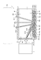
- FIG. 16 is a cross-sectional view showing another configuration example of the polarization conversion element 1.
- the polarization conversion element 1 includes light guide plates 31 to 33, transmission-type polarization diffraction gratings TPG1 to TPG3, reflection-type polarization diffraction gratings RPG1 to RPG3, and a retardation plate RT.
- the polarization diffraction grating RPG1 has a reflecting surface RS1 facing the first main surface 31A of the light guide plate 31 and inclined at an inclination angle ⁇ 1 with respect to the first main surface 31A.
- the polarization diffraction grating RPG2 has a reflecting surface RS2 facing the second main surface 31B of the light guide plate 31 and the first main surface 32A of the light guide plate 32 and inclined at an inclination angle ⁇ 2 with respect to the first main surface 32A.
- the polarization diffraction grating RPG3 has a reflecting surface RS3 facing the second main surface 32B of the light guide plate 32 and the first main surface 33A of the light guide plate 33 and inclined at an inclination angle ⁇ 3 with respect to the first main surface 33A. there is These tilt angles ⁇ 1 to ⁇ 3 are different from each other and are set as described with reference to FIG.
- the polarization diffraction grating TPG1 faces the side surface 31C of the light guide plate 31
- the polarization diffraction grating TPG2 faces the side surface 32C of the light guide plate 32
- the polarization diffraction grating TPG3 faces the side surface 33C of the light guide plate 33.
- a common polarization diffraction grating TPG may be arranged on the side surface 31C, the side surface 32C, and the side surface 33C.
- the polarization diffraction gratings TPG1 to TPG3 separate the unpolarized light into the first circularly polarized light and the second circularly polarized light, respectively, but only the first circularly polarized light is illustrated and the description of the second circularly polarized light is omitted.
- the light source 51 faces the polarization diffraction grating TPG1 and is configured to emit unpolarized light NP1 of red wavelength ( ⁇ R) toward the polarization diffraction grating TPG1.
- the light source 52 faces the polarization diffraction grating TPG2 and is configured to emit green wavelength ( ⁇ G) unpolarized light NP2 toward the polarization diffraction grating TPG2.
- the light source 53 is configured to face the polarization diffraction grating TPG3 and emit unpolarized light NP3 of blue wavelength ( ⁇ B) toward the polarization diffraction grating TPG3.
- the first circularly polarized light RC10 of the light NP1 is diffracted toward the first main surface 31A by the polarization diffraction grating TPG1.
- the first circularly polarized light RC10 is reflected at the reflective surface RS1 of the polarization grating RPG1.
- the light RC11 reflected by the reflecting surface RS1 passes through the polarization diffraction grating RPG2, the light guide plate 32, the polarization diffraction grating RPG3, and the light guide plate 33, and is converted into linearly polarized light by the retardation plate RT.
- the first circularly polarized light GC10 of the light NP2 is diffracted toward the first main surface 32A by the polarization diffraction grating TPG2.
- the first circularly polarized light GC10 is reflected at the reflecting surface RS2 of the polarization grating RPG2.
- the light GC11 reflected by the reflecting surface RS2 passes through the polarization diffraction grating RPG3 and the light guide plate 33, and is converted into linearly polarized light by the retardation plate RT.
- the first circularly polarized light BC10 of the light NP3 is diffracted toward the first main surface 33A by the polarization diffraction grating TPG3.
- the first circularly polarized light BC10 is reflected at the reflecting surface RS3 of the polarization grating RPG3.
- the light BC11 reflected by the reflecting surface RS3 is converted into linearly polarized light by the retardation plate RT.
Landscapes
- Physics & Mathematics (AREA)
- General Physics & Mathematics (AREA)
- Optics & Photonics (AREA)
- Nonlinear Science (AREA)
- Chemical & Material Sciences (AREA)
- Crystallography & Structural Chemistry (AREA)
- Mathematical Physics (AREA)
- Spectroscopy & Molecular Physics (AREA)
- Polarising Elements (AREA)
- Diffracting Gratings Or Hologram Optical Elements (AREA)
Abstract
The purpose of the present embodiment is to improve light use efficiency. According to an embodiment, a polarization conversion element comprises: a first light-guiding plate having a first principal surface, a second principal surface on the reverse side from the first principal surface, and a side surface; a transmission-type first polarization diffraction grating facing the side surface; and a reflection-type second polarization diffraction grating facing the first principal surface. The first polarization diffraction grating has a nematic liquid crystal oriented along the normal direction of the side surface, and is configured to diffract first circularly polarized light out of incident light in an unpolarized state and diffract second circularly polarized light reverse to the first circularly polarized light in a direction different from that of the first circularly polarized light, and the second polarization diffraction grating has a cholesteric liquid crystal that forms a reflection surface inclined with respect to the first principal surface, and is configured to reflect the first circularly polarized light on the reflection surface.
Description
本発明の実施形態は、偏光変換素子に関する。
Embodiments of the present invention relate to polarization conversion elements.
近年、非偏光状態の光を所定の円偏光あるいは直線偏光に変換する偏光変換素子が開発されている。一例では、所定のパターンで配向した液晶分子を有する液晶素子が透過型の偏光回折格子(Polarization Grating)として適用された偏光変換素子が提案されている。この偏光回折格子は、非偏光状態の光を、右回りの円偏光と左回りの円偏光とに分離するように構成されている。
In recent years, polarization conversion elements have been developed that convert unpolarized light into predetermined circularly polarized light or linearly polarized light. As one example, a polarization conversion element is proposed in which a liquid crystal element having liquid crystal molecules aligned in a predetermined pattern is applied as a transmission type polarization grating. The polarization grating is configured to separate unpolarized light into right-handed circularly polarized light and left-handed circularly polarized light.
実施形態の目的は、光の利用効率を向上することが可能な偏光変換素子を提供することにある。
An object of the embodiments is to provide a polarization conversion element capable of improving light utilization efficiency.
一実施形態によれば、偏光変換素子は、
第1主面と、前記第1主面と反対側の第2主面と、側面と、を有する第1導光板と、前記側面に対向する透過型の第1偏光回折格子と、前記第1主面に対向する反射型の第2偏光回折格子と、を備え、前記第1偏光回折格子は、前記側面の法線方向に沿って配向したネマティック液晶を有し、無偏光状態の入射光のうち第1円偏光を回折するとともに第1円偏光とは逆回りの第2円偏光を前記第1円偏光とは異なる方向に回折するように構成され、前記第2偏光回折格子は、前記第1主面に対して傾斜した反射面を形成するコレステリック液晶を有し、前記反射面において前記第1円偏光を反射するように構成されている。
また、一実施形態によれば、偏光変換素子は、
第1主面と、前記第1主面と反対側の第2主面と、側面と、を有する第1導光板と、前記側面に対向する透過型の第1偏光回折格子と、前記第2主面に対向する透過型の第2偏光回折格子と、を備え、前記第1偏光回折格子は、前記側面の法線方向に沿って配向したネマティック液晶を有し、無偏光状態の入射光のうち第1円偏光を回折するとともに第1円偏光とは逆回りの第2円偏光を前記第1円偏光とは異なる方向に回折するように構成され、前記第2偏光回折格子は、前記第2主面の法線方向に沿って配向したネマティック液晶を有し、前記第1円偏光及び前記第2円偏光を回折するように構成されている。 According to one embodiment, the polarization conversion element comprises
a first light guide plate having a first main surface, a second main surface opposite to the first main surface, and side surfaces; a transmissive first polarization diffraction grating facing the side surfaces; a reflective second polarization diffraction grating facing the main surface, the first polarization diffraction grating having nematic liquid crystals oriented along the normal direction of the side surface, and Among them, it is configured to diffract the first circularly polarized light and diffract the second circularly polarized light opposite to the first circularly polarized light in a direction different from that of the first circularly polarized light, and the second polarization diffraction grating is configured to It has cholesteric liquid crystals forming a reflective surface inclined with respect to one main surface, and is configured to reflect the first circularly polarized light on the reflective surface.
Further, according to one embodiment, the polarization conversion element is
a first light guide plate having a first main surface, a second main surface opposite to the first main surface, and side surfaces; a transmissive first polarization diffraction grating facing the side surfaces; a transmissive second polarizing diffraction grating facing the main surface, wherein the first polarizing diffraction grating has nematic liquid crystals oriented along the normal direction of the side surface, and is configured to transmit unpolarized incident light. Among them, it is configured to diffract the first circularly polarized light and diffract the second circularly polarized light opposite to the first circularly polarized light in a direction different from that of the first circularly polarized light, and the second polarization diffraction grating is configured to It has nematic liquid crystals oriented along the normal directions of the two principal surfaces, and is configured to diffract the first circularly polarized light and the second circularly polarized light.
実施形態によれば、光の利用効率を向上することが可能な偏光変換素子を提供することができる。
According to the embodiment, it is possible to provide a polarization conversion element capable of improving the light utilization efficiency.
以下、本実施形態について、図面を参照しながら説明する。なお、開示はあくまで一例に過ぎず、当業者において、発明の主旨を保っての適宜変更について容易に想到し得るものについては、当然に本発明の範囲に含有されるものである。また、図面は、説明をより明確にするため、実際の態様に比べて、各部の幅、厚さ、形状等について模式的に表される場合があるが、あくまで一例であって、本発明の解釈を限定するものではない。また、本明細書と各図において、既出の図に関して前述したものと同一又は類似した機能を発揮する構成要素には同一の参照符号を付し、重複する詳細な説明を適宜省略することがある。
The present embodiment will be described below with reference to the drawings. It should be noted that the disclosure is merely an example, and those skilled in the art will naturally include within the scope of the present invention any suitable modifications that can be easily conceived while maintaining the gist of the invention. In addition, in order to make the description clearer, the drawings may schematically show the width, thickness, shape, etc. of each part compared to the actual embodiment, but this is only an example and does not apply to the present invention. It does not limit interpretation. In addition, in this specification and each figure, the same reference numerals are given to components that exhibit the same or similar functions as those described above with respect to the previous figures, and redundant detailed description may be omitted as appropriate. .
なお、図面には、必要に応じて理解を容易にするために、互いに直交するX軸、Y軸、及び、Z軸を記載する。X軸に沿った方向をX方向または第1方向と称し、Y軸に沿った方向をY方向または第2方向と称し、Z軸に沿った方向をZ方向または第3方向と称する。X軸及びY軸によって規定される面をX-Y平面と称する。X-Y平面を見ることを平面視という。第1方向X及び第2方向Yは、偏光変換素子に含まれる基板の主面に平行な方向に相当し、また、第3方向Zは、偏光変換素子の厚さ方向に相当する。
In addition, in the drawings, X-axis, Y-axis, and Z-axis, which are orthogonal to each other, are shown as necessary to facilitate understanding. The direction along the X axis is called the X direction or first direction, the direction along the Y axis is called the Y direction or second direction, and the direction along the Z axis is called the Z direction or third direction. A plane defined by the X and Y axes is called the XY plane. Viewing the XY plane is called planar viewing. The first direction X and the second direction Y correspond to directions parallel to the main surface of the substrate included in the polarization conversion element, and the third direction Z corresponds to the thickness direction of the polarization conversion element.
まず、本実施形態の偏光変換素子に適用される偏光回折格子について説明する。
First, the polarization diffraction grating applied to the polarization conversion element of this embodiment will be described.
《透過型偏光回折格子》
図1は、透過型の偏光回折格子TPGを備えた液晶素子10の一例を示す断面図である。
液晶素子10は、透明基板(第1透明基板)11と、配向膜AL11と、液晶層(第1液晶層)LC1と、配向膜AL12と、透明基板12と、を備えている。透明基板11は、第3方向Zにおいて透明基板12と対向している。液晶層LC1は、偏光回折格子TPGとして機能し、透明基板11と透明基板12との間に位置している。 《Transmissive polarization diffraction grating》
FIG. 1 is a cross-sectional view showing an example of aliquid crystal element 10 having a transmissive polarization grating TPG.
Theliquid crystal element 10 includes a transparent substrate (first transparent substrate) 11, an alignment film AL11, a liquid crystal layer (first liquid crystal layer) LC1, an alignment film AL12, and a transparent substrate 12. The transparent substrate 11 faces the transparent substrate 12 in the third direction Z. As shown in FIG. The liquid crystal layer LC1 functions as a polarization diffraction grating TPG and is located between the transparent substrates 11 and 12. As shown in FIG.
図1は、透過型の偏光回折格子TPGを備えた液晶素子10の一例を示す断面図である。
液晶素子10は、透明基板(第1透明基板)11と、配向膜AL11と、液晶層(第1液晶層)LC1と、配向膜AL12と、透明基板12と、を備えている。透明基板11は、第3方向Zにおいて透明基板12と対向している。液晶層LC1は、偏光回折格子TPGとして機能し、透明基板11と透明基板12との間に位置している。 《Transmissive polarization diffraction grating》
FIG. 1 is a cross-sectional view showing an example of a
The
透明基板11及び12は、例えば、透明なガラス板または透明な合成樹脂板によって構成されている。透明基板11は、内面11Aを有している。透明基板12は、内面12Aを有している。内面11A及び12Aは、X-Y平面に平行な面である。
The transparent substrates 11 and 12 are composed of, for example, transparent glass plates or transparent synthetic resin plates. The transparent substrate 11 has an inner surface 11A. The transparent substrate 12 has an inner surface 12A. The inner surfaces 11A and 12A are surfaces parallel to the XY plane.
配向膜AL11は、透明基板11の内面11Aに配置されている。配向膜AL12は、透明基板12の内面12Aに配置されている。配向膜AL12は、第3方向Zにおいて、配向膜AL11と対向している。配向膜AL11及びAL12は、例えば、ポリイミドによって形成され、いずれもX-Y平面に沿った配向規制力を有する水平配向膜である。また、一例では、配向膜AL11及びAL12は、空間的に変化する液晶配向パターンを形成するための光配向膜である。
The alignment film AL11 is arranged on the inner surface 11A of the transparent substrate 11. The alignment film AL12 is arranged on the inner surface 12A of the transparent substrate 12 . The alignment film AL12 faces the alignment film AL11 in the third direction Z. As shown in FIG. The alignment films AL11 and AL12 are horizontal alignment films made of, for example, polyimide and having an alignment control force along the XY plane. In one example, the alignment films AL11 and AL12 are photo-alignment films for forming a spatially varying liquid crystal alignment pattern.
液晶層LC1は、配向膜AL11及びAL12の間に配置され、配向膜AL11及びAL12に接している。液晶層LC1は、主面LS1を有している。ここでの主面LS1は、例えば、液晶層LC1と配向膜AL12との境界であり、また、X-Y平面と平行な面である。液晶層LC1は、第3方向Zに沿った厚さd1を有している。液晶層LC1は、液晶層LC1の法線方向である第3方向Zに沿って配向したネマティック液晶を有している。一例では、ネマティック液晶は、図示したように、第3方向Zにおいて配向方向が揃っている。なお、より広帯域の光に対して同様の光学作用を実現するために、液晶層LC1は、第3方向Zに並んだ液晶分子LM11がわずかにツイストするように配向していてもよい。
The liquid crystal layer LC1 is arranged between the alignment films AL11 and AL12 and is in contact with the alignment films AL11 and AL12. The liquid crystal layer LC1 has a main surface LS1. The main surface LS1 here is, for example, a boundary between the liquid crystal layer LC1 and the alignment film AL12, and a surface parallel to the XY plane. The liquid crystal layer LC1 has a thickness d1 along the third direction Z. The liquid crystal layer LC1 has nematic liquid crystals aligned along the third direction Z, which is the normal direction of the liquid crystal layer LC1. In one example, the nematic liquid crystals are aligned in the third direction Z as shown. In order to achieve the same optical action for light in a wider band, the liquid crystal layer LC1 may be oriented such that the liquid crystal molecules LM11 aligned in the third direction Z are slightly twisted.
すなわち、液晶層LC1は、複数の液晶構造体LMS1を有している。1つの液晶構造体LMS1に着目すると、液晶構造体LMS1は、その一端側に位置する液晶分子LM11と、その他端側に位置する液晶分子LM12と、を有している。液晶分子LM11は配向膜AL11に近接し、液晶分子LM12は配向膜AL12に近接している。液晶分子LM11の配向方向、及び、液晶分子LM12の配向方向は、ほぼ一致している。また、液晶分子LM11と液晶分子LM12との間の他の液晶分子LM1の配向方向も、液晶分子LM11の配向方向とほぼ一致している。つまり、1つの液晶構造体LMS1を構成する液晶分子LM1の配向方向は、第3方向Zにおいて一様である。なお、ここでの液晶分子LM1の配向方向とは、X-Y平面における液晶分子の長軸の方向に相当する。
That is, the liquid crystal layer LC1 has a plurality of liquid crystal structures LMS1. Focusing on one liquid crystal structure LMS1, the liquid crystal structure LMS1 has a liquid crystal molecule LM11 located on one end side and a liquid crystal molecule LM12 located on the other end side. The liquid crystal molecules LM11 are close to the alignment film AL11, and the liquid crystal molecules LM12 are close to the alignment film AL12. The orientation direction of the liquid crystal molecules LM11 and the orientation direction of the liquid crystal molecules LM12 are substantially the same. In addition, the alignment direction of the other liquid crystal molecules LM1 between the liquid crystal molecules LM11 and LM12 also substantially matches the alignment direction of the liquid crystal molecules LM11. That is, the orientation directions of the liquid crystal molecules LM1 forming one liquid crystal structure LMS1 are uniform in the third direction Z. As shown in FIG. The alignment direction of the liquid crystal molecules LM1 here corresponds to the direction of the long axis of the liquid crystal molecules on the XY plane.
液晶層LC1において、複数の液晶構造体LMS1は、第1方向Xに配列されるとともに、第2方向Yにも配列されている。第1方向Xに沿って隣接する複数の液晶構造体LMS1は、互いに配向方向が異なっている。配向膜AL11に近接する複数の液晶分子LM11の配向方向、及び、配向膜AL12に近接する複数の液晶分子LM12の配向方向は、第1方向Xに沿って、液晶分子の長軸が回転するように連続的に変化している。なお、液晶層LC1において、第2方向Yに沿って隣接する複数の液晶構造体LMS1は、互いに配向方向が揃っている。
In the liquid crystal layer LC1, the plurality of liquid crystal structures LMS1 are aligned in the first direction X and also aligned in the second direction Y. A plurality of liquid crystal structures LMS1 adjacent along the first direction X have different alignment directions. The orientation direction of the plurality of liquid crystal molecules LM11 adjacent to the alignment film AL11 and the orientation direction of the plurality of liquid crystal molecules LM12 adjacent to the alignment film AL12 are set along the first direction X such that the long axes of the liquid crystal molecules rotate. is continuously changing to In the liquid crystal layer LC1, the alignment directions of the plurality of liquid crystal structures LMS1 adjacent to each other along the second direction Y are aligned.
このような液晶層LC1は、液晶分子LM11及び液晶分子LM12を含む液晶分子LM1の配向方向が固定された状態で硬化している。つまり、液晶分子LM1の配向方向は、電界に応じて制御されるものではない。このため、液晶素子10は、配向制御のための電極を備えていない。
Such a liquid crystal layer LC1 is cured in a state in which the alignment directions of the liquid crystal molecules LM1 including the liquid crystal molecules LM11 and the liquid crystal molecules LM12 are fixed. In other words, the alignment direction of the liquid crystal molecules LM1 is not controlled according to the electric field. Therefore, the liquid crystal element 10 does not have electrodes for alignment control.
液晶層LC1の屈折率異方性あるいは複屈折性(液晶層LC1の異常光に対する屈折率neと常光に対する屈折率noとの差分)をΔnとしたとき、液晶層LC1のリタデーション(位相差)Δn・d1は、特定波長(例えば緑波長)λの1/2に設定されていることが望ましい。
When the refractive index anisotropy or birefringence of the liquid crystal layer LC1 (the difference between the refractive index ne for extraordinary light and the refractive index no for ordinary light of the liquid crystal layer LC1) is Δn, the retardation (phase difference) of the liquid crystal layer LC1 is Δn. • d1 is preferably set to 1/2 of a specific wavelength (for example, green wavelength) λ.
図1に示す例では、偏光回折格子TPGとして機能する液晶層LC1が一対の透明基板11及び12の間に位置しているが、透明基板11及び12の少なくとも一方が省略されてもよいし、配向膜AL11及びAL12の少なくとも一方が省略されてもよい。
また、複数の偏光回折格子TPGが第3方向Zに沿って積層されていてもよい。 In the example shown in FIG. 1, the liquid crystal layer LC1 functioning as the polarization diffraction grating TPG is positioned between the pair of transparent substrates 11 and 12, but at least one of the transparent substrates 11 and 12 may be omitted, At least one of the alignment films AL11 and AL12 may be omitted.
Also, a plurality of polarization diffraction gratings TPG may be stacked along the third direction Z. FIG.
また、複数の偏光回折格子TPGが第3方向Zに沿って積層されていてもよい。 In the example shown in FIG. 1, the liquid crystal layer LC1 functioning as the polarization diffraction grating TPG is positioned between the pair of
Also, a plurality of polarization diffraction gratings TPG may be stacked along the third direction Z. FIG.
《反射型偏光回折格子》
図2は、反射型の偏光回折格子RPGを備えた液晶素子20の一例を示す断面図である。
液晶素子20は、透明基板(第2透明基板)21と、配向膜AL21と、液晶層(第2液晶層)LC2と、配向膜AL22と、透明基板22と、を備えている。透明基板21は、第3方向Zにおいて透明基板22と対向している。液晶層LC2は、偏光回折格子RPGとして機能し、透明基板21と透明基板22との間に位置している。 《Reflective polarization diffraction grating》
FIG. 2 is a cross-sectional view showing an example of aliquid crystal element 20 having a reflective polarization grating RPG.
Theliquid crystal element 20 includes a transparent substrate (second transparent substrate) 21, an alignment film AL21, a liquid crystal layer (second liquid crystal layer) LC2, an alignment film AL22, and a transparent substrate 22. The transparent substrate 21 faces the transparent substrate 22 in the third direction Z. As shown in FIG. The liquid crystal layer LC2 functions as a polarization diffraction grating RPG and is positioned between the transparent substrates 21 and 22 .
図2は、反射型の偏光回折格子RPGを備えた液晶素子20の一例を示す断面図である。
液晶素子20は、透明基板(第2透明基板)21と、配向膜AL21と、液晶層(第2液晶層)LC2と、配向膜AL22と、透明基板22と、を備えている。透明基板21は、第3方向Zにおいて透明基板22と対向している。液晶層LC2は、偏光回折格子RPGとして機能し、透明基板21と透明基板22との間に位置している。 《Reflective polarization diffraction grating》
FIG. 2 is a cross-sectional view showing an example of a
The
透明基板21及び22は、例えば、透明なガラス板または透明な合成樹脂板によって構成されている。透明基板21は、内面21Aを有している。透明基板22は、内面22Aを有している。内面21A及び22Aは、X-Y平面に平行な面である。
The transparent substrates 21 and 22 are composed of, for example, transparent glass plates or transparent synthetic resin plates. The transparent substrate 21 has an inner surface 21A. The transparent substrate 22 has an inner surface 22A. The inner surfaces 21A and 22A are surfaces parallel to the XY plane.
配向膜AL21は、透明基板21の内面21Aに配置されている。配向膜AL22は、透明基板22の内面22Aに配置されている。配向膜AL22は、第3方向Zにおいて、配向膜AL21と対向している。配向膜AL21及びAL22は、例えば、ポリイミドによって形成され、いずれもX-Y平面に沿った配向規制力を有する水平配向膜である。また、一例では、配向膜AL21及びAL22は、空間的に変化する液晶配向パターンを形成するための光配向膜である。
The alignment film AL21 is arranged on the inner surface 21A of the transparent substrate 21. The alignment film AL22 is arranged on the inner surface 22A of the transparent substrate 22 . The alignment film AL22 faces the alignment film AL21 in the third Z direction. The alignment films AL21 and AL22 are horizontal alignment films made of, for example, polyimide and having an alignment control force along the XY plane. In one example, the alignment films AL21 and AL22 are photo-alignment films for forming a spatially varying liquid crystal alignment pattern.
液晶層LC2は、配向膜AL21及びAL22の間に配置され、配向膜AL21及びAL22に接している。液晶層LC2は、主面LS2を有している。ここでの主面LS2は、例えば、液晶層LC2と配向膜AL22との境界であり、また、X-Y平面と平行な面である。液晶層LC2は、第3方向Zに沿った厚さd2を有している。
The liquid crystal layer LC2 is arranged between the alignment films AL21 and AL22 and is in contact with the alignment films AL21 and AL22. The liquid crystal layer LC2 has a main surface LS2. The main surface LS2 here is, for example, a boundary between the liquid crystal layer LC2 and the alignment film AL22, and a surface parallel to the XY plane. The liquid crystal layer LC2 has a thickness d2 along the third direction Z.
液晶層LC2は、コレステリック液晶を有している。なお、図2では、簡略化のため、コレステリック液晶を構成する液晶分子LM2として、X-Y平面に平行な同一平面に位置する複数の液晶分子のうちの1つの液晶分子LM2を図示しており、この液晶分子LM2の配向方向は、同一平面に位置する複数の液晶分子の平均的な配向方向に相当する。
The liquid crystal layer LC2 has cholesteric liquid crystal. In FIG. 2, for the sake of simplification, one liquid crystal molecule LM2 among a plurality of liquid crystal molecules positioned on the same plane parallel to the XY plane is shown as the liquid crystal molecule LM2 forming the cholesteric liquid crystal. , the orientation direction of the liquid crystal molecules LM2 corresponds to the average orientation direction of a plurality of liquid crystal molecules positioned on the same plane.
すなわち、液晶層LC2は、複数の液晶構造体LMS2を有している。1つの液晶構造体LMS2に着目すると、液晶構造体LMS2は、その一端側に位置する液晶分子LM21と、その他端側に位置する液晶分子LM22と、を有している。液晶分子LM21は配向膜AL21に近接し、液晶分子LM22は配向膜AL22に近接している。液晶分子LM21及び液晶分子LM22を含む複数の液晶分子LM2は、螺旋軸AXを中心として、旋回しながら螺旋状に積み重ねられ、コレステリック液晶を構成している。つまり、液晶構造体LMS2は、コレステリック液晶に相当する。液晶構造体LMS2は、螺旋ピッチPを有している。螺旋ピッチPは、螺旋の1周期(液晶分子LM2が360度回転するのに要する螺旋軸AXに沿った厚さ)を示す。例えば、液晶層LC2の厚さd2は、螺旋ピッチPの数倍以上である。図2に示す例では、液晶構造体LMS2の螺旋軸AXは、液晶層LC2の法線方向である第3方向Zに平行である。
That is, the liquid crystal layer LC2 has a plurality of liquid crystal structures LMS2. Focusing on one liquid crystal structure LMS2, the liquid crystal structure LMS2 has a liquid crystal molecule LM21 located on one end side and a liquid crystal molecule LM22 located on the other end side. The liquid crystal molecules LM21 are close to the alignment film AL21, and the liquid crystal molecules LM22 are close to the alignment film AL22. A plurality of liquid crystal molecules LM2 including the liquid crystal molecules LM21 and LM22 are spirally stacked around the spiral axis AX to form a cholesteric liquid crystal. That is, the liquid crystal structure LMS2 corresponds to cholesteric liquid crystal. The liquid crystal structure LMS2 has a helical pitch P. The helical pitch P indicates one helical period (thickness along the helical axis AX required for the liquid crystal molecules LM2 to rotate 360 degrees). For example, the thickness d2 of the liquid crystal layer LC2 is several times the helical pitch P or more. In the example shown in FIG. 2, the helical axis AX of the liquid crystal structure LMS2 is parallel to the third direction Z, which is the normal direction of the liquid crystal layer LC2.
液晶層LC2において、複数の液晶構造体LMS2は、第1方向Xに配列されるとともに、第2方向Yにも配列されている。第1方向Xに沿って隣接する複数の液晶構造体LMS2は、互いに配向方向が異なっている。配向膜AL21に沿って並んだ複数の液晶分子LM21の配向方向、及び、配向膜AL22に沿って並んだ複数の液晶分子LM22の配向方向は、連続的に変化している。なお、液晶層LC2において、第2方向Yに沿って隣接する複数の液晶構造体LMS2は、互いに配向方向が揃っている。
In the liquid crystal layer LC2, the plurality of liquid crystal structures LMS2 are aligned in the first direction X and also aligned in the second direction Y. A plurality of liquid crystal structures LMS2 adjacent along the first direction X have different alignment directions. The alignment direction of the multiple liquid crystal molecules LM21 aligned along the alignment film AL21 and the alignment direction of the multiple liquid crystal molecules LM22 aligned along the alignment film AL22 change continuously. In the liquid crystal layer LC2, the alignment directions of the plurality of liquid crystal structures LMS2 adjacent to each other along the second direction Y are aligned.
液晶層LC2は、配向膜AL21と配向膜AL22との間に、一点鎖線で示すような複数の反射面RSを有している。複数の反射面RSは、互いに略平行である。反射面RSは、ブラッグの法則に従って、入射光のうち、一部の円偏光を反射し、他の円偏光を透過する。ここでの反射面RSは、液晶分子LM2の配向方向が揃った面、あるいは、空間位相が揃った面(等位相面)に相当する。図2に示すX-Z断面においては、反射面RSは、液晶層LC2の主面LS2に対して傾斜している。
The liquid crystal layer LC2 has a plurality of reflecting surfaces RS indicated by dashed lines between the alignment films AL21 and AL22. The multiple reflective surfaces RS are substantially parallel to each other. According to Bragg's law, the reflective surface RS reflects a portion of circularly polarized incident light and transmits other circularly polarized light. Here, the reflection surface RS corresponds to a surface in which the alignment directions of the liquid crystal molecules LM2 are aligned or a surface in which spatial phases are aligned (equiphase surface). In the XZ cross section shown in FIG. 2, the reflective surface RS is inclined with respect to the main surface LS2 of the liquid crystal layer LC2.
液晶構造体LMS2は、特定波長λの光のうち、コレステリック液晶の旋回方向と同じ旋回方向の円偏光を反射する。例えば、コレステリック液晶の旋回方向が右回りの場合、特定波長λの光のうち、右回りの円偏光を反射し、左回りの円偏光を透過する。同様に、コレステリック液晶の旋回方向が左回りの場合、特定波長λの光のうち、左回りの円偏光を反射し、右回りの円偏光を透過する。
The liquid crystal structure LMS2 reflects circularly polarized light with the same turning direction as that of the cholesteric liquid crystal out of the light of the specific wavelength λ. For example, when the rotation direction of the cholesteric liquid crystal is clockwise, the clockwise circularly polarized light of the light of the specific wavelength λ is reflected, and the counterclockwise circularly polarized light is transmitted. Similarly, when the rotation direction of the cholesteric liquid crystal is counterclockwise, the counterclockwise circularly polarized light of the light of the specific wavelength λ is reflected, and the clockwise circularly polarized light is transmitted.
このような液晶層LC2は、液晶分子LM21及び液晶分子LM22を含む液晶分子LM2の配向方向が固定された状態で硬化している。つまり、液晶分子LM2の配向方向は、電界に応じて制御されるものではない。このため、液晶素子20は、配向制御のための電極を備えていない。
Such a liquid crystal layer LC2 is cured in a state in which the alignment directions of the liquid crystal molecules LM2 including the liquid crystal molecules LM21 and the liquid crystal molecules LM22 are fixed. In other words, the alignment direction of the liquid crystal molecules LM2 is not controlled according to the electric field. Therefore, the liquid crystal element 20 does not have electrodes for alignment control.
一般的に、垂直入射した光に対するコレステリック液晶の選択反射帯域Δλは、コレステリック液晶の螺旋ピッチP、異常光に対する屈折率ne、及び、常光に対する屈折率noに基づいて、「no*P~ne*P」で示される。このため、反射面RSにおいて特定波長λの円偏光を効率よく反射するためには、特定波長λが選択反射波長帯Δλに含まれるように、螺旋ピッチP、屈折率ne及びnoが設定される。
In general, the selective reflection band Δλ of the cholesteric liquid crystal for vertically incident light is determined based on the helical pitch P of the cholesteric liquid crystal, the refractive index ne for extraordinary light, and the refractive index no for ordinary light. P”. Therefore, in order to efficiently reflect the circularly polarized light of the specific wavelength λ on the reflecting surface RS, the helical pitch P and the refractive indices ne and no are set so that the specific wavelength λ is included in the selective reflection wavelength band Δλ. .
図2に示す例では、偏光回折格子RPGとして機能する液晶層LC2が一対の透明基板21及び22の間に位置しているが、透明基板21及び22の少なくとも一方が省略されてもよいし、配向膜AL21及びAL22の少なくとも一方が省略されてもよい。
また、複数の偏光回折格子RPGが第3方向Zに沿って積層されていてもよい。 In the example shown in FIG. 2, the liquid crystal layer LC2 functioning as the polarization diffraction grating RPG is positioned between the pair of transparent substrates 21 and 22, but at least one of the transparent substrates 21 and 22 may be omitted, At least one of the alignment films AL21 and AL22 may be omitted.
Also, a plurality of polarization diffraction gratings RPG may be stacked along the third direction Z. FIG.
また、複数の偏光回折格子RPGが第3方向Zに沿って積層されていてもよい。 In the example shown in FIG. 2, the liquid crystal layer LC2 functioning as the polarization diffraction grating RPG is positioned between the pair of
Also, a plurality of polarization diffraction gratings RPG may be stacked along the third direction Z. FIG.
図3は、液晶素子20の変形例を示す断面図である。
図3に示す変形例は、図2に示した例と比較して、液晶構造体LMS2の螺旋軸AXが液晶層LC2の法線方向(第3方向Z)に対して傾斜している点で相違している。 FIG. 3 is a cross-sectional view showing a modification of theliquid crystal element 20. As shown in FIG.
3 is different from the example shown in FIG. 2 in that the helical axis AX of the liquid crystal structure LMS2 is inclined with respect to the normal direction (third direction Z) of the liquid crystal layer LC2. are different.
図3に示す変形例は、図2に示した例と比較して、液晶構造体LMS2の螺旋軸AXが液晶層LC2の法線方向(第3方向Z)に対して傾斜している点で相違している。 FIG. 3 is a cross-sectional view showing a modification of the
3 is different from the example shown in FIG. 2 in that the helical axis AX of the liquid crystal structure LMS2 is inclined with respect to the normal direction (third direction Z) of the liquid crystal layer LC2. are different.
液晶層LC2において、第1方向Xに沿って隣接する複数の液晶構造体LMS2は、互いに配向方向が異なっている。配向膜AL21に沿って並んだ複数の液晶分子LM21の配向方向、及び、配向膜AL22に沿って並んだ複数の液晶分子LM22の配向方向は、連続的に変化している。
In the liquid crystal layer LC2, the multiple liquid crystal structures LMS2 adjacent along the first direction X have different alignment directions. The alignment direction of the multiple liquid crystal molecules LM21 aligned along the alignment film AL21 and the alignment direction of the multiple liquid crystal molecules LM22 aligned along the alignment film AL22 change continuously.
液晶層LC2は、配向膜AL21と配向膜AL22との間に、一点鎖線で示すような複数の反射面RSを有している。複数の反射面RSは、互いに略平行である。反射面RSは、ブラッグの法則に従って、入射光のうち、一部の円偏光を反射し、他の円偏光を透過する。図3に示すX-Z断面においては、反射面RSは、液晶層LC2の主面LS2に対して傾斜している。
The liquid crystal layer LC2 has a plurality of reflecting surfaces RS indicated by dashed lines between the alignment films AL21 and AL22. The multiple reflective surfaces RS are substantially parallel to each other. According to Bragg's law, the reflective surface RS reflects a portion of circularly polarized incident light and transmits other circularly polarized light. In the XZ cross section shown in FIG. 3, the reflective surface RS is inclined with respect to the main surface LS2 of the liquid crystal layer LC2.
《光学作用》
図4は、透過型の偏光回折格子TPGの光学作用を説明するための図である。
図4の左側に示すように、入射光として非偏光状態の光NPが偏光回折格子TPGの法線方向から入射した場合、偏光回折格子TPGは、光NPのうちの第1円偏光C1及び第2円偏光C2をそれぞれ回折する。第2円偏光C2は、第1円偏光C1とは逆回りの円偏光である。また、第2円偏光C2は、第1円偏光C1とは異なる方向に回折される。図示した例では、第1円偏光C1は偏光回折格子TPGから右斜め方向に回折され、第2円偏光C2は偏光回折格子TPGから左斜め方向に回折されている。
つまり、非偏光状態の光NPが入射光である場合、偏光回折格子TPGは、光NPを第1円偏光C1と第2円偏光C2とに分離する。 《Optical action》
FIG. 4 is a diagram for explaining the optical action of the transmission-type polarization diffraction grating TPG.
As shown on the left side of FIG. 4, when unpolarized light NP as incident light is incident from the normal direction of the polarization grating TPG, the polarization grating TPG is divided into the first circularly polarized light C1 and the second circularly polarized light C1 of the light NP. The two circularly polarized light beams C2 are respectively diffracted. The second circularly polarized light C2 is circularly polarized light having a rotation opposite to that of the first circularly polarized light C1. Also, the second circularly polarized light C2 is diffracted in a direction different from that of the first circularly polarized light C1. In the illustrated example, the first circularly polarized light C1 is diffracted diagonally to the right from the polarization grating TPG, and the second circularly polarized light C2 is diffracted diagonally to the left from the polarization grating TPG.
That is, when the unpolarized light NP is the incident light, the polarization grating TPG separates the light NP into the first circularly polarized light C1 and the second circularly polarized light C2.
図4の中央に示すように、入射光として第1円偏光C1が偏光回折格子TPGに対して斜め方向から入射した場合、偏光回折格子TPGは、第1円偏光C1を第2円偏光C2に変換して回折する。図示した例では、偏光回折格子TPGに向かって右斜め方向に入射した第1円偏光C1は、第2円偏光C2に変換されて、偏光回折格子TPGの法線方向に回折されている。
図4の右側に示すように、入射光として第2円偏光C2が偏光回折格子TPGに対して斜め方向から入射した場合、偏光回折格子TPGは、第2円偏光C2を第1円偏光C1に変換して回折する。図示した例では、偏光回折格子TPGに向かって左斜め方向に入射した第2円偏光C2は、第1円偏光C1に変換されて、偏光回折格子TPGの法線方向に回折されている。
つまり、円偏光が入射光である場合、偏光回折格子TPGは、透過光を逆回りの円偏光に変換しながら回折する。 As shown in the center of FIG. 4, when the first circularly polarized light C1 as incident light enters the polarization diffraction grating TPG from an oblique direction, the polarization diffraction grating TPG converts the first circularly polarized light C1 into the second circularly polarized light C2. Transform and diffract. In the illustrated example, the first circularly polarized light C1 incident obliquely to the right toward the polarization grating TPG is converted into the second circularly polarized light C2 and diffracted in the normal direction of the polarization grating TPG.
As shown on the right side of FIG. 4, when the second circularly polarized light C2 as incident light is incident on the polarization grating TPG from an oblique direction, the polarization grating TPG converts the second circularly polarized light C2 into the first circularly polarized light C1. Transform and diffract. In the illustrated example, the second circularly polarized light C2 incident obliquely to the left toward the polarization grating TPG is converted into the first circularly polarized light C1 and diffracted in the normal direction of the polarization grating TPG.
That is, when the incident light is circularly polarized light, the polarization diffraction grating TPG diffracts the transmitted light while converting it into reverse circularly polarized light.
図5は、反射型の偏光回折格子RPGの光学作用を説明するための図である。
図5の左側に示すように、入射光として非偏光状態の光NPが偏光回折格子RPGの法線方向から入射した場合、偏光回折格子RPGは、光NPのうちの第1円偏光C1を反射面RSで反射するとともに、第2円偏光C2を透過する。第1円偏光C1は、傾斜した反射面RSにおいて斜め方向に反射される。第2円偏光C2は、反射面RSを透過し、偏光回折格子RPGの法線方向に直進する。 FIG. 5 is a diagram for explaining the optical action of the reflective polarization diffraction grating RPG.
As shown on the left side of FIG. 5, when unpolarized light NP as incident light enters from the normal direction of the polarization grating RPG, the polarization grating RPG reflects the first circularly polarized light C1 of the light NP. The second circularly polarized light C2 is transmitted while being reflected by the surface RS. The first circularly polarized light C1 is obliquely reflected at the inclined reflecting surface RS. The second circularly polarized light C2 passes through the reflecting surface RS and travels straight in the normal direction of the polarization diffraction grating RPG.
図5の右側に示すように、入射光として非偏光状態の光NPが偏光回折格子RPGに対して斜め方向から入射した場合も同様に、偏光回折格子RPGは、光NPのうちの第1円偏光C1を反射面RSで反射するとともに、第2円偏光C2を透過する。第1円偏光C1は、傾斜した反射面RSにおいて法線方向に反射される。第2円偏光C2は、反射面RSを透過し、偏光回折格子RPGに対して斜め方向に直進する。
As shown on the right side of FIG. 5, when unpolarized light NP as incident light is incident on the polarization diffraction grating RPG from an oblique direction, the polarization diffraction grating RPG The polarized light C1 is reflected by the reflecting surface RS, and the second circularly polarized light C2 is transmitted. The first circularly polarized light C1 is reflected in the normal direction at the inclined reflective surface RS. The second circularly polarized light C2 passes through the reflecting surface RS and travels straight in an oblique direction with respect to the polarization diffraction grating RPG.
以下に、偏光変換素子1のいくつかの構成例について説明する。なお、各図面において、透過型の偏光回折格子TPGによって分離された第1円偏光及び第2円偏光をそれぞれC10及びC20と示し、第1円偏光C10の光路上の各円偏光をC11、C12、C13…と示し、また、第2円偏光C20の光路上の各円偏光をC21、C22、C23…と示す。また、ここで説明する円偏光は、厳密な円偏光であってもよいし、楕円偏光に近似した円偏光であってもよい。
Several configuration examples of the polarization conversion element 1 will be described below. In each drawing, the first circularly polarized light and the second circularly polarized light separated by the transmissive polarization grating TPG are denoted by C10 and C20, respectively, and the circularly polarized lights on the optical path of the first circularly polarized light C10 are denoted by C11 and C12. , C13 . Further, the circularly polarized light described here may be strictly circularly polarized light, or may be circularly polarized light approximating elliptically polarized light.
《構成例1》
図6は、偏光変換素子1の一構成例を示す断面図である。
偏光変換素子1は、導光板(第1導光板)3と、透過型の偏光回折格子(第1偏光回折格子)TPGと、を備えている。 <<Configuration example 1>>
FIG. 6 is a cross-sectional view showing a configuration example of thepolarization conversion element 1. As shown in FIG.
Thepolarization conversion element 1 includes a light guide plate (first light guide plate) 3 and a transmissive polarization diffraction grating (first polarization diffraction grating) TPG.
図6は、偏光変換素子1の一構成例を示す断面図である。
偏光変換素子1は、導光板(第1導光板)3と、透過型の偏光回折格子(第1偏光回折格子)TPGと、を備えている。 <<Configuration example 1>>
FIG. 6 is a cross-sectional view showing a configuration example of the
The
導光板3は、第1主面3Aと、第1主面3Aと反対側の第2主面3Bと、側面3Cと、を有している。導光板3は、例えば、透明なガラス板または透明な合成樹脂板によって構成されている。側面3Cは、導光板3の厚さ方向に沿って形成された面である。
The light guide plate 3 has a first main surface 3A, a second main surface 3B opposite to the first main surface 3A, and side surfaces 3C. The light guide plate 3 is made of, for example, a transparent glass plate or a transparent synthetic resin plate. The side surface 3C is a surface formed along the thickness direction of the light guide plate 3 .
偏光回折格子TPGは、側面3Cに対向している。ここでの偏光回折格子TPGは、図1に示した液晶素子10のうちの液晶層LC1に相当する。但し、図1に示した液晶素子10が側面3Cに対向していてもよく、この場合には、透明基板11が側面3Cに接着される。あるいは、図1に示した液晶素子10の透明基板12及び配向膜AL12が省略され、液晶層LC1の主面LS1が側面3Cに接着されてもよい。この場合には、液晶層LC1は、導光板3と透明基板11との間に配置される。
The polarization diffraction grating TPG faces the side surface 3C. The polarization diffraction grating TPG here corresponds to the liquid crystal layer LC1 in the liquid crystal element 10 shown in FIG. However, the liquid crystal element 10 shown in FIG. 1 may face the side surface 3C, and in this case, the transparent substrate 11 is adhered to the side surface 3C. Alternatively, the transparent substrate 12 and the alignment film AL12 of the liquid crystal element 10 shown in FIG. 1 may be omitted, and the main surface LS1 of the liquid crystal layer LC1 may be adhered to the side surface 3C. In this case, the liquid crystal layer LC1 is arranged between the light guide plate 3 and the transparent substrate 11. FIG.
側面3Cの法線3CNは、図1に示した第3方向Zに一致する。つまり、偏光回折格子TPGは、側面3Cの法線3CNに沿って配向したネマティック液晶を有している。図1に示した液晶構造体LMS1を構成する複数の液晶分子LM1は、法線3CNに沿って並び、また、これらの液晶分子LM1の配向方向は、法線3CNに沿って一様であるが、上記の通り、僅かにツイストしていてもよい。
A normal line 3CN of the side surface 3C coincides with the third direction Z shown in FIG. That is, the polarization grating TPG has nematic liquid crystals oriented along the normal 3CN of the side surface 3C. A plurality of liquid crystal molecules LM1 forming the liquid crystal structure LMS1 shown in FIG. 1 are aligned along the normal 3CN, and the orientation directions of these liquid crystal molecules LM1 are uniform along the normal 3CN. , as described above, may be slightly twisted.
導光板3の第1主面3Aは、導光板3の屈折率より小さい屈折率を有する低屈折率媒体に接している。低屈折率媒体は、例えば薄膜4であるが、空気であってもよい。あるいは、薄膜4は、高反射率の材料で形成された反射層であってもよい。このような第1主面3Aは、後述するが、偏光回折格子TPGで回折された光などを全反射する界面を形成している。
The first main surface 3A of the light guide plate 3 is in contact with a low refractive index medium having a lower refractive index than the light guide plate 3. The low refractive index medium is, for example, the thin film 4, but may also be air. Alternatively, the thin film 4 may be a reflective layer made of a highly reflective material. As will be described later, such a first main surface 3A forms an interface that totally reflects light diffracted by the polarization diffraction grating TPG.
光源5は、偏光回折格子TPGに対向している。なお、光源5と偏光回折格子TPGとの間に、各種レンズを含む光学系が配置されていてもよい。光源5は、非偏光状態の光NPを偏光回折格子TPGに向けて出射するように構成されている。
The light source 5 faces the polarization diffraction grating TPG. An optical system including various lenses may be arranged between the light source 5 and the polarization diffraction grating TPG. The light source 5 is configured to emit unpolarized light NP toward the polarization grating TPG.
光源5から出射された光NPは、偏光回折格子TPGにおいて第1円偏光C10と第2円偏光C20とに分離される。例えば、第1円偏光C10は右回りの円偏光(R)であり、第2円偏光C20は左回りの円偏光(L)である。第2円偏光C20は、偏光回折格子TPGにおいて導光板3の第2主面3Bに向けて回折される。
The light NP emitted from the light source 5 is separated into a first circularly polarized light C10 and a second circularly polarized light C20 at the polarization diffraction grating TPG. For example, the first circularly polarized light C10 is right-handed circularly polarized light (R), and the second circularly polarized light C20 is left-handed circularly polarized light (L). The second circularly polarized light C20 is diffracted toward the second main surface 3B of the light guide plate 3 at the polarization diffraction grating TPG.
第1円偏光C10は、偏光回折格子TPGにおいて導光板3の第1主面3Aに向けて回折される。臨界角以上の入射角で第1主面3Aに到達した第1円偏光C10は、導光板3と薄膜4との界面で全反射される。このとき、第1円偏光C10に含まれるs偏光成分及びp偏光成分は、それぞれ位相シフトを生じる。この結果、全反射された光C11は、第1円偏光C10とは逆回りの円偏光に変換される。つまり、光C11は、第2円偏光C20と同様に、左回りの円偏光である。
The first circularly polarized light C10 is diffracted toward the first main surface 3A of the light guide plate 3 at the polarization diffraction grating TPG. The first circularly polarized light C10 that has reached the first main surface 3A at an incident angle equal to or greater than the critical angle is totally reflected at the interface between the light guide plate 3 and the thin film 4 . At this time, the s-polarized component and the p-polarized component included in the first circularly polarized light C10 are each phase-shifted. As a result, the totally reflected light C11 is converted into circularly polarized light having a direction opposite to that of the first circularly polarized light C10. That is, the light C11 is counterclockwise circularly polarized light, like the second circularly polarized light C20.
このような第2円偏光C20及び光C11は、第2主面3Bを透過し、概ね偏光状態が揃った照明光を形成することができる。つまり、ここで説明した偏光変換素子1によれば、光源5から出射された非偏光状態の光NPを、ほとんどロスすることなく、概ね偏光状態が揃った光(円偏光)に変換することができ、光の利用効率を向上することができる。
Such second circularly polarized light C20 and light C11 can be transmitted through the second main surface 3B and can form illumination light with substantially uniform polarization states. In other words, according to the polarization conversion element 1 described here, it is possible to convert the non-polarized light NP emitted from the light source 5 into light (circularly polarized light) with almost the same polarization state with almost no loss. It is possible to improve the light utilization efficiency.
照明対象の一例としての表示パネル(例えば液晶パネル)PNLは、点線で示すように、第2主面3Bに重畳するように配置され、第2主面3Bを透過した照明光によって照明される。このように、偏光変換素子1は、光源5を伴って、照明装置ILを構成することができる。さらには、偏光変換素子1、光源5、及び、表示パネルPNLは、表示装置DSPを構成することができる。
A display panel (for example, a liquid crystal panel) PNL, which is an example of an illumination target, is arranged so as to overlap the second main surface 3B, as indicated by the dotted line, and is illuminated by illumination light transmitted through the second main surface 3B. Thus, the polarization conversion element 1, together with the light source 5, can constitute an illumination device IL. Furthermore, the polarization conversion element 1, the light source 5, and the display panel PNL can constitute a display device DSP.
《構成例2》
図7は、偏光変換素子1の他の構成例を示す断面図である。
図7に示す例は、図6に示した例と比較して、偏光変換素子1が透過型の偏光回折格子(第1偏光回折格子)TPG1と、透過型の偏光回折格子(第2偏光回折格子)TPG2と、位相差板RTと、を備えた点で相違している。なお、側面3Cに対向する偏光回折格子TPG1は、図6に示した偏光回折格子TPGと同一であり、説明を省略する。 <<Configuration example 2>>
FIG. 7 is a cross-sectional view showing another configuration example of thepolarization conversion element 1. As shown in FIG.
In the example shown in FIG. 7, thepolarization conversion element 1 is different from the example shown in FIG. grating) TPG2 and a retardation plate RT. Note that the polarization diffraction grating TPG1 facing the side surface 3C is the same as the polarization diffraction grating TPG shown in FIG. 6, and the description thereof is omitted.
図7は、偏光変換素子1の他の構成例を示す断面図である。
図7に示す例は、図6に示した例と比較して、偏光変換素子1が透過型の偏光回折格子(第1偏光回折格子)TPG1と、透過型の偏光回折格子(第2偏光回折格子)TPG2と、位相差板RTと、を備えた点で相違している。なお、側面3Cに対向する偏光回折格子TPG1は、図6に示した偏光回折格子TPGと同一であり、説明を省略する。 <<Configuration example 2>>
FIG. 7 is a cross-sectional view showing another configuration example of the
In the example shown in FIG. 7, the
偏光回折格子TPG2は、第2主面3Bに対向している。ここでの偏光回折格子TPG2は、図1に示した液晶素子10のうちの液晶層LC1に相当する。但し、図1に示した液晶素子10が第2主面3Bに対向していてもよく、この場合には、透明基板11が第2主面3Bに接着される。あるいは、図1に示した液晶素子10の透明基板12及び配向膜AL12が省略され、液晶層LC1の主面LS1が第2主面3Bに接着されてもよい。この場合には、液晶層LC1は、導光板3と透明基板11との間に配置される。
The polarization diffraction grating TPG2 faces the second main surface 3B. The polarization diffraction grating TPG2 here corresponds to the liquid crystal layer LC1 of the liquid crystal element 10 shown in FIG. However, the liquid crystal element 10 shown in FIG. 1 may face the second main surface 3B, and in this case, the transparent substrate 11 is adhered to the second main surface 3B. Alternatively, the transparent substrate 12 and the alignment film AL12 of the liquid crystal element 10 shown in FIG. 1 may be omitted, and the main surface LS1 of the liquid crystal layer LC1 may be adhered to the second main surface 3B. In this case, the liquid crystal layer LC1 is arranged between the light guide plate 3 and the transparent substrate 11. FIG.
第2主面3Bの法線3BNは、図1に示した第3方向Zに一致する。つまり、偏光回折格子TPG2は、第2主面3Bの法線3BNに沿って配向したネマティック液晶を有している。図1に示した液晶構造体LMS1を構成する複数の液晶分子LM1は、法線3BNに沿って並び、また、これらの液晶分子LM1の配向方向は、法線3BNに沿って一様であるが、上記の通り、僅かにツイストしていてもよい。なお、偏光回折格子TPG2は、液晶分子の配向状態に応じた位相分布を調整することにより、集束または発散のレンズ作用を有するように構成されてもよい。
The normal 3BN of the second main surface 3B matches the third direction Z shown in FIG. That is, the polarization diffraction grating TPG2 has nematic liquid crystal aligned along the normal 3BN of the second main surface 3B. A plurality of liquid crystal molecules LM1 forming the liquid crystal structure LMS1 shown in FIG. 1 are aligned along the normal 3BN, and the alignment direction of these liquid crystal molecules LM1 is uniform along the normal 3BN. , as described above, may be slightly twisted. The polarization diffraction grating TPG2 may be configured to have a converging or diverging lens action by adjusting the phase distribution according to the alignment state of the liquid crystal molecules.
位相差板RTは、偏光回折格子TPG2に対向している。位相差板RTは偏光回折格子TPG2に接着されていてもよいし、位相差板RTと偏光回折格子TPG2との間に空気層が介在していてもよい。位相差板RTは、1/4波長板であり、透過する光に対して1/4波長の位相差を付与するものである。
なお、位相差板RTは、例えば特定波長の光に対して1/4波長の位相差を付与するものであるが、これに限らない。例えば、位相差板RTとしては、可視光域の各波長の光に対しても略1/4波長の位相差を付与する広帯域型の位相差板を適用することができる。 The retardation plate RT faces the polarization diffraction grating TPG2. The retardation plate RT may be adhered to the polarization diffraction grating TPG2, or an air layer may be interposed between the retardation plate RT and the polarization diffraction grating TPG2. The retardation plate RT is a 1/4 wavelength plate, and gives a phase difference of 1/4 wavelength to the transmitted light.
In addition, the retardation plate RT gives, for example, a phase difference of 1/4 wavelength to light of a specific wavelength, but it is not limited to this. For example, as the retardation plate RT, it is possible to apply a broadband retardation plate that imparts a phase difference of approximately 1/4 wavelength to light of each wavelength in the visible light range.
光源5から出射された光NPは、偏光回折格子TPG1において第1円偏光C10と第2円偏光C20とに分離される。例えば、第1円偏光C10は右回りの円偏光(R)であり、第2円偏光C20は左回りの円偏光(L)である。
The light NP emitted from the light source 5 is separated into a first circularly polarized light C10 and a second circularly polarized light C20 at the polarization diffraction grating TPG1. For example, the first circularly polarized light C10 is right-handed circularly polarized light (R), and the second circularly polarized light C20 is left-handed circularly polarized light (L).
第1円偏光C10は、偏光回折格子TPG1において導光板3の第1主面3Aに向けて回折される。第1主面3Aで全反射された光C11は、第1円偏光C10とは逆回りの円偏光に変換される。つまり、光C11は、左回りの円偏光である。
光C11は、偏光回折格子TPG2において法線3BNに沿った方向に回折され、且つ、光C11とは逆回りの円偏光に変換される。つまり、偏光回折格子TPG2によって回折された光C12は、右回りの円偏光である。光C12は、位相差板RTにおいて直線偏光(PL)である光C13に変換される。 The first circularly polarized light C10 is diffracted toward the firstmain surface 3A of the light guide plate 3 at the polarization diffraction grating TPG1. The light C11 totally reflected by the first main surface 3A is converted into circularly polarized light having a direction opposite to that of the first circularly polarized light C10. That is, the light C11 is counterclockwise circularly polarized light.
The light C11 is diffracted in the direction along the normal 3BN at the polarization diffraction grating TPG2, and converted into circularly polarized light having a direction opposite to that of the light C11. That is, the light C12 diffracted by the polarization diffraction grating TPG2 is clockwise circularly polarized light. Light C12 is converted into light C13, which is linearly polarized light (PL), at the retardation plate RT.
光C11は、偏光回折格子TPG2において法線3BNに沿った方向に回折され、且つ、光C11とは逆回りの円偏光に変換される。つまり、偏光回折格子TPG2によって回折された光C12は、右回りの円偏光である。光C12は、位相差板RTにおいて直線偏光(PL)である光C13に変換される。 The first circularly polarized light C10 is diffracted toward the first
The light C11 is diffracted in the direction along the normal 3BN at the polarization diffraction grating TPG2, and converted into circularly polarized light having a direction opposite to that of the light C11. That is, the light C12 diffracted by the polarization diffraction grating TPG2 is clockwise circularly polarized light. Light C12 is converted into light C13, which is linearly polarized light (PL), at the retardation plate RT.
第2円偏光C20は、偏光回折格子TPG1において導光板3の第2主面3Bに向けて回折される。第2円偏光C20は、偏光回折格子TPG2において法線3BNに沿った方向に回折され、且つ、第2円偏光C20とは逆回りの円偏光に変換される。つまり、偏光回折格子TPG2によって回折された光C21は、右回りの円偏光である。光C21は、位相差板RTにおいて直線偏光(PL)である光C22に変換される。
The second circularly polarized light C20 is diffracted toward the second main surface 3B of the light guide plate 3 at the polarization diffraction grating TPG1. The second circularly polarized light C20 is diffracted in the direction along the normal 3BN at the polarization diffraction grating TPG2, and converted into circularly polarized light having a direction opposite to that of the second circularly polarized light C20. That is, the light C21 diffracted by the polarization diffraction grating TPG2 is clockwise circularly polarized light. Light C21 is converted into light C22, which is linearly polarized light (PL), at the retardation plate RT.
このような光C12及び光C22は、概ね偏光軸が揃った直線偏光の照明光を形成することができる。照明対象の一例としての表示パネルPNLは、位相差板RTに重畳するように配置され、位相差板RTを透過した照明光によって照明される。
Such light C12 and light C22 can form linearly polarized illumination light with generally aligned polarization axes. The display panel PNL, which is an example of an illumination target, is arranged so as to overlap the retardation plate RT, and is illuminated by illumination light transmitted through the retardation plate RT.
このような偏光変換素子1によれば、光源5から出射された非偏光状態の光NPを、概ね偏光状態が揃った光(直線偏光)に変換することができ、光の利用効率を向上することができる。
According to such a polarization conversion element 1, it is possible to convert the non-polarized light NP emitted from the light source 5 into light (linearly polarized light) having a generally uniform polarization state, thereby improving the light utilization efficiency. be able to.
《構成例3》
図8は、偏光変換素子1の他の構成例を示す断面図である。
図8に示す例は、図6に示した例と比較して、偏光変換素子1が導光板3及び透過型の偏光回折格子TPGの他に、反射型の偏光回折格子RPGと、位相差板RTと、を備えた点で相違している。 <<Configuration example 3>>
FIG. 8 is a cross-sectional view showing another configuration example of thepolarization conversion element 1. As shown in FIG.
In the example shown in FIG. 8, in comparison with the example shown in FIG. 6, in addition to thelight guide plate 3 and the transmissive polarization diffraction grating TPG, the polarization conversion element 1 includes a reflection polarization diffraction grating RPG and a retardation plate. RT and are different in that they are provided.
図8は、偏光変換素子1の他の構成例を示す断面図である。
図8に示す例は、図6に示した例と比較して、偏光変換素子1が導光板3及び透過型の偏光回折格子TPGの他に、反射型の偏光回折格子RPGと、位相差板RTと、を備えた点で相違している。 <<Configuration example 3>>
FIG. 8 is a cross-sectional view showing another configuration example of the
In the example shown in FIG. 8, in comparison with the example shown in FIG. 6, in addition to the
偏光回折格子TPGは、側面3Cに対向している。ここでの偏光回折格子TPGは、図1に示した液晶素子10のうちの液晶層LC1に相当する。但し、図1に示した液晶素子10が側面3Cに対向していてもよく、この場合には、透明基板11が側面3Cに接着される。あるいは、図1に示した液晶素子10の透明基板12及び配向膜AL12が省略され、液晶層LC1の主面LS1が側面3Cに接着されてもよい。この場合には、液晶層LC1は、導光板3と透明基板11との間に配置される。
The polarization diffraction grating TPG faces the side surface 3C. The polarization diffraction grating TPG here corresponds to the liquid crystal layer LC1 in the liquid crystal element 10 shown in FIG. However, the liquid crystal element 10 shown in FIG. 1 may face the side surface 3C, and in this case, the transparent substrate 11 is adhered to the side surface 3C. Alternatively, the transparent substrate 12 and the alignment film AL12 of the liquid crystal element 10 shown in FIG. 1 may be omitted, and the main surface LS1 of the liquid crystal layer LC1 may be adhered to the side surface 3C. In this case, the liquid crystal layer LC1 is arranged between the light guide plate 3 and the transparent substrate 11. FIG.
側面3Cの法線3CNは、図1に示した第3方向Zに一致する。つまり、偏光回折格子TPGは、側面3Cの法線3CNに沿って配向したネマティック液晶を有している。図1に示した液晶構造体LMS1を構成する複数の液晶分子LM1は、法線3CNに沿って並び、また、これらの液晶分子LM1の配向方向は、法線3CNに沿って一様であるが、上記の通り、僅かにツイストしていてもよい。
A normal line 3CN of the side surface 3C coincides with the third direction Z shown in FIG. That is, the polarization grating TPG has nematic liquid crystals oriented along the normal 3CN of the side surface 3C. A plurality of liquid crystal molecules LM1 forming the liquid crystal structure LMS1 shown in FIG. 1 are aligned along the normal 3CN, and the orientation directions of these liquid crystal molecules LM1 are uniform along the normal 3CN. , as described above, may be slightly twisted.
偏光回折格子RPGは、第1主面3Aに対向している。ここでの偏光回折格子RPGは、例えば図2に示した液晶素子20のうちの液晶層LC2に相当する。但し、図2に示した液晶素子20が第1主面3Aに対向していてもよく、この場合には、透明基板21が第1主面3Aに接着される。あるいは、図2に示した液晶素子20の透明基板22及び配向膜AL22が省略され、液晶層LC2の主面LS2が第1主面3Aに接着されてもよい。この場合には、液晶層LC2は、導光板3と透明基板21との間に配置される。
The polarization diffraction grating RPG faces the first main surface 3A. The polarization diffraction grating RPG here corresponds to, for example, the liquid crystal layer LC2 of the liquid crystal element 20 shown in FIG. However, the liquid crystal element 20 shown in FIG. 2 may face the first main surface 3A, and in this case, the transparent substrate 21 is adhered to the first main surface 3A. Alternatively, the transparent substrate 22 and the alignment film AL22 of the liquid crystal element 20 shown in FIG. 2 may be omitted, and the main surface LS2 of the liquid crystal layer LC2 may be adhered to the first main surface 3A. In this case, the liquid crystal layer LC2 is arranged between the light guide plate 3 and the transparent substrate 21. FIG.
第1主面3Aの法線3ANは、図2に示した第3方向Zに一致する。つまり、偏光回折格子RPGはコレステリック液晶CLを有し、コレステリック液晶CLの螺旋軸AXは第1主面3Aの法線3ANにほぼ平行である。あるいは、偏光回折格子RPGが図3に示した液晶素子20の液晶層LC2である場合、コレステリック液晶CLの螺旋軸AXは、法線3ANに対して傾斜している。偏光回折格子RPGは、第1主面3Aに対して傾斜した反射面RSを有している。
The normal 3AN of the first main surface 3A coincides with the third direction Z shown in FIG. That is, the polarization diffraction grating RPG has cholesteric liquid crystals CL, and the spiral axis AX of the cholesteric liquid crystals CL is substantially parallel to the normal line 3AN of the first main surface 3A. Alternatively, if the polarization grating RPG is the liquid crystal layer LC2 of the liquid crystal element 20 shown in FIG. 3, the helical axis AX of the cholesteric liquid crystal CL is inclined with respect to the normal 3AN. The polarization diffraction grating RPG has a reflecting surface RS inclined with respect to the first main surface 3A.
ここでは、図の右側にコレステリック液晶CLを模式的に示している。例えば、コレステリック液晶CLは、特定波長λの右回りの円偏光を反射するべく旋回しており、且つ、螺旋軸AXに沿って螺旋ピッチPを有している。コレステリック液晶CLにおいて、螺旋ピッチPは、螺旋軸AXに沿ってほとんど変化することなく一定である。
Here, the cholesteric liquid crystal CL is schematically shown on the right side of the figure. For example, the cholesteric liquid crystal CL is spiraled to reflect right-handed circularly polarized light of a particular wavelength λ and has a helical pitch P along the helical axis AX. In the cholesteric liquid crystal CL, the helical pitch P is constant with little change along the helical axis AX.
位相差板RTは、第2主面3Bに対向している。位相差板RTは導光板3に接着されていてもよいし、位相差板RTと導光板3との間に空気層が介在していてもよい。位相差板RTは、1/4波長板であり、透過する光に対して1/4波長の位相差を付与するものである。
The retardation plate RT faces the second main surface 3B. The retardation plate RT may be adhered to the light guide plate 3 , or an air layer may be interposed between the retardation plate RT and the light guide plate 3 . The retardation plate RT is a 1/4 wavelength plate, and gives a phase difference of 1/4 wavelength to the transmitted light.
光源5から出射された非偏光状態の光NPは、偏光回折格子TPGにおいて第1円偏光C10と第2円偏光C20とに分離される。例えば、第1円偏光C10は右回りの円偏光(R)であり、第2円偏光C20は左回りの円偏光(L)である。
The non-polarized light NP emitted from the light source 5 is separated into a first circularly polarized light C10 and a second circularly polarized light C20 at the polarization diffraction grating TPG. For example, the first circularly polarized light C10 is right-handed circularly polarized light (R), and the second circularly polarized light C20 is left-handed circularly polarized light (L).
第1円偏光C10は、偏光回折格子TPGにおいて導光板3の第1主面3Aに向けて回折される。回折された第1円偏光C10は、第1主面3Aを透過し、偏光回折格子RPGの反射面RSにおいて法線3ANに沿った方向に反射される。反射された光C11は、第1円偏光C10と同様の右回りの円偏光である。光C11は、第2主面3Bを透過し、位相差板RTにおいて直線偏光(PL)である光C12に変換される。
The first circularly polarized light C10 is diffracted toward the first main surface 3A of the light guide plate 3 at the polarization diffraction grating TPG. The diffracted first circularly polarized light C10 is transmitted through the first main surface 3A and reflected in the direction along the normal 3AN on the reflecting surface RS of the polarization diffraction grating RPG. The reflected light C11 is a clockwise circularly polarized light similar to the first circularly polarized light C10. The light C11 is transmitted through the second principal surface 3B and converted into the light C12, which is linearly polarized light (PL), by the retardation plate RT.
第2円偏光C20は、偏光回折格子TPGにおいて導光板3の第2主面3Bに向けて回折される。臨界角以上の入射角で第2主面3Bに到達した第2円偏光C20は、導光板3と位相差板RTとの界面で全反射される。全反射された光C21は、第2円偏光C20とは逆回りの円偏光に変換される。つまり、光C21は、右回りの円偏光である。
光C21は、第1主面3Aを透過し、偏光回折格子RPGの反射面RSにおいて法線3ANに沿った方向に反射される。反射された光C22は、光C21と同様の右回りの円偏光である。光C22は、第2主面3Bを透過し、位相差板RTにおいて直線偏光(PL)である光C23に変換される。 The second circularly polarized light C20 is diffracted toward the secondmain surface 3B of the light guide plate 3 at the polarization diffraction grating TPG. The second circularly polarized light C20 that has reached the second main surface 3B at an incident angle equal to or greater than the critical angle is totally reflected at the interface between the light guide plate 3 and the retardation plate RT. The totally reflected light C21 is converted into circularly polarized light having a direction opposite to that of the second circularly polarized light C20. That is, the light C21 is clockwise circularly polarized light.
The light C21 is transmitted through the firstmain surface 3A and reflected in the direction along the normal 3AN on the reflecting surface RS of the polarization diffraction grating RPG. The reflected light C22 is right-handed circularly polarized light, similar to light C21. The light C22 is transmitted through the second main surface 3B and converted into light C23, which is linearly polarized light (PL), at the retardation plate RT.
光C21は、第1主面3Aを透過し、偏光回折格子RPGの反射面RSにおいて法線3ANに沿った方向に反射される。反射された光C22は、光C21と同様の右回りの円偏光である。光C22は、第2主面3Bを透過し、位相差板RTにおいて直線偏光(PL)である光C23に変換される。 The second circularly polarized light C20 is diffracted toward the second
The light C21 is transmitted through the first
このような光C12及び光C23は、概ね偏光軸が揃った直線偏光の照明光を形成することができる。照明対象の一例としての表示パネルPNLは、位相差板RTに重畳するように配置され、位相差板RTを透過した照明光によって照明される。
Such light C12 and light C23 can form linearly polarized illumination light with generally aligned polarization axes. The display panel PNL, which is an example of an illumination target, is arranged so as to overlap the retardation plate RT, and is illuminated by illumination light transmitted through the retardation plate RT.
このような偏光変換素子1によれば、光源5から出射された非偏光状態の光NPを、概ね偏光状態が揃った光(直線偏光)に変換することができ、光の利用効率を向上することができる。
According to such a polarization conversion element 1, it is possible to convert the non-polarized light NP emitted from the light source 5 into light (linearly polarized light) having a generally uniform polarization state, thereby improving the light utilization efficiency. be able to.
なお、位相差板RTと表示パネルPNLとの間に、光拡散シート、プリズムシート、偏光子などが配置されてもよい。
A light diffusion sheet, a prism sheet, a polarizer, or the like may be arranged between the retardation plate RT and the display panel PNL.
《構成例4》
図9は、偏光変換素子1の他の構成例を示す断面図である。
図9に示す例は、図8に示した例と比較して、偏光回折格子RPGが厚さの分布を有している点で相違している。 <<Configuration example 4>>
FIG. 9 is a cross-sectional view showing another configuration example of thepolarization conversion element 1. As shown in FIG.
The example shown in FIG. 9 differs from the example shown in FIG. 8 in that the polarization grating RPG has a thickness distribution.
図9は、偏光変換素子1の他の構成例を示す断面図である。
図9に示す例は、図8に示した例と比較して、偏光回折格子RPGが厚さの分布を有している点で相違している。 <<Configuration example 4>>
FIG. 9 is a cross-sectional view showing another configuration example of the
The example shown in FIG. 9 differs from the example shown in FIG. 8 in that the polarization grating RPG has a thickness distribution.
すなわち、偏光回折格子RPGは、複数の領域A1乃至A4を有している。領域A1(第1領域)は、偏光回折格子TPGあるいは光源5に近接する側に位置している。領域A2(第2領域)は偏光回折格子TPGから離間する側に位置し、領域A1は偏光回折格子TPGと領域A2との間に位置している。領域A2は領域A1と領域A3との間に位置し、領域A3は領域A2と領域A4との間に位置している。つまり、領域A1乃至A4は、偏光回折格子TPGから離間する側に向かって順に並んでいる。これらの領域A1乃至A4の厚さの関係について、以下に説明する。
That is, the polarization diffraction grating RPG has multiple areas A1 to A4. The area A1 (first area) is located on the side close to the polarization diffraction grating TPG or the light source 5 . The area A2 (second area) is positioned away from the polarization grating TPG, and the area A1 is positioned between the polarization grating TPG and the area A2. Area A2 is located between area A1 and area A3, and area A3 is located between area A2 and area A4. That is, the areas A1 to A4 are arranged in order toward the side away from the polarization diffraction grating TPG. The thickness relationships of these regions A1 to A4 will be described below.
図10は、偏光回折格子RPGの領域A1乃至4Aを説明するための図である。
領域A1は、コレステリック液晶CL1を有する領域であり、厚さT1を有している。領域A2は、コレステリック液晶CL2を有する領域であり、厚さT2を有している。領域A3は、コレステリック液晶CL3を有する領域であり、厚さT3を有している。領域A4は、コレステリック液晶CL4を有する領域であり、厚さT4を有している。ここでの厚さとは、例えば、偏光回折格子RPGが接する第1主面3Aの法線3ANに沿った長さである。 FIG. 10 is a diagram for explaining the regions A1 to 4A of the polarization diffraction grating RPG.
A region A1 is a region having cholesteric liquid crystal CL1 and has a thickness T1. A region A2 is a region having cholesteric liquid crystal CL2 and has a thickness T2. A region A3 is a region having cholesteric liquid crystal CL3 and has a thickness T3. A region A4 is a region having cholesteric liquid crystal CL4 and has a thickness T4. The thickness here is, for example, the length along the normal 3AN of the firstmain surface 3A with which the polarization diffraction grating RPG is in contact.
領域A1は、コレステリック液晶CL1を有する領域であり、厚さT1を有している。領域A2は、コレステリック液晶CL2を有する領域であり、厚さT2を有している。領域A3は、コレステリック液晶CL3を有する領域であり、厚さT3を有している。領域A4は、コレステリック液晶CL4を有する領域であり、厚さT4を有している。ここでの厚さとは、例えば、偏光回折格子RPGが接する第1主面3Aの法線3ANに沿った長さである。 FIG. 10 is a diagram for explaining the regions A1 to 4A of the polarization diffraction grating RPG.
A region A1 is a region having cholesteric liquid crystal CL1 and has a thickness T1. A region A2 is a region having cholesteric liquid crystal CL2 and has a thickness T2. A region A3 is a region having cholesteric liquid crystal CL3 and has a thickness T3. A region A4 is a region having cholesteric liquid crystal CL4 and has a thickness T4. The thickness here is, for example, the length along the normal 3AN of the first
領域A1の厚さT1は領域A2の厚さT2より小さく、領域A2の厚さT2は領域A3の厚さT3より小さく、領域A3の厚さT3は領域A4の厚さT4より小さい(T1<T2<T3<T4)。
The thickness T1 of the region A1 is smaller than the thickness T2 of the region A2, the thickness T2 of the region A2 is smaller than the thickness T3 of the region A3, and the thickness T3 of the region A3 is smaller than the thickness T4 of the region A4 (T1< T2<T3<T4).
コレステリック液晶CL1乃至CL4の各々は、同一の螺旋ピッチPを有している。コレステリック液晶CL1の螺旋軸AXに沿った長さL1は、実質的に厚さT1と同等であり、P*N1として表記される。コレステリック液晶CL2の長さL2は、実質的に厚さT2と同等であり、P*N2と表記される。コレステリック液晶CL3の長さL3は、実質的に厚さT3と同等であり、P*N3と表記される。コレステリック液晶CL4の長さL4は、実質的に厚さT4と同等であり、P*N4と表記される。但し、N1乃至N4は、例えば10以下である。
Each of the cholesteric liquid crystals CL1 to CL4 has the same helical pitch P. The length L1 along the helical axis AX of the cholesteric liquid crystal CL1 is substantially equal to the thickness T1 and is denoted as P*N1. The length L2 of the cholesteric liquid crystal CL2 is substantially equal to the thickness T2 and is denoted as P*N2. The length L3 of the cholesteric liquid crystal CL3 is substantially equal to the thickness T3 and is denoted as P*N3. The length L4 of the cholesteric liquid crystal CL4 is substantially equal to the thickness T4 and is denoted as P*N4. However, N1 to N4 are 10 or less, for example.
このとき、N1はN2より小さく、N2はN3より小さく、N3はN4より小さい(N1<N2<N3<N4)。そして、長さL1は長さL2より小さく、長さL2は長さL3より小さく、長さL3は長さL4より小さい(L1<L2<L3<L4)。
At this time, N1 is smaller than N2, N2 is smaller than N3, and N3 is smaller than N4 (N1<N2<N3<N4). The length L1 is smaller than the length L2, the length L2 is smaller than the length L3, and the length L3 is smaller than the length L4 (L1<L2<L3<L4).
コレステリック液晶において、係数(N1乃至N4)が例えば10以下の範囲では、係数が大きいほど、反射率が高い傾向にある。このため、領域A2のコレステリック液晶CL2による反射率は、領域A1のコレステリック液晶CL1による反射率より高い。同様に、領域A3の反射率は領域A2の反射率より高く、領域A4の反射率は領域A3の反射率より高い。
In cholesteric liquid crystals, when the coefficients (N1 to N4) are in the range of, for example, 10 or less, the larger the coefficient, the higher the reflectance tends to be. Therefore, the reflectance of the cholesteric liquid crystal CL2 in the area A2 is higher than the reflectance of the cholesteric liquid crystal CL1 in the area A1. Similarly, the reflectance of area A3 is higher than that of area A2, and the reflectance of area A4 is higher than that of area A3.
再び、図9に戻って偏光変換素子1の光学作用について説明する。
Returning to FIG. 9 again, the optical action of the polarization conversion element 1 will be described.
光源5から出射された非偏光状態の光NPは、偏光回折格子TPGにおいて第1円偏光C10と第2円偏光C20とに分離される。例えば、第1円偏光C10は右回りの円偏光(R)であり、第2円偏光C20は左回りの円偏光(L)である。
The non-polarized light NP emitted from the light source 5 is separated into a first circularly polarized light C10 and a second circularly polarized light C20 at the polarization diffraction grating TPG. For example, the first circularly polarized light C10 is right-handed circularly polarized light (R), and the second circularly polarized light C20 is left-handed circularly polarized light (L).
第1円偏光C10は、偏光回折格子TPGにおいて導光板3の第1主面3Aに向けて回折される。回折された第1円偏光C10の一部は、偏光回折格子RPGの領域A1に形成された反射面RSにおいて法線3ANに沿った方向に反射される。反射された光C11は、第1円偏光C10と同様の右回りの円偏光であり、位相差板RTにおいて直線偏光(PL)に変換される。
The first circularly polarized light C10 is diffracted toward the first main surface 3A of the light guide plate 3 at the polarization diffraction grating TPG. Part of the diffracted first circularly polarized light C10 is reflected in the direction along the normal 3AN on the reflecting surface RS formed in the area A1 of the polarization diffraction grating RPG. The reflected light C11 is right-handed circularly polarized light similar to the first circularly polarized light C10, and is converted into linearly polarized light (PL) at the retardation plate RT.
回折された第1円偏光C10のその他の成分は、全反射され、第1円偏光C10とは逆回りの円偏光に変換される。つまり、全反射された光C12は、左回りの円偏光である。光C12は、第2主面3Bにおいて全反射され、光C12とは逆回りの円偏光に変換される。つまり、全反射された光C13は、右回りの円偏光である。光C13の一部は、偏光回折格子RPGの領域A3に形成された反射面RSにおいて法線3ANに沿った方向に反射される。反射された光C14は、右回りの円偏光であり、位相差板RTにおいて直線偏光(PL)に変換される。
Other components of the diffracted first circularly polarized light C10 are totally reflected and converted into circularly polarized light having a direction opposite to that of the first circularly polarized light C10. That is, the totally reflected light C12 is counterclockwise circularly polarized light. The light C12 is totally reflected by the second main surface 3B and converted into circularly polarized light having a direction opposite to that of the light C12. That is, the totally reflected light C13 is clockwise circularly polarized light. Part of the light C13 is reflected in a direction along the normal line 3AN at the reflecting surface RS formed in the area A3 of the polarization grating RPG. The reflected light C14 is right-handed circularly polarized light and is converted into linearly polarized light (PL) at the retardation plate RT.
第2円偏光C20は、偏光回折格子TPGにおいて導光板3の第2主面3Bに向けて回折される。回折された第2円偏光C20は、第2主面3Bにおいて全反射され、第2円偏光C20とは逆回りの円偏光に変換される。つまり、全反射された光C21は、右回りの円偏光である。光C21の一部は、偏光回折格子RPGの領域A2に形成された反射面RSにおいて法線3ANに沿った方向に反射される。反射された光C22は、右回りの円偏光であり、位相差板RTにおいて直線偏光(PL)に変換される。
The second circularly polarized light C20 is diffracted toward the second main surface 3B of the light guide plate 3 at the polarization diffraction grating TPG. The diffracted second circularly polarized light C20 is totally reflected by the second main surface 3B and converted into circularly polarized light having a direction opposite to that of the second circularly polarized light C20. That is, the totally reflected light C21 is clockwise circularly polarized light. Part of the light C21 is reflected in a direction along the normal 3AN on the reflecting surface RS formed in the area A2 of the polarization diffraction grating RPG. The reflected light C22 is right-handed circularly polarized light and is converted into linearly polarized light (PL) at the retardation plate RT.
光C21のその他の成分は、全反射され、光C21とは逆回りの円偏光に変換される。つまり、全反射された光C23は、左回りの円偏光に変換される。光C23は、第2主面3Bにおいて全反射され、光C23とは逆回りの円偏光に変換される。つまり、全反射された光C24は、右回りの円偏光である。光C24の一部は、偏光回折格子RPGの領域A4に形成された反射面RSにおいて法線3ANに沿った方向に反射される。反射された光C25は、右回りの円偏光であり、位相差板RTにおいて直線偏光(PL)に変換される。
Other components of the light C21 are totally reflected and converted into circularly polarized light having a direction opposite to that of the light C21. That is, the totally reflected light C23 is converted into counterclockwise circularly polarized light. The light C23 is totally reflected by the second main surface 3B and converted into circularly polarized light having a direction opposite to that of the light C23. That is, the totally reflected light C24 is clockwise circularly polarized light. Part of the light C24 is reflected in the direction along the normal 3AN at the reflecting surface RS formed in the area A4 of the polarization grating RPG. The reflected light C25 is right-handed circularly polarized light and is converted into linearly polarized light (PL) at the retardation plate RT.
このような偏光変換素子1によれば、上記の効果に加えて、光源5に近接する側と、光源5から離れた側とで、照明光の輝度分布の差を低減することができる。
According to such a polarization conversion element 1, in addition to the above effects, it is possible to reduce the difference in luminance distribution of the illumination light between the side close to the light source 5 and the side far from the light source 5.
《構成例5》
図11は、偏光回折格子RPGを備えた液晶素子20の他の例を示す断面図である。
偏光回折格子RPGに相当する液晶層LC2は、複数の液晶構造体(コレステリック液晶)LMS2を有している。液晶構造体LMS2を構成する複数の液晶分子LM2は、それぞれの配向方向が固定された状態で硬化している。
また、液晶層LC2は、配向膜AL21と配向膜AL22との間に、点線で示すような複数の反射面RSを有している。反射面RSは、曲面であり、透明基板22と対向する側に凹であり、透明基板21と対向する側に凸である。なお、反射面RSは、透明基板22と対向する側に凸であってもよい。
このような液晶素子20は、反射面RSにおいて、入射光のうちの一部の円偏光を反射するとともに集束または発散するレンズ作用を有するものである。 <<Configuration example 5>>
FIG. 11 is a cross-sectional view showing another example of theliquid crystal element 20 provided with the polarization diffraction grating RPG.
A liquid crystal layer LC2 corresponding to the polarization diffraction grating RPG has a plurality of liquid crystal structures (cholesteric liquid crystals) LMS2. A plurality of liquid crystal molecules LM2 forming the liquid crystal structure LMS2 are cured with their alignment directions fixed.
Further, the liquid crystal layer LC2 has a plurality of reflecting surfaces RS indicated by dotted lines between the alignment films AL21 and AL22. The reflecting surface RS is a curved surface, concave on the side facing thetransparent substrate 22 and convex on the side facing the transparent substrate 21 . Note that the reflecting surface RS may be convex toward the side facing the transparent substrate 22 .
Such aliquid crystal element 20 has a lens action of reflecting a part of the circularly polarized light of the incident light and converging or diverging it on the reflecting surface RS.
図11は、偏光回折格子RPGを備えた液晶素子20の他の例を示す断面図である。
偏光回折格子RPGに相当する液晶層LC2は、複数の液晶構造体(コレステリック液晶)LMS2を有している。液晶構造体LMS2を構成する複数の液晶分子LM2は、それぞれの配向方向が固定された状態で硬化している。
また、液晶層LC2は、配向膜AL21と配向膜AL22との間に、点線で示すような複数の反射面RSを有している。反射面RSは、曲面であり、透明基板22と対向する側に凹であり、透明基板21と対向する側に凸である。なお、反射面RSは、透明基板22と対向する側に凸であってもよい。
このような液晶素子20は、反射面RSにおいて、入射光のうちの一部の円偏光を反射するとともに集束または発散するレンズ作用を有するものである。 <<Configuration example 5>>
FIG. 11 is a cross-sectional view showing another example of the
A liquid crystal layer LC2 corresponding to the polarization diffraction grating RPG has a plurality of liquid crystal structures (cholesteric liquid crystals) LMS2. A plurality of liquid crystal molecules LM2 forming the liquid crystal structure LMS2 are cured with their alignment directions fixed.
Further, the liquid crystal layer LC2 has a plurality of reflecting surfaces RS indicated by dotted lines between the alignment films AL21 and AL22. The reflecting surface RS is a curved surface, concave on the side facing the
Such a
図12は、偏光変換素子1の他の構成例を示す断面図である。
図12に示す例は、図9に示した例と比較して、偏光変換素子1が図11に示した偏光回折格子RPGを備えている点で相違している。各部の説明は省略する。また、各光路上の光についても、図9に示した例と同一の参照符号を付して詳細な説明を省略する。
第1円偏光C10の一部は、偏光回折格子RPGの反射面RSにおいて反射されるとともに偏光回折格子RPGのレンズ作用を受けて発散する。第1円偏光C10と同様の円偏光である光C13の一部、光C21の一部、光C24の一部は、それぞれ反射面RSにおいて反射され、且つ、発散する。なお、反射面RSの形状を変更することにより、第1円偏光C10と同様の円偏光を反射し、且つ、集束することもできる。 FIG. 12 is a cross-sectional view showing another configuration example of thepolarization conversion element 1. As shown in FIG.
The example shown in FIG. 12 differs from the example shown in FIG. 9 in that thepolarization conversion element 1 includes the polarization diffraction grating RPG shown in FIG. Description of each part is omitted. Also, the light on each optical path is given the same reference numerals as in the example shown in FIG. 9, and detailed description thereof is omitted.
A part of the first circularly polarized light C10 is reflected by the reflecting surface RS of the polarization diffraction grating RPG and diverges under the lens action of the polarization diffraction grating RPG. A portion of the light C13, a portion of the light C21, and a portion of the light C24, which are circularly polarized light similar to the first circularly polarized light C10, are each reflected on the reflecting surface RS and diverged. By changing the shape of the reflecting surface RS, it is possible to reflect and converge circularly polarized light similar to the first circularly polarized light C10.
図12に示す例は、図9に示した例と比較して、偏光変換素子1が図11に示した偏光回折格子RPGを備えている点で相違している。各部の説明は省略する。また、各光路上の光についても、図9に示した例と同一の参照符号を付して詳細な説明を省略する。
第1円偏光C10の一部は、偏光回折格子RPGの反射面RSにおいて反射されるとともに偏光回折格子RPGのレンズ作用を受けて発散する。第1円偏光C10と同様の円偏光である光C13の一部、光C21の一部、光C24の一部は、それぞれ反射面RSにおいて反射され、且つ、発散する。なお、反射面RSの形状を変更することにより、第1円偏光C10と同様の円偏光を反射し、且つ、集束することもできる。 FIG. 12 is a cross-sectional view showing another configuration example of the
The example shown in FIG. 12 differs from the example shown in FIG. 9 in that the
A part of the first circularly polarized light C10 is reflected by the reflecting surface RS of the polarization diffraction grating RPG and diverges under the lens action of the polarization diffraction grating RPG. A portion of the light C13, a portion of the light C21, and a portion of the light C24, which are circularly polarized light similar to the first circularly polarized light C10, are each reflected on the reflecting surface RS and diverged. By changing the shape of the reflecting surface RS, it is possible to reflect and converge circularly polarized light similar to the first circularly polarized light C10.
《構成例6》
図13は、偏光変換素子1の他の構成例を示す断面図である。
図13に示す例は、図8に示した例と比較して、偏光変換素子1が透過型の偏光回折格子(第1偏光回折格子)TPGの他に、複数の反射型の偏光回折格子RPG1、RPG2、RPG3を備えている点で相違している。偏光回折格子(第2偏光回折格子)RPG1は反射面RS1を有し、偏光回折格子(第3偏光回折格子)RPG2は反射面RS2を有し、偏光回折格子RPG3は反射面RS3を有している。第1主面3Aと平行な面に対する反射面RS1乃至RS3の各々の傾斜角θ1乃至θ3は、ほぼ同一である。 <<Configuration example 6>>
FIG. 13 is a cross-sectional view showing another configuration example of thepolarization conversion element 1. As shown in FIG.
In the example shown in FIG. 13, in comparison with the example shown in FIG. 8, thepolarization conversion element 1 includes a plurality of reflective polarization gratings RPG1 in addition to the transmission type polarization grating (first polarization grating) TPG. , RPG2, and RPG3. The polarization grating (second polarization grating) RPG1 has a reflecting surface RS1, the polarization grating (third polarization grating) RPG2 has a reflecting surface RS2, and the polarization grating RPG3 has a reflecting surface RS3. there is The inclination angles θ1 to θ3 of each of the reflecting surfaces RS1 to RS3 with respect to the plane parallel to the first main surface 3A are substantially the same.
図13は、偏光変換素子1の他の構成例を示す断面図である。
図13に示す例は、図8に示した例と比較して、偏光変換素子1が透過型の偏光回折格子(第1偏光回折格子)TPGの他に、複数の反射型の偏光回折格子RPG1、RPG2、RPG3を備えている点で相違している。偏光回折格子(第2偏光回折格子)RPG1は反射面RS1を有し、偏光回折格子(第3偏光回折格子)RPG2は反射面RS2を有し、偏光回折格子RPG3は反射面RS3を有している。第1主面3Aと平行な面に対する反射面RS1乃至RS3の各々の傾斜角θ1乃至θ3は、ほぼ同一である。 <<Configuration example 6>>
FIG. 13 is a cross-sectional view showing another configuration example of the
In the example shown in FIG. 13, in comparison with the example shown in FIG. 8, the
偏光回折格子RPG2は、偏光回折格子RPG1に対向し、偏光回折格子RPG1と導光板3との間に配置されている。偏光回折格子RPG3は、偏光回折格子RPG2に対向し、偏光回折格子RPG2と導光板3との間に配置されている。偏光回折格子RPG3は、第1主面3Aに接している。
The polarization diffraction grating RPG2 faces the polarization diffraction grating RPG1 and is arranged between the polarization diffraction grating RPG1 and the light guide plate 3. The polarization diffraction grating RPG3 faces the polarization diffraction grating RPG2 and is arranged between the polarization diffraction grating RPG2 and the light guide plate 3 . Polarization diffraction grating RPG3 is in contact with first main surface 3A.
偏光回折格子RPG1、偏光回折格子RPG2、及び、偏光回折格子RPG3は、法線3ANに沿って積層されている。なお、偏光回折格子RPG1、偏光回折格子RPG2、及び、偏光回折格子RPG3の積層順に関しては、図示した例に限らない。偏光回折格子RPG1、偏光回折格子RPG2、及び、偏光回折格子RPG3は、図2及び図3などを参照して説明した液晶素子20と同等のものである。
The polarization diffraction grating RPG1, the polarization diffraction grating RPG2, and the polarization diffraction grating RPG3 are laminated along the normal line 3AN. Note that the stacking order of the polarization diffraction grating RPG1, the polarization diffraction grating RPG2, and the polarization diffraction grating RPG3 is not limited to the illustrated example. The polarization diffraction grating RPG1, the polarization diffraction grating RPG2, and the polarization diffraction grating RPG3 are equivalent to the liquid crystal element 20 described with reference to FIGS.
但し、偏光回折格子RPG1、偏光回折格子RPG2、及び、偏光回折格子RPG3について、各々の螺旋ピッチは、互いに異なる。この点について、以下に説明する。
However, the helical pitches of the polarization diffraction grating RPG1, the polarization diffraction grating RPG2, and the polarization diffraction grating RPG3 are different from each other. This point will be described below.
図14は、偏光回折格子RPG1乃至RPG3を模式的に示す図である。
偏光回折格子RPG1は、赤波長の第1円偏光を反射するように構成されている。偏光回折格子RPG1に含まれるコレステリック液晶CL1は、螺旋軸AX1に沿って螺旋ピッチP1を有している。螺旋ピッチP1は、赤波長に対応するように最適化されている。このようなコレステリック液晶CL1は、図13に示した反射面RS1を形成する。 FIG. 14 is a diagram schematically showing the polarization diffraction gratings RPG1 to RPG3.
Polarization grating RPG1 is configured to reflect the first circularly polarized light at the red wavelength. Cholesteric liquid crystal CL1 included in polarization grating RPG1 has a helical pitch P1 along helical axis AX1. The helical pitch P1 is optimized to correspond to red wavelengths. Such cholesteric liquid crystal CL1 forms the reflecting surface RS1 shown in FIG.
偏光回折格子RPG2は、緑波長の第1円偏光を反射するように構成されている。つまり、偏光回折格子RPG2に含まれるコレステリック液晶CL2の旋回方向は、コレステリック液晶CL1の旋回方向と同一である。また、コレステリック液晶CL2の螺旋軸AX2は、コレステリック液晶CL1の螺旋軸AX1とほぼ平行である。コレステリック液晶CL2は、螺旋軸AX2に沿って螺旋ピッチP2を有している。螺旋ピッチP2は、螺旋ピッチP1より小さい(P2<P1)。螺旋ピッチP2は、緑波長に対応するように最適化されている。このようなコレステリック液晶CL2は、図13に示した反射面RS2を形成する。
The polarization grating RPG2 is configured to reflect the first circularly polarized light of the green wavelength. That is, the turning direction of the cholesteric liquid crystal CL2 included in the polarization diffraction grating RPG2 is the same as the turning direction of the cholesteric liquid crystal CL1. Further, the helical axis AX2 of the cholesteric liquid crystal CL2 is substantially parallel to the helical axis AX1 of the cholesteric liquid crystal CL1. The cholesteric liquid crystal CL2 has a helical pitch P2 along the helical axis AX2. The helical pitch P2 is smaller than the helical pitch P1 (P2<P1). The helical pitch P2 is optimized to correspond to the green wavelength. Such cholesteric liquid crystal CL2 forms the reflecting surface RS2 shown in FIG.
偏光回折格子RPG3は、青波長の第1円偏光を反射するように構成されている。つまり、偏光回折格子RPG3に含まれるコレステリック液晶CL3の旋回方向は、コレステリック液晶CL2の旋回方向と同一である。また、コレステリック液晶CL3の螺旋軸AX3は、コレステリック液晶CL2の螺旋軸AX2とほぼ平行である。コレステリック液晶CL3は、螺旋軸AX3に沿って螺旋ピッチP3を有している。螺旋ピッチP3は、螺旋ピッチP2より小さい(P3<P2)。螺旋ピッチP3は、青波長に対応するように最適化されている。このようなコレステリック液晶CL3は、図13に示した反射面RS3を形成する。
The polarization grating RPG3 is configured to reflect the first circularly polarized light of blue wavelength. That is, the turning direction of the cholesteric liquid crystal CL3 included in the polarization diffraction grating RPG3 is the same as the turning direction of the cholesteric liquid crystal CL2. Further, the helical axis AX3 of the cholesteric liquid crystal CL3 is substantially parallel to the helical axis AX2 of the cholesteric liquid crystal CL2. The cholesteric liquid crystal CL3 has a helical pitch P3 along the helical axis AX3. The helical pitch P3 is smaller than the helical pitch P2 (P3<P2). The helical pitch P3 is optimized for blue wavelengths. Such cholesteric liquid crystal CL3 forms the reflecting surface RS3 shown in FIG.
再び、図13に戻って偏光変換素子1の光学作用について説明する。
Returning to FIG. 13 again, the optical action of the polarization conversion element 1 will be described.
光源5は、非偏光状態の光NPを偏光回折格子TPGに向けて出射する。光NPは、赤波長(λR)、緑波長(λG)、及び、青波長(λB)の各々の成分を含んでいる。光NPは、偏光回折格子TPGにおいて第1円偏光C10と第2円偏光C20とに分離されるが、ここでは第1主面3Aに向けて回折される第1円偏光C10のみを図示している。第1円偏光C10は、例えば右回りの円偏光である。
The light source 5 emits unpolarized light NP toward the polarization grating TPG. The light NP includes components of red wavelength (λR), green wavelength (λG), and blue wavelength (λB). The light NP is separated into the first circularly polarized light C10 and the second circularly polarized light C20 at the polarization diffraction grating TPG, but only the first circularly polarized light C10 diffracted toward the first principal surface 3A is shown here. there is The first circularly polarized light C10 is, for example, clockwise circularly polarized light.
偏光回折格子TPGによって回折される第1円偏光C10の法線3CNに対する回折角度に関しては、長波長ほど大きい。このため、赤波長の第1円偏光RC10は、緑波長の第1円偏光GC10と比較して、より大きな回折角度で回折される。また、緑波長の第1円偏光GC10は、青波長の第1円偏光BC10と比較して、より大きな回折角度で回折される。
The longer the wavelength, the larger the diffraction angle with respect to the normal 3CN of the first circularly polarized light C10 diffracted by the polarization diffraction grating TPG. Therefore, the first circularly polarized light RC10 of the red wavelength is diffracted at a larger diffraction angle than the first circularly polarized light GC10 of the green wavelength. Also, the green wavelength first circularly polarized light GC10 is diffracted at a larger diffraction angle than the blue wavelength first circularly polarized light BC10.
第1円偏光RC10は、偏光回折格子RPG3及びRPG2を透過して、偏光回折格子RPG1の反射面RS1において反射される。第1円偏光GC10は、偏光回折格子RPG3を透過して、偏光回折格子RPG2の反射面RS2において反射される。第1円偏光BC10は、偏光回折格子RPG3の反射面RS3において反射される。
The first circularly polarized light RC10 passes through the polarization gratings RPG3 and RPG2 and is reflected by the reflecting surface RS1 of the polarization grating RPG1. The first circularly polarized light GC10 passes through the polarization grating RPG3 and is reflected by the reflecting surface RS2 of the polarization grating RPG2. The first circularly polarized light BC10 is reflected at the reflecting surface RS3 of the polarization grating RPG3.
上記の通り、反射面RS1乃至RS3の各々の傾斜角θ1乃至θ3がほぼ同一であるため、反射面RS1で反射された光RC11、反射面RS2で反射された光GC11、及び、反射面RS3で反射された光BC11は、第2主面3Bの法線3BNに対して、それぞれ異なる角度で第2主面3Bを透過することになる。
As described above, since the inclination angles θ1 to θ3 of the reflecting surfaces RS1 to RS3 are substantially the same, the light RC11 reflected by the reflecting surface RS1, the light GC11 reflected by the reflecting surface RS2, and the reflecting surface RS3 The reflected light BC11 is transmitted through the second main surface 3B at different angles with respect to the normal 3BN of the second main surface 3B.
光RC11、光GC11、及び、光BC11は、それぞれ第1円偏光と同様の右回りの円偏光であり、位相差板RTにおいて直線偏光(PL)に変換される。
Light RC11, light GC11, and light BC11 are clockwise circularly polarized light similar to the first circularly polarized light, and are converted into linearly polarized light (PL) by the retardation plate RT.
《構成例7》
図15は、偏光変換素子1の他の構成例を示す断面図である。
図15に示す例は、図13に示した例と比較して、反射面RS1乃至RS3の各々の傾斜角θ1乃至θ3が互いに異なる点で相違している。反射面RS1の傾斜角θ1は、反射面RS2の傾斜角θ2より小さい(θ1<θ2)。反射面RS2の傾斜角θ2は、反射面RS3の傾斜角θ3より小さい(θ2<θ3)。
なお、偏光回折格子RPG1に含まれるコレステリック液晶CL1、偏光回折格子RPG2に含まれるコレステリック液晶CL2、及び、偏光回折格子RPG3に含まれるコレステリック液晶CL3については、図14を参照して説明した通りである。 <<Configuration example 7>>
FIG. 15 is a cross-sectional view showing another configuration example of thepolarization conversion element 1. As shown in FIG.
The example shown in FIG. 15 differs from the example shown in FIG. 13 in that the inclination angles θ1 to θ3 of the reflecting surfaces RS1 to RS3 are different from each other. The tilt angle θ1 of the reflecting surface RS1 is smaller than the tilt angle θ2 of the reflecting surface RS2 (θ1<θ2). The tilt angle θ2 of the reflecting surface RS2 is smaller than the tilt angle θ3 of the reflecting surface RS3 (θ2<θ3).
The cholesteric liquid crystal CL1 included in the polarization diffraction grating RPG1, the cholesteric liquid crystal CL2 included in the polarization diffraction grating RPG2, and the cholesteric liquid crystal CL3 included in the polarization diffraction grating RPG3 are as described with reference to FIG. .
図15は、偏光変換素子1の他の構成例を示す断面図である。
図15に示す例は、図13に示した例と比較して、反射面RS1乃至RS3の各々の傾斜角θ1乃至θ3が互いに異なる点で相違している。反射面RS1の傾斜角θ1は、反射面RS2の傾斜角θ2より小さい(θ1<θ2)。反射面RS2の傾斜角θ2は、反射面RS3の傾斜角θ3より小さい(θ2<θ3)。
なお、偏光回折格子RPG1に含まれるコレステリック液晶CL1、偏光回折格子RPG2に含まれるコレステリック液晶CL2、及び、偏光回折格子RPG3に含まれるコレステリック液晶CL3については、図14を参照して説明した通りである。 <<Configuration example 7>>
FIG. 15 is a cross-sectional view showing another configuration example of the
The example shown in FIG. 15 differs from the example shown in FIG. 13 in that the inclination angles θ1 to θ3 of the reflecting surfaces RS1 to RS3 are different from each other. The tilt angle θ1 of the reflecting surface RS1 is smaller than the tilt angle θ2 of the reflecting surface RS2 (θ1<θ2). The tilt angle θ2 of the reflecting surface RS2 is smaller than the tilt angle θ3 of the reflecting surface RS3 (θ2<θ3).
The cholesteric liquid crystal CL1 included in the polarization diffraction grating RPG1, the cholesteric liquid crystal CL2 included in the polarization diffraction grating RPG2, and the cholesteric liquid crystal CL3 included in the polarization diffraction grating RPG3 are as described with reference to FIG. .
光源5から出射された非偏光状態の光NPは、偏光回折格子TPGにおいて第1円偏光C10と第2円偏光C20とに分離されるが、ここでは第1主面3Aに向けて回折される第1円偏光C10のみを図示している。第1円偏光C10は、例えば右回りの円偏光である。
The unpolarized light NP emitted from the light source 5 is separated into the first circularly polarized light C10 and the second circularly polarized light C20 at the polarization diffraction grating TPG, and is diffracted here toward the first main surface 3A. Only the first circular polarization C10 is shown. The first circularly polarized light C10 is, for example, clockwise circularly polarized light.
赤波長の第1円偏光RC10は、偏光回折格子RPG1の反射面RS1において反射される。緑波長の第1円偏光GC10は、偏光回折格子RPG2の反射面RS2において反射される。青波長の第1円偏光BC10は、偏光回折格子RPG3の反射面RS3において反射される。
The red wavelength first circularly polarized light RC10 is reflected at the reflecting surface RS1 of the polarization grating RPG1. The green wavelength first circularly polarized light GC10 is reflected at the reflective surface RS2 of the polarization grating RPG2. The blue wavelength first circularly polarized light BC10 is reflected at the reflective surface RS3 of the polarization grating RPG3.
反射面RS1乃至RS3の各々の傾斜角θ1乃至θ3は、反射面RS1で反射された光RC11、反射面RS2で反射された光GC11、及び、反射面RS3で反射された光BC11をほぼ同一の方向に反射するように設定されている。つまり、光RC11、光GC11、及び、光BC11の各々は、第2主面3Bの法線3BNに対して、ほぼ同一の角度で第2主面3Bを透過することになる。
The inclination angles θ1 to θ3 of the reflecting surfaces RS1 to RS3 make the light RC11 reflected by the reflecting surface RS1, the light GC11 reflected by the reflecting surface RS2, and the light BC11 reflected by the reflecting surface RS3 substantially the same. It is set to reflect in the direction. That is, each of the light RC11, the light GC11, and the light BC11 is transmitted through the second main surface 3B at substantially the same angle with respect to the normal 3BN of the second main surface 3B.
光RC11、光GC11、及び、光BC11は、それぞれ第1円偏光と同様の右回りの円偏光であり、位相差板RTにおいて直線偏光(PL)に変換される。
Light RC11, light GC11, and light BC11 are clockwise circularly polarized light similar to the first circularly polarized light, and are converted into linearly polarized light (PL) by the retardation plate RT.
このような偏光変換素子1によれば、図13に示した例と比較して、色収差を軽減することができる。このため、色ムラの少ない照明光を形成することができる。
According to such a polarization conversion element 1, chromatic aberration can be reduced compared to the example shown in FIG. Therefore, it is possible to form illumination light with little color unevenness.
《構成例8》
図16は、偏光変換素子1の他の構成例を示す断面図である。
偏光変換素子1は、導光板31乃至33と、透過型の偏光回折格子TPG1乃至TPG3と、反射型の偏光回折格子RPG1乃至RPG3と、位相差板RTと、を備えている。 <<Configuration example 8>>
FIG. 16 is a cross-sectional view showing another configuration example of thepolarization conversion element 1. As shown in FIG.
Thepolarization conversion element 1 includes light guide plates 31 to 33, transmission-type polarization diffraction gratings TPG1 to TPG3, reflection-type polarization diffraction gratings RPG1 to RPG3, and a retardation plate RT.
図16は、偏光変換素子1の他の構成例を示す断面図である。
偏光変換素子1は、導光板31乃至33と、透過型の偏光回折格子TPG1乃至TPG3と、反射型の偏光回折格子RPG1乃至RPG3と、位相差板RTと、を備えている。 <<Configuration example 8>>
FIG. 16 is a cross-sectional view showing another configuration example of the
The
偏光回折格子RPG1は、導光板31の第1主面31Aに対向し、第1主面31Aに対して傾斜角θ1で傾斜した反射面RS1を有している。
偏光回折格子RPG2は、導光板31の第2主面31B及び導光板32の第1主面32Aに対向し、第1主面32Aに対して傾斜角θ2で傾斜した反射面RS2を有している。
偏光回折格子RPG3は、導光板32の第2主面32B及び導光板33の第1主面33Aに対向し、第1主面33Aに対して傾斜角θ3で傾斜した反射面RS3を有している。これらの傾斜角θ1乃至θ3は、互いに異なり、図15を参照して説明したように設定されている。 The polarization diffraction grating RPG1 has a reflecting surface RS1 facing the firstmain surface 31A of the light guide plate 31 and inclined at an inclination angle θ1 with respect to the first main surface 31A.
The polarization diffraction grating RPG2 has a reflecting surface RS2 facing the secondmain surface 31B of the light guide plate 31 and the first main surface 32A of the light guide plate 32 and inclined at an inclination angle θ2 with respect to the first main surface 32A. there is
The polarization diffraction grating RPG3 has a reflecting surface RS3 facing the secondmain surface 32B of the light guide plate 32 and the first main surface 33A of the light guide plate 33 and inclined at an inclination angle θ3 with respect to the first main surface 33A. there is These tilt angles θ1 to θ3 are different from each other and are set as described with reference to FIG.
偏光回折格子RPG2は、導光板31の第2主面31B及び導光板32の第1主面32Aに対向し、第1主面32Aに対して傾斜角θ2で傾斜した反射面RS2を有している。
偏光回折格子RPG3は、導光板32の第2主面32B及び導光板33の第1主面33Aに対向し、第1主面33Aに対して傾斜角θ3で傾斜した反射面RS3を有している。これらの傾斜角θ1乃至θ3は、互いに異なり、図15を参照して説明したように設定されている。 The polarization diffraction grating RPG1 has a reflecting surface RS1 facing the first
The polarization diffraction grating RPG2 has a reflecting surface RS2 facing the second
The polarization diffraction grating RPG3 has a reflecting surface RS3 facing the second
偏光回折格子TPG1は導光板31の側面31Cに対向し、偏光回折格子TPG2は導光板32の側面32Cに対向し、偏光回折格子TPG3は導光板33の側面33Cに対向している。なお、側面31C、側面32C、及び、側面33Cには、共通の偏光回折格子TPGが配置されていてもよい。偏光回折格子TPG1乃至TPG3は、それぞれ非偏光状態の光を第1円偏光と第2円偏光とに分離するが、第1円偏光のみを図示し、第2円偏光の説明を省略する。
The polarization diffraction grating TPG1 faces the side surface 31C of the light guide plate 31, the polarization diffraction grating TPG2 faces the side surface 32C of the light guide plate 32, and the polarization diffraction grating TPG3 faces the side surface 33C of the light guide plate 33. A common polarization diffraction grating TPG may be arranged on the side surface 31C, the side surface 32C, and the side surface 33C. The polarization diffraction gratings TPG1 to TPG3 separate the unpolarized light into the first circularly polarized light and the second circularly polarized light, respectively, but only the first circularly polarized light is illustrated and the description of the second circularly polarized light is omitted.
光源51は、偏光回折格子TPG1に対向し、赤波長(λR)の非偏光状態の光NP1を偏光回折格子TPG1に向けて出射するように構成されている。
光源52は、偏光回折格子TPG2に対向し、緑波長(λG)の非偏光状態の光NP2を偏光回折格子TPG2に向けて出射するように構成されている。
光源53は、偏光回折格子TPG3に対向し、青波長(λB)の非偏光状態の光NP3を偏光回折格子TPG3に向けて出射するように構成されている。 Thelight source 51 faces the polarization diffraction grating TPG1 and is configured to emit unpolarized light NP1 of red wavelength (λR) toward the polarization diffraction grating TPG1.
Thelight source 52 faces the polarization diffraction grating TPG2 and is configured to emit green wavelength (λG) unpolarized light NP2 toward the polarization diffraction grating TPG2.
Thelight source 53 is configured to face the polarization diffraction grating TPG3 and emit unpolarized light NP3 of blue wavelength (λB) toward the polarization diffraction grating TPG3.
光源52は、偏光回折格子TPG2に対向し、緑波長(λG)の非偏光状態の光NP2を偏光回折格子TPG2に向けて出射するように構成されている。
光源53は、偏光回折格子TPG3に対向し、青波長(λB)の非偏光状態の光NP3を偏光回折格子TPG3に向けて出射するように構成されている。 The
The
The
光NP1のうちの第1円偏光RC10は、偏光回折格子TPG1によって第1主面31Aに向けて回折される。第1円偏光RC10は、偏光回折格子RPG1の反射面RS1において反射される。反射面RS1で反射された光RC11は、偏光回折格子RPG2、導光板32、偏光回折格子RPG3、導光板33を透過し、位相差板RTにおいて直線偏光に変換される。
The first circularly polarized light RC10 of the light NP1 is diffracted toward the first main surface 31A by the polarization diffraction grating TPG1. The first circularly polarized light RC10 is reflected at the reflective surface RS1 of the polarization grating RPG1. The light RC11 reflected by the reflecting surface RS1 passes through the polarization diffraction grating RPG2, the light guide plate 32, the polarization diffraction grating RPG3, and the light guide plate 33, and is converted into linearly polarized light by the retardation plate RT.
光NP2のうちの第1円偏光GC10は、偏光回折格子TPG2によって第1主面32Aに向けて回折される。第1円偏光GC10は、偏光回折格子RPG2の反射面RS2において反射される。反射面RS2で反射された光GC11は、偏光回折格子RPG3、導光板33を透過し、位相差板RTにおいて直線偏光に変換される。
The first circularly polarized light GC10 of the light NP2 is diffracted toward the first main surface 32A by the polarization diffraction grating TPG2. The first circularly polarized light GC10 is reflected at the reflecting surface RS2 of the polarization grating RPG2. The light GC11 reflected by the reflecting surface RS2 passes through the polarization diffraction grating RPG3 and the light guide plate 33, and is converted into linearly polarized light by the retardation plate RT.
光NP3のうちの第1円偏光BC10は、偏光回折格子TPG3によって第1主面33Aに向けて回折される。第1円偏光BC10は、偏光回折格子RPG3の反射面RS3において反射される。反射面RS3で反射された光BC11は、位相差板RTにおいて直線偏光に変換される。
The first circularly polarized light BC10 of the light NP3 is diffracted toward the first main surface 33A by the polarization diffraction grating TPG3. The first circularly polarized light BC10 is reflected at the reflecting surface RS3 of the polarization grating RPG3. The light BC11 reflected by the reflecting surface RS3 is converted into linearly polarized light by the retardation plate RT.
このような偏光変換素子1によれば、色収差が軽減され、色ムラの少ない照明光を形成することができる。
According to such a polarization conversion element 1, it is possible to reduce chromatic aberration and form illumination light with little color unevenness.
以上説明したように、本実施形態によれば、光の利用効率を向上することが可能な偏光変換素子を提供することができる。
As described above, according to this embodiment, it is possible to provide a polarization conversion element capable of improving the light utilization efficiency.
なお、本発明のいくつかの実施形態を説明したが、これらの実施形態は、例として提示したものであり、発明の範囲を限定することは意図していない。これらの新規な実施形態は、その他の様々な形態で実施されることが可能であり、発明の要旨を逸脱しない範囲で、種々の省略、置き換え、変更を行うことができる。これらの実施形態やその変形は、発明の範囲や要旨に含まれるとともに、特許請求の範囲に記載された発明とその均等の範囲に含まれる。
Although several embodiments of the present invention have been described, these embodiments are presented as examples and are not intended to limit the scope of the invention. These novel embodiments can be embodied in various other forms, and various omissions, replacements, and modifications can be made without departing from the scope of the invention. These embodiments and their modifications are included in the scope and gist of the invention, and are included in the scope of the invention described in the claims and its equivalents.
1…偏光変換素子
3…導光板 3A…第1主面 3B…第2主面 3C…側面
5…光源
TPG…透過型偏光回折格子 LC1…液晶層
RPG…反射型偏光回折格子 LC2…液晶層 RS…反射面
RT…位相差板 DESCRIPTION OFSYMBOLS 1... Polarization conversion element 3... Light guide plate 3A... 1st main surface 3B... 2nd main surface 3C... Side surface 5... Light source TPG... Transmission type polarization diffraction grating LC1... Liquid crystal layer RPG... Reflection type polarization diffraction grating LC2... Liquid crystal layer RS … Reflective surface RT … Retardation plate
3…導光板 3A…第1主面 3B…第2主面 3C…側面
5…光源
TPG…透過型偏光回折格子 LC1…液晶層
RPG…反射型偏光回折格子 LC2…液晶層 RS…反射面
RT…位相差板 DESCRIPTION OF
Claims (12)
- 第1主面と、前記第1主面と反対側の第2主面と、側面と、を有する第1導光板と、
前記側面に対向する透過型の第1偏光回折格子と、
前記第1主面に対向する反射型の第2偏光回折格子と、を備え、
前記第1偏光回折格子は、前記側面の法線方向に沿って配向したネマティック液晶を有し、無偏光状態の入射光のうち第1円偏光を回折するとともに第1円偏光とは逆回りの第2円偏光を前記第1円偏光とは異なる方向に回折するように構成され、
前記第2偏光回折格子は、前記第1主面に対して傾斜した反射面を形成するコレステリック液晶を有し、前記反射面において前記第1円偏光を反射するように構成されている、偏光変換素子。 a first light guide plate having a first principal surface, a second principal surface opposite to the first principal surface, and side surfaces;
a transmissive first polarization diffraction grating facing the side surface;
a reflective second polarization diffraction grating facing the first principal surface;
The first polarization diffraction grating has nematic liquid crystals oriented along the normal direction of the side surface, and diffracts the first circularly polarized light of incident light in a non-polarized state and has a direction opposite to that of the first circularly polarized light. configured to diffract the second circularly polarized light in a direction different from the first circularly polarized light;
wherein the second polarization grating comprises cholesteric liquid crystals forming a reflective surface tilted with respect to the first principal surface, and is configured to reflect the first circularly polarized light at the reflective surface. element. - さらに、前記第2主面に対向する位相差板を備えている、請求項1に記載の偏光変換素子。 The polarization conversion element according to claim 1, further comprising a retardation plate facing said second main surface.
- 前記第2偏光回折格子は、第1コレステリック液晶を有する第1領域と、第2コレステリック液晶を有する第2領域と、を有し、
前記第1領域は、前記第1偏光回折格子と前記第2領域との間に位置し、
前記第1コレステリック液晶及び前記第2コレステリック液晶の各々は、同一の螺旋ピッチを有し、
前記第1領域の厚さは、前記第2領域の厚さより小さい、請求項2に記載の偏光変換素子。 the second polarization grating has a first region having a first cholesteric liquid crystal and a second region having a second cholesteric liquid crystal;
the first region is located between the first polarization diffraction grating and the second region;
each of the first cholesteric liquid crystal and the second cholesteric liquid crystal has the same helical pitch;
3. The polarization conversion element according to claim 2, wherein the thickness of said first region is smaller than the thickness of said second region. - 前記第2偏光回折格子は、前記第1円偏光を集束または発散するレンズ作用を有している、請求項2に記載の偏光変換素子。 3. The polarization conversion element according to claim 2, wherein the second polarization diffraction grating has a lens action to converge or diverge the first circularly polarized light.
- 前記第2偏光回折格子は、第1コレステリック液晶を有する第1領域と、第2コレステリック液晶を有する第2領域と、を有し、
前記第1領域は、前記第1偏光回折格子と前記第2領域との間に位置し、
前記第1コレステリック液晶及び前記第2コレステリック液晶の各々は、同一の螺旋ピッチを有し、
前記第1領域の厚さは、前記第2領域の厚さより小さい、請求項1に記載の偏光変換素子。 the second polarization grating has a first region having a first cholesteric liquid crystal and a second region having a second cholesteric liquid crystal;
the first region is located between the first polarization diffraction grating and the second region;
each of the first cholesteric liquid crystal and the second cholesteric liquid crystal has the same helical pitch;
2. The polarization conversion element according to claim 1, wherein the thickness of said first region is smaller than the thickness of said second region. - 前記第2偏光回折格子は、前記第1円偏光を集束または発散するレンズ作用を有している、請求項1に記載の偏光変換素子。 2. The polarization conversion element according to claim 1, wherein the second polarization diffraction grating has a lens effect to converge or diverge the first circularly polarized light.
- さらに、前記第2偏光回折格子に対向する反射型の第3偏光回折格子を備え、
前記第3偏光回折格子は、前記第1主面に対して傾斜した反射面を形成するコレステリック液晶を有し、
前記第3偏光回折格子におけるコレステリック液晶の螺旋ピッチは、前記第2偏光回折格子におけるコレステリック液晶の螺旋ピッチとは異なる、請求項1に記載の偏光変換素子。 Further comprising a reflective third polarization diffraction grating facing the second polarization diffraction grating,
the third polarization diffraction grating has a cholesteric liquid crystal forming a reflective surface inclined with respect to the first main surface;
2. The polarization conversion element according to claim 1, wherein the helical pitch of cholesteric liquid crystals in said third polarization diffraction grating is different from the helical pitch of cholesteric liquid crystals in said second polarization diffraction grating. - 前記第3偏光回折格子における反射面の傾斜角は、前記第2偏光回折格子における反射面の傾斜角とは異なる、請求項7に記載の偏光変換素子。 8. The polarization conversion element according to claim 7, wherein the tilt angle of the reflection surface of the third polarization diffraction grating is different from the tilt angle of the reflection surface of the second polarization diffraction grating.
- さらに、前記第2主面に対向する反射型の第3偏光回折格子と、
前記第3偏光回折格子に対向する第2導光板と、を備え、
前記第3偏光回折格子は、前記第1主面に対して傾斜した反射面を形成するコレステリック液晶を有し、
前記第3偏光回折格子におけるコレステリック液晶の螺旋ピッチは、前記第2偏光回折格子におけるコレステリック液晶の螺旋ピッチとは異なる、請求項1に記載の偏光変換素子。 Furthermore, a reflective third polarization diffraction grating facing the second main surface;
a second light guide plate facing the third polarization diffraction grating;
the third polarization diffraction grating has a cholesteric liquid crystal forming a reflective surface inclined with respect to the first main surface;
2. The polarization conversion element according to claim 1, wherein the helical pitch of cholesteric liquid crystals in said third polarization diffraction grating is different from the helical pitch of cholesteric liquid crystals in said second polarization diffraction grating. - 前記第3偏光回折格子における反射面の傾斜角は、前記第2偏光回折格子における反射面の傾斜角とは異なる、請求項9に記載の偏光変換素子。 10. The polarization conversion element according to claim 9, wherein the tilt angle of the reflection surface of the third polarization diffraction grating is different from the tilt angle of the reflection surface of the second polarization diffraction grating.
- 第1主面と、前記第1主面と反対側の第2主面と、側面と、を有する第1導光板と、
前記側面に対向する透過型の第1偏光回折格子と、
前記第2主面に対向する透過型の第2偏光回折格子と、を備え、
前記第1偏光回折格子は、前記側面の法線方向に沿って配向したネマティック液晶を有し、無偏光状態の入射光のうち第1円偏光を回折するとともに第1円偏光とは逆回りの第2円偏光を前記第1円偏光とは異なる方向に回折するように構成され、
前記第2偏光回折格子は、前記第2主面の法線方向に沿って配向したネマティック液晶を有し、前記第1円偏光及び前記第2円偏光を回折するように構成されている、偏光変換素子。 a first light guide plate having a first principal surface, a second principal surface opposite to the first principal surface, and side surfaces;
a transmissive first polarization diffraction grating facing the side surface;
a transmissive second polarization diffraction grating facing the second principal surface;
The first polarization diffraction grating has nematic liquid crystals oriented along the normal direction of the side surface, and diffracts the first circularly polarized light of incident light in a non-polarized state and has a direction opposite to that of the first circularly polarized light. configured to diffract the second circularly polarized light in a direction different from the first circularly polarized light;
The second polarization grating has nematic liquid crystals oriented along the normal direction of the second principal surface and is configured to diffract the first circularly polarized light and the second circularly polarized light. conversion element. - さらに、前記第2偏光回折格子に対向する位相差板を備えている、請求項11に記載の偏光変換素子。 12. The polarization conversion element according to claim 11, further comprising a retardation plate facing said second polarization diffraction grating.
Priority Applications (2)
| Application Number | Priority Date | Filing Date | Title |
|---|---|---|---|
| JP2023505169A JPWO2022190643A1 (en) | 2021-03-12 | 2022-01-18 | |
| US18/465,199 US20230417970A1 (en) | 2021-03-12 | 2023-09-12 | Polarization conversion element |
Applications Claiming Priority (2)
| Application Number | Priority Date | Filing Date | Title |
|---|---|---|---|
| JP2021040521 | 2021-03-12 | ||
| JP2021-040521 | 2021-03-12 |
Related Child Applications (1)
| Application Number | Title | Priority Date | Filing Date |
|---|---|---|---|
| US18/465,199 Continuation US20230417970A1 (en) | 2021-03-12 | 2023-09-12 | Polarization conversion element |
Publications (1)
| Publication Number | Publication Date |
|---|---|
| WO2022190643A1 true WO2022190643A1 (en) | 2022-09-15 |
Family
ID=83226554
Family Applications (1)
| Application Number | Title | Priority Date | Filing Date |
|---|---|---|---|
| PCT/JP2022/001523 WO2022190643A1 (en) | 2021-03-12 | 2022-01-18 | Polarization conversion element |
Country Status (3)
| Country | Link |
|---|---|
| US (1) | US20230417970A1 (en) |
| JP (1) | JPWO2022190643A1 (en) |
| WO (1) | WO2022190643A1 (en) |
Citations (6)
| Publication number | Priority date | Publication date | Assignee | Title |
|---|---|---|---|---|
| JP2006243675A (en) * | 2005-03-07 | 2006-09-14 | Sharp Corp | Polarization conversion element, optical unit, and image display device |
| US20080278675A1 (en) * | 2005-03-01 | 2008-11-13 | Dutch Polymer Institute | Polarization Gratings in Mesogenic Films |
| US20130301126A1 (en) * | 2012-05-08 | 2013-11-14 | The Hong Kong University Of Science And Technology | Polarization converter by patterned polarization grating |
| WO2019189586A1 (en) * | 2018-03-29 | 2019-10-03 | 富士フイルム株式会社 | Optical element |
| JP2020510228A (en) * | 2017-02-23 | 2020-04-02 | マジック リープ, インコーポレイテッドMagic Leap,Inc. | Variable focus imaging device based on polarization conversion |
| WO2020071169A1 (en) * | 2018-10-01 | 2020-04-09 | 富士フイルム株式会社 | Display |
-
2022
- 2022-01-18 JP JP2023505169A patent/JPWO2022190643A1/ja active Pending
- 2022-01-18 WO PCT/JP2022/001523 patent/WO2022190643A1/en active Application Filing
-
2023
- 2023-09-12 US US18/465,199 patent/US20230417970A1/en active Pending
Patent Citations (6)
| Publication number | Priority date | Publication date | Assignee | Title |
|---|---|---|---|---|
| US20080278675A1 (en) * | 2005-03-01 | 2008-11-13 | Dutch Polymer Institute | Polarization Gratings in Mesogenic Films |
| JP2006243675A (en) * | 2005-03-07 | 2006-09-14 | Sharp Corp | Polarization conversion element, optical unit, and image display device |
| US20130301126A1 (en) * | 2012-05-08 | 2013-11-14 | The Hong Kong University Of Science And Technology | Polarization converter by patterned polarization grating |
| JP2020510228A (en) * | 2017-02-23 | 2020-04-02 | マジック リープ, インコーポレイテッドMagic Leap,Inc. | Variable focus imaging device based on polarization conversion |
| WO2019189586A1 (en) * | 2018-03-29 | 2019-10-03 | 富士フイルム株式会社 | Optical element |
| WO2020071169A1 (en) * | 2018-10-01 | 2020-04-09 | 富士フイルム株式会社 | Display |
Also Published As
| Publication number | Publication date |
|---|---|
| JPWO2022190643A1 (en) | 2022-09-15 |
| US20230417970A1 (en) | 2023-12-28 |
Similar Documents
| Publication | Publication Date | Title |
|---|---|---|
| JP7411255B2 (en) | Light-guiding optics employing polarized internal reflectors | |
| US10859740B2 (en) | Bragg liquid crystal polarization gratings | |
| JP4949500B2 (en) | Polarization diffractive light guide, backlight, and display device | |
| JP6083997B2 (en) | Projection display | |
| US10386558B2 (en) | Polarization conversion systems with geometric phase holograms | |
| JP2005521197A (en) | Polarized light emission waveguide, illumination device, and display device having such illumination device | |
| WO2001055778A1 (en) | Optical reflection polarizer and projector comprising the same | |
| KR20030040345A (en) | Image display element, and image display device | |
| WO2013122214A1 (en) | Optical film | |
| US6142633A (en) | Polarized light illuminator and projection type image display apparatus | |
| US7961392B2 (en) | Polarization beam splitter and polarization conversion element | |
| WO2006120638A2 (en) | Polarized backlight device | |
| CN113534326A (en) | Polarization multiplexing high diffraction efficiency waveguide display device | |
| JP4374774B2 (en) | Polarization conversion optical system and polarization conversion element | |
| WO2022190643A1 (en) | Polarization conversion element | |
| US10761341B2 (en) | Display device | |
| WO1997022834A1 (en) | Illumination assembly for providing a polarized light source | |
| JP2011186252A (en) | Polarization converting element | |
| US11536885B2 (en) | Display device | |
| US20230127372A1 (en) | Display device | |
| JP5605144B2 (en) | Color composition unit and projection display device | |
| US20240077730A1 (en) | Display device | |
| US20240012249A1 (en) | Display device | |
| KR100683138B1 (en) | Reflective type - fringe field switching lcd | |
| WO2004003646A1 (en) | Transflective display |
Legal Events
| Date | Code | Title | Description |
|---|---|---|---|
| 121 | Ep: the epo has been informed by wipo that ep was designated in this application |
Ref document number: 22766611 Country of ref document: EP Kind code of ref document: A1 |
|
| ENP | Entry into the national phase |
Ref document number: 2023505169 Country of ref document: JP Kind code of ref document: A |
|
| NENP | Non-entry into the national phase |
Ref country code: DE |
|
| 122 | Ep: pct application non-entry in european phase |
Ref document number: 22766611 Country of ref document: EP Kind code of ref document: A1 |