WO2022185703A1 - 制御線の配線構造、それを有する鉄道用電力変換器、制御線敷設方法 - Google Patents
制御線の配線構造、それを有する鉄道用電力変換器、制御線敷設方法 Download PDFInfo
- Publication number
- WO2022185703A1 WO2022185703A1 PCT/JP2021/048975 JP2021048975W WO2022185703A1 WO 2022185703 A1 WO2022185703 A1 WO 2022185703A1 JP 2021048975 W JP2021048975 W JP 2021048975W WO 2022185703 A1 WO2022185703 A1 WO 2022185703A1
- Authority
- WO
- WIPO (PCT)
- Prior art keywords
- control
- gate
- terminal
- conductor
- signal conductor
- Prior art date
- Legal status (The legal status is an assumption and is not a legal conclusion. Google has not performed a legal analysis and makes no representation as to the accuracy of the status listed.)
- Ceased
Links
Images





Classifications
-
- H—ELECTRICITY
- H02—GENERATION; CONVERSION OR DISTRIBUTION OF ELECTRIC POWER
- H02M—APPARATUS FOR CONVERSION BETWEEN AC AND AC, BETWEEN AC AND DC, OR BETWEEN DC AND DC, AND FOR USE WITH MAINS OR SIMILAR POWER SUPPLY SYSTEMS; CONVERSION OF DC OR AC INPUT POWER INTO SURGE OUTPUT POWER; CONTROL OR REGULATION THEREOF
- H02M1/00—Details of apparatus for conversion
- H02M1/08—Circuits specially adapted for the generation of control voltages for semiconductor devices incorporated in static converters
-
- H—ELECTRICITY
- H02—GENERATION; CONVERSION OR DISTRIBUTION OF ELECTRIC POWER
- H02M—APPARATUS FOR CONVERSION BETWEEN AC AND AC, BETWEEN AC AND DC, OR BETWEEN DC AND DC, AND FOR USE WITH MAINS OR SIMILAR POWER SUPPLY SYSTEMS; CONVERSION OF DC OR AC INPUT POWER INTO SURGE OUTPUT POWER; CONTROL OR REGULATION THEREOF
- H02M7/00—Conversion of AC power input into DC power output; Conversion of DC power input into AC power output
- H02M7/42—Conversion of DC power input into AC power output without possibility of reversal
- H02M7/44—Conversion of DC power input into AC power output without possibility of reversal by static converters
- H02M7/48—Conversion of DC power input into AC power output without possibility of reversal by static converters using discharge tubes with control electrode or semiconductor devices with control electrode
Definitions
- the present invention relates to a control line wiring structure, a railway power converter having the same, and a control line laying method.
- IGBTs Insulated Gate Bipolar Transistors
- Patent Document 1 describes a dual-gate IGBT.
- a dual-gate IGBT is a power semiconductor device having two gate terminals (switching gate Gs and carrier control gate Gc) for one collector terminal and one emitter terminal. By controlling the gate signals input to the two gate terminals, switching loss can be reduced compared to conventional IGBTs.
- Another example is a MOS controlled diode described in Patent Document 2.
- the diode is provided with an insulated gate Gd with a MOS structure, and by applying this gate voltage, the amount of internal charge can be controlled in the MOS controlled diode.
- control lines the gate wiring and the auxiliary emitter wiring (hereinafter, both are collectively referred to as "control lines") are placed close to each other, and sometimes they are twisted together. Furthermore, in the case of multi-gate IGBTs, since there are multiple gate wirings, it is difficult in terms of layout to place all the gate wirings and auxiliary emitter wirings adjacent to each other at the same distance, simply by placing them adjacent to the auxiliary emitter wiring. difference in inductance occurs.
- An object of the present invention is to provide a wiring structure for control lines in which the inductance is evenly reduced.
- the present invention for solving the above problems is a multi-gate semiconductor device having a main terminal pair and a plurality of control terminals for controlling the current flowing through the main terminal pair.
- a wiring structure of a control line connecting between a gate driver for controlling The first current path and the second current path were laid adjacent to each other so as to cancel out the electromagnetic fields created by the respective currents.
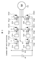
- FIG. 1 is a circuit diagram of an inverter using power semiconductor elements to which the present invention is applied;
- FIG. 1 is a circuit diagram of an inverter employing dual-gate IGBTs to which the present invention is applied;
- FIG. 1 is a circuit diagram of an inverter employing dual-gate IGBTs and MOS-controlled diodes to which the present invention is applied;
- FIG. 1A and 1B are a perspective view and a schematic cross-sectional view showing a wiring structure of a control line according to Example 1 of the present invention;
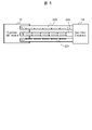
- FIG. It is a figure explaining the principle of this invention.
- FIG. 8 is a perspective view and a schematic cross-sectional view showing a wiring structure of control lines according to Example 2 of the present invention
- 8A and 8B are a perspective view and a schematic cross-sectional view showing a wiring structure of a control line according to Example 3 of the present invention
- FIG. It is a perspective view and a cross-sectional schematic diagram which show the wiring structure of the control line which concerns on Example 4 of this invention.
- FIG. 11 is a perspective view showing a wiring structure of control lines according to Example 5 of the present invention;
- FIG. 1 is a circuit diagram of an inverter using power semiconductor devices to which the present invention is applied.
- FIG. 1 exemplifies a two-level three-phase inverter that performs variable speed control of a three-phase motor 003 as a power converter.
- a high-voltage, high-current three-phase inverter generally uses IGBTs 011g to 032g and diodes 011d to 032d as power semiconductor devices.
- IGBTs 011g to 032g can be switched between conducting and non-conducting states by inputting on/off signals to their gate terminals, thereby controlling the voltage and current of the inverter main circuit.
- the gate signal of the upper arm IGBT 011g is turned on and the lower arm IGBT 012g is turned off, the upper arm is conducting, so the inverter output (terminal) 010 has the same voltage as the input side DC voltage. is output.
- a flywheel diode 011d is connected in parallel with the IGBT 011g. For example, when the IGBT 011g of the upper arm is on and current is flowing from the IGBT 011g to the motor side, the current is commutated to the freewheeling diode 012d of the lower arm when the IGBT 011g is turned off.
- the gate driver gate drive circuit
- gate wiring control line
- the on/off signal of the IGBT is output by the gate driver based on the PWM signal from the microcomputer installed in the control logic unit.
- a means for transmitting the signal of the gate driver to the power semiconductor element is the gate wiring.
- the influence of the magnetic field generated by the current in the main circuit wiring in the inverter also causes unnecessary gate voltage fluctuations, which may cause malfunction of the IGBT.
- the inductance of the gate wiring is large, the time required for the signal of the gate driver to be transmitted to the power semiconductor element becomes long, and the desired inverter output may not be obtained due to this signal delay.
- Fig. 2 is a circuit diagram of an inverter employing dual-gate IGBTs 011gd-032gd to which the present invention is applied.
- multi-gate semiconductor devices namely dual-gate IGBTs 011gd to 032gd, are being put to practical use.
- Each IGBT 011gd to 032gd has a switching gate (first control terminal) Gs, a carrier control gate (second control terminal) Gc, an auxiliary emitter Es, and terminals corresponding to these.
- Each of these terminals is connected to gate drivers 011k to 032k.
- These gate wirings (control lines) 221 to 223 (FIG. 4) need to have low inductance in order to suppress circuit malfunctions and signal delays, like gate wirings for driving conventional IGBTs.
- Fig. 3 is a circuit diagram of an inverter that employs dual-gate IGBTs 011gd-032gd and MOS control diodes 011dm-032dm to which the present invention is applied.
- MOS control diodes 011dm to 032dm are being put into practical use.
- the dual-gate IGBTs 011gd to 032gd illustrated in FIG. 3 the addition of the MOS control gate (third control terminal) Gd results in the gate wiring connecting the semiconductor elements forming each arm and the gate drivers 011k to 032k. It becomes four.
- These gate wirings (control lines) 221 to 224 (FIG. 6) also need to have low inductance, like the gate wirings for driving the IGBT shown in FIG.
- Example 1 is, for example, a wiring structure of control lines for realizing an inverter device employing dual-gate IGBTs 011gd and 012gd in the circuit configuration of FIG. 4A and 4B are a perspective view and a schematic cross-sectional view showing a wiring structure of a control line according to Example 1 of the present invention (hereinafter also referred to as “wiring structure of Example 1”).
- the perspective view is a view with the supporting base and the like removed to explain the shape of one pair of upper and lower arms in the power converter, that is, one phase corresponding to two levels.
- the portion surrounded by a dashed line is a schematic cross-sectional view showing the cross-sectional structure taken along the line AA', which is also a view with the insulating support and the like removed in order to explain the mutual positional relationship.
- Reference numeral 211 in FIG. 4 denotes a module (hereinafter referred to as "IGBT module”) 211 in which a dual gate IGBT 011gd that constitutes the upper arm of the two-level conversion device is mounted, and reference numeral 11 denotes a dual gate IGBT 011gd that constitutes the lower arm. It is a module (hereinafter referred to as "IGBT module”) 11 in which a gate IGBT 012gd is mounted.
- the IGBT module 11 is provided with a collector main terminal 12 and an emitter main terminal 13, which are connected to the main circuit wiring.
- the main circuit wiring is often composed of a plate-shaped conductor (bus bar).
- the collector main terminal 12 of the IGBT module 11 is connected to the emitter main terminal 213 of the IGBT module 211 by one busbar, and the emitter main terminal 13 is connected to the negative potential side of the power supply by another busbar.
- the collector main terminal 212 of the IGBT module 211 is also connected to the high potential side of the power supply by one bus bar.
- the IGBT module 11 is provided with three gate terminals, a gate terminal 121 forming a switching gate Gs, a gate terminal 123 forming a carrier control gate Gc, and an auxiliary emitter Es serving as a reference potential for these terminals. It has an emitter terminal 122 .
- Three gate wiring busbars 221, 222, and 223 corresponding to these three gate terminals are connected. These gate wirings are connected to the gate driver 114 and serve to transmit drive signals from the gate driver 114 to the IGBT module 11 .
- a feature of this first embodiment is that the two gate wiring busbars 221 and 223 are arranged opposite to the auxiliary emitter wiring busbar 222, respectively.
- the auxiliary emitter wiring busbar 222 is arranged to face both the gate wiring busbar 221 and the gate wiring busbar 223 . Since these gate wirings are arranged opposite to each other, a low inductance can be realized by the principle described with reference to FIG.
- FIG. 5 shows a cross-sectional structure of the gate wirings (control lines) 221 to 223 in a direction (longitudinal direction of the gate wirings) perpendicular to the AA' direction in FIG.
- Gate currents Igc and Igs flowing through the gate wiring busbars 221-223 are shown.
- the gate currents Igc and Igs that flow when driving the gates of the IGBTs have waveforms close to impulses, and thus contain many high-frequency components.
- the gate current is caused to flow back and forth through the gate wiring (221, 223) and the auxiliary emitter wiring (222) that are arranged opposite to each other. That is, since the directions of the currents are opposite to each other, the unevenly distributed positions of the currents in the two wires are close to each other. Due to such proximity effects, the current in each conductor flows near surfaces that are close to each other. Also, the gate current Igs for driving the switching gate Gs and the gate current Igc for driving the carrier control gate Gc flow in opposite directions to the auxiliary emitter wiring (222) interposed between them. Therefore, as indicated by the arrows in FIG. 5, the current flows in each conductor in a biased distribution close to the facing surface.
- the Igs of the gate wiring busbar 221 and the gate current Igs in the auxiliary emitter wiring busbar 222 flow close to each other, so the magnetic fluxes generated by these currents are cancelled.
- the gate current Igc in the gate wiring busbar 223 and the gate current Igc in the auxiliary emitter wiring busbar 222 flow close to each other, the magnetic fluxes generated by these currents are cancelled.
- the wiring structure of Example 1 has a low inductance.
- auxiliary emitter wiring for each gate wiring according to the same principle and face each other to cancel the magnetic flux and reduce the inductance.
- the auxiliary emitter wiring is prepared for each gate wiring, which increases the number of wirings and complicates the wiring structure.
- the gate wiring busbar Gs and the gate wiring busbar Gc are arranged on opposite sides farther apart via the auxiliary emitter wiring busbar 222, so that interference between them can be prevented. It is possible to prevent this and realize stable operation of the gate.
- the wiring structure of Example 1 is preferably plate-shaped, and the width W of each wiring busbar and the distance d between the wirings preferably satisfy the condition W>d. By satisfying such conditions, it is possible to sufficiently reduce the inductance value of the wiring.
- each wiring busbar As the material for each wiring busbar, it is desirable to use copper, which has a small skin depth against high-frequency current (current is more concentrated on the surface of the opposing busbar, so the magnetic flux cancellation effect is large and the inductance is small). However, from the viewpoint of weight reduction, even if aluminum is used, the effect is not significantly impaired compared to copper.
- Example 2 is, for example, the wiring structure of the control line for realizing an inverter device employing dual gate IGBTs 011gd to 032gd and MOS control diodes 011dm to 032dm in the circuit configuration of FIG.
- a gate terminal 124 for controlling the MOS control diode 012dm and a gate wiring bus bar 224 are added to the wiring structure of the first embodiment. Since other points are the same as those of the first embodiment, portions having the same effect are denoted by the same reference numerals to avoid duplication of description.
- FIG. 6 is a perspective view and a schematic cross-sectional view showing a wiring structure of a control line according to Example 2 of the present invention (hereinafter also referred to as "wiring structure of Example 2").
- the perspective view is a view with the supporting base and the like removed to explain the shape of one pair of upper and lower arms in the power converter, that is, one phase corresponding to two levels.
- the part surrounded by a broken line is a schematic cross-sectional view showing the cross-sectional structure taken along the line AA', which is also a view with the insulating support and the like removed in order to explain the mutual positional relationship.
- the gate wiring busbar 224 which is a feature of the second embodiment, is connected to the gate drivers 114, 012k through the same route as the gate busbar wirings 221-223 of the first embodiment.
- the gate wiring busbar 224 of the MOS control diode 012dm is arranged outside (on the paper surface) the gate wiring busbar 223 of the dual gate IGBT 012gd.
- the gate wiring that controls the MOS control diode 012dm is also desired to have as low inductance as possible in order to suppress noise and malfunction. Therefore, this gate wiring 224 also has a structure in which it runs parallel to the auxiliary emitter wiring 222 so as to be laminated. However, the gate line 224 has, in between it and the auxiliary emitter line 222, the gate line 223 that drives the dual gate IGBT 012gd. Therefore, the wiring gap between the gate wiring 224 and the auxiliary emitter wiring 222 is widened. Therefore, the gate wiring 224 has a smaller magnetic flux canceling effect due to the reciprocating current, and has a larger inductance than the gate wiring 223 . However, the harm is minimal for the following reasons.
- a comparison of the IGBT 011gd to 032gd gate drive timing and MOS diode control timing in the inverter device is as follows. First, the main circuit voltage (or main circuit current) applied to the IGBTs greatly changes at the timing of turning on or off the gate signals of the IGBTs 011gd to 032gd. On the other hand, at the ON or OFF timings of the MOS control diodes 011dm to 032dm, the main circuit voltage change (or current change) applied to these diodes is very small. Therefore, noise generation induced to the gate wiring at the ON or OFF timing of the MOS control diodes 011dm to 032dm is very small.
- Embodiment 2 In order to minimize the inductance of all gate wiring, it is possible to further increase the auxiliary emitter wiring or add wiring width and run the gate wiring of the MOS diode in parallel. Increased area and volume. In order to prevent this, the structure of Embodiment 2, which can achieve both low inductance and miniaturization, is effective.
- Example 2 the three gate wiring busbars 221, 223, 224 were explained on the assumption that the dual gate IGBTs 011gd, 012gd and the MOS control diodes 011dm, 012dm are used together.
- the gate wiring to which the gate signal that changes the main circuit voltage (or main circuit current) is input should be placed near the auxiliary emitter wiring. By arranging the other gate wiring outside it, it is possible to achieve both low inductance and miniaturization of the gate wiring.
- Embodiment 3 shown in FIG. 7 is characterized in that the control line of Embodiment 2 shown in FIG. 7A and 7B are a perspective view and a schematic cross-sectional view showing a wiring structure of control lines according to a third embodiment of the present invention (hereinafter also referred to as "wiring structure of the third embodiment").
- the gate wiring busbars 221 to 224 themselves are the same as those in the second embodiment, and are made of copper bars or the like. ing.
- the gate wiring busbars 221 to 224 are made of thin copper plates or the like, and if the wiring length is long, they may deform due to gravity, and there is a possibility of short-circuiting between adjacent copper plates. Therefore, as shown in FIG. 7, by sealing and holding with an insulating material 225, the distance between the conductors is maintained, and by providing and fixing a support portion, insulation is secured and the member is supported. is effective.
- Example 4 shown in FIG. 8 is a modification of Example 2 shown in FIG. Compared with the second embodiment, the feature is that the gate wiring of the MOS diode is not stacked with other wiring but runs parallel to the auxiliary emitter wiring.
- 8A and 8B are a perspective view and a schematic cross-sectional view showing a wiring structure of control lines according to a fourth embodiment of the present invention (hereinafter also referred to as "wiring structure of the fourth embodiment").
- a portion surrounded by a broken line in FIG. 8 is a diagram showing a cross-sectional structure taken along line A-A' in FIG.
- the inductance of the gate wirings 221 and 223 on the IGBT side is minimized as in the third embodiment of FIG. , the magnetic flux is weakly canceled and the reduction in inductance is small.
- the inductance of the gate wiring of the diode does not have to be minimized, so the wiring structure of the fourth embodiment hardly impairs the effect.
- FIG. 9 is a perspective view showing a wiring structure of control lines according to Example 5 of the present invention (hereinafter also referred to as "wiring structure of Example 5").
- wiring structure of Example 5" In the first embodiment (FIG. 4) to the fourth embodiment (FIG. 8), the wiring structure of the control line has been mainly described. is exemplified. That is, like the fifth embodiment shown in FIG. 9, it is possible to connect sheet-metal main circuit wirings 311, 312, and 313 directly above the IGBT modules 11 and 211.
- FIG. 9 is a perspective view showing a wiring structure of control lines according to Example 5 of the present invention (hereinafter also referred to as "wiring structure of Example 5").
- the collector terminal of the upper arm module is connected to the main circuit wiring 311 that constitutes the high potential side of the power supply.
- the emitter terminal of the upper arm module and the collector terminal of the lower arm are connected to the main circuit wiring 312 and connected to the motor side as the inverter output (terminal) 010 (FIGS. 1 to 3).
- the emitter terminal of the lower arm module is connected to main circuit wiring 313 which constitutes the low potential side of the power supply.
- These main circuit wirings 311, 312, and 313 constitute one phase of the inverter.
- a gate wiring and an auxiliary emitter wiring made of copper wire may be used as a twisted pair control line.
- the twisted pair control line not only is the twisted pair not twisted in the vicinity of the connection point to each terminal, but the flexible structure causes the untwisting, etc., and there are places where the distance between the two lines is greatly widened. Sometimes. Such locations are susceptible to magnetic flux.
- main circuit wirings 311, 312, 313 are arranged directly above the IGBT modules 11, 211 in order to realize such a configuration more reliably. As a result, the control lines made up of busbars are less susceptible to magnetic flux caused by large currents flowing through the main circuit wirings 311 , 312 , and 313 .
- Laminated busbars are power circuits (electric power converters) that use power semiconductor elements such as IPMs (Intelligent Power Modules) with built-in drive circuits, in addition to IGBTs, to suppress abnormal voltage during high-speed switching and achieve high-speed operation.
- IPMs Intelligent Power Modules
- This is a laminated wiring structure aimed at improving the characteristics for This laminate bus bar can solve the following problems 1 to 4 by forming a multi-layer composite structure by laminating insulating film sheets and metal conductors.
- the laminated busbar achieves low gate wiring inductance in inverters using IGBTs.
- the laminate bus bar has a structure in which plate-shaped conductor bars are used for the gate wiring and the auxiliary emitter wiring, and are arranged opposite to each other with an interval d narrower than the width W of these conductor bars. That is, width W>gap d. It is also possible to realize lightweight laminated busbars using aluminum conductors instead of general copper conductors.
- inverters configured with dual-gate IGBTs 011gd to 032gd and MOS control diodes 011dm to 032dm require more than twice as much wiring as non-IGBT inverters. Therefore, when a laminate bus bar is applied to an inverter using multi-gate semiconductor devices, the volume and area required for the wiring structure become a problem. In addition, as the number of wirings increases, the size of the inverter device (power converter) also increases.
- the wiring structures of Examples 1 to 5 suppress an increase in the volume and area of the gate wiring structure, avoid an increase in the size of the device, and reduce the inductance in a power converter that employs a multi-gate semiconductor element. It is designed so that it can be laid
- the multi-gate semiconductor device is a power semiconductor device having multiple gate control terminals Gs, Gc, Gd, Es, such as dual-gate IGBTs 011gd to 032gd and MOS control diodes 011dm to 032dm.
- This wiring structure is a gate wiring and an auxiliary emitter wiring that connect a multi-gate semiconductor element to a gate driver.
- the multi-gate semiconductor device includes, for example, main terminal pairs such as collector/emitter or drain/source, and gates as a plurality of corresponding control terminals.
- the gate driver controls the control current flowing through the main terminal pair with the control voltage applied to the control terminals.
- This wiring structure is composed of control lines through which a control current flows between the gate driver and the control terminal through a first current path and a second current path.
- the first current path and the second current path are adjacent to each other and laid so as to cancel out the electromagnetic fields formed by the currents flowing through them. According to this wiring structure, the inductance can be evenly reduced.
- the multi-gate semiconductor elements 011gd and 012gd are connected to the first main terminal 212 on the high potential side and the a second main terminal 213, a plurality of control terminals Gs, Gc, Gd, and a control voltage reference terminal Es serving as a reference for the voltage applied to the plurality of control terminals Gs, Gc, Gd.
- control lines 221-224 are suitable for inverters employing dual-gate IGBTs 011gd, 012gd and MOS control diodes 011dm, 012dm shown in the circuit diagram of FIG.
- Each IGBT has, as a plurality of control terminals Gs, Gc, Gd, and Es, a switching gate (first control terminal) Gs, a carrier control gate (second control terminal) Gc, an auxiliary emitter Es, and a MOS It has a control gate (third control terminal) Gd and respective terminals. Each of these terminals is connected to the gate driver 114 .
- a plurality of control terminals Gs, Gc, Gd, and Es are connected as follows. First, the first control terminal Gs is connected to the gate drivers 114, 011k by the plate-shaped first control signal conductor 221. As shown in FIG. Similarly, the second control terminal Gc is also connected to the gate driver 114,011k by a plate-shaped second control signal conductor 223. FIG. Similarly, the control voltage reference terminal Es is also connected to the gate driver 114,011k with a control voltage reference conductor 222 in the form of a plate. The first control signal conductor 221 and the second control signal conductor 223 are placed in close proximity to the control voltage reference conductor 222 .
- each of the conductors 221, 223, 222 is plate-shaped, and each major surface of each large area is arranged in the following mutual positional relationship.
- each conductor 221 , 223 is arranged parallel to the main plane of the control voltage reference conductor 222 .
- the control voltage reference conductor 222 is disposed intermediate the first control signal conductor 221 and the second control signal conductor 223 .
- This wiring structure is suitable for power converters such as inverters. That is, in the inverter that employs the dual gate IGBTs 011gd to 032gd and MOS control diodes 011dm to 032dm shown in the circuit diagram of FIG. However, by arranging the control voltage reference conductor 222 described above between the first control signal conductor 221 and the second control signal conductor 223, an increase in size can be avoided.
- the gate current flows in a reciprocating direction through the gate wiring and the auxiliary emitter wiring which are arranged opposite to each other. That is, since the directions of the currents are opposite to each other, the magnetic fluxes flowing closely between the mutual wirings and generated by these currents are cancelled. Since the magnetic flux is thus canceled for any gate current, the wiring structure can be made to have a low inductance, thereby suppressing circuit malfunction and signal delay.
- each IGBT has a switching gate (first control terminal) Gs, a carrier control gate (second control terminal) Gc, and , an auxiliary emitter Es, and a MOS control gate (third control terminal) Gd, respectively, and these terminals are connected to a gate driver 114 .
- a plurality of control terminals Gs, Gc, Gd, and Es are arranged in the following mutual positional relationship.
- a third control terminal (MOS control gate) Gd is connected to the gate driver 114,011k by a plate-like third control signal conductor 224.
- FIG. The third control signal conductor 224 is arranged adjacent to the first control signal conductor 221 or the second control signal conductor 223 such that their major surfaces are parallel. In this manner, if the plate-like conductors are arranged so that the wide main surfaces face each other, the inductance can be further reduced by the magnetic flux canceling effect of the adjacent reverse currents.
- a third control terminal (MOS control gate) Gd is connected to the gate driver 114, 011k by a plate-like third control signal conductor 224.
- FIG. A third control signal conductor 224 is positioned proximate to the control voltage reference conductor 222 .
- the main surface of the third control signal conductor 224 does not have to be arranged parallel to and opposite to the main surfaces of the other conductors. Therefore, the reverse currents due to the third control signal conductor 224 and the control voltage reference conductor 222 do not come close to each other, the magnetic flux canceling effect of these conductors is small, and the reduction in inductance is small.
- the main circuit voltage change (or current change) applied to the diodes is very small. Therefore, noise generation induced to the gate wiring at the ON or OFF timing of the MOS control diodes 011dm to 032dm is very small.
- the first control signal conductor 221, the second control signal conductor 223, and the control voltage reference conductor 222 are insulating materials (insulators). It is electrically isolated by 225 and held in a sealed manner.
- the wiring structure of Example 3 extends over the entire length of the wire, maintains the distance between the conductors arranged in parallel, ensures insulation, and is fixed by a reliable support.
- the wiring structure of the third embodiment that is, the gate wiring busbars 221 to 224 made of thin copper plates or the like, does not deform due to gravity even when the wiring length is increased, and the adjacent copper plates are short-circuited. Danger can be avoided.
- the first main circuit conductor 311 and the second main circuit conductor 312 are connected to the multi-gate semiconductor elements 011gd and 012gd (FIG. 3). ) was placed directly above the The first main circuit conductor 311 is plate-shaped and is connected to the first main terminal 212 of the multi-gate semiconductor device 011gd.
- the second main circuit conductor 312 is also plate-shaped and is connected to the second main terminal 213 of the multi-gate semiconductor device 011gd.
- the width W of the wiring busbars 221 to 224 and the distance d between the wiring busbars 221 to 224 satisfy the condition W>d. . Satisfying these conditions enhances the effect of enhancing the skin effect and the proximity effect, and the inductance value of each wiring bus bar 221-224 can be sufficiently reduced.
- any one of the wiring structures of [1] to [7] above may be adopted in a railway power converter driven at 1 kV or higher.
- a railway vehicle equipped with such a railway power converter can be controlled with high accuracy, and the power source is stabilized and the motor is driven smoothly, so that the ride comfort is improved.
- the size of the power converter itself can be reduced, the quality performance can be improved, and the ease of production and repair can lead to cost reduction.
Landscapes
- Engineering & Computer Science (AREA)
- Power Engineering (AREA)
- Power Conversion In General (AREA)
Priority Applications (1)
| Application Number | Priority Date | Filing Date | Title |
|---|---|---|---|
| JP2023503595A JP7609966B2 (ja) | 2021-03-03 | 2021-12-28 | 制御線の配線構造、それを有する鉄道用電力変換器、制御線敷設方法 |
Applications Claiming Priority (2)
| Application Number | Priority Date | Filing Date | Title |
|---|---|---|---|
| JP2021-033894 | 2021-03-03 | ||
| JP2021033894 | 2021-03-03 |
Publications (1)
| Publication Number | Publication Date |
|---|---|
| WO2022185703A1 true WO2022185703A1 (ja) | 2022-09-09 |
Family
ID=83153981
Family Applications (1)
| Application Number | Title | Priority Date | Filing Date |
|---|---|---|---|
| PCT/JP2021/048975 Ceased WO2022185703A1 (ja) | 2021-03-03 | 2021-12-28 | 制御線の配線構造、それを有する鉄道用電力変換器、制御線敷設方法 |
Country Status (2)
| Country | Link |
|---|---|
| JP (1) | JP7609966B2 (https=) |
| WO (1) | WO2022185703A1 (https=) |
Citations (2)
| Publication number | Priority date | Publication date | Assignee | Title |
|---|---|---|---|---|
| WO2019044832A1 (ja) * | 2017-08-30 | 2019-03-07 | 株式会社日立製作所 | 電力変換装置及び電力変換方法 |
| JP2019161720A (ja) * | 2018-03-08 | 2019-09-19 | 株式会社日立製作所 | インバータ装置 |
-
2021
- 2021-12-28 WO PCT/JP2021/048975 patent/WO2022185703A1/ja not_active Ceased
- 2021-12-28 JP JP2023503595A patent/JP7609966B2/ja active Active
Patent Citations (2)
| Publication number | Priority date | Publication date | Assignee | Title |
|---|---|---|---|---|
| WO2019044832A1 (ja) * | 2017-08-30 | 2019-03-07 | 株式会社日立製作所 | 電力変換装置及び電力変換方法 |
| JP2019161720A (ja) * | 2018-03-08 | 2019-09-19 | 株式会社日立製作所 | インバータ装置 |
Also Published As
| Publication number | Publication date |
|---|---|
| JPWO2022185703A1 (https=) | 2022-09-09 |
| JP7609966B2 (ja) | 2025-01-07 |
Similar Documents
| Publication | Publication Date | Title |
|---|---|---|
| US8519561B2 (en) | Power module and vehicle-mounted inverter using the same | |
| US10141254B1 (en) | Direct bonded copper power module with elevated common source inductance | |
| EP1758440B1 (en) | Semiconductor device | |
| CN110710341B (zh) | 变换器的功率相模块、变换器和车辆 | |
| US11128235B2 (en) | Power conversion device | |
| US10554123B2 (en) | Power converter with a parallel flat plate conductor electrically connected with a capacitor and a power module | |
| JP2016220356A (ja) | 電力変換装置 | |
| EP3745579B1 (en) | Power conversion device and electric railroad vehicle equipped with power conversion device | |
| JP3896940B2 (ja) | 半導体装置 | |
| JP3793700B2 (ja) | 電力変換装置 | |
| US11394310B2 (en) | Power conversion device | |
| JP7364103B2 (ja) | 電力変換装置 | |
| JP6720601B2 (ja) | 電力変換装置 | |
| JP7609966B2 (ja) | 制御線の配線構造、それを有する鉄道用電力変換器、制御線敷設方法 | |
| JP7840793B2 (ja) | 電力変換装置 | |
| JP7716346B2 (ja) | 半導体装置および半導体装置を備えたインバータ | |
| WO2022107439A1 (ja) | パワー半導体モジュール | |
| CN107710576A (zh) | 具有并联连接的半导体开关的功率换流器 | |
| JP7851262B2 (ja) | 電力変換装置 | |
| US12323070B2 (en) | Power conversion device | |
| JP7756842B2 (ja) | 電力変換装置 | |
| JP7559189B1 (ja) | 電力変換装置 | |
| JP6698968B1 (ja) | 半導体装置および電力変換装置 | |
| WO2025257935A1 (ja) | 半導体装置および電力変換装置 | |
| JP2019017142A (ja) | 電力変換装置 |
Legal Events
| Date | Code | Title | Description |
|---|---|---|---|
| 121 | Ep: the epo has been informed by wipo that ep was designated in this application |
Ref document number: 21929259 Country of ref document: EP Kind code of ref document: A1 |
|
| DPE1 | Request for preliminary examination filed after expiration of 19th month from priority date (pct application filed from 20040101) | ||
| WWE | Wipo information: entry into national phase |
Ref document number: 2023503595 Country of ref document: JP |
|
| NENP | Non-entry into the national phase |
Ref country code: DE |
|
| 122 | Ep: pct application non-entry in european phase |
Ref document number: 21929259 Country of ref document: EP Kind code of ref document: A1 |