WO2022185703A1 - Control line wiring structure, railway power converter having same, and control line laying method - Google Patents
Control line wiring structure, railway power converter having same, and control line laying method Download PDFInfo
- Publication number
- WO2022185703A1 WO2022185703A1 PCT/JP2021/048975 JP2021048975W WO2022185703A1 WO 2022185703 A1 WO2022185703 A1 WO 2022185703A1 JP 2021048975 W JP2021048975 W JP 2021048975W WO 2022185703 A1 WO2022185703 A1 WO 2022185703A1
- Authority
- WO
- WIPO (PCT)
- Prior art keywords
- control
- gate
- terminal
- conductor
- signal conductor
- Prior art date
Links
- 238000000034 method Methods 0.000 title claims description 11
- 239000004065 semiconductor Substances 0.000 claims abstract description 39
- 230000005672 electromagnetic field Effects 0.000 claims abstract description 5
- 239000004020 conductor Substances 0.000 claims description 101
- 239000012212 insulator Substances 0.000 claims description 4
- 230000004907 flux Effects 0.000 description 17
- 230000000694 effects Effects 0.000 description 11
- 238000010586 diagram Methods 0.000 description 10
- 230000009977 dual effect Effects 0.000 description 10
- RYGMFSIKBFXOCR-UHFFFAOYSA-N Copper Chemical compound [Cu] RYGMFSIKBFXOCR-UHFFFAOYSA-N 0.000 description 9
- 229910052802 copper Inorganic materials 0.000 description 8
- 239000010949 copper Substances 0.000 description 8
- 230000007257 malfunction Effects 0.000 description 6
- 230000009467 reduction Effects 0.000 description 6
- 230000008859 change Effects 0.000 description 5
- 230000002500 effect on skin Effects 0.000 description 3
- 229910052782 aluminium Inorganic materials 0.000 description 2
- XAGFODPZIPBFFR-UHFFFAOYSA-N aluminium Chemical compound [Al] XAGFODPZIPBFFR-UHFFFAOYSA-N 0.000 description 2
- 230000008901 benefit Effects 0.000 description 2
- 230000001934 delay Effects 0.000 description 2
- 230000005484 gravity Effects 0.000 description 2
- 239000011810 insulating material Substances 0.000 description 2
- 238000009413 insulation Methods 0.000 description 2
- 229910052751 metal Inorganic materials 0.000 description 2
- 239000002184 metal Substances 0.000 description 2
- 230000002159 abnormal effect Effects 0.000 description 1
- 239000003990 capacitor Substances 0.000 description 1
- 238000006243 chemical reaction Methods 0.000 description 1
- 239000002131 composite material Substances 0.000 description 1
- 238000011109 contamination Methods 0.000 description 1
- 238000009826 distribution Methods 0.000 description 1
- 238000005516 engineering process Methods 0.000 description 1
- 230000002708 enhancing effect Effects 0.000 description 1
- 238000009499 grossing Methods 0.000 description 1
- 230000001771 impaired effect Effects 0.000 description 1
- 238000010030 laminating Methods 0.000 description 1
- 238000004519 manufacturing process Methods 0.000 description 1
- 239000000463 material Substances 0.000 description 1
- 230000004048 modification Effects 0.000 description 1
- 238000012986 modification Methods 0.000 description 1
- 238000010248 power generation Methods 0.000 description 1
- 230000008439 repair process Effects 0.000 description 1
- 230000004044 response Effects 0.000 description 1
- 238000007789 sealing Methods 0.000 description 1
- 238000004904 shortening Methods 0.000 description 1
- 230000000087 stabilizing effect Effects 0.000 description 1
- 239000013589 supplement Substances 0.000 description 1
- 239000013585 weight reducing agent Substances 0.000 description 1
Images


Classifications
-
- H—ELECTRICITY
- H02—GENERATION; CONVERSION OR DISTRIBUTION OF ELECTRIC POWER
- H02M—APPARATUS FOR CONVERSION BETWEEN AC AND AC, BETWEEN AC AND DC, OR BETWEEN DC AND DC, AND FOR USE WITH MAINS OR SIMILAR POWER SUPPLY SYSTEMS; CONVERSION OF DC OR AC INPUT POWER INTO SURGE OUTPUT POWER; CONTROL OR REGULATION THEREOF
- H02M1/00—Details of apparatus for conversion
- H02M1/08—Circuits specially adapted for the generation of control voltages for semiconductor devices incorporated in static converters
-
- H—ELECTRICITY
- H02—GENERATION; CONVERSION OR DISTRIBUTION OF ELECTRIC POWER
- H02M—APPARATUS FOR CONVERSION BETWEEN AC AND AC, BETWEEN AC AND DC, OR BETWEEN DC AND DC, AND FOR USE WITH MAINS OR SIMILAR POWER SUPPLY SYSTEMS; CONVERSION OF DC OR AC INPUT POWER INTO SURGE OUTPUT POWER; CONTROL OR REGULATION THEREOF
- H02M7/00—Conversion of ac power input into dc power output; Conversion of dc power input into ac power output
- H02M7/42—Conversion of dc power input into ac power output without possibility of reversal
- H02M7/44—Conversion of dc power input into ac power output without possibility of reversal by static converters
- H02M7/48—Conversion of dc power input into ac power output without possibility of reversal by static converters using discharge tubes with control electrode or semiconductor devices with control electrode
Definitions
- the present invention relates to a control line wiring structure, a railway power converter having the same, and a control line laying method.
- IGBTs Insulated Gate Bipolar Transistors
- Patent Document 1 describes a dual-gate IGBT.
- a dual-gate IGBT is a power semiconductor device having two gate terminals (switching gate Gs and carrier control gate Gc) for one collector terminal and one emitter terminal. By controlling the gate signals input to the two gate terminals, switching loss can be reduced compared to conventional IGBTs.
- Another example is a MOS controlled diode described in Patent Document 2.
- the diode is provided with an insulated gate Gd with a MOS structure, and by applying this gate voltage, the amount of internal charge can be controlled in the MOS controlled diode.
- control lines the gate wiring and the auxiliary emitter wiring (hereinafter, both are collectively referred to as "control lines") are placed close to each other, and sometimes they are twisted together. Furthermore, in the case of multi-gate IGBTs, since there are multiple gate wirings, it is difficult in terms of layout to place all the gate wirings and auxiliary emitter wirings adjacent to each other at the same distance, simply by placing them adjacent to the auxiliary emitter wiring. difference in inductance occurs.
- An object of the present invention is to provide a wiring structure for control lines in which the inductance is evenly reduced.
- the present invention for solving the above problems is a multi-gate semiconductor device having a main terminal pair and a plurality of control terminals for controlling the current flowing through the main terminal pair.
- a wiring structure of a control line connecting between a gate driver for controlling The first current path and the second current path were laid adjacent to each other so as to cancel out the electromagnetic fields created by the respective currents.
- FIG. 1 is a circuit diagram of an inverter using power semiconductor elements to which the present invention is applied;
- FIG. 1 is a circuit diagram of an inverter employing dual-gate IGBTs to which the present invention is applied;
- FIG. 1 is a circuit diagram of an inverter employing dual-gate IGBTs and MOS-controlled diodes to which the present invention is applied;
- FIG. 1A and 1B are a perspective view and a schematic cross-sectional view showing a wiring structure of a control line according to Example 1 of the present invention;
- FIG. It is a figure explaining the principle of this invention.
- FIG. 8 is a perspective view and a schematic cross-sectional view showing a wiring structure of control lines according to Example 2 of the present invention
- 8A and 8B are a perspective view and a schematic cross-sectional view showing a wiring structure of a control line according to Example 3 of the present invention
- FIG. It is a perspective view and a cross-sectional schematic diagram which show the wiring structure of the control line which concerns on Example 4 of this invention.
- FIG. 11 is a perspective view showing a wiring structure of control lines according to Example 5 of the present invention;
- FIG. 1 is a circuit diagram of an inverter using power semiconductor devices to which the present invention is applied.
- FIG. 1 exemplifies a two-level three-phase inverter that performs variable speed control of a three-phase motor 003 as a power converter.
- a high-voltage, high-current three-phase inverter generally uses IGBTs 011g to 032g and diodes 011d to 032d as power semiconductor devices.
- IGBTs 011g to 032g can be switched between conducting and non-conducting states by inputting on/off signals to their gate terminals, thereby controlling the voltage and current of the inverter main circuit.
- the gate signal of the upper arm IGBT 011g is turned on and the lower arm IGBT 012g is turned off, the upper arm is conducting, so the inverter output (terminal) 010 has the same voltage as the input side DC voltage. is output.
- a flywheel diode 011d is connected in parallel with the IGBT 011g. For example, when the IGBT 011g of the upper arm is on and current is flowing from the IGBT 011g to the motor side, the current is commutated to the freewheeling diode 012d of the lower arm when the IGBT 011g is turned off.
- the gate driver gate drive circuit
- gate wiring control line
- the on/off signal of the IGBT is output by the gate driver based on the PWM signal from the microcomputer installed in the control logic unit.
- a means for transmitting the signal of the gate driver to the power semiconductor element is the gate wiring.
- the influence of the magnetic field generated by the current in the main circuit wiring in the inverter also causes unnecessary gate voltage fluctuations, which may cause malfunction of the IGBT.
- the inductance of the gate wiring is large, the time required for the signal of the gate driver to be transmitted to the power semiconductor element becomes long, and the desired inverter output may not be obtained due to this signal delay.
- Fig. 2 is a circuit diagram of an inverter employing dual-gate IGBTs 011gd-032gd to which the present invention is applied.
- multi-gate semiconductor devices namely dual-gate IGBTs 011gd to 032gd, are being put to practical use.
- Each IGBT 011gd to 032gd has a switching gate (first control terminal) Gs, a carrier control gate (second control terminal) Gc, an auxiliary emitter Es, and terminals corresponding to these.
- Each of these terminals is connected to gate drivers 011k to 032k.
- These gate wirings (control lines) 221 to 223 (FIG. 4) need to have low inductance in order to suppress circuit malfunctions and signal delays, like gate wirings for driving conventional IGBTs.
- Fig. 3 is a circuit diagram of an inverter that employs dual-gate IGBTs 011gd-032gd and MOS control diodes 011dm-032dm to which the present invention is applied.
- MOS control diodes 011dm to 032dm are being put into practical use.
- the dual-gate IGBTs 011gd to 032gd illustrated in FIG. 3 the addition of the MOS control gate (third control terminal) Gd results in the gate wiring connecting the semiconductor elements forming each arm and the gate drivers 011k to 032k. It becomes four.
- These gate wirings (control lines) 221 to 224 (FIG. 6) also need to have low inductance, like the gate wirings for driving the IGBT shown in FIG.
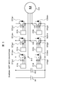
- Example 1 is, for example, a wiring structure of control lines for realizing an inverter device employing dual-gate IGBTs 011gd and 012gd in the circuit configuration of FIG. 4A and 4B are a perspective view and a schematic cross-sectional view showing a wiring structure of a control line according to Example 1 of the present invention (hereinafter also referred to as “wiring structure of Example 1”).
- the perspective view is a view with the supporting base and the like removed to explain the shape of one pair of upper and lower arms in the power converter, that is, one phase corresponding to two levels.
- the portion surrounded by a dashed line is a schematic cross-sectional view showing the cross-sectional structure taken along the line AA', which is also a view with the insulating support and the like removed in order to explain the mutual positional relationship.
- Reference numeral 211 in FIG. 4 denotes a module (hereinafter referred to as "IGBT module”) 211 in which a dual gate IGBT 011gd that constitutes the upper arm of the two-level conversion device is mounted, and reference numeral 11 denotes a dual gate IGBT 011gd that constitutes the lower arm. It is a module (hereinafter referred to as "IGBT module”) 11 in which a gate IGBT 012gd is mounted.
- the IGBT module 11 is provided with a collector main terminal 12 and an emitter main terminal 13, which are connected to the main circuit wiring.
- the main circuit wiring is often composed of a plate-shaped conductor (bus bar).
- the collector main terminal 12 of the IGBT module 11 is connected to the emitter main terminal 213 of the IGBT module 211 by one busbar, and the emitter main terminal 13 is connected to the negative potential side of the power supply by another busbar.
- the collector main terminal 212 of the IGBT module 211 is also connected to the high potential side of the power supply by one bus bar.
- the IGBT module 11 is provided with three gate terminals, a gate terminal 121 forming a switching gate Gs, a gate terminal 123 forming a carrier control gate Gc, and an auxiliary emitter Es serving as a reference potential for these terminals. It has an emitter terminal 122 .
- Three gate wiring busbars 221, 222, and 223 corresponding to these three gate terminals are connected. These gate wirings are connected to the gate driver 114 and serve to transmit drive signals from the gate driver 114 to the IGBT module 11 .
- a feature of this first embodiment is that the two gate wiring busbars 221 and 223 are arranged opposite to the auxiliary emitter wiring busbar 222, respectively.
- the auxiliary emitter wiring busbar 222 is arranged to face both the gate wiring busbar 221 and the gate wiring busbar 223 . Since these gate wirings are arranged opposite to each other, a low inductance can be realized by the principle described with reference to FIG.
- FIG. 5 shows a cross-sectional structure of the gate wirings (control lines) 221 to 223 in a direction (longitudinal direction of the gate wirings) perpendicular to the AA' direction in FIG.
- Gate currents Igc and Igs flowing through the gate wiring busbars 221-223 are shown.
- the gate currents Igc and Igs that flow when driving the gates of the IGBTs have waveforms close to impulses, and thus contain many high-frequency components.
- the gate current is caused to flow back and forth through the gate wiring (221, 223) and the auxiliary emitter wiring (222) that are arranged opposite to each other. That is, since the directions of the currents are opposite to each other, the unevenly distributed positions of the currents in the two wires are close to each other. Due to such proximity effects, the current in each conductor flows near surfaces that are close to each other. Also, the gate current Igs for driving the switching gate Gs and the gate current Igc for driving the carrier control gate Gc flow in opposite directions to the auxiliary emitter wiring (222) interposed between them. Therefore, as indicated by the arrows in FIG. 5, the current flows in each conductor in a biased distribution close to the facing surface.
- the Igs of the gate wiring busbar 221 and the gate current Igs in the auxiliary emitter wiring busbar 222 flow close to each other, so the magnetic fluxes generated by these currents are cancelled.
- the gate current Igc in the gate wiring busbar 223 and the gate current Igc in the auxiliary emitter wiring busbar 222 flow close to each other, the magnetic fluxes generated by these currents are cancelled.
- the wiring structure of Example 1 has a low inductance.
- auxiliary emitter wiring for each gate wiring according to the same principle and face each other to cancel the magnetic flux and reduce the inductance.
- the auxiliary emitter wiring is prepared for each gate wiring, which increases the number of wirings and complicates the wiring structure.
- the gate wiring busbar Gs and the gate wiring busbar Gc are arranged on opposite sides farther apart via the auxiliary emitter wiring busbar 222, so that interference between them can be prevented. It is possible to prevent this and realize stable operation of the gate.
- the wiring structure of Example 1 is preferably plate-shaped, and the width W of each wiring busbar and the distance d between the wirings preferably satisfy the condition W>d. By satisfying such conditions, it is possible to sufficiently reduce the inductance value of the wiring.
- each wiring busbar As the material for each wiring busbar, it is desirable to use copper, which has a small skin depth against high-frequency current (current is more concentrated on the surface of the opposing busbar, so the magnetic flux cancellation effect is large and the inductance is small). However, from the viewpoint of weight reduction, even if aluminum is used, the effect is not significantly impaired compared to copper.
- Example 2 is, for example, the wiring structure of the control line for realizing an inverter device employing dual gate IGBTs 011gd to 032gd and MOS control diodes 011dm to 032dm in the circuit configuration of FIG.
- a gate terminal 124 for controlling the MOS control diode 012dm and a gate wiring bus bar 224 are added to the wiring structure of the first embodiment. Since other points are the same as those of the first embodiment, portions having the same effect are denoted by the same reference numerals to avoid duplication of description.
- FIG. 6 is a perspective view and a schematic cross-sectional view showing a wiring structure of a control line according to Example 2 of the present invention (hereinafter also referred to as "wiring structure of Example 2").
- the perspective view is a view with the supporting base and the like removed to explain the shape of one pair of upper and lower arms in the power converter, that is, one phase corresponding to two levels.
- the part surrounded by a broken line is a schematic cross-sectional view showing the cross-sectional structure taken along the line AA', which is also a view with the insulating support and the like removed in order to explain the mutual positional relationship.
- the gate wiring busbar 224 which is a feature of the second embodiment, is connected to the gate drivers 114, 012k through the same route as the gate busbar wirings 221-223 of the first embodiment.
- the gate wiring busbar 224 of the MOS control diode 012dm is arranged outside (on the paper surface) the gate wiring busbar 223 of the dual gate IGBT 012gd.
- the gate wiring that controls the MOS control diode 012dm is also desired to have as low inductance as possible in order to suppress noise and malfunction. Therefore, this gate wiring 224 also has a structure in which it runs parallel to the auxiliary emitter wiring 222 so as to be laminated. However, the gate line 224 has, in between it and the auxiliary emitter line 222, the gate line 223 that drives the dual gate IGBT 012gd. Therefore, the wiring gap between the gate wiring 224 and the auxiliary emitter wiring 222 is widened. Therefore, the gate wiring 224 has a smaller magnetic flux canceling effect due to the reciprocating current, and has a larger inductance than the gate wiring 223 . However, the harm is minimal for the following reasons.
- a comparison of the IGBT 011gd to 032gd gate drive timing and MOS diode control timing in the inverter device is as follows. First, the main circuit voltage (or main circuit current) applied to the IGBTs greatly changes at the timing of turning on or off the gate signals of the IGBTs 011gd to 032gd. On the other hand, at the ON or OFF timings of the MOS control diodes 011dm to 032dm, the main circuit voltage change (or current change) applied to these diodes is very small. Therefore, noise generation induced to the gate wiring at the ON or OFF timing of the MOS control diodes 011dm to 032dm is very small.
- Embodiment 2 In order to minimize the inductance of all gate wiring, it is possible to further increase the auxiliary emitter wiring or add wiring width and run the gate wiring of the MOS diode in parallel. Increased area and volume. In order to prevent this, the structure of Embodiment 2, which can achieve both low inductance and miniaturization, is effective.
- Example 2 the three gate wiring busbars 221, 223, 224 were explained on the assumption that the dual gate IGBTs 011gd, 012gd and the MOS control diodes 011dm, 012dm are used together.
- the gate wiring to which the gate signal that changes the main circuit voltage (or main circuit current) is input should be placed near the auxiliary emitter wiring. By arranging the other gate wiring outside it, it is possible to achieve both low inductance and miniaturization of the gate wiring.
- Embodiment 3 shown in FIG. 7 is characterized in that the control line of Embodiment 2 shown in FIG. 7A and 7B are a perspective view and a schematic cross-sectional view showing a wiring structure of control lines according to a third embodiment of the present invention (hereinafter also referred to as "wiring structure of the third embodiment").
- the gate wiring busbars 221 to 224 themselves are the same as those in the second embodiment, and are made of copper bars or the like. ing.
- the gate wiring busbars 221 to 224 are made of thin copper plates or the like, and if the wiring length is long, they may deform due to gravity, and there is a possibility of short-circuiting between adjacent copper plates. Therefore, as shown in FIG. 7, by sealing and holding with an insulating material 225, the distance between the conductors is maintained, and by providing and fixing a support portion, insulation is secured and the member is supported. is effective.
- Example 4 shown in FIG. 8 is a modification of Example 2 shown in FIG. Compared with the second embodiment, the feature is that the gate wiring of the MOS diode is not stacked with other wiring but runs parallel to the auxiliary emitter wiring.
- 8A and 8B are a perspective view and a schematic cross-sectional view showing a wiring structure of control lines according to a fourth embodiment of the present invention (hereinafter also referred to as "wiring structure of the fourth embodiment").
- a portion surrounded by a broken line in FIG. 8 is a diagram showing a cross-sectional structure taken along line A-A' in FIG.
- the inductance of the gate wirings 221 and 223 on the IGBT side is minimized as in the third embodiment of FIG. , the magnetic flux is weakly canceled and the reduction in inductance is small.
- the inductance of the gate wiring of the diode does not have to be minimized, so the wiring structure of the fourth embodiment hardly impairs the effect.
- FIG. 9 is a perspective view showing a wiring structure of control lines according to Example 5 of the present invention (hereinafter also referred to as "wiring structure of Example 5").
- wiring structure of Example 5" In the first embodiment (FIG. 4) to the fourth embodiment (FIG. 8), the wiring structure of the control line has been mainly described. is exemplified. That is, like the fifth embodiment shown in FIG. 9, it is possible to connect sheet-metal main circuit wirings 311, 312, and 313 directly above the IGBT modules 11 and 211.
- FIG. 9 is a perspective view showing a wiring structure of control lines according to Example 5 of the present invention (hereinafter also referred to as "wiring structure of Example 5").
- the collector terminal of the upper arm module is connected to the main circuit wiring 311 that constitutes the high potential side of the power supply.
- the emitter terminal of the upper arm module and the collector terminal of the lower arm are connected to the main circuit wiring 312 and connected to the motor side as the inverter output (terminal) 010 (FIGS. 1 to 3).
- the emitter terminal of the lower arm module is connected to main circuit wiring 313 which constitutes the low potential side of the power supply.
- These main circuit wirings 311, 312, and 313 constitute one phase of the inverter.
- a gate wiring and an auxiliary emitter wiring made of copper wire may be used as a twisted pair control line.
- the twisted pair control line not only is the twisted pair not twisted in the vicinity of the connection point to each terminal, but the flexible structure causes the untwisting, etc., and there are places where the distance between the two lines is greatly widened. Sometimes. Such locations are susceptible to magnetic flux.
- main circuit wirings 311, 312, 313 are arranged directly above the IGBT modules 11, 211 in order to realize such a configuration more reliably. As a result, the control lines made up of busbars are less susceptible to magnetic flux caused by large currents flowing through the main circuit wirings 311 , 312 , and 313 .
- Laminated busbars are power circuits (electric power converters) that use power semiconductor elements such as IPMs (Intelligent Power Modules) with built-in drive circuits, in addition to IGBTs, to suppress abnormal voltage during high-speed switching and achieve high-speed operation.
- IPMs Intelligent Power Modules
- This is a laminated wiring structure aimed at improving the characteristics for This laminate bus bar can solve the following problems 1 to 4 by forming a multi-layer composite structure by laminating insulating film sheets and metal conductors.
- the laminated busbar achieves low gate wiring inductance in inverters using IGBTs.
- the laminate bus bar has a structure in which plate-shaped conductor bars are used for the gate wiring and the auxiliary emitter wiring, and are arranged opposite to each other with an interval d narrower than the width W of these conductor bars. That is, width W>gap d. It is also possible to realize lightweight laminated busbars using aluminum conductors instead of general copper conductors.
- inverters configured with dual-gate IGBTs 011gd to 032gd and MOS control diodes 011dm to 032dm require more than twice as much wiring as non-IGBT inverters. Therefore, when a laminate bus bar is applied to an inverter using multi-gate semiconductor devices, the volume and area required for the wiring structure become a problem. In addition, as the number of wirings increases, the size of the inverter device (power converter) also increases.
- the wiring structures of Examples 1 to 5 suppress an increase in the volume and area of the gate wiring structure, avoid an increase in the size of the device, and reduce the inductance in a power converter that employs a multi-gate semiconductor element. It is designed so that it can be laid
- the multi-gate semiconductor device is a power semiconductor device having multiple gate control terminals Gs, Gc, Gd, Es, such as dual-gate IGBTs 011gd to 032gd and MOS control diodes 011dm to 032dm.
- This wiring structure is a gate wiring and an auxiliary emitter wiring that connect a multi-gate semiconductor element to a gate driver.
- the multi-gate semiconductor device includes, for example, main terminal pairs such as collector/emitter or drain/source, and gates as a plurality of corresponding control terminals.
- the gate driver controls the control current flowing through the main terminal pair with the control voltage applied to the control terminals.
- This wiring structure is composed of control lines through which a control current flows between the gate driver and the control terminal through a first current path and a second current path.
- the first current path and the second current path are adjacent to each other and laid so as to cancel out the electromagnetic fields formed by the currents flowing through them. According to this wiring structure, the inductance can be evenly reduced.
- the multi-gate semiconductor elements 011gd and 012gd are connected to the first main terminal 212 on the high potential side and the a second main terminal 213, a plurality of control terminals Gs, Gc, Gd, and a control voltage reference terminal Es serving as a reference for the voltage applied to the plurality of control terminals Gs, Gc, Gd.
- control lines 221-224 are suitable for inverters employing dual-gate IGBTs 011gd, 012gd and MOS control diodes 011dm, 012dm shown in the circuit diagram of FIG.
- Each IGBT has, as a plurality of control terminals Gs, Gc, Gd, and Es, a switching gate (first control terminal) Gs, a carrier control gate (second control terminal) Gc, an auxiliary emitter Es, and a MOS It has a control gate (third control terminal) Gd and respective terminals. Each of these terminals is connected to the gate driver 114 .
- a plurality of control terminals Gs, Gc, Gd, and Es are connected as follows. First, the first control terminal Gs is connected to the gate drivers 114, 011k by the plate-shaped first control signal conductor 221. As shown in FIG. Similarly, the second control terminal Gc is also connected to the gate driver 114,011k by a plate-shaped second control signal conductor 223. FIG. Similarly, the control voltage reference terminal Es is also connected to the gate driver 114,011k with a control voltage reference conductor 222 in the form of a plate. The first control signal conductor 221 and the second control signal conductor 223 are placed in close proximity to the control voltage reference conductor 222 .
- each of the conductors 221, 223, 222 is plate-shaped, and each major surface of each large area is arranged in the following mutual positional relationship.
- each conductor 221 , 223 is arranged parallel to the main plane of the control voltage reference conductor 222 .
- the control voltage reference conductor 222 is disposed intermediate the first control signal conductor 221 and the second control signal conductor 223 .
- This wiring structure is suitable for power converters such as inverters. That is, in the inverter that employs the dual gate IGBTs 011gd to 032gd and MOS control diodes 011dm to 032dm shown in the circuit diagram of FIG. However, by arranging the control voltage reference conductor 222 described above between the first control signal conductor 221 and the second control signal conductor 223, an increase in size can be avoided.
- the gate current flows in a reciprocating direction through the gate wiring and the auxiliary emitter wiring which are arranged opposite to each other. That is, since the directions of the currents are opposite to each other, the magnetic fluxes flowing closely between the mutual wirings and generated by these currents are cancelled. Since the magnetic flux is thus canceled for any gate current, the wiring structure can be made to have a low inductance, thereby suppressing circuit malfunction and signal delay.
- each IGBT has a switching gate (first control terminal) Gs, a carrier control gate (second control terminal) Gc, and , an auxiliary emitter Es, and a MOS control gate (third control terminal) Gd, respectively, and these terminals are connected to a gate driver 114 .
- a plurality of control terminals Gs, Gc, Gd, and Es are arranged in the following mutual positional relationship.
- a third control terminal (MOS control gate) Gd is connected to the gate driver 114,011k by a plate-like third control signal conductor 224.
- FIG. The third control signal conductor 224 is arranged adjacent to the first control signal conductor 221 or the second control signal conductor 223 such that their major surfaces are parallel. In this manner, if the plate-like conductors are arranged so that the wide main surfaces face each other, the inductance can be further reduced by the magnetic flux canceling effect of the adjacent reverse currents.
- a third control terminal (MOS control gate) Gd is connected to the gate driver 114, 011k by a plate-like third control signal conductor 224.
- FIG. A third control signal conductor 224 is positioned proximate to the control voltage reference conductor 222 .
- the main surface of the third control signal conductor 224 does not have to be arranged parallel to and opposite to the main surfaces of the other conductors. Therefore, the reverse currents due to the third control signal conductor 224 and the control voltage reference conductor 222 do not come close to each other, the magnetic flux canceling effect of these conductors is small, and the reduction in inductance is small.
- the main circuit voltage change (or current change) applied to the diodes is very small. Therefore, noise generation induced to the gate wiring at the ON or OFF timing of the MOS control diodes 011dm to 032dm is very small.
- the first control signal conductor 221, the second control signal conductor 223, and the control voltage reference conductor 222 are insulating materials (insulators). It is electrically isolated by 225 and held in a sealed manner.
- the wiring structure of Example 3 extends over the entire length of the wire, maintains the distance between the conductors arranged in parallel, ensures insulation, and is fixed by a reliable support.
- the wiring structure of the third embodiment that is, the gate wiring busbars 221 to 224 made of thin copper plates or the like, does not deform due to gravity even when the wiring length is increased, and the adjacent copper plates are short-circuited. Danger can be avoided.
- the first main circuit conductor 311 and the second main circuit conductor 312 are connected to the multi-gate semiconductor elements 011gd and 012gd (FIG. 3). ) was placed directly above the The first main circuit conductor 311 is plate-shaped and is connected to the first main terminal 212 of the multi-gate semiconductor device 011gd.
- the second main circuit conductor 312 is also plate-shaped and is connected to the second main terminal 213 of the multi-gate semiconductor device 011gd.
- the width W of the wiring busbars 221 to 224 and the distance d between the wiring busbars 221 to 224 satisfy the condition W>d. . Satisfying these conditions enhances the effect of enhancing the skin effect and the proximity effect, and the inductance value of each wiring bus bar 221-224 can be sufficiently reduced.
- any one of the wiring structures of [1] to [7] above may be adopted in a railway power converter driven at 1 kV or higher.
- a railway vehicle equipped with such a railway power converter can be controlled with high accuracy, and the power source is stabilized and the motor is driven smoothly, so that the ride comfort is improved.
- the size of the power converter itself can be reduced, the quality performance can be improved, and the ease of production and repair can lead to cost reduction.
Abstract
Provided is a control line wiring structure that connects between a multi-gate semiconductor element and a gate driver, said multi-gate semiconductor element having a main terminal pair and a plurality of control terminals that control the current flowing through the main terminal pair, said gate driver using control voltages applied to the control terminals to control the current flowing through the main terminal pair. The control line wiring structure has first and second current paths connected between terminals including the control terminals and the gate driver, wherein the first and second current paths are laid adjacently to each other so that the electromagnetic fields formed by the currents flowing therethrough are canceled by each other.
Description
本発明は、制御線の配線構造、それを有する鉄道用電力変換器、制御線敷設方法に関する。
The present invention relates to a control line wiring structure, a railway power converter having the same, and a control line laying method.
近年、鉄道や電気自動車、風力発電等のパワーエレクトロニクス機器には交流と直流、あるいは交流と交流の間で電力を変換する電力変換器が広く使われている。この電力変換器には高電圧・大電流の制御が可能なパワーデバイスと呼ばれる半導体素子が使われており、特に高電圧の電力変換器にはIGBT(Insulated Gate Bipolar Transistor)と呼ばれるパワーデバイスが使われている。IGBTは、高速スイッチングが可能というMOSゲートデバイスの長所と、導通抵抗が小さいというバイポーラデバイスの長所を併せ持つ半導体素子である。
In recent years, power converters that convert power between AC and DC, or between AC and AC, are widely used in power electronics equipment such as railways, electric vehicles, and wind power generation. These power converters use semiconductor elements called power devices that can control high voltages and large currents. In particular, high-voltage power converters use power devices called IGBTs (Insulated Gate Bipolar Transistors). It is An IGBT is a semiconductor element that combines the advantages of a MOS gate device, which is capable of high-speed switching, and the advantage of a bipolar device, which is a low conduction resistance.
前述のIGBTの損失を低減する様々な技術も開発されている。例えば複数のゲート電極を設け、それらに所定のシーケンスで電圧を印加することにより、IGBTのスイッチング損失を低減する技術がある。これらの素子は、複数のゲートを有することからマルチゲート半導体素子とも呼ばれている。特許文献1ではデュアルゲートIGBTの記載がある。デュアルゲートIGBTは、1つのコレクタ端子と1つのエミッタ端子に対し、2つのゲート端子(スイッチングゲートGsおよびキャリア制御ゲートGc)を有するパワー半導体素子である。2つのゲート端子に入力するゲート信号を制御することによって、従来のIGBTよりもスイッチング損失を低減できる。もう一例としては、特許文献2に記載されているMOS制御ダイオードがある。ダイオード損失を低減するために、ダイオードにMOS構造の絶縁ゲートGdを設け、このゲート電圧を印加することで、内部の電荷量を制御できるようにしたのがMOS制御ダイオードである。
Various technologies have also been developed to reduce the aforementioned IGBT losses. For example, there is a technique for reducing the switching loss of an IGBT by providing a plurality of gate electrodes and applying voltages to them in a predetermined sequence. These devices are also called multi-gate semiconductor devices because they have multiple gates. Patent Document 1 describes a dual-gate IGBT. A dual-gate IGBT is a power semiconductor device having two gate terminals (switching gate Gs and carrier control gate Gc) for one collector terminal and one emitter terminal. By controlling the gate signals input to the two gate terminals, switching loss can be reduced compared to conventional IGBTs. Another example is a MOS controlled diode described in Patent Document 2. In order to reduce the diode loss, the diode is provided with an insulated gate Gd with a MOS structure, and by applying this gate voltage, the amount of internal charge can be controlled in the MOS controlled diode.
後述するようにIGBTではゲート配線のインダクタンス低減が必要である。そのため、ゲート配線と補助エミッタ配線(以下、両者を併せて「制御線」という)を近接させるほか、撚り合わせることもあった。さらに、マルチゲートIGBTの場合、ゲート配線が複数となるために補助エミッタ配線と単に隣接させただけでは、全てのゲート配線と補助エミッタ配線を同じ距離で近接させることがレイアウト上難しく、ゲート配線毎にインダクタンスの差が生じてしまう。
As will be described later, IGBTs require a reduction in gate wiring inductance. Therefore, the gate wiring and the auxiliary emitter wiring (hereinafter, both are collectively referred to as "control lines") are placed close to each other, and sometimes they are twisted together. Furthermore, in the case of multi-gate IGBTs, since there are multiple gate wirings, it is difficult in terms of layout to place all the gate wirings and auxiliary emitter wirings adjacent to each other at the same distance, simply by placing them adjacent to the auxiliary emitter wiring. difference in inductance occurs.
インダクタンスに差が生じると複数あるゲートの動作遅延がばらついてしまい、マルチゲートIGBTを精度よく制御することが困難であるという問題があった。本発明は上記課題を解決するためになされたものであり、その目的とするところは、インダクタンスを均等に低減するようにした制御線の配線構造を提供することにある。
If there is a difference in inductance, the operation delay of multiple gates will vary, making it difficult to control the multi-gate IGBT with high precision. SUMMARY OF THE INVENTION An object of the present invention is to provide a wiring structure for control lines in which the inductance is evenly reduced.
上記課題解決を解決する本発明は、主端子対と主端子対に流れる電流を制御する複数の制御端子とを有するマルチゲート半導体素子から、制御端子に印加する制御電圧で主端子対に流れる電流を制御するゲートドライバまでの間を接続する制御線の配線構造であって、制御端子を含む端子とゲートドライバとの間に接続された第1の電流経路と第2の電流経路を有し、第1の電流経路と第2の電流経路とは、それぞれに流れる電流により形成される電磁場を相殺するように隣接して敷設された。
The present invention for solving the above problems is a multi-gate semiconductor device having a main terminal pair and a plurality of control terminals for controlling the current flowing through the main terminal pair. A wiring structure of a control line connecting between a gate driver for controlling The first current path and the second current path were laid adjacent to each other so as to cancel out the electromagnetic fields created by the respective currents.
本発明によれば、インダクタンスを均等に低減するようにした制御線の配線構造を提供できる。
According to the present invention, it is possible to provide a wiring structure for control lines in which the inductance is evenly reduced.
図1~図3を参照して、本発明の適用対象となる電力変換器の構成を説明する。なお、以下に示す2レベルの三相インバータは一例に過ぎず、3レベルのほか単相インバータ、又はAC-DCコンバータにも本発明を適用できる。図1は、本発明が適用されるパワー半導体素子を用いたインバータの回路図である。
The configuration of the power converter to which the present invention is applied will be described with reference to FIGS. 1 to 3. FIG. Note that the two-level three-phase inverter shown below is merely an example, and the present invention can be applied to a three-level, single-phase inverter, or an AC-DC converter. FIG. 1 is a circuit diagram of an inverter using power semiconductor devices to which the present invention is applied.
すなわち、図1は、電力変換器として、三相モータ003を可変速制御する2レベルの三相インバータを例示している。このような、高電圧・大電流の三相インバータは、パワー半導体素子として、IGBT 011g~032g及びダイオード011d~032dを使用することが一般的である。IGBT 011g~032gは、ゲート端子にオンオフ信号を入力することで導通状態と非導通状態を切替えることが可能であり、これによりインバータ主回路の電圧電流を制御する。
That is, FIG. 1 exemplifies a two-level three-phase inverter that performs variable speed control of a three-phase motor 003 as a power converter. Such a high-voltage, high-current three-phase inverter generally uses IGBTs 011g to 032g and diodes 011d to 032d as power semiconductor devices. IGBTs 011g to 032g can be switched between conducting and non-conducting states by inputting on/off signals to their gate terminals, thereby controlling the voltage and current of the inverter main circuit.
例えば、上アームIGBT 011gのゲート信号がオンとなり、下アームIGBT 012gがオフ状態であれば、上アームが導通状態であるので、インバータ出力(端子)010には、入力側のDC電圧と同じ電圧が出力される。IGBT 011gには並列にフライホイールダイオード011dが接続されている。例えば、上アームのIGBT 011gがオン状態でIGBT 011gからモータ側へ電流が流れている状態からIGBT 011gがオフに遷移すると、電流は下アームのフリーホイールダイオード012dに転流する。
For example, if the gate signal of the upper arm IGBT 011g is turned on and the lower arm IGBT 012g is turned off, the upper arm is conducting, so the inverter output (terminal) 010 has the same voltage as the input side DC voltage. is output. A flywheel diode 011d is connected in parallel with the IGBT 011g. For example, when the IGBT 011g of the upper arm is on and current is flowing from the IGBT 011g to the motor side, the current is commutated to the freewheeling diode 012d of the lower arm when the IGBT 011g is turned off.
つぎに、ゲートドライバ(ゲート駆動回路)とゲート配線(制御線)について説明する。IGBTのオンオフ信号は、制御論理部に搭載されているマイコン等からのPWM信号に基づきゲートドライバが出力する。このゲートドライバの信号をパワー半導体素子へ伝達する手段がゲート配線である。このゲート配線を実装する際には、つぎの点で注意を要する。例えば、ゲート配線が長い場合には、ゲート配線のインダクタンスが大きくなるので、ノイズ電流が流れた際に意図しないゲート電圧変動が生じる可能性がある。
Next, the gate driver (gate drive circuit) and gate wiring (control line) will be explained. The on/off signal of the IGBT is output by the gate driver based on the PWM signal from the microcomputer installed in the control logic unit. A means for transmitting the signal of the gate driver to the power semiconductor element is the gate wiring. When mounting this gate wiring, attention should be paid to the following points. For example, if the gate wiring is long, the inductance of the gate wiring becomes large, so there is a possibility that unintended gate voltage fluctuations will occur when a noise current flows.
また、インバータにおける主回路配線の電流によって生じた磁界の影響を受けることでも不要なゲート電圧変動が生じ、IGBTの誤動作を引き起こしたりする。また、ゲート配線のインダクタンスが大きい場合には、このゲートドライバの信号がパワー半導体素子までを伝達される時間が長くなり、この信号遅延によって、所望のインバータ出力が得られないこともある。
In addition, the influence of the magnetic field generated by the current in the main circuit wiring in the inverter also causes unnecessary gate voltage fluctuations, which may cause malfunction of the IGBT. In addition, when the inductance of the gate wiring is large, the time required for the signal of the gate driver to be transmitted to the power semiconductor element becomes long, and the desired inverter output may not be obtained due to this signal delay.
図2は、本発明が適用されるデュアルゲートIGBT 011gd~032gdを採用したインバータの回路図である。図2のインバータに示すように、マルチゲート半導体素子、すなわちデュアルゲートIGBT 011gd~032gdの実用化が進められつつある。各IGBT 011gd~032gdには、スイッチングゲート(第1制御端子)Gsとキャリア制御ゲート(第2制御端子)Gcと補助エミッタEsと、これらに対応するそれぞれの端子を有している。これら各端子は、ゲートドライバ011k~032kに接続される。これらのゲート配線(制御線)221~223(図4)は、従来のIGBTを駆動するゲート配線と同様に、回路の誤動作や、信号遅延を抑制するために、低インダクタンスにする必要がある。
Fig. 2 is a circuit diagram of an inverter employing dual-gate IGBTs 011gd-032gd to which the present invention is applied. As shown in the inverter in FIG. 2, multi-gate semiconductor devices, namely dual-gate IGBTs 011gd to 032gd, are being put to practical use. Each IGBT 011gd to 032gd has a switching gate (first control terminal) Gs, a carrier control gate (second control terminal) Gc, an auxiliary emitter Es, and terminals corresponding to these. Each of these terminals is connected to gate drivers 011k to 032k. These gate wirings (control lines) 221 to 223 (FIG. 4) need to have low inductance in order to suppress circuit malfunctions and signal delays, like gate wirings for driving conventional IGBTs.
図3は、本発明が適用されるデュアルゲートIGBT 011gd~032gdとMOS制御ダイオード011dm~032dmを採用したインバータの回路図である。これにより、MOS制御ダイオード011dm~032dmも含めた実用化が進められつつある。図3に例示するデュアルゲートIGBT 011gd~032gdは、MOS制御ゲート(第3制御端子)Gdが加わることにより、各アームを構成する半導体素子と各ゲートドライバ011k~032kとを接続するゲート配線は各4本となる。これらのゲート配線(制御線)221~224(図6)も、図2に示したIGBTを駆動するゲート配線と同様に、低インダクタンスにする必要がある。
Fig. 3 is a circuit diagram of an inverter that employs dual-gate IGBTs 011gd-032gd and MOS control diodes 011dm-032dm to which the present invention is applied. As a result, MOS control diodes 011dm to 032dm are being put into practical use. In the dual-gate IGBTs 011gd to 032gd illustrated in FIG. 3, the addition of the MOS control gate (third control terminal) Gd results in the gate wiring connecting the semiconductor elements forming each arm and the gate drivers 011k to 032k. It becomes four. These gate wirings (control lines) 221 to 224 (FIG. 6) also need to have low inductance, like the gate wirings for driving the IGBT shown in FIG.
実施例1は、例えば、図2の回路構成でデュアルゲートIGBT 011gd,012gdを採用したインバータ装置を実現する制御線の配線構造である。図4は、本発明の実施例1に係る制御線の配線構造(以下、「実施例1の配線構造」ともいう)を示す斜視図及び断面模式図である。その斜視図は、電力変換器における上下アーム1対分、すなわち2レベル相当の1相分について、形状を説明するため支持基台等を除去した図である。また、図4において、破線丸囲み部は、A-A'線における断面構造を示した断面模式図であり、これも相互位置関係を説明するため、絶縁支持体等を除去した図である。
Example 1 is, for example, a wiring structure of control lines for realizing an inverter device employing dual-gate IGBTs 011gd and 012gd in the circuit configuration of FIG. 4A and 4B are a perspective view and a schematic cross-sectional view showing a wiring structure of a control line according to Example 1 of the present invention (hereinafter also referred to as “wiring structure of Example 1”). The perspective view is a view with the supporting base and the like removed to explain the shape of one pair of upper and lower arms in the power converter, that is, one phase corresponding to two levels. In FIG. 4, the portion surrounded by a dashed line is a schematic cross-sectional view showing the cross-sectional structure taken along the line AA', which is also a view with the insulating support and the like removed in order to explain the mutual positional relationship.
図4の符号211は、2レベル変換装置の上アームを構成するデュアルゲートIGBT 011gdを内部に実装したモジュール(以下、「IGBTモジュール」という)211であり、符号11は、下アームを構成するデュアルゲートIGBT 012gdを内部に実装したモジュール(以下、「IGBTモジュール」という)11である。
Reference numeral 211 in FIG. 4 denotes a module (hereinafter referred to as "IGBT module") 211 in which a dual gate IGBT 011gd that constitutes the upper arm of the two-level conversion device is mounted, and reference numeral 11 denotes a dual gate IGBT 011gd that constitutes the lower arm. It is a module (hereinafter referred to as "IGBT module") 11 in which a gate IGBT 012gd is mounted.
IGBTモジュール11には、コレクタ主端子12とエミッタ主端子13が設けられ、主回路配線と接続する。主回路配線は、図示を省略しているが、板状の導体(ブスバー)で構成する場合が多い。例えば、IGBTモジュール11のコレクタ主端子12は、一枚のブスバーにより、IGBTモジュール211のエミッタ主端子213と接続し、エミッタ主端子13は別のブスバーにより、電源の負電位側に接続する。また、IGBTモジュール211のコレクタ主端子212も一枚のブスバーにより、電源の高電位側に接続する。
The IGBT module 11 is provided with a collector main terminal 12 and an emitter main terminal 13, which are connected to the main circuit wiring. Although not shown, the main circuit wiring is often composed of a plate-shaped conductor (bus bar). For example, the collector main terminal 12 of the IGBT module 11 is connected to the emitter main terminal 213 of the IGBT module 211 by one busbar, and the emitter main terminal 13 is connected to the negative potential side of the power supply by another busbar. Also, the collector main terminal 212 of the IGBT module 211 is also connected to the high potential side of the power supply by one bus bar.
IGBTモジュール11には、3つのゲート端子が設けられ、スイッチングゲートGsを構成するゲート端子121とキャリア制御ゲートGcを構成するゲート端子123と、これらの端子の基準電位となる補助エミッタEsを構成するエミッタ端子122を有している。
The IGBT module 11 is provided with three gate terminals, a gate terminal 121 forming a switching gate Gs, a gate terminal 123 forming a carrier control gate Gc, and an auxiliary emitter Es serving as a reference potential for these terminals. It has an emitter terminal 122 .
これらの3つのゲート端子には、それぞれに対応する3つのゲート配線ブスバー221,222,223が接続されている。これらのゲート配線は、ゲートドライバ114に接続されており、ゲートドライバ114からの駆動信号をIGBTモジュール11に伝達する役割を担う。
Three gate wiring busbars 221, 222, and 223 corresponding to these three gate terminals are connected. These gate wirings are connected to the gate driver 114 and serve to transmit drive signals from the gate driver 114 to the IGBT module 11 .
この実施例1の特徴は、2つのゲート配線ブスバー221とゲート配線ブスバー223が補助エミッタ配線ブスバー222にそれぞれ対向して、反対側に配置されている点にある。補助エミッタ配線ブスバー222は、ゲート配線ブスバー221とゲート配線ブスバー223の双方に対して対向配置している。これらゲート配線は、対向配置している構造であるため、図5を用いて説明する原理によって、低インダクタンス化を実現できる。
A feature of this first embodiment is that the two gate wiring busbars 221 and 223 are arranged opposite to the auxiliary emitter wiring busbar 222, respectively. The auxiliary emitter wiring busbar 222 is arranged to face both the gate wiring busbar 221 and the gate wiring busbar 223 . Since these gate wirings are arranged opposite to each other, a low inductance can be realized by the principle described with reference to FIG.
図5は、図4におけるA-A’方向に垂直な方向(ゲート配線の長手方向)でのゲート配線(制御線)221~223の断面構造を示したものであり、図4における矢印は、各ゲート配線ブスバー221~223を流れるゲート電流Igc,Igsを示している。IGBTのゲートを駆動する際に流れるゲート電流Igc,Igsは、インパルスに近い波形であるため、高周波成分を多く含んでいる。
FIG. 5 shows a cross-sectional structure of the gate wirings (control lines) 221 to 223 in a direction (longitudinal direction of the gate wirings) perpendicular to the AA' direction in FIG. Gate currents Igc and Igs flowing through the gate wiring busbars 221-223 are shown. The gate currents Igc and Igs that flow when driving the gates of the IGBTs have waveforms close to impulses, and thus contain many high-frequency components.
交流電流は周波数が高いほど表皮効果が顕著に作用して導体表面近くを流れる。この表皮効果と同様の原理により、平行配置の2本の導体に高周波成分が流れるとき、多くの電流が各導体断面の偏った位置に偏在して流れる。2本の導体相互における電流の偏在位置が、近接位置か遠隔位置かは、電流の相互方向によって決まる。相互に逆方向なら近接位置であり、同一方向なら遠隔位置である。
The higher the frequency of the alternating current, the more pronounced the skin effect and the closer it flows to the surface of the conductor. Due to a principle similar to the skin effect, when high-frequency components flow through two parallel-arranged conductors, a large amount of current flows unevenly in the cross-sections of the conductors. Whether the unevenly distributed position of the current between the two conductors is a close position or a remote position depends on the mutual direction of the current. If the directions are opposite to each other, they are near positions, and if they are in the same direction, they are far positions.
実施例1において、ゲート電流は、対向配置されたゲート配線(221,223)と補助エミッタ配線(222)を互いに往復方向に流される。すなわち、相互に逆方向のため、2本相互における電流の偏在位置は、近接位置となる。このような近接効果によって、それぞれの導体の電流は互いに近接する面の近くを流れる。また、スイッチングゲートGsを駆動するゲート電流Igsと、キャリア制御ゲートGcを駆動するためのゲート電流Igcは、両者間に介在する補助エミッタ配線(222)に対し、それぞれが互いに逆方向に流される。したがって、図5の矢印に示すように、各導体中で対向面に近接して偏った分布で流れる。
In Embodiment 1, the gate current is caused to flow back and forth through the gate wiring (221, 223) and the auxiliary emitter wiring (222) that are arranged opposite to each other. That is, since the directions of the currents are opposite to each other, the unevenly distributed positions of the currents in the two wires are close to each other. Due to such proximity effects, the current in each conductor flows near surfaces that are close to each other. Also, the gate current Igs for driving the switching gate Gs and the gate current Igc for driving the carrier control gate Gc flow in opposite directions to the auxiliary emitter wiring (222) interposed between them. Therefore, as indicated by the arrows in FIG. 5, the current flows in each conductor in a biased distribution close to the facing surface.
上述のように、ゲート配線ブスバー221のIgsと、補助エミッタ配線ブスバー222中のゲート電流Igsとは、近接して流れるために、これらの電流によって生じる磁束はキャンセルされる。同様にゲート配線ブスバー223のゲート電流Igcと、補助エミッタ配線ブスバー222中のゲート電流Igcとも、近接して流れるために、これらの電流によって生じる磁束はキャンセルされる。このように、何れのゲート電流に対しても、磁束がキャンセルされるために、実施例1の配線構造は低インダクタンスとなる。
As described above, the Igs of the gate wiring busbar 221 and the gate current Igs in the auxiliary emitter wiring busbar 222 flow close to each other, so the magnetic fluxes generated by these currents are cancelled. Similarly, since the gate current Igc in the gate wiring busbar 223 and the gate current Igc in the auxiliary emitter wiring busbar 222 flow close to each other, the magnetic fluxes generated by these currents are cancelled. Thus, since the magnetic flux is canceled for any gate current, the wiring structure of Example 1 has a low inductance.
なお、実施例1に近い効果を得るため、同様の原理によりゲート配線それぞれに対して補助エミッタ配線を設けて、それぞれを対向させることで磁束をキャンセルして低インダクタンス化を実現することも考えられる。その場合、ゲート配線それぞれに補助エミッタ配線を準備することで、配線数が多くなり、配線構造が複雑となる。
In order to obtain an effect close to that of the first embodiment, it is conceivable to provide an auxiliary emitter wiring for each gate wiring according to the same principle and face each other to cancel the magnetic flux and reduce the inductance. . In that case, the auxiliary emitter wiring is prepared for each gate wiring, which increases the number of wirings and complicates the wiring structure.
これに対し、実施例1の配線構造を採用すれば、小型かつ省面積のブスバー構造で低インダクタンス化を実現し、ゲートの誤作動を遅延やノイズ混入を防ぐことが可能となる。また、実施例1の配線構造によれば、ゲート配線ブスバーGsと、ゲート配線ブスバーGcとは、補助エミッタ配線ブスバー222を介して遠くなる反対側に配置されたことで、これらの間の干渉も防ぐことが可能となり、ゲートの安定動作を実現できる。
On the other hand, if the wiring structure of Example 1 is adopted, it is possible to achieve low inductance with a compact and area-saving busbar structure, and to prevent gate malfunction delays and noise contamination. In addition, according to the wiring structure of the first embodiment, the gate wiring busbar Gs and the gate wiring busbar Gc are arranged on opposite sides farther apart via the auxiliary emitter wiring busbar 222, so that interference between them can be prevented. It is possible to prevent this and realize stable operation of the gate.
なお、実施例1の配線構造は、それぞれが板状であって、各配線ブスバーの幅Wと、各配線間の距離dがW>dの条件を満たすことが望ましい。このような条件を満たすことで、配線のインダクタンス値を十分に低減することが可能である。
It should be noted that the wiring structure of Example 1 is preferably plate-shaped, and the width W of each wiring busbar and the distance d between the wirings preferably satisfy the condition W>d. By satisfying such conditions, it is possible to sufficiently reduce the inductance value of the wiring.
また、各配線ブスバーの材質としては、高周波電流に対する表皮深さが小さい銅が望ましい(対向するブスバーの表面に、より電流が集中するので、磁束のキャンセル効果が大きく、インダクタンスが小さくなる)。しかしながら、軽量化の観点から、アルミニウムを採用した場合でも、銅と比較して効果が著しく損なわれることはない。
In addition, as the material for each wiring busbar, it is desirable to use copper, which has a small skin depth against high-frequency current (current is more concentrated on the surface of the opposing busbar, so the magnetic flux cancellation effect is large and the inductance is small). However, from the viewpoint of weight reduction, even if aluminum is used, the effect is not significantly impaired compared to copper.
実施例2は、例えば、図3の回路構成でデュアルゲートIGBT 011gd~032gdとMOS制御ダイオード011dm~032dmを採用したインバータ装置を実現する制御線の配線構造である。実施例2は、実施例1の配線構造に対し、MOS制御ダイオード012dmを制御するゲート端子124とゲート配線ブスバー224を加えたものである。その他の点では実施例1と同様であるため、同一効果の部位には同一符号を付して説明の重複を避ける。
Example 2 is, for example, the wiring structure of the control line for realizing an inverter device employing dual gate IGBTs 011gd to 032gd and MOS control diodes 011dm to 032dm in the circuit configuration of FIG. In the second embodiment, a gate terminal 124 for controlling the MOS control diode 012dm and a gate wiring bus bar 224 are added to the wiring structure of the first embodiment. Since other points are the same as those of the first embodiment, portions having the same effect are denoted by the same reference numerals to avoid duplication of description.
図6は、本発明の実施例2に係る制御線の配線構造(以下、「実施例2の配線構造」ともいう)を示す斜視図及び断面模式図である。その斜視図は、電力変換器における上下アーム1対分、すなわち2レベル相当の1相分について、形状を説明するため支持基台等を除去した図である。また、図6において、破線丸囲み部は、A-A'線における断面構造を示した断面模式図であり、これも相互位置関係を説明するため、絶縁支持体等を除去した図である。
FIG. 6 is a perspective view and a schematic cross-sectional view showing a wiring structure of a control line according to Example 2 of the present invention (hereinafter also referred to as "wiring structure of Example 2"). The perspective view is a view with the supporting base and the like removed to explain the shape of one pair of upper and lower arms in the power converter, that is, one phase corresponding to two levels. In FIG. 6, the part surrounded by a broken line is a schematic cross-sectional view showing the cross-sectional structure taken along the line AA', which is also a view with the insulating support and the like removed in order to explain the mutual positional relationship.
この実施例2の特徴であるゲート配線ブスバー224は、実施例1のゲートブスバー配線221~223と同様の経路でゲートドライバ114,012kまで接続されている。実施例2のゲート配線ブスバー221~224の階層構造において、MOS制御ダイオード012dmのゲート配線ブスバー224は、デュアルゲートIGBT 012gdのゲート配線ブスバー223よりも外側 (紙面では上側)に配置されている。
The gate wiring busbar 224, which is a feature of the second embodiment, is connected to the gate drivers 114, 012k through the same route as the gate busbar wirings 221-223 of the first embodiment. In the hierarchical structure of the gate wiring busbars 221 to 224 of the second embodiment, the gate wiring busbar 224 of the MOS control diode 012dm is arranged outside (on the paper surface) the gate wiring busbar 223 of the dual gate IGBT 012gd.
MOS制御ダイオード012dmを制御するゲート配線も、ノイズや誤作動を抑制するために、可能な限り、低インダクタンスであることが望まれる。そのため、このゲート配線224も、補助エミッタ配線222とラミネート化するように、並走させた構造である。しかしながら、ゲート配線224は、それと補助エミッタ配線222の中間に、デュアルゲートIGBT 012gdを駆動するゲート配線223が配置されている。そのため、ゲート配線224と補助エミッタ配線222とは、両者の配線間隔が開くことになる。したがって、ゲート配線224は、往復電流による磁束のキャンセル効果が小さく、インダクタンスがゲート配線223よりも大きくなる。しかし、その害は、つぎの理由により微小である。
The gate wiring that controls the MOS control diode 012dm is also desired to have as low inductance as possible in order to suppress noise and malfunction. Therefore, this gate wiring 224 also has a structure in which it runs parallel to the auxiliary emitter wiring 222 so as to be laminated. However, the gate line 224 has, in between it and the auxiliary emitter line 222, the gate line 223 that drives the dual gate IGBT 012gd. Therefore, the wiring gap between the gate wiring 224 and the auxiliary emitter wiring 222 is widened. Therefore, the gate wiring 224 has a smaller magnetic flux canceling effect due to the reciprocating current, and has a larger inductance than the gate wiring 223 . However, the harm is minimal for the following reasons.
インバータ装置においてIGBT 011gd~032gdのゲート駆動タイミングとMOSダイオード制御タイミングを比較すると、つぎのとおりである。まず、IGBT 011gd~032gdのゲート信号のオンあるいはオフのタイミングでは、IGBTに印加される主回路電圧(あるいは主回路電流)が大きく変化する。これに対し、MOS制御ダイオード011dm~032dmのオンあるいはオフタイミングでは、これらのダイオードに印加される主回路電圧変化(あるいは電流の変化)は微小である。したがって、MOS制御ダイオード011dm~032dmのオンあるいはオフタイミングでゲート配線への誘起されるノイズ発生は微小である。
A comparison of the IGBT 011gd to 032gd gate drive timing and MOS diode control timing in the inverter device is as follows. First, the main circuit voltage (or main circuit current) applied to the IGBTs greatly changes at the timing of turning on or off the gate signals of the IGBTs 011gd to 032gd. On the other hand, at the ON or OFF timings of the MOS control diodes 011dm to 032dm, the main circuit voltage change (or current change) applied to these diodes is very small. Therefore, noise generation induced to the gate wiring at the ON or OFF timing of the MOS control diodes 011dm to 032dm is very small.
このように、部分的なインダクタンスを比較するならば、IGBTのゲート配線223よりも、MOS制御ダイオード012dmのゲート配線224の方が大きくても問題ない。したがって、インダクタンスの低減を部分的に考慮する場合には、実施例2のように、IGBTのゲート配線223を補助エミッタ配線222となるべく近接することにより、こちらのインダクタンスを最小にすることが望ましい。
In this way, when comparing partial inductances, there is no problem even if the gate wiring 224 of the MOS control diode 012dm is larger than the gate wiring 223 of the IGBT. Therefore, when partially considering the reduction of inductance, it is desirable to minimize the inductance of the IGBT gate wiring 223 and the auxiliary emitter wiring 222 as close as possible, as in the second embodiment.
すべてのゲート配線のインダクタンスを最小にするには、補助エミッタ配線をさらに増やすか、配線幅を追加して、そこにMOSダイオードのゲート配線を並走することも可能であるが、ゲート配線構造の面積や体積が大きくなってしまう。そうならいように、低インダクタンス化と小型化を両立できる実施例2の構造は有効である。
In order to minimize the inductance of all gate wiring, it is possible to further increase the auxiliary emitter wiring or add wiring width and run the gate wiring of the MOS diode in parallel. Increased area and volume. In order to prevent this, the structure of Embodiment 2, which can achieve both low inductance and miniaturization, is effective.
なお、実施例2では、デュアルゲートIGBT 011gd,012gdとMOS制御ダイオード011dm,012dmの併用を想定して、3本のゲート配線ブスバー221,223,224について説明した。これにとどまらず、さらに複数のゲート端子を有するパワー半導体素子を使用する場合においても、主回路電圧(あるいは主回路電流)が大きく変化させるゲート信号が入力されるゲート配線を補助エミッタ配線の近くに配置し、それ以外のゲート配線をその外側に配置すれば、ゲート配線の低インダクタンス化と小型化とは両立させることが可能である。
In addition, in Example 2, the three gate wiring busbars 221, 223, 224 were explained on the assumption that the dual gate IGBTs 011gd, 012gd and the MOS control diodes 011dm, 012dm are used together. In addition to this, when using a power semiconductor device having multiple gate terminals, the gate wiring to which the gate signal that changes the main circuit voltage (or main circuit current) is input should be placed near the auxiliary emitter wiring. By arranging the other gate wiring outside it, it is possible to achieve both low inductance and miniaturization of the gate wiring.
図7に示す実施例3は、図6に示す実施例2の制御線を絶縁材料225で封止している点に特徴があり、その他、同効の部位を同一符号で示すとおりである。図7は、本発明の実施例3に係る制御線の配線構造(以下、「実施例3の配線構造」ともいう)を示す斜視図及び断面模式図である。ゲート配線ブスバー221~224そのものは、実施例2と同様であり、銅バー等で構成されているが、実施例3の配線構造では、これらゲート配線ブスバー221~224が絶縁材料225によって封止されている。
Embodiment 3 shown in FIG. 7 is characterized in that the control line of Embodiment 2 shown in FIG. 7A and 7B are a perspective view and a schematic cross-sectional view showing a wiring structure of control lines according to a third embodiment of the present invention (hereinafter also referred to as "wiring structure of the third embodiment"). The gate wiring busbars 221 to 224 themselves are the same as those in the second embodiment, and are made of copper bars or the like. ing.
ゲート配線ブスバー221~224は、薄い銅板等で構成されており、配線長が長くなる場合には、重力で変形することがあり、近接する銅板間がショートする可能性がある。そこで、図7に示すように、絶縁材225で封止して保持することで、導体間の距離を保ち、かつ支持部を設けて固定することにより、絶縁を確保するとともに部材の支持を行うことが有効である。
The gate wiring busbars 221 to 224 are made of thin copper plates or the like, and if the wiring length is long, they may deform due to gravity, and there is a possibility of short-circuiting between adjacent copper plates. Therefore, as shown in FIG. 7, by sealing and holding with an insulating material 225, the distance between the conductors is maintained, and by providing and fixing a support portion, insulation is secured and the member is supported. is effective.
図8に示す実施例4は、図6に示す実施例2の変形例である。実施例2と比較すると、MOSダイオードのゲート配線を、他の配線とは積層せずに、補助エミッタ配線の隣に並走させている点に特徴があり、その他、同効の部位を同一符号で示すとおりである。図8は、本発明の実施例4に係る制御線の配線構造(以下、「実施例4の配線構造」ともいう)を示す斜視図及び断面模式図である。図8の破線丸囲み部は図8におけるA-A'における断面構造を示した図である。
Example 4 shown in FIG. 8 is a modification of Example 2 shown in FIG. Compared with the second embodiment, the feature is that the gate wiring of the MOS diode is not stacked with other wiring but runs parallel to the auxiliary emitter wiring. is as shown. 8A and 8B are a perspective view and a schematic cross-sectional view showing a wiring structure of control lines according to a fourth embodiment of the present invention (hereinafter also referred to as "wiring structure of the fourth embodiment"). A portion surrounded by a broken line in FIG. 8 is a diagram showing a cross-sectional structure taken along line A-A' in FIG.
図8に示す実施例4の配線構造は、図7の実施例3と同様に、IGBT側のゲート配線221,223側のインダクタンスは最小になるが、ダイオード側のゲート配線224のインダクタンスは、補助エミッタ配線の主面とは対向していないために、磁束のキャンセルが弱く、インダクタンスの低減は小さい。しかしながら実施例2でも述べたように、ダイオードのゲート配線のインダクタンスは最小にする必要がないので、この実施例4の配線構造でも効果を損ねることが少ない。
In the wiring structure of the fourth embodiment shown in FIG. 8, the inductance of the gate wirings 221 and 223 on the IGBT side is minimized as in the third embodiment of FIG. , the magnetic flux is weakly canceled and the reduction in inductance is small. However, as described in the second embodiment, the inductance of the gate wiring of the diode does not have to be minimized, so the wiring structure of the fourth embodiment hardly impairs the effect.
図9は、本発明の実施例5に係る制御線の配線構造(以下、「実施例5の配線構造」ともいう)を示す斜視図である。実施例1(図4)から実施例4(図8)において、主に制御線の配線構造について説明したが、それらの応用形態である実施例5(図9)は、主回路側の配線構造まで例示している。すなわち、図9に示す実施例5のように、IGBTモジュール11と211の直上に、板金状の主回路配線311,312,313を結合することが可能である。
FIG. 9 is a perspective view showing a wiring structure of control lines according to Example 5 of the present invention (hereinafter also referred to as "wiring structure of Example 5"). In the first embodiment (FIG. 4) to the fourth embodiment (FIG. 8), the wiring structure of the control line has been mainly described. is exemplified. That is, like the fifth embodiment shown in FIG. 9, it is possible to connect sheet-metal main circuit wirings 311, 312, and 313 directly above the IGBT modules 11 and 211. FIG.
上アームモジュールのコレクタ端子は、電源の高電位側を構成する主回路配線311に接続される。上アームモジュールのエミッタ端子と下アームのコレクタ端子は、主回路配線312に接続され、インバータ出力(端子)010(図1~図3)としてモータ側に接続される。下アームモジュールのエミッタ端子は、電源の低電位側を構成する主回路配線313に接続される。これら主回路配線311,312,313により、インバータの一相分が構成される。
The collector terminal of the upper arm module is connected to the main circuit wiring 311 that constitutes the high potential side of the power supply. The emitter terminal of the upper arm module and the collector terminal of the lower arm are connected to the main circuit wiring 312 and connected to the motor side as the inverter output (terminal) 010 (FIGS. 1 to 3). The emitter terminal of the lower arm module is connected to main circuit wiring 313 which constitutes the low potential side of the power supply. These main circuit wirings 311, 312, and 313 constitute one phase of the inverter.
主回路配線311,312,313には大電流が流れるので、その近傍には大きな磁束が生じる。この磁束が制御線に誘導電流を生じさせ、誤動作の原因となる可能性がある。例えば、銅線でなるゲート配線及び補助エミッタ配線が、ツイストペアされた制御線として用いられる場合がある。ツイストペアされた制御線には、各端子への接続箇所の近傍でツイストペアに撚られないだけでなく、フレキシブル構造が原因で撚りがほどける等により、2本の線間距離が大きく開く箇所が生じることがある。このような箇所は、磁束の影響を受けやすい。
Since large currents flow through the main circuit wirings 311, 312, and 313, large magnetic fluxes are generated in their vicinity. This magnetic flux may induce an induced current in the control line and cause malfunction. For example, a gate wiring and an auxiliary emitter wiring made of copper wire may be used as a twisted pair control line. In the twisted pair control line, not only is the twisted pair not twisted in the vicinity of the connection point to each terminal, but the flexible structure causes the untwisting, etc., and there are places where the distance between the two lines is greatly widened. Sometimes. Such locations are susceptible to magnetic flux.
ツイストペアされた制御線は、磁束の影響を避けるために、主回路配線から相当の距離が確保できるように、遠ざける必要がある。したがって、ツイストペアされた制御線を有するIGBTモジュール直上には、主回路配線を配置することが困難であった。そこで、制御線を剛性のある堅牢なブスバーで構成すれば、ゲート配線と補助エミッタ配線との線間距離を均等に小さく維持できる。実施例5は、そのような構成をより確実に実現するため、IGBTモジュール11,211の直上に、主回路配線311,312,313を配置した。その結果、ブスバーで構成された制御線は、主回路配線311,312,313に流れる大電流による磁束の影響を受けにくい。
In order to avoid the influence of magnetic flux, it is necessary to keep the twisted paired control line as far away from the main circuit wiring as possible. Therefore, it has been difficult to arrange the main circuit wiring directly above the IGBT module having twisted paired control lines. Therefore, if the control line is configured with a rigid and robust bus bar, the line-to-line distance between the gate wiring and the auxiliary emitter wiring can be kept small and uniform. In the fifth embodiment, main circuit wirings 311, 312, 313 are arranged directly above the IGBT modules 11, 211 in order to realize such a configuration more reliably. As a result, the control lines made up of busbars are less susceptible to magnetic flux caused by large currents flowing through the main circuit wirings 311 , 312 , and 313 .
[補足]
ここで、実施例1~4の制御線や実施例5の配線構造と、ラミネートブスバーとを対比する。ラミネートブスバーとは、IGBTのほか、駆動回路等を内蔵したIPM(Intelligent Power Module)といったパワー半導体素子を用いたパワー回路(電力変換器)において、高速スイッチング時における異常電圧を抑制し、高速動作をさせるための特性改善を狙った積層配線構造である。このラミネートブスバーは、絶縁フィルムシートと金属導体とを積層ラミネートすることによって、数層複合構造を形成し、下記1~4の課題を解決できる。 [supplement]
Here, the control lines of Examples 1 to 4 and the wiring structure of Example 5 are compared with the laminate bus bar. Laminated busbars are power circuits (electric power converters) that use power semiconductor elements such as IPMs (Intelligent Power Modules) with built-in drive circuits, in addition to IGBTs, to suppress abnormal voltage during high-speed switching and achieve high-speed operation. This is a laminated wiring structure aimed at improving the characteristics for This laminate bus bar can solve the following problems 1 to 4 by forming a multi-layer composite structure by laminating insulating film sheets and metal conductors.
1.導体間インダクタンス低減による高速スイッチング化
2.組立スペースの縮小化
3.電気接続部の高信頼性
4.部品点数削減による配線の合理化と組立作業時間の短縮 1. High-speed switching by reducing inductance between conductors 2. Reduction of assembly space3. 4. High reliability of electrical connections. Rationalization of wiring and shortening of assembly work time by reducing the number of parts
2.組立スペースの縮小化
3.電気接続部の高信頼性
4.部品点数削減による配線の合理化と組立作業時間の短縮 1. High-speed switching by reducing inductance between conductors 2. Reduction of assembly space3. 4. High reliability of electrical connections. Rationalization of wiring and shortening of assembly work time by reducing the number of parts
このように、ラミネートブスバーは、IGBTを用いたインバータにおいて、ゲート配線の低インダクタンスを実現する。ラミネートブスバーは、ゲート配線と補助エミッタ配線に板状の導体バーを採用し、これらの導体バー幅Wよりも、狭い間隔dで対向配置した構造を有する。すなわち、幅W>間隔dである。また、一般的な銅導体に代えて、アルミ導体を使った軽量ラミネートブスバーも実現できる。
In this way, the laminated busbar achieves low gate wiring inductance in inverters using IGBTs. The laminate bus bar has a structure in which plate-shaped conductor bars are used for the gate wiring and the auxiliary emitter wiring, and are arranged opposite to each other with an interval d narrower than the width W of these conductor bars. That is, width W>gap d. It is also possible to realize lightweight laminated busbars using aluminum conductors instead of general copper conductors.
この構造により、ゲート配線と補助エミッタ配線を往復して流れる電流が発生させる磁束がキャンセルされるため、配線の低インダクタンスを実現できる。デュアルゲートIGBT 011gd~032gdを採用したインバータに適用するには、スイッチングゲートGsに一対のラミネートブスバーと、キャリア制御ゲートGcに一対のラミネートブスバーと、をそれぞれ設けることで、双方の配線のインダクタンスを低減することが可能である。
With this structure, the magnetic flux generated by the current that flows back and forth between the gate wiring and the auxiliary emitter wiring is canceled, so a low wiring inductance can be achieved. In order to apply it to an inverter that uses dual gate IGBTs 011gd to 032gd, the inductance of both wirings is reduced by providing a pair of laminated busbars for the switching gate Gs and a pair of laminated busbars for the carrier control gate Gc. It is possible to
しかしながら、デュアルゲートIGBT 011gd~032gd及びMOS制御ダイオード011dm~032dm(マルチゲート半導体素子)で構成されたインバータは、そうでないIGBTインバータと比較すると、2倍以上の配線が必要になる。そのため、マルチゲート半導体素子によるインバータに、ラミネートブスバーを適用した場合は、配線構造に要する体積や面積が問題になる。また、配線数増加に伴いインバータ装置(電力変換器)も大型化してしまう。
However, inverters configured with dual-gate IGBTs 011gd to 032gd and MOS control diodes 011dm to 032dm (multi-gate semiconductor devices) require more than twice as much wiring as non-IGBT inverters. Therefore, when a laminate bus bar is applied to an inverter using multi-gate semiconductor devices, the volume and area required for the wiring structure become a problem. In addition, as the number of wirings increases, the size of the inverter device (power converter) also increases.
そこで、実施例1~5の配線構造は、マルチゲート半導体素子を採用した電力変換器において、ゲート配線構造の体積や面積の増加を抑制し、装置の大型化を回避するとともに、インダクタンスを低減して敷設できるようにしたものである。なお、マルチゲート半導体素子とは、デュアルゲートIGBT 011gd~032gdやMOS制御ダイオード011dm~032dm等、複数のゲート制御端子Gs,Gc,Gd,Esを有するパワー半導体素子をいう。
Therefore, the wiring structures of Examples 1 to 5 suppress an increase in the volume and area of the gate wiring structure, avoid an increase in the size of the device, and reduce the inductance in a power converter that employs a multi-gate semiconductor element. It is designed so that it can be laid The multi-gate semiconductor device is a power semiconductor device having multiple gate control terminals Gs, Gc, Gd, Es, such as dual-gate IGBTs 011gd to 032gd and MOS control diodes 011dm to 032dm.
本発明の実施形態に係る制御線の配線構造(以下、単に「配線構造」ともいう)は、つぎのように総括できる。
[1]この配線構造は、マルチゲート半導体素子からゲートドライバまでを接続するゲート配線及び補助エミッタ配線である。このマルチゲート半導体素子は、例えば、コレクタ・エミッタ、又ドレイン・ソース等の主端子対と、それに対応する複数の制御端子としてのゲート、とを備える。ゲートドライバは、制御端子に印加する制御電圧で主端子対に流れる制御電流を制御する。 The wiring structure of the control line according to the embodiment of the present invention (hereinafter also simply referred to as "wiring structure") can be summarized as follows.
[1] This wiring structure is a gate wiring and an auxiliary emitter wiring that connect a multi-gate semiconductor element to a gate driver. The multi-gate semiconductor device includes, for example, main terminal pairs such as collector/emitter or drain/source, and gates as a plurality of corresponding control terminals. The gate driver controls the control current flowing through the main terminal pair with the control voltage applied to the control terminals.
この配線構造は、制御電流がゲートドライバと制御端子との間を第1の電流経路と第2の電流経路で流通する制御線で構成される。これらの第1の電流経路と第2の電流経路とは隣接し、それぞれに流れる電流により形成される電磁場を相殺するように敷設される。この配線構造によれば、インダクタンスを均等に低減できる。
This wiring structure is composed of control lines through which a control current flows between the gate driver and the control terminal through a first current path and a second current path. The first current path and the second current path are adjacent to each other and laid so as to cancel out the electromagnetic fields formed by the currents flowing through them. According to this wiring structure, the inductance can be evenly reduced.
その結果、指令に対して動作遅延のばらつきなく高精度にマルチゲート半導体素子を動作させることが可能となる。これにより1kV以上で駆動される鉄道用電力変換器電力変換器を高精度に制御することできるようになる。また、電力変換器を使った電源の安定化やモータの滑らかな駆動などに効果がある。また、複数のゲート配線を1本の配線に集約できるので、配線を敷設する空間を低減でき、電力変換器の小型化に貢献できる。
As a result, it is possible to operate the multi-gate semiconductor device with high precision without variations in operation delay in response to commands. This makes it possible to control a power converter for railroads driven at 1 kV or more with high accuracy. It is also effective in stabilizing the power supply using a power converter and smooth driving of the motor. In addition, since a plurality of gate wirings can be integrated into one wiring, the space for laying the wiring can be reduced, contributing to the miniaturization of the power converter.
[2]図6の実施例2に示すように、上記[1]の配線構造において、マルチゲート半導体素子011gd,012gd(図2)は、高電位側の第1主端子212と、低電位側の第2主端子213と、複数の制御端子Gs,Gc,Gdと、これら複数の制御端子Gs,Gc,Gdに印加する電圧の基準となる制御電圧基準端子Esと、を備える。
[2] As shown in Embodiment 2 of FIG. 6, in the wiring structure of [1] above, the multi-gate semiconductor elements 011gd and 012gd (FIG. 2) are connected to the first main terminal 212 on the high potential side and the a second main terminal 213, a plurality of control terminals Gs, Gc, Gd, and a control voltage reference terminal Es serving as a reference for the voltage applied to the plurality of control terminals Gs, Gc, Gd.
この制御線221~224は、図3の回路図に示すデュアルゲートIGBT 011gd,012gd及びMOS制御ダイオード011dm,012dmを採用したインバータに好適である。各IGBTには、複数の制御端子Gs,Gc,Gd,Esとして、スイッチングゲート(第1制御端子)Gsと、キャリア制御ゲート(第2制御端子)Gcと、補助エミッタEsと、に加えてMOS制御ゲート(第3制御端子)Gdと、それぞれの端子を有している。これら各端子は、ゲートドライバ114に接続される。
These control lines 221-224 are suitable for inverters employing dual-gate IGBTs 011gd, 012gd and MOS control diodes 011dm, 012dm shown in the circuit diagram of FIG. Each IGBT has, as a plurality of control terminals Gs, Gc, Gd, and Es, a switching gate (first control terminal) Gs, a carrier control gate (second control terminal) Gc, an auxiliary emitter Es, and a MOS It has a control gate (third control terminal) Gd and respective terminals. Each of these terminals is connected to the gate driver 114 .
複数の制御端子Gs,Gc,Gd,Esは、つぎのように接続される。まず、第1制御端子Gsは、板状の第1制御信号導体221でゲートドライバ114,011kに接続される。同様に、第2制御端子Gcも、板状の第2制御信号導体223でゲートドライバ114,011kに接続される。同様に、制御電圧基準端子Esも、板状の制御電圧基準導体222でゲートドライバ114,011kに接続される。これら第1制御信号導体221と第2制御信号導体223は、制御電圧基準導体222に近接して配置される。
A plurality of control terminals Gs, Gc, Gd, and Es are connected as follows. First, the first control terminal Gs is connected to the gate drivers 114, 011k by the plate-shaped first control signal conductor 221. As shown in FIG. Similarly, the second control terminal Gc is also connected to the gate driver 114,011k by a plate-shaped second control signal conductor 223. FIG. Similarly, the control voltage reference terminal Es is also connected to the gate driver 114,011k with a control voltage reference conductor 222 in the form of a plate. The first control signal conductor 221 and the second control signal conductor 223 are placed in close proximity to the control voltage reference conductor 222 .
各導体221,223,222は板状であり、それぞれの広い面積の各主面は、つぎのような相互位置関係に配置される。まず全体的に、各導体221,223は、制御電圧基準導体222の主面と並行に配置される。また、制御電圧基準導体222は、第1制御信号導体221と第2制御信号導体223の中間に配置される。
Each of the conductors 221, 223, 222 is plate-shaped, and each major surface of each large area is arranged in the following mutual positional relationship. First and generally, each conductor 221 , 223 is arranged parallel to the main plane of the control voltage reference conductor 222 . Also, the control voltage reference conductor 222 is disposed intermediate the first control signal conductor 221 and the second control signal conductor 223 .
この配線構造は、インバータ等の電力変換器に好適である。すなわち、図3の回路図に示すデュアルゲートIGBT 011gd~032gd及びMOS制御ダイオード011dm~032dmを採用したインバータにおいて、各アームを構成する半導体素子とゲートドライバを接続するゲート配線(制御線)は4本となるが、上述の制御電圧基準導体222を、第1制御信号導体221と第2制御信号導体223の中間に配置したことにより、大型化を避けられる。
This wiring structure is suitable for power converters such as inverters. That is, in the inverter that employs the dual gate IGBTs 011gd to 032gd and MOS control diodes 011dm to 032dm shown in the circuit diagram of FIG. However, by arranging the control voltage reference conductor 222 described above between the first control signal conductor 221 and the second control signal conductor 223, an increase in size can be avoided.
この配線構造において、ゲート電流は、対向配置されたゲート配線と補助エミッタ配線を互いに往復方向に流される。すなわち、相互に逆方向のため、相互配線間を近接して流れ、しかもこれらの電流によって生じる磁束はキャンセルされる。このように、何れのゲート電流に対しても、磁束がキャンセルされるために、この配線構造は低インダクタンスにできるので、回路の誤動作や、信号遅延を抑制できる。
In this wiring structure, the gate current flows in a reciprocating direction through the gate wiring and the auxiliary emitter wiring which are arranged opposite to each other. That is, since the directions of the currents are opposite to each other, the magnetic fluxes flowing closely between the mutual wirings and generated by these currents are cancelled. Since the magnetic flux is thus canceled for any gate current, the wiring structure can be made to have a low inductance, thereby suppressing circuit malfunction and signal delay.
[3]図6の実施例2に示すように、上記[1]の配線構造において、各IGBTには、スイッチングゲート(第1制御端子)Gsと、キャリア制御ゲート(第2制御端子)Gcと、補助エミッタEsと、に加えてMOS制御ゲート(第3制御端子)Gdと、それぞれの端子を有し、これら各端子は、ゲートドライバ114に接続される。
[3] As shown in Embodiment 2 of FIG. 6, in the wiring structure of [1] above, each IGBT has a switching gate (first control terminal) Gs, a carrier control gate (second control terminal) Gc, and , an auxiliary emitter Es, and a MOS control gate (third control terminal) Gd, respectively, and these terminals are connected to a gate driver 114 .
複数の制御端子Gs,Gc,Gd,Esは、つぎのような相互位置関係に配置される。第3制御端子(MOS制御ゲート)Gdは、板状の第3制御信号導体224でゲートドライバ114,011kに接続される。第3制御信号導体224は、第1制御信号導体221もしくも第2制御信号導体223に近接し、それらの主面が並行となるように配置される。このように、板状の導電体どうしの広い主面が、相互に対面する配置であれば、近接する逆電流の磁束キャンセル効果で、より低インダクタンス化が図れる。
A plurality of control terminals Gs, Gc, Gd, and Es are arranged in the following mutual positional relationship. A third control terminal (MOS control gate) Gd is connected to the gate driver 114,011k by a plate-like third control signal conductor 224. FIG. The third control signal conductor 224 is arranged adjacent to the first control signal conductor 221 or the second control signal conductor 223 such that their major surfaces are parallel. In this manner, if the plate-like conductors are arranged so that the wide main surfaces face each other, the inductance can be further reduced by the magnetic flux canceling effect of the adjacent reverse currents.
[4]図8の実施例4に示すように、上記[1]の配線構造において、複数の制御端子Gs,Gc,Gd,Esは、つぎのような相互位置関係に配置される。第3制御端子(MOS制御ゲート)Gdは板状の第3制御信号導体224で、ゲートドライバ114,011kに接続される。第3制御信号導体224は、制御電圧基準導体222に近接して配置される。しかし、第3制御信号導体224の主面は、他の導体の主面に対して並行に対向配置する必要は無い。したがって、第3制御信号導体224と、制御電圧基準導体222と、による逆電流は近接せず、これらの磁束キャンセル効果は少なく、低インダクタンス化も少ないがそれでも良い理由はつぎのとおりである。
[4] As shown in Embodiment 4 of FIG. 8, in the wiring structure of [1] above, the plurality of control terminals Gs, Gc, Gd and Es are arranged in the following mutual positional relationship. A third control terminal (MOS control gate) Gd is connected to the gate driver 114, 011k by a plate-like third control signal conductor 224. FIG. A third control signal conductor 224 is positioned proximate to the control voltage reference conductor 222 . However, the main surface of the third control signal conductor 224 does not have to be arranged parallel to and opposite to the main surfaces of the other conductors. Therefore, the reverse currents due to the third control signal conductor 224 and the control voltage reference conductor 222 do not come close to each other, the magnetic flux canceling effect of these conductors is small, and the reduction in inductance is small.
MOS制御ダイオード011dm~032dmのオンあるいはオフタイミングではダイオードに印加される主回路電圧変化(あるいは電流の変化)は微小である。したがって、MOS制御ダイオード011dm~032dmのオンあるいはオフタイミングでゲート配線への誘起されるノイズ発生は微小である。
At the on or off timing of the MOS control diodes 011dm to 032dm, the main circuit voltage change (or current change) applied to the diodes is very small. Therefore, noise generation induced to the gate wiring at the ON or OFF timing of the MOS control diodes 011dm to 032dm is very small.
複数のゲート端子Gs,Gc,Gd,Esを有するマルチゲート半導体素子011gd~032gd(図3)を使用する場合においても、主回路電圧(あるいは主回路電流)が大きく変化させるゲート信号が入力されるゲート配線を補助エミッタ配線の近くに配置し、それ以外のゲート配線、すなわち、第3制御端子(MOS制御ゲート)Gdに接続された板状の第3制御信号導体224をその外側に配置すれば、この配線構造(ゲート配線)の低インダクタンス化と小型化とは両立させることが可能である。
Even when using multi-gate semiconductor devices 011gd to 032gd (FIG. 3) having a plurality of gate terminals Gs, Gc, Gd, and Es, gate signals that greatly change the main circuit voltage (or main circuit current) are input. By arranging the gate wiring near the auxiliary emitter wiring and arranging the other gate wiring, that is, the plate-like third control signal conductor 224 connected to the third control terminal (MOS control gate) Gd, outside the gate wiring, It is possible to achieve both low inductance and miniaturization of this wiring structure (gate wiring).
[5]図7の実施例3に示すように、上記[2]の配線構造において、第1制御信号導体221、第2制御信号導体223及び制御電圧基準導体222は、絶縁材(絶縁体)225によって電気的に隔てられるとともに、封止して保持されている。実施例3の配線構造は、線の長さ全体に及んで、平行に配置された導体間の距離を保ち、絶縁を確保するとともに確実な支持部により固定される。その結果、実施例3の配線構造、すなわち、薄い銅板等で構成されたゲート配線ブスバー221~224は、配線長が長くなる場合にも、重力で変形することなく、近接する銅板間がショートする危険も避けられる。
[5] As shown in Example 3 of FIG. 7, in the wiring structure of [2] above, the first control signal conductor 221, the second control signal conductor 223, and the control voltage reference conductor 222 are insulating materials (insulators). It is electrically isolated by 225 and held in a sealed manner. The wiring structure of Example 3 extends over the entire length of the wire, maintains the distance between the conductors arranged in parallel, ensures insulation, and is fixed by a reliable support. As a result, the wiring structure of the third embodiment, that is, the gate wiring busbars 221 to 224 made of thin copper plates or the like, does not deform due to gravity even when the wiring length is increased, and the adjacent copper plates are short-circuited. Danger can be avoided.
[6]図9の実施例5に示すように、上記[1]の配線構造において、第1主回路導体311と、第2主回路導体312と、をマルチゲート半導体素子011gd,012gd(図3)の直上に配置した。第1主回路導体311は板状であり、マルチゲート半導体素子011gdの第1主端子212に接続される。第2主回路導体312も板状であり、マルチゲート半導体素子011gdの第2主端子213に接続される。
[6] As shown in Example 5 of FIG. 9, in the wiring structure of [1] above, the first main circuit conductor 311 and the second main circuit conductor 312 are connected to the multi-gate semiconductor elements 011gd and 012gd (FIG. 3). ) was placed directly above the The first main circuit conductor 311 is plate-shaped and is connected to the first main terminal 212 of the multi-gate semiconductor device 011gd. The second main circuit conductor 312 is also plate-shaped and is connected to the second main terminal 213 of the multi-gate semiconductor device 011gd.
[7]上記[1]の配線構造において、これを形成する配線ブスバー221~224の幅Wと、各配線ブスバー221~224相互間の距離dとは、W>dの条件を満たすことが好ましい。このような条件を満たすことで、表皮効果や近接効果を高める作用が強められ、各配線ブスバー221~224のインダクタンス値を十分に低減できる。
[7] In the wiring structure of [1] above, it is preferable that the width W of the wiring busbars 221 to 224 and the distance d between the wiring busbars 221 to 224 satisfy the condition W>d. . Satisfying these conditions enhances the effect of enhancing the skin effect and the proximity effect, and the inductance value of each wiring bus bar 221-224 can be sufficiently reduced.
[8]上記[1]~[7]の何れかの配線構造を1kV以上で駆動される鉄道用電力変換器に採用すると良い。その鉄道用電力変換器を搭載する鉄道車両は、高精度に制御できて、電源の安定化やモータの滑らかな駆動等のため、乗り心地を良くする効果が得られる。また、電力変換器そのものを小型化し、かつ品質性能を向上し、生産及び補修の容易さからコストダウンにもつながる。
[8] Any one of the wiring structures of [1] to [7] above may be adopted in a railway power converter driven at 1 kV or higher. A railway vehicle equipped with such a railway power converter can be controlled with high accuracy, and the power source is stabilized and the motor is driven smoothly, so that the ride comfort is improved. In addition, the size of the power converter itself can be reduced, the quality performance can be improved, and the ease of production and repair can lead to cost reduction.
001:電源、002:平滑コンデンサ、003:モータ、010,020,030:インバータ出力、011g~32g:IGBT、011d~032d:ダイオード、011k~032k,114,214:ゲートドライバ(ゲート駆動回路)、011gd~032gd:デュアルゲートIGBT、011dm~032dm:MOS制御ダイオード、11,211:デュアルゲートIGBT 011gd,012gdモジュール、12,212:コレクタ(第1)主端子、13,213:エミッタ(第2)主端子、121:スイッチングゲート端子、122:補助エミッタ端子、123:キャリア制御ゲート端子、124:MOS制御ダイオード011dm,012dmのゲート端子、221:スイッチングゲート配線ブスバー(制御線、導体バー)、222:補助エミッタ配線ブスバー(制御線、導体バー)、223:キャリア制御ゲート配線ブスバー(制御線、導体バー)、224:(MOS制御ダイオード011dm,012dmの)ゲート配線ブスバー(制御線、導体バー)、225:絶縁材、311,312,313:主回路配線、d:(各配線ブスバー221~224間の)距離、Gs:スイッチングゲート(第1制御端子)、Gc:キャリア制御ゲート(第2制御端子)、Es:補助エミッタ、W:(配線ブスバー221~224の)幅
001: Power supply, 002: Smoothing capacitor, 003: Motor, 010, 020, 030: Inverter output, 011g ~ 32g: IGBT, 011d ~ 032d: Diode, 011k ~ 032k, 114, 214: Gate driver (gate drive circuit), 011gd ~ 032gd: Dual gate IGBT, 011dm to 032dm: MOS control diode, 11,211: Dual gate IGBT 011gd,012gd module, 12,212: Collector (1st) main terminal, 13,213: Emitter (2nd) main terminal, 121: Switching gate terminal, 122: Auxiliary emitter Terminal, 123: Carrier control gate terminal, 124: Gate terminal of MOS control diode 011dm, 012dm, 221: Switching gate wiring busbar (control line, conductor bar), 222: Auxiliary emitter wiring busbar (control line, conductor bar), 223 : Carrier control gate wiring busbar (control line, conductor bar), 224: (MOS control diode 011dm, 012dm) gate wiring busbar (control line, conductor bar), 225: Insulator, 311, 312, 313: Main circuit wiring, d: ( Distance between each wiring busbar 221 to 224), Gs: switching gate (first control terminal), Gc: carrier control gate (second control terminal), Es: auxiliary emitter, W: width (of wiring busbar 221 to 224)
Claims (15)
- 主端子対と該主端子対に流れる電流を制御する複数の制御端子とを有するマルチゲート半導体素子から、前記制御端子に印加する制御電圧で前記主端子対に流れる電流を制御するゲートドライバまでの間を接続する制御線の配線構造であって、
前記制御端子を含む端子と前記ゲートドライバとの間に接続された第1の電流経路と第2の電流経路を有し、
前記第1の電流経路と前記第2の電流経路とは、それぞれに流れる電流により形成される電磁場を相殺するように隣接して敷設された、
制御線の配線構造。 From a multi-gate semiconductor device having a main terminal pair and a plurality of control terminals for controlling the current flowing through the main terminal pair to a gate driver for controlling the current flowing through the main terminal pair with a control voltage applied to the control terminal A wiring structure of a control line connecting between
a first current path and a second current path connected between terminals including the control terminal and the gate driver;
The first current path and the second current path are laid adjacent to each other so as to cancel out the electromagnetic fields formed by the currents flowing through them.
Wiring structure of the control line. - 前記マルチゲート半導体素子は、
高電位側の第1主端子と、
低電位側の第2主端子と、
複数の制御端子と、
前記複数の制御端子に印加する電圧の基準となる制御電圧基準端子と、
を備え、
前記複数の制御端子のうち、
第1制御端子は、板状の第1制御信号導体でゲートドライバに接続され、
第2制御端子は、板状の第2制御信号導体でゲートドライバに接続され、
前記制御電圧基準端子は、板状の制御電圧基準導体でゲートドライバに接続され、
前記第1制御信号導体と前記第2制御信号導体は、前記制御電圧基準導体に近接され、
前記各導体の主面は、
制御電圧基準導体の主面と並行に配置され、
前記第1制御信号導体と前記第2制御信号導体の中間に、前記制御電圧基準導体が配置された、
請求項1に記載の制御線の配線構造。 The multi-gate semiconductor device is
a first main terminal on the high potential side;
a second main terminal on the low potential side;
a plurality of control terminals;
a control voltage reference terminal that serves as a reference for voltages applied to the plurality of control terminals;
with
Among the plurality of control terminals,
a first control terminal connected to the gate driver with a plate-shaped first control signal conductor;
the second control terminal is connected to the gate driver with a plate-shaped second control signal conductor;
the control voltage reference terminal is connected to a gate driver with a plate-like control voltage reference conductor;
said first control signal conductor and said second control signal conductor being proximate to said control voltage reference conductor;
The main surface of each conductor is
arranged parallel to the main plane of the control voltage reference conductor,
said control voltage reference conductor disposed intermediate said first control signal conductor and said second control signal conductor;
The wiring structure of the control line according to claim 1. - 複数の制御端子のうち、
第3制御端子は、板状の第3制御信号導体でゲートドライバに接続され、
前記第3制御信号導体は、第1制御信号導体もしくも第2制御信号導体に近接し、相互の主面が並行となるように配置される、
請求項1に記載の制御線の配線構造。 Among multiple control terminals,
the third control terminal is connected to the gate driver with a plate-like third control signal conductor;
The third control signal conductor is adjacent to the first control signal conductor or the second control signal conductor, and is arranged so that the main surfaces thereof are parallel to each other.
The wiring structure of the control line according to claim 1. - 複数の制御端子のうち、第3制御端子は板状の第3制御信号導体で、ゲートドライバに接続され、
前記第3制御信号導体は、制御電圧基準導体と近接して配置された、
請求項1に記載の制御線の配線構造。 Among the plurality of control terminals, the third control terminal is a plate-shaped third control signal conductor and is connected to the gate driver,
the third control signal conductor is positioned in close proximity to a control voltage reference conductor;
The wiring structure of the control line according to claim 1. - 第1制御信号導体、第2制御信号導体及び制御電圧基準導体は、絶縁体によって電気的に隔てられている、
請求項2に記載の制御線の配線構造。 the first control signal conductor, the second control signal conductor and the control voltage reference conductor are electrically separated by an insulator;
3. The wiring structure of the control line according to claim 2. - 前記マルチゲート半導体素子の第1主端子と接続する板状の第1主回路導体と、
前記マルチゲート半導体素子の第2主端子と接続する板状の第2主回路導体と、
を前記マルチゲート半導体素子の直上に配置した、
請求項1に記載の制御線の配線構造。 a plate-shaped first main circuit conductor connected to the first main terminal of the multi-gate semiconductor element;
a plate-shaped second main circuit conductor connected to the second main terminal of the multi-gate semiconductor element;
is placed directly above the multi-gate semiconductor device,
The wiring structure of the control line according to claim 1. - 当該制御線を形成する配線ブスバーの幅Wと、各配線ブスバー相互間の距離dがW>dの条件を満たす、
請求項1に記載の制御線の配線構造。 The width W of the wiring busbar forming the control line and the distance d between the wiring busbars satisfy the condition of W>d,
The wiring structure of the control line according to claim 1. - 請求項1乃至7の何れか1項に記載の制御線の配線構造を有する鉄道用電力変換器。 A railway power converter having the control line wiring structure according to any one of claims 1 to 7.
- 主端子対と該主端子対を流れる電流を制御する複数の制御端子とを有するマルチゲート半導体素子から前記制御端子に印加する制御電圧で前記主端子対に流れる電流を制御するゲートドライバまでを接続する制御線の敷設方法であって、
前記制御端子を含む端子と、前記ゲートドライバと、の間を第1の電流経路と第2の電流経路で接続し、
前記第1の電流経路と前記第2の電流経路とは隣接し、それぞれに流れる電流により形成される電磁場を相殺するように敷設された、
制御線敷設方法。 A multi-gate semiconductor device having a main terminal pair and a plurality of control terminals for controlling the current flowing through the main terminal pair is connected to a gate driver for controlling the current flowing through the main terminal pair with a control voltage applied to the control terminal. A control line laying method for
a terminal including the control terminal and the gate driver are connected by a first current path and a second current path;
The first current path and the second current path are adjacent to each other, and are laid so as to cancel the electromagnetic fields formed by the currents flowing through them.
Control line laying method. - 前記マルチゲート半導体素子は、複数の制御端子と、前記複数の制御端子に印加する電圧の基準となる制御電圧基準端子と、高電位側の第1主端子と、低電位側の第2主端子と、制御端子と、を備えたものを用い、
前記複数の制御端子のうち、
第1制御端子は、板状の第1制御信号導体を用いてゲートドライバに接続し、
第2制御端子は、板状の第2制御信号導体を用いてゲートドライバに接続し、
前記制御電圧基準端子は、板状の制御電圧基準導体を用いてゲートドライバに接続し、
前記第1制御信号導体と前記第2制御信号導体は、前記制御電圧基準導体に近接させ、
前記各導体の主面は、
制御電圧基準導体の主面と並行に配置し、
前記第1制御信号導体と前記第2制御信号導体の中間に、前記制御電圧基準導体を配置した、
請求項9に記載の制御線敷設方法。 The multi-gate semiconductor element includes a plurality of control terminals, a control voltage reference terminal serving as a reference for the voltage applied to the plurality of control terminals, a first main terminal on a high potential side, and a second main terminal on a low potential side. and a control terminal,
Among the plurality of control terminals,
the first control terminal is connected to the gate driver using a plate-shaped first control signal conductor;
the second control terminal is connected to the gate driver using a plate-shaped second control signal conductor;
the control voltage reference terminal is connected to a gate driver using a plate-shaped control voltage reference conductor;
said first control signal conductor and said second control signal conductor being in close proximity to said control voltage reference conductor;
The main surface of each conductor is
arranged parallel to the main plane of the control voltage reference conductor,
said control voltage reference conductor disposed intermediate said first control signal conductor and said second control signal conductor;
The control line laying method according to claim 9. - 前記複数の制御端子のうち、
第3制御端子は、板状の第3制御信号導体を用いてゲートドライバに接続し、
前記第3制御信号導体は、第1制御信号導体もしくも第2制御信号導体に近接させるとともに、相互の主面が並行になるように配置する、
請求項9に記載の制御線敷設方法。 Among the plurality of control terminals,
the third control terminal is connected to the gate driver using a plate-like third control signal conductor;
The third control signal conductor is arranged in proximity to the first control signal conductor or the second control signal conductor and arranged such that the main surfaces thereof are parallel to each other.
The control line laying method according to claim 9. - 複数の制御端子のうち、第3制御端子は、板状の第3制御信号導体を用いてゲートドライバに接続し、
前記第3制御信号導体は、制御電圧基準導体と近接させて配置する、
請求項9に記載の制御線敷設方法。 a third control terminal among the plurality of control terminals is connected to the gate driver using a plate-shaped third control signal conductor;
the third control signal conductor is placed in close proximity to a control voltage reference conductor;
The control line laying method according to claim 9. - 第1制御信号導体、第2制御信号導体及び制御電圧基準導体を、絶縁体によって電気的絶縁を確保するとともに固定した、
請求項10に記載の制御線敷設方法。 The first control signal conductor, the second control signal conductor and the control voltage reference conductor are electrically isolated and fixed by an insulator,
The control line laying method according to claim 10. - 前記マルチゲート半導体素子の第1主端子と接続する板状の第1主回路導体と、
前記マルチゲート半導体素子の第2主端子と接続する板状の第2主回路導体と、
を前記マルチゲート半導体素子の直上に配置する、
請求項9に記載の制御線敷設方法。 a plate-shaped first main circuit conductor connected to the first main terminal of the multi-gate semiconductor element;
a plate-shaped second main circuit conductor connected to the second main terminal of the multi-gate semiconductor element;
directly above the multi-gate semiconductor device,
The control line laying method according to claim 9. - 前記制御線を形成する配線ブスバーの幅Wと、各配線ブスバー間の距離dと、の関係がW>dの条件を満たす、
請求項9に記載の制御線敷設方法。 The relationship between the width W of the wiring busbar forming the control line and the distance d between the wiring busbars satisfies the condition W>d.
The control line laying method according to claim 9.
Priority Applications (1)
| Application Number | Priority Date | Filing Date | Title |
|---|---|---|---|
| JP2023503595A JPWO2022185703A1 (en) | 2021-03-03 | 2021-12-28 |
Applications Claiming Priority (2)
| Application Number | Priority Date | Filing Date | Title |
|---|---|---|---|
| JP2021033894 | 2021-03-03 | ||
| JP2021-033894 | 2021-03-03 |
Publications (1)
| Publication Number | Publication Date |
|---|---|
| WO2022185703A1 true WO2022185703A1 (en) | 2022-09-09 |
Family
ID=83153981
Family Applications (1)
| Application Number | Title | Priority Date | Filing Date |
|---|---|---|---|
| PCT/JP2021/048975 WO2022185703A1 (en) | 2021-03-03 | 2021-12-28 | Control line wiring structure, railway power converter having same, and control line laying method |
Country Status (2)
| Country | Link |
|---|---|
| JP (1) | JPWO2022185703A1 (en) |
| WO (1) | WO2022185703A1 (en) |
Citations (2)
| Publication number | Priority date | Publication date | Assignee | Title |
|---|---|---|---|---|
| WO2019044832A1 (en) * | 2017-08-30 | 2019-03-07 | 株式会社日立製作所 | Power conversion device and power conversion method |
| JP2019161720A (en) * | 2018-03-08 | 2019-09-19 | 株式会社日立製作所 | Inverter device |
-
2021
- 2021-12-28 WO PCT/JP2021/048975 patent/WO2022185703A1/en active Application Filing
- 2021-12-28 JP JP2023503595A patent/JPWO2022185703A1/ja active Pending
Patent Citations (2)
| Publication number | Priority date | Publication date | Assignee | Title |
|---|---|---|---|---|
| WO2019044832A1 (en) * | 2017-08-30 | 2019-03-07 | 株式会社日立製作所 | Power conversion device and power conversion method |
| JP2019161720A (en) * | 2018-03-08 | 2019-09-19 | 株式会社日立製作所 | Inverter device |
Also Published As
| Publication number | Publication date |
|---|---|
| JPWO2022185703A1 (en) | 2022-09-09 |
Similar Documents
| Publication | Publication Date | Title |
|---|---|---|
| EP3038154B1 (en) | Semiconductor power module and power conversion apparatus using the same | |
| US8519561B2 (en) | Power module and vehicle-mounted inverter using the same | |
| EP1758440B1 (en) | Semiconductor device | |
| EP1376696B1 (en) | Semiconductor device | |
| US10141254B1 (en) | Direct bonded copper power module with elevated common source inductance | |
| JP2016220356A (en) | Power converter | |
| JP3793700B2 (en) | Power converter | |
| JP4356434B2 (en) | 3-level inverter circuit | |
| US11128235B2 (en) | Power conversion device | |
| US10554123B2 (en) | Power converter with a parallel flat plate conductor electrically connected with a capacitor and a power module | |
| WO2022185703A1 (en) | Control line wiring structure, railway power converter having same, and control line laying method | |
| JP3896940B2 (en) | Semiconductor device | |
| RU2741318C1 (en) | Power conversion device and electric railway vehicle equipped with power conversion device | |
| JP2013038848A (en) | Semiconductor device | |
| JP6720601B2 (en) | Power converter | |
| KR20020021127A (en) | Low-inductance semiconductor component | |
| JP2002112530A (en) | Electric power conversion system | |
| JP6272537B1 (en) | Power converter | |
| KR100457030B1 (en) | Wiring board and power conversion device using the same | |
| WO2023243169A1 (en) | Power conversion device | |
| US11394310B2 (en) | Power conversion device | |
| WO2022107439A1 (en) | Power semiconductor module | |
| US20230396181A1 (en) | Power conversion device | |
| JP7364103B2 (en) | power converter | |
| WO2023140077A1 (en) | Semiconductor device and inverter provided with semiconductor device |
Legal Events
| Date | Code | Title | Description |
|---|---|---|---|
| 121 | Ep: the epo has been informed by wipo that ep was designated in this application |
Ref document number: 21929259 Country of ref document: EP Kind code of ref document: A1 |
|
| DPE1 | Request for preliminary examination filed after expiration of 19th month from priority date (pct application filed from 20040101) | ||
| WWE | Wipo information: entry into national phase |
Ref document number: 2023503595 Country of ref document: JP |
|
| NENP | Non-entry into the national phase |
Ref country code: DE |
|
| 122 | Ep: pct application non-entry in european phase |
Ref document number: 21929259 Country of ref document: EP Kind code of ref document: A1 |