WO2022168514A1 - 半導体装置、撮像装置 - Google Patents
半導体装置、撮像装置 Download PDFInfo
- Publication number
- WO2022168514A1 WO2022168514A1 PCT/JP2022/000076 JP2022000076W WO2022168514A1 WO 2022168514 A1 WO2022168514 A1 WO 2022168514A1 JP 2022000076 W JP2022000076 W JP 2022000076W WO 2022168514 A1 WO2022168514 A1 WO 2022168514A1
- Authority
- WO
- WIPO (PCT)
- Prior art keywords
- opening
- terminal
- semiconductor device
- distance
- chip
- Prior art date
- Legal status (The legal status is an assumption and is not a legal conclusion. Google has not performed a legal analysis and makes no representation as to the accuracy of the status listed.)
- Ceased
Links
Images




Classifications
-
- H—ELECTRICITY
- H10—SEMICONDUCTOR DEVICES; ELECTRIC SOLID-STATE DEVICES NOT OTHERWISE PROVIDED FOR
- H10W—GENERIC PACKAGES, INTERCONNECTIONS, CONNECTORS OR OTHER CONSTRUCTIONAL DETAILS OF DEVICES COVERED BY CLASS H10
- H10W70/00—Package substrates; Interposers; Redistribution layers [RDL]
- H10W70/60—Insulating or insulated package substrates; Interposers; Redistribution layers
- H10W70/62—Insulating or insulated package substrates; Interposers; Redistribution layers characterised by their interconnections
- H10W70/65—Shapes or dispositions of interconnections
-
- H—ELECTRICITY
- H04—ELECTRIC COMMUNICATION TECHNIQUE
- H04N—PICTORIAL COMMUNICATION, e.g. TELEVISION
- H04N25/00—Circuitry of solid-state image sensors [SSIS]; Control thereof
- H04N25/70—SSIS architectures; Circuits associated therewith
-
- H—ELECTRICITY
- H10—SEMICONDUCTOR DEVICES; ELECTRIC SOLID-STATE DEVICES NOT OTHERWISE PROVIDED FOR
- H10F—INORGANIC SEMICONDUCTOR DEVICES SENSITIVE TO INFRARED RADIATION, LIGHT, ELECTROMAGNETIC RADIATION OF SHORTER WAVELENGTH OR CORPUSCULAR RADIATION
- H10F39/00—Integrated devices, or assemblies of multiple devices, comprising at least one element covered by group H10F30/00, e.g. radiation detectors comprising photodiode arrays
- H10F39/10—Integrated devices
- H10F39/12—Image sensors
-
- H—ELECTRICITY
- H10—SEMICONDUCTOR DEVICES; ELECTRIC SOLID-STATE DEVICES NOT OTHERWISE PROVIDED FOR
- H10F—INORGANIC SEMICONDUCTOR DEVICES SENSITIVE TO INFRARED RADIATION, LIGHT, ELECTROMAGNETIC RADIATION OF SHORTER WAVELENGTH OR CORPUSCULAR RADIATION
- H10F39/00—Integrated devices, or assemblies of multiple devices, comprising at least one element covered by group H10F30/00, e.g. radiation detectors comprising photodiode arrays
- H10F39/80—Constructional details of image sensors
- H10F39/804—Containers or encapsulations
-
- H—ELECTRICITY
- H10—SEMICONDUCTOR DEVICES; ELECTRIC SOLID-STATE DEVICES NOT OTHERWISE PROVIDED FOR
- H10F—INORGANIC SEMICONDUCTOR DEVICES SENSITIVE TO INFRARED RADIATION, LIGHT, ELECTROMAGNETIC RADIATION OF SHORTER WAVELENGTH OR CORPUSCULAR RADIATION
- H10F39/00—Integrated devices, or assemblies of multiple devices, comprising at least one element covered by group H10F30/00, e.g. radiation detectors comprising photodiode arrays
- H10F39/80—Constructional details of image sensors
- H10F39/811—Interconnections
-
- H—ELECTRICITY
- H10—SEMICONDUCTOR DEVICES; ELECTRIC SOLID-STATE DEVICES NOT OTHERWISE PROVIDED FOR
- H10W—GENERIC PACKAGES, INTERCONNECTIONS, CONNECTORS OR OTHER CONSTRUCTIONAL DETAILS OF DEVICES COVERED BY CLASS H10
- H10W70/00—Package substrates; Interposers; Redistribution layers [RDL]
- H10W70/60—Insulating or insulated package substrates; Interposers; Redistribution layers
- H10W70/67—Insulating or insulated package substrates; Interposers; Redistribution layers characterised by their insulating layers or insulating parts
- H10W70/68—Shapes or dispositions thereof
-
- H—ELECTRICITY
- H10—SEMICONDUCTOR DEVICES; ELECTRIC SOLID-STATE DEVICES NOT OTHERWISE PROVIDED FOR
- H10W—GENERIC PACKAGES, INTERCONNECTIONS, CONNECTORS OR OTHER CONSTRUCTIONAL DETAILS OF DEVICES COVERED BY CLASS H10
- H10W72/00—Interconnections or connectors in packages
- H10W72/071—Connecting or disconnecting
-
- H—ELECTRICITY
- H10—SEMICONDUCTOR DEVICES; ELECTRIC SOLID-STATE DEVICES NOT OTHERWISE PROVIDED FOR
- H10W—GENERIC PACKAGES, INTERCONNECTIONS, CONNECTORS OR OTHER CONSTRUCTIONAL DETAILS OF DEVICES COVERED BY CLASS H10
- H10W72/00—Interconnections or connectors in packages
- H10W72/50—Bond wires
-
- H—ELECTRICITY
- H10—SEMICONDUCTOR DEVICES; ELECTRIC SOLID-STATE DEVICES NOT OTHERWISE PROVIDED FOR
- H10W—GENERIC PACKAGES, INTERCONNECTIONS, CONNECTORS OR OTHER CONSTRUCTIONAL DETAILS OF DEVICES COVERED BY CLASS H10
- H10W74/00—Encapsulations, e.g. protective coatings
- H10W74/10—Encapsulations, e.g. protective coatings characterised by their shape or disposition
- H10W74/111—Encapsulations, e.g. protective coatings characterised by their shape or disposition the semiconductor body being completely enclosed
- H10W74/114—Encapsulations, e.g. protective coatings characterised by their shape or disposition the semiconductor body being completely enclosed by a substrate and the encapsulations
- H10W74/117—Encapsulations, e.g. protective coatings characterised by their shape or disposition the semiconductor body being completely enclosed by a substrate and the encapsulations the substrate having spherical bumps for external connection
-
- H—ELECTRICITY
- H10—SEMICONDUCTOR DEVICES; ELECTRIC SOLID-STATE DEVICES NOT OTHERWISE PROVIDED FOR
- H10W—GENERIC PACKAGES, INTERCONNECTIONS, CONNECTORS OR OTHER CONSTRUCTIONAL DETAILS OF DEVICES COVERED BY CLASS H10
- H10W76/00—Containers; Fillings or auxiliary members therefor; Seals
- H10W76/10—Containers or parts thereof
-
- H—ELECTRICITY
- H10—SEMICONDUCTOR DEVICES; ELECTRIC SOLID-STATE DEVICES NOT OTHERWISE PROVIDED FOR
- H10W—GENERIC PACKAGES, INTERCONNECTIONS, CONNECTORS OR OTHER CONSTRUCTIONAL DETAILS OF DEVICES COVERED BY CLASS H10
- H10W72/00—Interconnections or connectors in packages
- H10W72/071—Connecting or disconnecting
- H10W72/075—Connecting or disconnecting of bond wires
- H10W72/07551—Connecting or disconnecting of bond wires characterised by changes in properties of the bond wires during the connecting
- H10W72/07552—Connecting or disconnecting of bond wires characterised by changes in properties of the bond wires during the connecting changes in structures or sizes
-
- H—ELECTRICITY
- H10—SEMICONDUCTOR DEVICES; ELECTRIC SOLID-STATE DEVICES NOT OTHERWISE PROVIDED FOR
- H10W—GENERIC PACKAGES, INTERCONNECTIONS, CONNECTORS OR OTHER CONSTRUCTIONAL DETAILS OF DEVICES COVERED BY CLASS H10
- H10W72/00—Interconnections or connectors in packages
- H10W72/50—Bond wires
- H10W72/521—Structures or relative sizes of bond wires
- H10W72/527—Multiple bond wires having different sizes
-
- H—ELECTRICITY
- H10—SEMICONDUCTOR DEVICES; ELECTRIC SOLID-STATE DEVICES NOT OTHERWISE PROVIDED FOR
- H10W—GENERIC PACKAGES, INTERCONNECTIONS, CONNECTORS OR OTHER CONSTRUCTIONAL DETAILS OF DEVICES COVERED BY CLASS H10
- H10W72/00—Interconnections or connectors in packages
- H10W72/50—Bond wires
- H10W72/531—Shapes of wire connectors
- H10W72/536—Shapes of wire connectors the connected ends being ball-shaped
-
- H—ELECTRICITY
- H10—SEMICONDUCTOR DEVICES; ELECTRIC SOLID-STATE DEVICES NOT OTHERWISE PROVIDED FOR
- H10W—GENERIC PACKAGES, INTERCONNECTIONS, CONNECTORS OR OTHER CONSTRUCTIONAL DETAILS OF DEVICES COVERED BY CLASS H10
- H10W72/00—Interconnections or connectors in packages
- H10W72/50—Bond wires
- H10W72/531—Shapes of wire connectors
- H10W72/5363—Shapes of wire connectors the connected ends being wedge-shaped
-
- H—ELECTRICITY
- H10—SEMICONDUCTOR DEVICES; ELECTRIC SOLID-STATE DEVICES NOT OTHERWISE PROVIDED FOR
- H10W—GENERIC PACKAGES, INTERCONNECTIONS, CONNECTORS OR OTHER CONSTRUCTIONAL DETAILS OF DEVICES COVERED BY CLASS H10
- H10W72/00—Interconnections or connectors in packages
- H10W72/50—Bond wires
- H10W72/541—Dispositions of bond wires
- H10W72/5445—Dispositions of bond wires being orthogonal to a side surface of the chip, e.g. parallel arrangements
-
- H—ELECTRICITY
- H10—SEMICONDUCTOR DEVICES; ELECTRIC SOLID-STATE DEVICES NOT OTHERWISE PROVIDED FOR
- H10W—GENERIC PACKAGES, INTERCONNECTIONS, CONNECTORS OR OTHER CONSTRUCTIONAL DETAILS OF DEVICES COVERED BY CLASS H10
- H10W74/00—Encapsulations, e.g. protective coatings
-
- H—ELECTRICITY
- H10—SEMICONDUCTOR DEVICES; ELECTRIC SOLID-STATE DEVICES NOT OTHERWISE PROVIDED FOR
- H10W—GENERIC PACKAGES, INTERCONNECTIONS, CONNECTORS OR OTHER CONSTRUCTIONAL DETAILS OF DEVICES COVERED BY CLASS H10
- H10W90/00—Package configurations
- H10W90/701—Package configurations characterised by the relative positions of pads or connectors relative to package parts
-
- H—ELECTRICITY
- H10—SEMICONDUCTOR DEVICES; ELECTRIC SOLID-STATE DEVICES NOT OTHERWISE PROVIDED FOR
- H10W—GENERIC PACKAGES, INTERCONNECTIONS, CONNECTORS OR OTHER CONSTRUCTIONAL DETAILS OF DEVICES COVERED BY CLASS H10
- H10W90/00—Package configurations
- H10W90/701—Package configurations characterised by the relative positions of pads or connectors relative to package parts
- H10W90/751—Package configurations characterised by the relative positions of pads or connectors relative to package parts of bond wires
- H10W90/754—Package configurations characterised by the relative positions of pads or connectors relative to package parts of bond wires between a chip and a stacked insulating package substrate, interposer or RDL
Definitions
- the present technology relates to a semiconductor device and an imaging device, and for example, to a semiconductor device and an imaging device suitable for miniaturizing a semiconductor device including a chip and a wiring board.
- Patent Document 1 proposes miniaturization of a semiconductor device by arranging electrode pads in a zigzag pattern.
- terminals with a potential difference and to arrange many terminals in a semiconductor device. It is also desired that the size can be reduced even if the number of terminals increases.
- This technology has been developed in view of this situation, and enables the arrangement of many terminals, including terminals with potential differences, and enables miniaturization.
- a semiconductor device includes a chip, a wiring board, and wires connecting the chip and the wiring board, and is a surface of the wiring board on which an insulating film is formed.
- a first opening and a second opening to which the wire is connected are formed on at least one side.
- An imaging device includes an image sensor chip, a wiring board, and wires connecting the chip and the wiring board, and is a surface of the wiring board on which an insulating film is formed.
- the imaging device at least two openings to which the wires are connected are formed on at least one side of the wiring substrate.
- a chip, a wiring substrate, and wires connecting the chip and the wiring substrate are provided, and the surface of the wiring substrate on which an insulating film is formed; A first opening and a second opening to which the wires are connected are formed in at least one side of the substrate.
- an image sensor chip, a wiring board, and wires connecting the chip and the wiring board are provided, and an insulating film of the wiring board is formed on the surface of the wiring board. , at least two openings to which the wires are connected are formed in at least one side of the wiring substrate.
- FIG. 1 is a diagram showing a configuration of an embodiment of a semiconductor device to which the present technology is applied;
- FIG. It is a figure which shows the structural example of a semiconductor device. It is a figure for demonstrating 1st Embodiment regarding an opening. It is a figure for demonstrating 2nd Embodiment regarding an opening.
- FIG. 11 is a diagram for explaining a third embodiment regarding openings; It is a figure for demonstrating 4th Embodiment regarding an opening. It is a figure for explaining 5th Embodiment about an opening. It is a figure for demonstrating 6th Embodiment regarding an opening. It is a figure which shows the structural example of a semiconductor package. It is a figure which shows the other structural example of a semiconductor package.
- 1 is a block diagram showing an example of a schematic configuration of a vehicle control system;
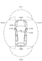
- FIG. 4 is an explanatory diagram showing an example of installation positions of an outside information detection unit and an imaging unit;
- FIG. 1 and 2 are diagrams showing configuration examples of an embodiment of a semiconductor device to which the present technology is applied.
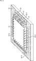
- 1 is a diagram of the semiconductor device 11 viewed from above
- FIG. 2 is a diagram of the semiconductor device 11 viewed obliquely from above.
- the semiconductor device 11 is composed of a wiring board 21 and a chip 22 .
- a chip 22 is arranged on a wiring board 21 that constitutes the semiconductor device 11 .
- a plurality of wirings are connected to the wiring board 21 and the chip 22 .
- the wiring is a bonding wire.
- Chip 22 is electrically connected to wiring board 21 by a plurality of bonding wires 31 .
- the bonding wires 31 include bonding wires for outputting signals and the like processed by the chip 22 to a subsequent control unit provided on the wiring board 21, bonding wires for supplying power supply voltage, and bonding wires for grounding. Including wires.
- the bonding wires 31 are provided on four sides of the chip 22 .
- a solder resist film 34 functioning as an insulating film is formed on the surface of the wiring board 21 .
- Bonding wires 31 are connected to openings 32 - 1 to 32 - 4 and opening 33 provided in a part of the solder resist film 34 .
- the opening 32-1 is formed on the right side of the chip 22 in the drawing
- the opening 32-2 is formed on the lower side of the chip 22 in the drawing
- the opening 32-3 is: It is formed on the left side of the chip 22 in the drawing
- the opening 32-4 is formed on the upper side of the chip 22 in the drawing.
- An opening 33 is also formed on the right side of the chip 22 in the drawing so as to be aligned with the opening 32-1.
- openings 32-1 to 32-4 are simply referred to as openings 32 when there is no need to distinguish them individually. Other parts are similarly described.
- An opening 32 and an opening 33 are formed on the right side of the chip 22, and bonding wires 31 are connected to the respective openings.
- the bonding wire 31 connected to the opening 32 is a low-potential terminal
- the bonding wire 31 connected to the opening 33 is a high-potential terminal. can be allocated.
- low-potential terminal and high-potential terminal are described, but it means a terminal with a high potential difference with respect to a low-potential terminal, and is a relative potential.
- low-potential terminal when one side is set to a low potential, if the potential is high with respect to the low potential, it is described as a high potential. Described as low potential.
- the opening 33 is formed only on the right side of the chip 22, but it can also be formed on other sides. That is, the opening 33 may be formed on at least one side of the right side, the bottom side, the left side, and the top side, and may be formed on two sides, three sides, and four sides, respectively.
- FIG. 3 is a diagram showing a configuration example of the openings 32a and 33a in the first embodiment. 3 and subsequent drawings will be described with reference to enlarged views of the regions where the openings 32a and 33a of the wiring board 21a are arranged.
- the opening 32a is provided in an open state from the position P1 to the position P2 of the solder resist film 34 applied on the wiring board 21a.
- the opening 32a is a region where the solder resist film 34 is not formed.
- the opening 33a is provided in an open state from position P3 to position P5. Positions P1 to P5 are assumed to be in order of position P1, position P2, position P3, position P4, and position P5 from the side closer to the center of the wiring board 21a.
- Terminals 42a-1 to 42a-7 are arranged in the opening 32a.
- Each of the terminals 42a-1 to 42a-7 has a shape in which a lead wire is formed in a rectangular portion.
- the terminals 42a-1 to 42a-7 arranged in the opening 32a are arranged so that the positions of the lead wires (the direction of the lead wires) are staggered.
- the terminal 42a-1 has a lead wire on the position P1 side, and the terminal 42a-2 next to the terminal 42a-1 has a lead wire on the position P2 side.
- the lead wire of the terminal 42a-3 next to the terminal 42a-2 is on the position P1 side. In this way, the terminals 42a are arranged such that the lead wires of the terminals 42a are oriented in different directions between adjacent terminals.
- Terminals 43a-1 to 43a-3 are arranged in the opening 33a.
- the terminals 43a-1 to 43a-3 are also shaped to have lead wires.
- a lead wire of the terminal 43a is provided on the position P5 side.
- a bonding wire 31 set to a low potential is connected to the terminal 42a arranged in the opening 32a, and a bonding wire 31 set to a high potential is connected to the terminal 43a arranged in the opening 33a.
- a terminal to which the low-potential bonding wire 31 is connected and a terminal to which the high-potential bonding wire 31 is connected are located close to each other, they may adversely affect each other. Therefore, normally, a low potential terminal and a high potential terminal (a low potential terminal and a terminal having a high potential difference with respect to the low potential terminal) are arranged apart from each other by a predetermined distance so as not to be affected. However, it is necessary to separate terminals having a potential difference from each other by a predetermined distance, that is, to keep the distance between the terminals long. Downsizing could be difficult.
- the size will likely increase. If the number of terminals increases and the distance between terminals is increased, the size will likely increase. If the size is not increased, there is a possibility that the required terminals cannot be arranged.
- the openings 32a and 33a are provided to separate the low-potential terminals from the high-potential terminals, thereby increasing the distance between the terminals that is not affected by the potential difference. can be secured. Therefore, the wiring board 21a and the chip 22 can be miniaturized, and the semiconductor device 11 can be miniaturized. Even if the number of terminals increases, the size can be reduced while the terminals are arranged so as not to be affected by the potential difference.
- the configuration shown in FIG. 3 is a configuration that can reduce the risk of ion migration.
- Ion migration is, for example, when a wiring board is installed in an environment with a lot of water (humidity), when a voltage is applied, the metal of the anode of the wiring pattern is ionized and moves to the opposite cathode, and then again to the cathode. It is a phenomenon that is generated as a metal in If the metal generated at the cathode grows, it may cause poor insulation and short circuit between the wiring patterns.
- the terminals 42a and 43a respectively arranged in the openings 32a and 33a Since there is a potential difference between the terminals 42a and 43a respectively arranged in the openings 32a and 33a, the terminals correspond to the above-described anode and cathode, and ion migration may occur.
- a distance L is provided from the position P3 of the opening 33a to the position P4 of the tip of the terminal 43a.
- a terminal 42a-2 and a terminal 43a-1 are arranged on the straight line A shown in FIG.
- the tip of the lead wire of terminal 42a-2 is positioned at position P2.
- a solder resist film 34 is formed from position P2 to position P3.
- a distance L is the distance from the position P3 to the position P4 of the tip of the terminal 43a-1.
- the terminals 42a-2 and 43a-1 are not arranged directly across the solder-resist film 34 at a straight line distance, but in the middle of the opening of the solder-resist film 34, in this case, the position of the opening 33a. It is configured to provide an opening from P3 to position P4.
- the unit of distance L is [um]
- the unit of potential difference V is [V].
- the potential difference V is the difference between the potential applied to the terminal 42a-2 and the potential applied to the terminal 43a-1.
- the coefficient a can take a value of 15 to 20 as an example.
- the distance L may be a value larger than the value obtained by multiplying the potential difference V to the power of (1/2) by the coefficient a, as shown in equation (1).
- the wiring board 21a of the first embodiment it is possible to prevent the occurrence of ion migration by preventing an influence between a low potential terminal and a high potential difference terminal. Also, the wiring substrate 21a and the chip 22 can be miniaturized, and the semiconductor device 11 including them can also be miniaturized.
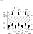
- FIG. 4 is a diagram showing a configuration example of the openings 32 and 33 in the second embodiment.
- the opening 32b and the terminals 42b-1 to 42b-7 formed in the opening 32b are identical to the opening 32a and the terminal 42a-1 formed in the opening 32a in the first embodiment shown in FIG. 42a-7 have the same configuration.
- the terminals 42b-1 to 42b-7 are arranged in the opening 32b so that the lead lines are staggered.
- the opening 32b shown in FIG. 4 is composed of an opening 32b-1, an opening 32b-2, and an opening 32b-3. 43b-3 are arranged. In the configuration example shown in FIG. 4, one opening 32b is formed for one terminal 43b.
- the terminals 42b-2 and 43b-1 are arranged at positions separated by the distance L, for example. That is, instead of arranging the solder resist film 34 directly with a straight line distance, an opening in the solder resist film 34, in this case, an opening from the position P3 to the position P4 of the opening 33b is provided in the middle. ing.
- the terminals 42b-4 and 43b-2, and the terminals 42b-6 and 43b-3 are also arranged at positions separated by a distance L, respectively.
- the terminals that are close to each other in the linear distance are not directly arranged via the solder resist film 34 in the linear distance, but are arranged in the middle.
- An opening of the solder resist film 34 is provided in the .
- the wiring substrate 21b in the second embodiment it is possible to prevent an influence between a low potential terminal and a terminal having a high potential difference with respect to the low potential terminal, and suppress the occurrence of ion migration.
- the wiring substrate 21b and the chip 22 can be miniaturized, and the semiconductor device 11 including them can also be miniaturized.
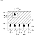
- FIG. 5 is a diagram showing a configuration example of the openings 32 and 33 in the third embodiment.
- the opening 32c and the terminals 42c-1 to 42c-7 formed in the opening 32c are different from the terminal 42a in the first embodiment and the terminal 42a in the second embodiment in that the lead wires are arranged in the same direction. terminal 42b in the form of .
- the lead wire is arranged at the position P12 on the side where the opening 33c is formed in the opening 32c opened from the position P11 to the position P12.
- the direction of arrangement of the lead wires of the plurality of terminals 42c arranged in the opening 32c may be the same direction.
- Terminals 43c may be provided by the number of bonding wires 31 set to a high potential. As shown in FIG. 5, if one bonding wire 31 is set to a high potential, one terminal 43c and an opening 33c may be formed.
- a large opening 32c is formed and a plurality of terminals 43c are arranged as shown in FIG. It can also be configured as By combining the third embodiment shown in FIG. 5 and the second embodiment shown in FIG. 4, as shown in FIG. may be arranged.
- the terminals 42c-2 and 43c are arranged at positions separated by the distance L.
- the distance L is the distance from the position P13 to the position P14 of the opening 33c.
- the opening of the solder-resist film 34 in this case, the opening 33c from the position P13 to the position P14 is not arranged directly through the solder-resist film 34 at a straight line distance. It is configured to have an opening.
- the wiring board 21c In the wiring board 21c according to the third embodiment as well, it is possible to prevent an influence between a low potential terminal and a terminal having a high potential difference with respect to the low potential terminal, thereby suppressing the occurrence of ion migration. . Also, the wiring substrate 21c and the chip 22 can be miniaturized, and the semiconductor device 11 including them can also be miniaturized.
- FIG. 6 is a diagram showing a configuration example of the openings 32 and 33 in the fourth embodiment.
- the opening 32d and the terminals 42d-1 to 42d-7 formed in the opening 32d are similar to the terminal 42c in the third embodiment in that the lead wires are arranged in the same direction. , the orientation is different.
- the terminal 42d in the fourth embodiment has an opening 32d that extends from position P21 to position P23. there is
- the lead wires of the plurality of terminals 42d arranged in the opening 32d may be arranged in the same direction.
- terminals 42d-2 and 43d are arranged at positions separated by the distance L.
- a terminal 42d-2 and a terminal 43d are arranged on the straight line A shown in FIG.
- the tip of the lead wire of the terminal 42d-2 is located at position P21, and the tip opposite to the lead wire is located at position P22.
- a distance L is defined as the distance from the position P22 of the tip of the terminal 43d-1 to the position P23.
- a solder resist film 34 is formed from position P22 to position P23.
- the opening 33d is opened from the position P24 to the position P25, and the terminal 43d is arranged in the opened area.
- the tip of the terminal 43d is positioned at the position P24, and the tip of the lead wire of the terminal 43d is positioned at the position P25.
- the opening 33d and the terminal 43d are formed to have sizes that match the width of the opening 33d and the length of the terminal 43d.
- the distance L is provided on the opening 32d side.
- the terminals 42d-2 and 43d are separated by a distance It is located at a distance of L.
- the terminal 42d-2 and the terminal 43d are not arranged directly across the solder-resist film 34 at a straight line distance, but are separated from the opening of the solder-resist film 34, in this case, from the position P22 of the opening 32d. It is configured such that an opening is provided up to the position P23.
- the wiring substrate 21d in the fourth embodiment it is possible to prevent an influence between a low potential terminal and a high potential difference terminal, and suppress ion migration.
- the wiring board 21d and the chip 22 can be miniaturized, and the semiconductor device 11 including them can also be miniaturized.
- FIG. 7 is a diagram showing a configuration example of the openings 32 and 33 in the fifth embodiment.
- the openings 32e and the terminals 42e-1 to 42e-7 formed in the openings 32e are arranged so that the lead wires are staggered.
- the terminals 42e-2 and 43e are arranged at positions separated by the distance L, for example.
- a terminal 42e-2 and a terminal 43e are arranged on the straight line A shown in FIG.
- the tip of the lead wire of the terminal 42e-2 is positioned at position P31, and the tip opposite to the lead wire is positioned at position P32.
- the distance from the position P32 of the tip of the terminal 42e-2 to the position P33 is the distance L1.
- a solder resist film 34 is formed from position P33 to position P34.
- the opening 33e is open from position P34 to position P36.
- the tip of the terminal 43e is positioned at a position P35, and the tip of the lead wire of the terminal 43e is positioned at a position P36.
- the distance from the position P35 of the tip of the terminal 43e to the position P34 is the distance L2.
- the distance L1 is provided on the side of the opening 32e, and the distance L2 is provided on the side of the opening 33e.
- the distance L is also provided in the example shown in FIG.
- the terminals 42e-2 and 43d are They are arranged at positions separated by a distance L.
- the terminals 42e-2 and 43e are not arranged directly across the solder-resist film 34 at a straight line distance, but are separated from the opening of the solder-resist film 34, in this case, from the position P32 of the opening 32e. It is configured to have an opening that is the sum of the opening up to the position P33 and the opening from the position P34 to the position P35 of the opening 33e.
- the wiring board 21e In the wiring board 21e according to the fifth embodiment as well, it is possible to prevent an influence between a low potential terminal and a terminal having a high potential difference with respect to the low potential terminal, thereby suppressing the occurrence of ion migration. . Also, the wiring board 21e and the chip 22 can be miniaturized, and the semiconductor device 11 including them can also be miniaturized.
- FIG. 8 is a diagram showing a configuration example of the openings 32 and 33 in the sixth embodiment.
- terminals 42 and 43 in the first to fifth embodiments have been described as examples of terminals with lead wires, terminals without lead wires are applied to the present embodiment. You can also In the example shown in FIG. 8, the terminal 43f is a terminal without a lead wire.
- the terminal 43f is formed in a rectangular shape in the central portion of the opening 33f.
- the terminal 43f has no portion in contact with the solder-resist film 34, and the solder-resist film 34 is entirely open around the terminal 43f.
- Such terminals 43f can be applied to the terminals 43 in the first to fifth embodiments.
- terminals 42f-1 to 42f-7 arranged in the opening 32f are illustrated as terminals in which lead wires are formed. 42f-7 may also have a configuration similar to that of terminal 43f. Also, the terminal 42 in the first to fifth embodiments may have a shape without a lead-out line, like the terminal 43f.
- the semiconductor device 11 having any one of the wiring substrates 21 in the first to eighth embodiments can be applied to an imaging element.
- the semiconductor device 11 is composed of a wiring board 21 and a chip 22 .
- a chip 22 is arranged on a wiring board 21 that constitutes the semiconductor device 11 .
- the semiconductor device 11 can be used as an imaging device.
- the image sensor 22 can be a CMOS (Complementary Metal Oxide Semiconductor) image sensor or a CCD (Charge Coupled Device) image sensor.
- the semiconductor device 11 including the image sensor 22 can also be configured as a semiconductor package (PKG).
- FIG. 9 is a cross-sectional view showing a configuration example of a semiconductor package 101 having a hollow structure.
- the image sensor 22 arranged on the wiring board 21 is positioned to be included in the spacer 111 .
- a semiconductor device 11 including a wiring board 21 and an image sensor 22 is a semiconductor device 11 to which any one of the first to eighth embodiments is applied.
- the spacer 111 is arranged on the wiring board 21 .
- a cover glass 113 is fixed onto the spacer 111 via an adhesive 112 .
- Image sensor 22 is arranged in a space surrounded by wiring board 21 , spacer 111 , and cover glass 113 .
- a solder ball 114 is formed on the lower portion of the wiring board 21 .
- the solder balls 114 are connected to the image sensor 22 via bonding wires 31 .
- the solder balls 114 are used when connecting to a substrate (not shown) or the like.
- the present technology can be applied to an imaging device, and can also be applied to cases where the imaging device is configured as a semiconductor package.
- Organic substrates are sometimes used in semiconductor packages, but organic substrates can cause ion migration, and if no countermeasures are taken, ion migration may occur and malfunction may occur. .
- FIG. 9 shows the case where this technology is applied to a semiconductor package having a hollow structure
- this technology can also be applied to a resin-sealed semiconductor package.
- FIG. 10 is a diagram showing a configuration example when the present technology is applied to a resin-sealed semiconductor package.
- the semiconductor package 131 shown in FIG. 10 differs from the semiconductor package 101 shown in FIG. Other points are configured similarly.
- a semiconductor package using an organic substrate on which a chip with a high potential difference is mounted can satisfy the required quality.
- a semiconductor package mounted on a vehicle tends to have a large number of terminals arranged with terminals with a high potential difference, and the environment in which the semiconductor package is used may become hot and humid.
- a semiconductor package including the semiconductor device 11 to which the present technology is applied can satisfy the quality required for such a semiconductor package mounted on a vehicle.
- the size of the semiconductor device 11 can be reduced.
- the size of the semiconductor package including the semiconductor device 11 can also be reduced.
- the technology (the present technology) according to the present disclosure can be applied to various products.
- the technology according to the present disclosure is implemented as a device mounted on any type of moving object such as automobiles, electric vehicles, hybrid electric vehicles, motorcycles, bicycles, personal mobility, airplanes, drones, ships, and robots. may
- FIG. 11 is a block diagram showing a schematic configuration example of a vehicle control system, which is an example of a mobile control system to which the technology according to the present disclosure can be applied.
- a vehicle control system 12000 includes a plurality of electronic control units connected via a communication network 12001.
- the vehicle control system 12000 includes a drive system control unit 12010, a body system control unit 12020, an exterior information detection unit 12030, an interior information detection unit 12040, and an integrated control unit 12050.
- a microcomputer 12051, an audio/image output unit 12052, and an in-vehicle network I/F (Interface) 12053 are illustrated.
- the drive system control unit 12010 controls the operation of devices related to the drive system of the vehicle according to various programs.
- the driving system control unit 12010 includes a driving force generator for generating driving force of the vehicle such as an internal combustion engine or a driving motor, a driving force transmission mechanism for transmitting the driving force to the wheels, and a steering angle of the vehicle. It functions as a control device such as a steering mechanism to adjust and a brake device to generate braking force of the vehicle.
- the body system control unit 12020 controls the operation of various devices equipped on the vehicle body according to various programs.
- the body system control unit 12020 functions as a keyless entry system, a smart key system, a power window device, or a control device for various lamps such as headlamps, back lamps, brake lamps, winkers or fog lamps.
- the body system control unit 12020 can receive radio waves transmitted from a portable device that substitutes for a key or signals from various switches.
- the body system control unit 12020 receives the input of these radio waves or signals and controls the door lock device, power window device, lamps, etc. of the vehicle.
- the vehicle exterior information detection unit 12030 detects information outside the vehicle in which the vehicle control system 12000 is installed.
- the vehicle exterior information detection unit 12030 is connected with an imaging unit 12031 .
- the vehicle exterior information detection unit 12030 causes the imaging unit 12031 to capture an image of the exterior of the vehicle, and receives the captured image.
- the vehicle exterior information detection unit 12030 may perform object detection processing or distance detection processing such as people, vehicles, obstacles, signs, or characters on the road surface based on the received image.
- the imaging unit 12031 is an optical sensor that receives light and outputs an electrical signal according to the amount of received light.
- the imaging unit 12031 can output the electric signal as an image, and can also output it as distance measurement information.
- the light received by the imaging unit 12031 may be visible light or non-visible light such as infrared rays.
- the in-vehicle information detection unit 12040 detects in-vehicle information.
- the in-vehicle information detection unit 12040 is connected to, for example, a driver state detection section 12041 that detects the state of the driver.
- the driver state detection unit 12041 includes, for example, a camera that captures an image of the driver, and the in-vehicle information detection unit 12040 detects the degree of fatigue or concentration of the driver based on the detection information input from the driver state detection unit 12041. It may be calculated, or it may be determined whether the driver is dozing off.
- the microcomputer 12051 calculates control target values for the driving force generator, the steering mechanism, or the braking device based on the information inside and outside the vehicle acquired by the vehicle exterior information detection unit 12030 or the vehicle interior information detection unit 12040, and controls the drive system control unit.
- a control command can be output to 12010 .
- the microcomputer 12051 realizes the functions of ADAS (Advanced Driver Assistance System) including collision avoidance or shock mitigation, follow-up driving based on inter-vehicle distance, vehicle speed maintenance driving, vehicle collision warning, or vehicle lane deviation warning. Cooperative control can be performed for the purpose of ADAS (Advanced Driver Assistance System) including collision avoidance or shock mitigation, follow-up driving based on inter-vehicle distance, vehicle speed maintenance driving, vehicle collision warning, or vehicle lane deviation warning. Cooperative control can be performed for the purpose of ADAS (Advanced Driver Assistance System) including collision avoidance or shock mitigation, follow-up driving based on inter-vehicle distance, vehicle speed maintenance driving, vehicle collision warning, or vehicle
- the microcomputer 12051 controls the driving force generator, the steering mechanism, the braking device, etc. based on the information about the vehicle surroundings acquired by the vehicle exterior information detection unit 12030 or the vehicle interior information detection unit 12040, so that the driver's Cooperative control can be performed for the purpose of autonomous driving, etc., in which vehicles autonomously travel without depending on operation.
- the microcomputer 12051 can output a control command to the body system control unit 12030 based on the information outside the vehicle acquired by the information detection unit 12030 outside the vehicle.
- the microcomputer 12051 controls the headlamps according to the position of the preceding vehicle or the oncoming vehicle detected by the vehicle exterior information detection unit 12030, and performs cooperative control aimed at anti-glare such as switching from high beam to low beam. It can be carried out.
- the audio/image output unit 12052 transmits at least one of audio and/or image output signals to an output device capable of visually or audibly notifying the passengers of the vehicle or the outside of the vehicle.
- an audio speaker 12061 a display unit 12062, and an instrument panel 12063 are illustrated as output devices.
- the display unit 12062 may include at least one of an on-board display and a head-up display, for example.
- FIG. 12 is a diagram showing an example of the installation position of the imaging unit 12031.
- the imaging unit 12031 has imaging units 12101, 12102, 12103, 12104, and 12105.
- the imaging units 12101, 12102, 12103, 12104, and 12105 are provided at positions such as the front nose, side mirrors, rear bumper, back door, and windshield of the vehicle 12100, for example.
- An image pickup unit 12101 provided in the front nose and an image pickup unit 12105 provided above the windshield in the passenger compartment mainly acquire images in front of the vehicle 12100 .
- Imaging units 12102 and 12103 provided in the side mirrors mainly acquire side images of the vehicle 12100 .
- An imaging unit 12104 provided in the rear bumper or back door mainly acquires an image behind the vehicle 12100 .
- the imaging unit 12105 provided above the windshield in the passenger compartment is mainly used for detecting preceding vehicles, pedestrians, obstacles, traffic lights, traffic signs, lanes, and the like.
- FIG. 12 shows an example of the imaging range of the imaging units 12101 to 12104.
- the imaging range 12111 indicates the imaging range of the imaging unit 12101 provided in the front nose
- the imaging ranges 12112 and 12113 indicate the imaging ranges of the imaging units 12102 and 12103 provided in the side mirrors, respectively
- the imaging range 12114 The imaging range of an imaging unit 12104 provided on the rear bumper or back door is shown. For example, by superimposing the image data captured by the imaging units 12101 to 12104, a bird's-eye view image of the vehicle 12100 viewed from above can be obtained.
- At least one of the imaging units 12101 to 12104 may have a function of acquiring distance information.
- at least one of the imaging units 12101 to 12104 may be a stereo camera composed of a plurality of imaging elements, or may be an imaging element having pixels for phase difference detection.
- the microcomputer 12051 determines the distance to each three-dimensional object within the imaging ranges 12111 to 12114 and changes in this distance over time (relative velocity with respect to the vehicle 12100). , it is possible to extract, as the preceding vehicle, the closest three-dimensional object on the traveling path of the vehicle 12100, which runs at a predetermined speed (for example, 0 km/h or more) in substantially the same direction as the vehicle 12100. can. Furthermore, the microcomputer 12051 can set the inter-vehicle distance to be secured in advance in front of the preceding vehicle, and perform automatic brake control (including following stop control) and automatic acceleration control (including following start control). In this way, cooperative control can be performed for the purpose of automatic driving in which the vehicle runs autonomously without relying on the operation of the driver.
- automatic brake control including following stop control
- automatic acceleration control including following start control
- the microcomputer 12051 converts three-dimensional object data related to three-dimensional objects to other three-dimensional objects such as motorcycles, ordinary vehicles, large vehicles, pedestrians, and utility poles. It can be classified and extracted and used for automatic avoidance of obstacles. For example, the microcomputer 12051 distinguishes obstacles around the vehicle 12100 into those that are visible to the driver of the vehicle 12100 and those that are difficult to see. Then, the microcomputer 12051 judges the collision risk indicating the degree of danger of collision with each obstacle, and when the collision risk is equal to or higher than the set value and there is a possibility of collision, the collision is possible via the audio speaker 12061 and the display unit 12062. By outputting an alarm to the driver via the drive system control unit 12010 and performing forced deceleration and avoidance steering via the drive system control unit 12010, driving support for collision avoidance can be performed.
- At least one of the imaging units 12101 to 12104 may be an infrared camera that detects infrared rays.
- the microcomputer 12051 can recognize a pedestrian by determining whether or not the pedestrian exists in the captured images of the imaging units 12101 to 12104 .
- recognition of a pedestrian is performed by, for example, a procedure for extracting feature points in images captured by the imaging units 12101 to 12104 as infrared cameras, and performing pattern matching processing on a series of feature points indicating the outline of an object to determine whether or not the pedestrian is a pedestrian.
- the audio image output unit 12052 outputs a rectangular outline for emphasis to the recognized pedestrian. is superimposed on the display unit 12062 . Also, the audio/image output unit 12052 may control the display unit 12062 to display an icon or the like indicating a pedestrian at a desired position.
- the present technology can also take the following configuration.
- a chip a wiring board; a wire connecting the chip and the wiring substrate, A semiconductor device, wherein a first opening and a second opening to which the wire is connected are formed in at least one side of the wiring substrate, which is a surface of the wiring substrate on which an insulating film is formed.
- a first terminal formed in the first opening and a second terminal formed in the second opening are arranged at positions separated by a predetermined distance in the opening.
- the semiconductor device according to (1) On a straight line on which the first terminal and the second terminal are arranged, the distance between the first terminal and the second terminal is the distance between the first terminal and the second terminal.
- the semiconductor device according to (2) which is separated by the predetermined distance except for the distance of the insulating film therebetween.
- the wire set to a low potential is connected to the first terminal, and the wire set to a high potential with respect to the low potential is connected to the second terminal.
- the semiconductor device according to (5), wherein the coefficient is 15 to 20.
- the semiconductor device according to any one of (2) to (6), wherein the predetermined distance is provided within the first opening.
- the predetermined distance is a distance obtained by adding a first distance provided in the first opening and a second distance provided in the second opening.
- the semiconductor device according to any one of 6).
- the first terminal has a lead wire, and is arranged in the first opening so that the lead wire is oriented in the direction in which the second opening is positioned.
- the semiconductor device according to any one of 9).
- the first terminal has a lead wire, and is arranged in the first opening such that the direction of the lead wire is opposite to the direction of the second opening.
- (13) The semiconductor device according to any one of (2) to (12), wherein one second terminal is formed in the second opening.
- (15) The semiconductor device according to any one of (1) to (14), wherein the chip is an image sensor.
- the imaging device according to (16) above which is a semiconductor package with a hollow structure.
Landscapes
- Engineering & Computer Science (AREA)
- Multimedia (AREA)
- Signal Processing (AREA)
- Wire Bonding (AREA)
- Physics & Mathematics (AREA)
- Geometry (AREA)
- Solid State Image Pick-Up Elements (AREA)
Abstract
Description
図1、図2は、本技術を適用した半導体装置の一実施の形態の構成例を示す図である。図1は、半導体装置11を上側からみたときの図であり、図2は、半導体装置11を斜め上側から見たときの図である。
以下に、開口部32と開口部33の構成について説明を加える。図3は、第1の実施の形態における開口部32a、開口部33aの構成例を示す図である。図3以降の説明においては、配線基板21aの開口部32aと開口部33aが配置されている領域を拡大した図を示し、説明を行う。
距離L≧係数a×電位差V^(1/2) ・・・(1)
図4は、開口部32、開口部33の第2の実施の形態における構成例を示す図である。
図5は、開口部32、開口部33の第3の実施の形態における構成例を示す図である。
図6は、開口部32、開口部33の第4の実施の形態における構成例を示す図である。
図7は、開口部32、開口部33の第5の実施の形態における構成例を示す図である。
図8は、開口部32、開口部33の第6の実施の形態における構成例を示す図である。
第1乃至第8の実施の形態における配線基板21のいずれかを有する半導体装置11は、撮像素子に適用できる。
本開示に係る技術(本技術)は、様々な製品へ応用することができる。例えば、本開示に係る技術は、自動車、電気自動車、ハイブリッド電気自動車、自動二輪車、自転車、パーソナルモビリティ、飛行機、ドローン、船舶、ロボット等のいずれかの種類の移動体に搭載される装置として実現されてもよい。
(1)
チップと、
配線基板と、
前記チップと前記配線基板を接続するワイヤと
を備え、
前記配線基板の絶縁膜が形成されている面であり、前記配線基板の少なくとも一辺に、前記ワイヤが接続される第1の開口部と第2の開口部が形成されている
半導体装置。
(2)
前記第1の開口部に形成されている第1の端子と、前記第2の開口部に形成されている第2の端子は、開口部において所定の距離だけ離れた位置に配置されている
前記(1)に記載の半導体装置。
(3)
前記第1の端子と前記第2の端子が配置されている直線上において、前記第1の端子と前記第2の端子の間の距離は、前記第1の端子と前記第2の端子との間にある前記絶縁膜の距離を除いて、前記所定の距離だけ離れている
前記(2)に記載の半導体装置。
(4)
前記第1の端子には、低電位に設定されている前記ワイヤが接続され、前記第2の端子には、前記低電位に対して高電位に設定されている前記ワイヤが接続されている
前記(2)または(3)に記載の半導体装置。
(5)
前記所定の距離は、前記低電位と前記高電位の電位差を用いて次式により表される
距離=係数×電位差^(1/2)
前記(4)に記載の半導体装置。
(6)
前記係数は、15乃至20である
前記(5)に記載の半導体装置。
(7)
前記所定の距離は、前記第2の開口部内に設けられている
前記(2)乃至(6)のいずれかに記載の半導体装置。
(8)
前記所定の距離は、前記第1の開口部内に設けられている
前記(2)乃至(6)のいずれかに記載の半導体装置。
(9)
前記所定の距離は、前記第1の開口部に設けられている第1の距離と、前記第2の開口部内に設けられている第2の距離を加算した距離である
前記(2)乃至(6)のいずれかに記載の半導体装置。
(10)
前記第1の端子は、引き出し線を有し、前記引き出し線の向きが互い違いになるように前記第1の開口部内に配置されている
前記(2)乃至(9)のいずれかに記載の半導体装置。
(11)
前記第1の端子は、引き出し線を有し、前記引き出し線の向きが前記第2の開口部が位置する方向になるように前記第1の開口部内に配置されている
前記(2)乃至(9)のいずれかに記載の半導体装置。
(12)
前記第1の端子は、引き出し線を有し、前記引き出し線の向きが前記第2の開口部がある方向と逆側になるように前記第1の開口部内に配置されている
前記(2)乃至(9)のいずれかに記載の半導体装置。
(13)
前記第2の端子は、前記第2の開口部内に1つ形成されている
前記(2)乃至(12)のいずれかに記載の半導体装置。
(14)
前記第2の端子は、前記第2の開口部内に複数形成されている
前記(2)乃至(12)のいずれかに記載の半導体装置。
(15)
前記チップは、イメージセンサである
前記(1)乃至(14)のいずれかに記載の半導体装置。
(16)
イメージセンサのチップと、
配線基板と、
前記チップと前記配線基板を接続するワイヤと
を備え、
前記配線基板の絶縁膜が形成されている面であり、前記配線基板の少なくとも一辺に、前記ワイヤが接続される開口部が少なくとも2箇所形成されている
撮像装置。
(17)
中空構造の半導体パッケージである
前記(16)に記載の撮像装置。
(18)
前記チップが樹脂封止されている半導体パッケージである
前記(16)に記載の撮像装置。
Claims (18)
- チップと、
配線基板と、
前記チップと前記配線基板を接続するワイヤと
を備え、
前記配線基板の絶縁膜が形成されている面であり、前記配線基板の少なくとも一辺に、前記ワイヤが接続される第1の開口部と第2の開口部が形成されている
半導体装置。 - 前記第1の開口部に形成されている第1の端子と、前記第2の開口部に形成されている第2の端子は、開口部において所定の距離だけ離れた位置に配置されている
請求項1に記載の半導体装置。 - 前記第1の端子と前記第2の端子が配置されている直線上において、前記第1の端子と前記第2の端子の間の距離は、前記第1の端子と前記第2の端子との間にある前記絶縁膜の距離を除いて、前記所定の距離だけ離れている
請求項2に記載の半導体装置。 - 前記第1の端子には、低電位に設定されている前記ワイヤが接続され、前記第2の端子には、前記低電位に対して高電位に設定されている前記ワイヤが接続されている
請求項2に記載の半導体装置。 - 前記所定の距離は、前記低電位と前記高電位の電位差を用いて次式により表される
距離=係数×電位差^(1/2)
請求項4に記載の半導体装置。 - 前記係数は、15乃至20である
請求項5に記載の半導体装置。 - 前記所定の距離は、前記第2の開口部内に設けられている
請求項2に記載の半導体装置。 - 前記所定の距離は、前記第1の開口部内に設けられている
請求項2に記載の半導体装置。 - 前記所定の距離は、前記第1の開口部に設けられている第1の距離と、前記第2の開口部内に設けられている第2の距離を加算した距離である
請求項2に記載の半導体装置。 - 前記第1の端子は、引き出し線を有し、前記引き出し線の向きが互い違いになるように前記第1の開口部内に配置されている
請求項2に記載の半導体装置。 - 前記第1の端子は、引き出し線を有し、前記引き出し線の向きが前記第2の開口部が位置する方向になるように前記第1の開口部内に配置されている
請求項2に記載の半導体装置。 - 前記第1の端子は、引き出し線を有し、前記引き出し線の向きが前記第2の開口部がある方向と逆側になるように前記第1の開口部内に配置されている
請求項2に記載の半導体装置。 - 前記第2の端子は、前記第2の開口部内に1つ形成されている
請求項2に記載の半導体装置。 - 前記第2の端子は、前記第2の開口部内に複数形成されている
請求項2に記載の半導体装置。 - 前記チップは、イメージセンサである
請求項1に記載の半導体装置。 - イメージセンサのチップと、
配線基板と、
前記チップと前記配線基板を接続するワイヤと
を備え、
前記配線基板の絶縁膜が形成されている面であり、前記配線基板の少なくとも一辺に、前記ワイヤが接続される開口部が少なくとも2箇所形成されている
撮像装置。 - 中空構造の半導体パッケージである
請求項16に記載の撮像装置。 - 前記チップが樹脂封止されている半導体パッケージである
請求項16に記載の撮像装置。
Priority Applications (2)
| Application Number | Priority Date | Filing Date | Title |
|---|---|---|---|
| US18/262,932 US20240088010A1 (en) | 2021-02-05 | 2022-01-05 | Semiconductor device and imaging device |
| KR1020237024769A KR20230141770A (ko) | 2021-02-05 | 2022-01-05 | 반도체 장치, 촬상 장치 |
Applications Claiming Priority (2)
| Application Number | Priority Date | Filing Date | Title |
|---|---|---|---|
| JP2021-017083 | 2021-02-05 | ||
| JP2021017083 | 2021-02-05 |
Publications (1)
| Publication Number | Publication Date |
|---|---|
| WO2022168514A1 true WO2022168514A1 (ja) | 2022-08-11 |
Family
ID=82742206
Family Applications (1)
| Application Number | Title | Priority Date | Filing Date |
|---|---|---|---|
| PCT/JP2022/000076 Ceased WO2022168514A1 (ja) | 2021-02-05 | 2022-01-05 | 半導体装置、撮像装置 |
Country Status (3)
| Country | Link |
|---|---|
| US (1) | US20240088010A1 (ja) |
| KR (1) | KR20230141770A (ja) |
| WO (1) | WO2022168514A1 (ja) |
Citations (5)
| Publication number | Priority date | Publication date | Assignee | Title |
|---|---|---|---|---|
| JPH03220755A (ja) * | 1990-01-26 | 1991-09-27 | Olympus Optical Co Ltd | 半導体装置 |
| JP2007501537A (ja) * | 2003-06-09 | 2007-01-25 | フリースケール セミコンダクター インコーポレイテッド | ワイヤ・ボンドの位置付けを最適化した半導体パッケージ |
| JP2010027856A (ja) * | 2008-07-18 | 2010-02-04 | Panasonic Corp | 半導体装置 |
| JP2011155184A (ja) * | 2010-01-28 | 2011-08-11 | Renesas Electronics Corp | 配線構造 |
| JP2015023159A (ja) * | 2013-07-19 | 2015-02-02 | ルネサスエレクトロニクス株式会社 | 半導体装置およびその製造方法 |
Family Cites Families (1)
| Publication number | Priority date | Publication date | Assignee | Title |
|---|---|---|---|---|
| JPH05308137A (ja) | 1992-04-30 | 1993-11-19 | Sony Corp | 半導体装置 |
-
2022
- 2022-01-05 KR KR1020237024769A patent/KR20230141770A/ko active Pending
- 2022-01-05 WO PCT/JP2022/000076 patent/WO2022168514A1/ja not_active Ceased
- 2022-01-05 US US18/262,932 patent/US20240088010A1/en active Pending
Patent Citations (5)
| Publication number | Priority date | Publication date | Assignee | Title |
|---|---|---|---|---|
| JPH03220755A (ja) * | 1990-01-26 | 1991-09-27 | Olympus Optical Co Ltd | 半導体装置 |
| JP2007501537A (ja) * | 2003-06-09 | 2007-01-25 | フリースケール セミコンダクター インコーポレイテッド | ワイヤ・ボンドの位置付けを最適化した半導体パッケージ |
| JP2010027856A (ja) * | 2008-07-18 | 2010-02-04 | Panasonic Corp | 半導体装置 |
| JP2011155184A (ja) * | 2010-01-28 | 2011-08-11 | Renesas Electronics Corp | 配線構造 |
| JP2015023159A (ja) * | 2013-07-19 | 2015-02-02 | ルネサスエレクトロニクス株式会社 | 半導体装置およびその製造方法 |
Also Published As
| Publication number | Publication date |
|---|---|
| US20240088010A1 (en) | 2024-03-14 |
| KR20230141770A (ko) | 2023-10-10 |
Similar Documents
| Publication | Publication Date | Title |
|---|---|---|
| US12272714B2 (en) | Solid-state imaging device | |
| JP7499242B2 (ja) | 半導体パッケージ、および、電子装置 | |
| WO2018030139A1 (ja) | 撮像素子パッケージおよびカメラモジュール | |
| US11152726B2 (en) | Connector device and connector system | |
| WO2022158278A1 (ja) | 撮像素子、撮像装置 | |
| US11670625B2 (en) | Imaging unit having a stacked structure and electronic apparatus including the imaging unit | |
| JP7462620B2 (ja) | 半導体パッケージ、半導体パッケージの製造方法、および、電子装置 | |
| WO2022168514A1 (ja) | 半導体装置、撮像装置 | |
| WO2019176454A1 (ja) | 半導体装置、撮像装置、および電子機器 | |
| WO2023007797A1 (ja) | 固体撮像素子、撮像装置、および電子機器 | |
| CN113661700B (zh) | 成像装置与成像方法 | |
| WO2022259971A1 (ja) | 駆動回路、および、固体撮像素子 | |
| US11722804B2 (en) | Imaging device and imaging system having a stacked structure for pixel portion and signal processing circuit portion | |
| US20250251238A1 (en) | Semiconductor package and module | |
| JP7561733B2 (ja) | 半導体パッケージ、および、半導体パッケージの製造方法 | |
| WO2024224807A1 (ja) | 半導体パッケージ、および、半導体パッケージの製造方法 | |
| JP7624393B2 (ja) | 半導体パッケージ、電子装置、および、半導体パッケージの製造方法 | |
| WO2024075398A1 (ja) | カメラモジュール、および、撮像装置 | |
| WO2024185282A1 (ja) | 半導体パッケージ、半導体装置、および、半導体パッケージの製造方法 | |
| WO2024024278A1 (ja) | パッケージおよびパッケージの製造方法 | |
| WO2025004532A1 (ja) | 異常検出回路、異常検出方法、および撮像システム | |
| WO2024111248A1 (ja) | 半導体パッケージ、光学装置、および、半導体パッケージの製造方法 | |
| WO2026083724A1 (ja) | 光検出装置 |
Legal Events
| Date | Code | Title | Description |
|---|---|---|---|
| 121 | Ep: the epo has been informed by wipo that ep was designated in this application |
Ref document number: 22749393 Country of ref document: EP Kind code of ref document: A1 |
|
| WWE | Wipo information: entry into national phase |
Ref document number: 18262932 Country of ref document: US |
|
| NENP | Non-entry into the national phase |
Ref country code: DE |
|
| 122 | Ep: pct application non-entry in european phase |
Ref document number: 22749393 Country of ref document: EP Kind code of ref document: A1 |
|
| NENP | Non-entry into the national phase |
Ref country code: JP |
|
| WWW | Wipo information: withdrawn in national office |
Ref document number: 1020237024769 Country of ref document: KR |