WO2022163783A1 - 搬送装置、搬送方法、及び半導体装置の製造方法 - Google Patents
搬送装置、搬送方法、及び半導体装置の製造方法 Download PDFInfo
- Publication number
- WO2022163783A1 WO2022163783A1 PCT/JP2022/003187 JP2022003187W WO2022163783A1 WO 2022163783 A1 WO2022163783 A1 WO 2022163783A1 JP 2022003187 W JP2022003187 W JP 2022003187W WO 2022163783 A1 WO2022163783 A1 WO 2022163783A1
- Authority
- WO
- WIPO (PCT)
- Prior art keywords
- substrate
- irradiation
- holding mechanism
- laser beam
- unit
- Prior art date
- Legal status (The legal status is an assumption and is not a legal conclusion. Google has not performed a legal analysis and makes no representation as to the accuracy of the status listed.)
- Ceased
Links
Images


Classifications
-
- H—ELECTRICITY
- H10—SEMICONDUCTOR DEVICES; ELECTRIC SOLID-STATE DEVICES NOT OTHERWISE PROVIDED FOR
- H10P—GENERIC PROCESSES OR APPARATUS FOR THE MANUFACTURE OR TREATMENT OF DEVICES COVERED BY CLASS H10
- H10P72/00—Handling or holding of wafers, substrates or devices during manufacture or treatment thereof
- H10P72/70—Handling or holding of wafers, substrates or devices during manufacture or treatment thereof for supporting or gripping
- H10P72/78—Handling or holding of wafers, substrates or devices during manufacture or treatment thereof for supporting or gripping using vacuum or suction, e.g. Bernoulli chucks
-
- B—PERFORMING OPERATIONS; TRANSPORTING
- B65—CONVEYING; PACKING; STORING; HANDLING THIN OR FILAMENTARY MATERIAL
- B65G—TRANSPORT OR STORAGE DEVICES, e.g. CONVEYORS FOR LOADING OR TIPPING, SHOP CONVEYOR SYSTEMS OR PNEUMATIC TUBE CONVEYORS
- B65G49/00—Conveying systems characterised by their application for specified purposes not otherwise provided for
- B65G49/05—Conveying systems characterised by their application for specified purposes not otherwise provided for for fragile or damageable materials or articles
- B65G49/06—Conveying systems characterised by their application for specified purposes not otherwise provided for for fragile or damageable materials or articles for fragile sheets, e.g. glass
-
- H—ELECTRICITY
- H10—SEMICONDUCTOR DEVICES; ELECTRIC SOLID-STATE DEVICES NOT OTHERWISE PROVIDED FOR
- H10D—INORGANIC ELECTRIC SEMICONDUCTOR DEVICES
- H10D30/00—Field-effect transistors [FET]
- H10D30/01—Manufacture or treatment
- H10D30/021—Manufacture or treatment of FETs having insulated gates [IGFET]
-
- H—ELECTRICITY
- H10—SEMICONDUCTOR DEVICES; ELECTRIC SOLID-STATE DEVICES NOT OTHERWISE PROVIDED FOR
- H10D—INORGANIC ELECTRIC SEMICONDUCTOR DEVICES
- H10D30/00—Field-effect transistors [FET]
- H10D30/60—Insulated-gate field-effect transistors [IGFET]
- H10D30/67—Thin-film transistors [TFT]
-
- H—ELECTRICITY
- H10—SEMICONDUCTOR DEVICES; ELECTRIC SOLID-STATE DEVICES NOT OTHERWISE PROVIDED FOR
- H10P—GENERIC PROCESSES OR APPARATUS FOR THE MANUFACTURE OR TREATMENT OF DEVICES COVERED BY CLASS H10
- H10P14/00—Formation of materials, e.g. in the shape of layers or pillars
- H10P14/20—Formation of materials, e.g. in the shape of layers or pillars of semiconductor materials
- H10P14/38—Formation of materials, e.g. in the shape of layers or pillars of semiconductor materials characterised by treatments done after the formation of the materials
- H10P14/3802—Crystallisation or recrystallisation of non-monocrystalline semiconductor materials, e.g. regrowth
- H10P14/3808—Crystallisation or recrystallisation of non-monocrystalline semiconductor materials, e.g. regrowth using laser beams
-
- H—ELECTRICITY
- H10—SEMICONDUCTOR DEVICES; ELECTRIC SOLID-STATE DEVICES NOT OTHERWISE PROVIDED FOR
- H10P—GENERIC PROCESSES OR APPARATUS FOR THE MANUFACTURE OR TREATMENT OF DEVICES COVERED BY CLASS H10
- H10P34/00—Irradiation with electromagnetic or particle radiation of wafers, substrates or parts of devices
- H10P34/40—Irradiation with electromagnetic or particle radiation of wafers, substrates or parts of devices with high-energy radiation
- H10P34/42—Irradiation with electromagnetic or particle radiation of wafers, substrates or parts of devices with high-energy radiation with electromagnetic radiation, e.g. laser annealing
-
- H—ELECTRICITY
- H10—SEMICONDUCTOR DEVICES; ELECTRIC SOLID-STATE DEVICES NOT OTHERWISE PROVIDED FOR
- H10P—GENERIC PROCESSES OR APPARATUS FOR THE MANUFACTURE OR TREATMENT OF DEVICES COVERED BY CLASS H10
- H10P72/00—Handling or holding of wafers, substrates or devices during manufacture or treatment thereof
- H10P72/04—Apparatus for manufacture or treatment
- H10P72/0431—Apparatus for thermal treatment
- H10P72/0436—Apparatus for thermal treatment mainly by radiation
-
- H—ELECTRICITY
- H10—SEMICONDUCTOR DEVICES; ELECTRIC SOLID-STATE DEVICES NOT OTHERWISE PROVIDED FOR
- H10P—GENERIC PROCESSES OR APPARATUS FOR THE MANUFACTURE OR TREATMENT OF DEVICES COVERED BY CLASS H10
- H10P72/00—Handling or holding of wafers, substrates or devices during manufacture or treatment thereof
- H10P72/30—Handling or holding of wafers, substrates or devices during manufacture or treatment thereof for conveying, e.g. between different workstations
- H10P72/32—Handling or holding of wafers, substrates or devices during manufacture or treatment thereof for conveying, e.g. between different workstations between different workstations
- H10P72/3208—Changing the direction of the conveying path
-
- H—ELECTRICITY
- H10—SEMICONDUCTOR DEVICES; ELECTRIC SOLID-STATE DEVICES NOT OTHERWISE PROVIDED FOR
- H10P—GENERIC PROCESSES OR APPARATUS FOR THE MANUFACTURE OR TREATMENT OF DEVICES COVERED BY CLASS H10
- H10P72/00—Handling or holding of wafers, substrates or devices during manufacture or treatment thereof
- H10P72/30—Handling or holding of wafers, substrates or devices during manufacture or treatment thereof for conveying, e.g. between different workstations
- H10P72/33—Handling or holding of wafers, substrates or devices during manufacture or treatment thereof for conveying, e.g. between different workstations into and out of processing chamber
- H10P72/3314—Continuous loading and unloading into and out of a processing chamber, e.g. transporting belts within processing chambers
-
- H—ELECTRICITY
- H10—SEMICONDUCTOR DEVICES; ELECTRIC SOLID-STATE DEVICES NOT OTHERWISE PROVIDED FOR
- H10P—GENERIC PROCESSES OR APPARATUS FOR THE MANUFACTURE OR TREATMENT OF DEVICES COVERED BY CLASS H10
- H10P72/00—Handling or holding of wafers, substrates or devices during manufacture or treatment thereof
- H10P72/30—Handling or holding of wafers, substrates or devices during manufacture or treatment thereof for conveying, e.g. between different workstations
- H10P72/36—Handling or holding of wafers, substrates or devices during manufacture or treatment thereof for conveying, e.g. between different workstations using air tracks
-
- H—ELECTRICITY
- H10—SEMICONDUCTOR DEVICES; ELECTRIC SOLID-STATE DEVICES NOT OTHERWISE PROVIDED FOR
- H10P—GENERIC PROCESSES OR APPARATUS FOR THE MANUFACTURE OR TREATMENT OF DEVICES COVERED BY CLASS H10
- H10P72/00—Handling or holding of wafers, substrates or devices during manufacture or treatment thereof
- H10P72/70—Handling or holding of wafers, substrates or devices during manufacture or treatment thereof for supporting or gripping
- H10P72/76—Handling or holding of wafers, substrates or devices during manufacture or treatment thereof for supporting or gripping using mechanical means, e.g. clamps or pinches
- H10P72/7604—Handling or holding of wafers, substrates or devices during manufacture or treatment thereof for supporting or gripping using mechanical means, e.g. clamps or pinches the wafers being placed on a susceptor, stage or support
- H10P72/7618—Handling or holding of wafers, substrates or devices during manufacture or treatment thereof for supporting or gripping using mechanical means, e.g. clamps or pinches the wafers being placed on a susceptor, stage or support characterised by a movable susceptor, stage or support, others than those only rotating on their own vertical axis, e.g. susceptors on a rotating carrousel
Definitions
- the present invention relates to a carrier device, a carrier method, and a semiconductor device manufacturing method.
- Patent Document 1 discloses a laser annealing apparatus for forming a polycrystalline silicon thin film.
- a projection lens converges laser light onto a substrate so that the laser light forms a linear irradiation area.
- the amorphous silicon film is crystallized into a polysilicon film.
- the transport unit transports the substrate while the floating unit floats the substrate. Furthermore, in the levitation unit, the loading position and the unloading position of the substrate are common. The transport unit transports the substrate along each side of the levitation unit. By circulating the substrate twice on the floating unit, almost the entire surface of the substrate is irradiated with the laser beam.
- the transport apparatus is a transport apparatus for transporting the substrate in order to irradiate the substrate with a linear laser beam, comprising: a substrate floating unit for floating the substrate on its upper surface; a holding mechanism for holding a substrate; a moving mechanism for moving the holding mechanism in a direction inclined from a direction orthogonal to the line-shaped laser beam in a top view so as to change the irradiation position of the laser beam on the substrate; It has
- the transport device is a transport device for transporting the substrate in order to irradiate the substrate with a line-shaped laser beam, the transport device being arranged below the substrate to float the substrate.
- 1 substrate levitation unit comprising: a first substrate levitation unit arranged from a central portion of the substrate to one end side of the substrate in top view; and a second substrate arranged below the substrate for floating the substrate.
- a second substrate floating unit arranged on the other end side of the substrate from the center portion of the substrate when viewed from the top, and a second substrate floating unit arranged below the center portion of the substrate and sucking the substrate.
- a holding mechanism for holding the substrate, and the holding mechanism is moved along the gap between the first substrate floating unit and the second substrate floating unit to move the substrate with respect to the irradiation position of the laser beam. and a moving mechanism.
- the transport method is a transport method for transporting the substrate in order to irradiate the substrate with a linear laser beam, comprising: (a) a levitation unit arranged below the substrate; (b) holding the substrate by a holding mechanism; and (c) changing the irradiation position of the laser beam with respect to the substrate. and moving the holding mechanism in a direction inclined from a direction perpendicular to the longitudinal direction of the laser beam.
- the transport method is a transport method for transporting the substrate in order to irradiate the substrate with a line-shaped laser beam, comprising: (A) a first laser beam arranged below the substrate; A substrate floating unit is used to float one end side of the substrate from the central portion of the substrate in top view, and a second substrate floating unit arranged below the substrate is used to float the substrate in top view. (B) attracting and holding the substrate using a holding mechanism arranged below the central portion of the substrate; (C) and moving the holding mechanism along the gap between the first substrate floating unit and the second substrate floating unit to move the substrate with respect to the irradiation position of the laser beam.
- a method of manufacturing a semiconductor device includes the steps of (s1) forming an amorphous film on a substrate, and (s2) crystallizing the amorphous film to form a crystallized film. and irradiating the substrate with a line-shaped laser beam to anneal the amorphous film, wherein the step of (s2) annealing includes: (sb) holding the substrate by a holding mechanism; and (sc) changing the irradiation position of the laser beam on the substrate in the longitudinal direction of the line-shaped laser beam in top view. and moving the retaining mechanism in a direction oblique from the orthogonal direction.
- a method of manufacturing a semiconductor device includes the steps of (S1) forming an amorphous film on a substrate, and (S2) crystallizing the amorphous film to form a crystallized film. and irradiating the substrate with a line-shaped laser beam to anneal the amorphous film, wherein the step of (S2) annealing includes (SA) arranged below the substrate.
- SA first substrate floating unit is used to float one end side of the substrate from the central portion of the substrate in top view, and a second substrate floating unit disposed below the substrate is used to float the substrate in top view.
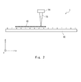
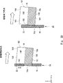
- FIG. 1 is a top view schematically showing a laser irradiation device according to a first embodiment
- FIG. 1 is a side sectional view schematically showing a laser irradiation device according to a first embodiment
- FIG. It is a figure for demonstrating the intensity distribution of a pulsed laser beam.
- It is a top view which shows the irradiation pitch of a pulsed laser beam, and the manufacturing pitch of TFT.
- FIG. 11 is a top view showing the configuration of a conveying device according to a second embodiment; It is a top view for demonstrating the conveyance process in a conveying apparatus.
- FIG. 4 is a schematic diagram showing an exhaust system of the holding mechanism;
- FIG. 4 is a schematic diagram for explaining valve control of the holding mechanism; It is a side view which shows the structure of a conveying apparatus typically.
- FIG. 11 is a top view schematically showing a laser irradiation device according to a third embodiment;
- FIG. 4 is a schematic diagram for explaining adsorption failure due to moment of inertia.
- FIG. 3 is a schematic diagram for explaining adsorption-separation electrification;
- FIG. 4 is a top view for explaining an irradiation process according to Example 1;
- FIG. 10 is a top view for explaining an irradiation process according to Example 2;
- FIG. 11 is a top view for explaining an irradiation process according to Example 3; 1 is a cross-sectional view showing a simplified configuration of an organic EL display; FIG. It is process sectional drawing which shows the manufacturing method of the semiconductor device concerning this Embodiment. It is process sectional drawing which shows the manufacturing method of the semiconductor device concerning this Embodiment.
- FIG. 10 is a top view schematically showing the configuration of Modification 1;
- FIG. 11 is a top view schematically showing the configuration of Modified Example 2;
- FIG. 5 is a top view for explaining the configuration of Irradiation Example 1;
- FIG. 10 is a top view for explaining the configuration of Example 2 of irradiation;
- FIG. 10 is a top view for explaining the configuration of Example 2 of irradiation;
- FIG. 10 is a top view for explaining the configuration of Example 2 of irradiation;
- FIG. 10 is a top view for explaining the configuration of Example 2 of irradiation;
- FIG. 10 is
- FIG. 11 is a top view for explaining the configuration of Example 3 of irradiation;
- FIG. 11 is a top view for explaining the configuration of Example 4 of irradiation;
- FIG. 11 is a top view for explaining the configuration of Example 4 of irradiation;
- FIG. 11 is a top view for explaining the configuration of Example 5 of irradiation;
- FIG. 11 is a top view for explaining the configuration of Example 5 of irradiation;
- FIG. 4 is a top view schematically showing a configuration for simultaneously transporting two substrates;
- FIG. 4 is a top view schematically showing a configuration for simultaneously transporting two substrates;
- FIG. 4 is a top view schematically showing a configuration for simultaneously transporting two substrates;
- FIG. 4 is a top view schematically showing a configuration for simultaneously transporting two substrates;
- FIG. 4 is a top view schematically showing a configuration for simultaneously transporting two substrates;
- a conveying device is used in a laser irradiation device such as a laser annealing device.
- the laser annealing apparatus is, for example, an excimer laser annealing (ELA) apparatus for forming a low temperature poly-silicon (LTPS) film.
- ELA excimer laser annealing
- LTPS low temperature poly-silicon
- FIG. 1 is a top view schematically showing the configuration of a laser irradiation device 1.
- FIG. 2 is a side sectional view schematically showing the configuration of the laser irradiation device 1. As shown in FIG.
- the diagrams shown below show an xyz three-dimensional orthogonal coordinate system as appropriate for simplification of explanation.
- the z direction is the vertical direction
- the y direction is the direction along the line-shaped irradiation area 15a.
- the x-direction is the direction orthogonal to the z-direction and the y-direction. That is, the y direction is the longitudinal direction of the linear irradiation area 15a, and the x direction is the lateral direction perpendicular to the longitudinal direction.
- the laser irradiation device 1 includes a floating unit 10, a transport unit 11, and a laser irradiation section .
- the levitation unit 10 and the transport unit 11 constitute a transport device.
- the levitation unit 10 is configured to eject gas from the surface of the levitation unit 10 .
- the levitation unit 10 levitates the object 16 to be processed on its upper surface.
- the gas ejected from the surface of the floating unit 10 is sprayed onto the lower surface of the object 16 to float, thereby causing the object 16 to float.
- the object 16 to be processed is a glass substrate.
- the floating unit 10 adjusts the floating amount so that the object 16 to be processed does not come into contact with another mechanism (not shown) arranged above the object 16 to be processed.
- the transport unit 11 transports the floating object to be processed 16 in the transport direction.
- the transport unit 11 has a holding mechanism 12 and a moving mechanism 13 .
- the holding mechanism 12 holds the object 16 to be processed.
- the holding mechanism 12 can be configured using a vacuum suction mechanism.
- the vacuum adsorption mechanism is made of metal material such as aluminum alloy.
- the holding mechanism 12 may be made of a resin-based material such as PEEK (polyetheretherketone) material.
- a suction groove, a suction hole, and the like are formed on the upper surface of the holding mechanism 12 .
- the holding mechanism 12 may be made of a porous material.
- the holding mechanism 12 vacuum suction mechanism
- the holding mechanism 12 is connected to an exhaust port (not shown), and the exhaust port is connected to an ejector, a vacuum pump, and the like. Therefore, since a negative pressure for sucking gas acts on the holding mechanism 12 , the object to be processed 16 can be held using the holding mechanism 12 .
- the holding mechanism 12 has an elevating mechanism (not shown) for performing an adsorption operation.
- the lifting mechanism includes actuators such as air cylinders and motors, for example.
- the holding mechanism 12 sucks the object to be processed 16 while being raised to the suction position.
- the holding mechanism 12 descends to the standby position in a state in which the suction is released.
- the holding mechanism 12 sucks the surface (lower surface) of the object 16 to be processed that is opposite to the surface (upper surface) irradiated with the laser beam 15 , that is, the surface of the object 16 to be processed that faces the levitation unit 10 . and holds the object 16 to be processed. In addition, the holding mechanism 12 holds the end of the object 16 in the +y direction.
- a moving mechanism 13 provided in the transport unit 11 is connected to the holding mechanism 12 .
- the moving mechanism 13 is configured to move the holding mechanism 12 in the transport direction.
- the transport unit 11 (holding mechanism 12 and moving mechanism 13) is provided on the +y direction end side of the levitation unit 10. While the holding mechanism 12 holds the object to be processed 16, the moving mechanism 13 moves in the transport direction.
- the object to be processed 16 is conveyed by moving.
- the moving mechanism 13 is configured to slide the end of the levitation unit 10 in the +y direction along the transport direction.
- the moving mechanism 13 slides the end of the levitation unit 10 along the transport direction, thereby transporting the workpiece 16 along the transport direction.
- the transport direction is a direction tilted from the x direction. For example, assuming that the angle between the x direction and the transport direction is ⁇ , ⁇ is greater than 0°. ⁇ is preferably 5° or less.
- the levitation unit 10 has a trapezoidal shape with four sides when viewed from above. Specifically, the levitation unit 10 has two sides parallel to the y direction of the levitation unit 10, one side parallel to the x direction, and one side inclined from the x direction (also referred to as an inclined side 10e). there is
- the moving mechanism 13 includes, for example, an actuator such as a motor (not shown), a linear guide mechanism, an air bearing, and the like.
- the object 16 to be processed is irradiated with the laser beam 15 .
- the irradiation area 15a of the laser beam 15 on the object 16 to be processed has a linear shape with the y direction as the longitudinal direction.
- the irradiation region 15a has a longitudinal direction in the y direction and a lateral direction in the x direction.
- the laser irradiation unit 14 has an excimer laser light source or the like that generates laser light. Furthermore, the laser irradiation unit 14 has an optical system that guides the laser beam to the object 16 to be processed.
- the laser irradiation unit 14 has a cylindrical lens for forming a linear irradiation region 15a.
- An object 16 to be processed is irradiated with a line-shaped laser beam 15 (line beam) having a focal point extending in the y direction.
- the object 16 to be processed is, for example, a glass substrate on which an amorphous film (amorphous silicon film 16b) is formed.
- the amorphous film can be crystallized by irradiating the amorphous film with the laser beam 15 for annealing.
- the amorphous silicon film 16b can be converted into a polycrystalline silicon film (polysilicon film 16a).
- the transport unit 11 included in the laser irradiation apparatus 1 holds a position where the transport unit 11 does not overlap the irradiation area 15a in plan view (that is, when viewed from the z-direction) when the object 16 to be processed is transported.
- An object 16 to be processed is being transported. That is, as shown in FIG. 1, when the object 16 to be processed is transported in the transport direction, the position where the transport unit 11 holds the object 16 (corresponding to the position of the holding mechanism 12) overlaps the irradiation area 15a. I try not to.
- the planar shape of the object 16 to be processed is a square (rectangular shape) having four sides, and the transport unit 11 (holding mechanism 12) holds only one of the four sides of the object 16 to be processed.
- the transport unit 11 (holding mechanism 12) holds a position where the laser beam is not irradiated while the object 16 to be processed is being transported.
- the position where the transport unit 11 holds the object 16 (corresponding to the position of the holding mechanism 12) and the irradiation area 15a can be separated.
- the irradiation area 15a is almost half of the object 16 on the -y side, and the transport unit 11 holds the end on the +y side. It is possible to increase the distance between the irradiation area 15a and the portion where the deflection is large near the holding mechanism 12. FIG. Therefore, it is possible to reduce the influence of deflection caused by the holding mechanism 12 of the object to be processed 16 during laser irradiation.
- the length of the irradiation region 15a is approximately half the length of the object 16 to be processed. Therefore, when the object 16 to be processed passes through the irradiation region 15a once, the amorphous silicon film is crystallized in approximately half the area of the object 16 to be processed. Then, after rotating the object 16 to be processed 180 degrees around the z-axis by a rotation mechanism (not shown), the transport unit 11 transports the object 16 to be processed in the -x direction. Alternatively, after transporting the rotated object 16 in the -x direction, the transport unit 11 may transport it again in the +x direction.
- the object to be processed 16 is irradiated with a laser beam when it is conveyed in the -x direction or when it is conveyed again in the +x direction after being rotated by 180 degrees.
- the object 16 to be processed passes through the irradiation region 15a, and the amorphous silicon film is crystallized in the other half region of the object 16 to be processed.
- the amorphous silicon film is converted into a polycrystalline silicon film over almost the entire object 16 to be processed.
- the transport direction is tilted from the x-direction perpendicular to the linear irradiation area 15a. That is, the object 16 to be processed is conveyed in a conveying direction inclined from the edge of the rectangular object 16 to be processed.
- substrate transport suitable for the laser irradiation process can be realized. Therefore, the crystallization process of the silicon film can be properly performed, and the display quality can be improved. With this configuration, for example, moiré can be prevented from occurring.
- the object 16 to be processed is a glass substrate for an organic EL display device.
- the display area of the organic EL display device is rectangular, the edges of the display area are arranged parallel to the edges of the object 16 to be processed.
- the organic EL display device has a rectangular display area with short sides in the x-direction and the y-direction.
- the transport direction is parallel to the x-direction, the object 16 to be processed is irradiated with laser light in a state in which the pixel arrangement direction and the irradiation region 15a are parallel.
- the laser irradiation process can be performed appropriately by setting the transport direction to a direction inclined from the x direction.
- the moving mechanism 13 moves the holding mechanism 12 in a conveying direction inclined from the x-direction orthogonal to the longitudinal direction of the linear irradiation area 15a so as to change the laser irradiation position on the object 16 to be processed. Therefore, the crystallization process of the silicon film can be properly performed. For example, it is possible to prevent the occurrence of moiré and improve the display quality.
- FIG. 3 is a diagram for explaining the energy intensity distribution when pulsed laser light is applied.
- the laser light 15 is pulsed laser light with a constant repetition frequency.
- the object 16 to be processed is irradiated with the pulsed laser light while being transported.
- the laser beam 15 has an intensity distribution as shown in FIG.
- the intensity distribution of the laser light 15 is a Gaussian distribution.
- the object to be processed 16 is conveyed so that the continuous pulsed laser beams are partially overlapped. That is, the conveying distance corresponding to the repetition frequency of the pulsed laser light is smaller than the spot width of the laser light in the transverse direction. In the object 16 to be processed, the spot of the laser beam 15 partially overlaps between one pulse and the next pulse.
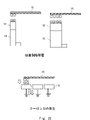
- FIG. 4 and 5 are top views schematically showing the laser irradiation pitch on the object 16 to be processed. 4 and 5 show enlarged views of the object 16 to be processed.
- FIG. 4 shows a comparative example in which the direction perpendicular to the linear laser beam is parallel to the conveying direction.
- FIG. 5 shows an embodiment in which the direction perpendicular to the line-shaped laser beam is tilted from the conveying direction.
- the edge of the object to be processed 16 and the linear laser beam are parallel.
- the edges of the object to be processed 16 are parallel to the x-direction or the y-direction.
- the laser beam irradiation line 15f is a straight line indicating the center of the laser beam irradiation area 15a, and is parallel to the longitudinal direction of the irradiation area.
- the irradiation line 15f is parallel to the y-direction, and the irradiation line 15f is orthogonal to the conveying direction of the object 16 to be processed. Since the conveying speed of the object 16 to be processed is constant, the irradiation lines 15f are arranged at regular intervals. The interval between the irradiation lines 15f is defined as an irradiation pitch.
- the irradiation pitch is determined by the repetition frequency of the pulsed laser light and the transport speed.
- the gate electrode 402 and the source electrode 407 are formed parallel to the edge of the object 16 to be processed.
- the gate electrode 402 is parallel to the y-direction and parallel to the source electrode 407 .
- the TFTs 313a are arranged along the x-direction and the y-direction.
- the manufacturing pitch of the TFTs corresponds to the spacing of the gate electrodes 402 .
- the laser irradiation pitch and the TFT manufacturing pitch are different.
- the beat of the figure causes a striped pattern, or moire, to become visible.
- the position of the irradiation line between the first laser irradiation (on the upper side in FIG. 4) and the second laser irradiation (on the lower side in FIG. 4) is deviates.
- the irradiation line 15f is inclined with respect to the conveying direction of the object 16 to be processed. Since the object to be processed 16 is transported in the direction orthogonal to the longitudinal direction of the laser beam, the periodicity of the shape appearing in the same direction is eliminated. This makes moire less visible. In this manner, as in the present embodiment, by transporting the object 16 to be processed in a direction inclined from the direction perpendicular to the longitudinal direction of the linear laser beam, it is possible to prevent moiré from occurring.
- the moire may not be eliminated, or another moire may occur.
- the angle of the irradiation line 15f may be adjusted according to the manufacturing pitch of the TFTs. Strictly speaking, the position of the irradiation line between the first laser irradiation (upper half of FIG. 4) and the second laser irradiation (lower half of FIG. 4) may deviates.
- the object 16 to be processed is transported in order to irradiate the object 16 to be processed with the linear laser beam 15 .
- the levitation unit 10 levitates the object 16 to be processed on its upper surface.
- the object to be processed 16 is held by the holding mechanism 12 .
- the holding mechanism 12 In order to change the irradiation position of the laser beam 15 on the object 16 to be processed, the holding mechanism 12 is moved in a direction tilted from the direction perpendicular to the longitudinal direction of the linear laser beam when viewed from above.
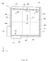
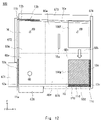
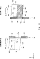
- FIG. 6 is a top view schematically showing the conveying device 600. As shown in FIG. Descriptions of the contents common to the first embodiment will be omitted as appropriate.
- the levitation unit 10 is divided into six regions 60a to 60f in top view.
- the levitation unit 10 includes a first area 60a to a fourth area 60d, a process area 60e, and a passage area 60f.
- the first region 60a is a trapezoidal region including corners on the -x side and the +y side (upper left corner in FIG. 6).
- the second region 60b is a trapezoidal region including +x and +y side corners (upper right corner in FIG. 6).
- the third area 60c is a rectangular area including the +x side and -y side corners (lower right corner in FIG. 6).
- the fourth area 60d is a rectangular area including the -x side and -y side corners (lower left corner in FIG. 6).
- the process area 60e is a trapezoidal area arranged between the first area 60a and the second area 60b.
- the process area 60e is an area including the irradiation area 15a irradiated with laser light.
- the passing area 60f is a rectangular area arranged between the third area 60c and the fourth area 60d.
- the half region on the +y side of the levitation unit 10 (upper half region in FIG. 6) becomes a first region 60a, a process region 60e, and a second region 60b in order from the ⁇ x side (left side in FIG. 6). ing.
- the -y side half area (lower half area in FIG. 6) of the levitation unit 10 is a third area 60c, a passing area 60f, and a fourth area 60d in order from the +x side.
- the levitation unit 10 includes a rotation mechanism 68 and alignment mechanisms 69a and 69b.
- a rotating mechanism 68 rotates the substrate.
- Alignment mechanisms 69a and 69b align the substrates.
- Alignment mechanisms 69a and 69b are provided in the first region 60a and the second region 60b, respectively.
- a rotation mechanism 68 is provided in the fourth area 60d. Operations of the rotation mechanism 68 and the alignment mechanisms 69a and 69b will be described later.
- the end floating units 671 to 676 are arranged outside the floating unit 10 . End floating units 671 to 676 are arranged along the outer circumference of the trapezoidal floating unit 10 . The end levitation units 671 to 676 are provided along the edge of the levitation unit 10 . The end floating units 671 to 676 are arranged so as to surround the outer periphery of the floating unit 10 when viewed from above.
- the end levitation units 671 and 672 are arranged on the -x side of the levitation unit 10 .
- An end levitation unit 673 is arranged on the +y side of the levitation unit 10 .
- An end levitation unit 674 is arranged on the +x side of the levitation unit 10 .
- End levitation units 675 , 676 are arranged on the ⁇ y side of the levitation unit 10 .
- At least one of the end floating units 671, 672, 673, 674, 675, 676 can be omitted.
- the holding mechanism 12 holds the edge of the substrate 100 .
- the levitation unit 10 levitates the portion other than the end of the proximal end. By doing so, it is possible to avoid using the end levitation units around the levitation unit 10 .
- the end levitation units 671 and 672 are arranged along the edge of the levitation unit 10 on the -x side. That is, the end floating units 671 and 672 are provided along the y direction. Also, the width of the end floating unit 671 in the x-direction is wider than that of the end floating unit 672 .
- the end floating unit 671 is arranged on the -y side of the end floating unit 672 .
- the end levitation unit 673 is arranged along the edge of the levitation unit 10 on the +y side. That is, the end floating unit 673 is provided along the inclined side 10 e of the floating unit 10 .
- the end floating unit 674 is arranged along the edge of the +x side of the floating unit 10 . That is, the end floating units 674 are provided along the y direction.
- the end levitation units 675 and 676 are arranged along the edge of the levitation unit 10 on the -y side. That is, the end levitation units 675 and 676 are provided along the x-direction. Also, the width of the end floating unit 676 in the y direction is wider than the end floating unit 675 . The end levitation unit 676 is arranged on the ⁇ x side of the end levitation unit 675 .
- a transport unit 11a is provided between the levitation unit 10 and the end levitation unit 671.
- the transport unit 11 a is also arranged between the levitation unit 10 and the end levitation unit 672 .
- the transport unit 11a is formed along the y direction.
- the transport unit 11a transports the substrate in the +y direction. That is, the transport unit 11a transports the substrate 100 from the fourth area 60d toward the first area 60a.
- a transport unit 11b is provided between the levitation unit 10 and the end levitation unit 673.
- the transport unit 11b is formed along the inclined side 10e.
- the transport unit 11b transports the substrate in a direction parallel to the inclined side 10e. That is, the transport unit 11b transports the substrate 100 from the first area 60a toward the second area 60b.
- a transport unit 11c is provided between the levitation unit 10 and the end levitation unit 674.
- the transport unit 11c is formed along the y direction.
- the transport unit 11c transports the substrate 100 in the -y direction. That is, the transport unit 11c transports the substrate 100 from the second area 60b toward the third area 60c.
- a transport unit 11d is provided between the levitation unit 10 and the end levitation unit 675.
- the transport unit 11 d is also arranged between the levitation unit 10 and the end levitation unit 676 .
- the transport unit 11d is formed along the x direction.
- the transport unit 11a transports the substrate in the -x direction. That is, the transport unit 11d transports the substrate from the third area 60c toward the fourth area 60d.
- the transport units 11a to 11d each have a holding mechanism 12 and a moving mechanism 13 as in the first embodiment. Operations of the holding mechanism 12 and the moving mechanism 13 will be described later.
- the laser light irradiation region 15a has the longitudinal direction in the y direction. That is, a line-shaped irradiation area 15a having the y direction as the longitudinal direction is formed.
- the substrate is irradiated with laser light while the substrate is being transported in a direction parallel to the inclined side 10e. While moving from the first area 60a to the second area 60b, a laser irradiation process is performed.
- the amorphous silicon film is converted into the polysilicon film by irradiating the substrate with laser light from the laser generator.
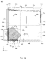
- a precision levitation unit 111 is arranged in the irradiation area 15a and its periphery.
- the precision levitation unit 111 has a higher precision of the levitation amount than the semi-precision levitation unit and the rough levitation unit in other areas. Therefore, in the process area 60e including the irradiation area 15a, the laser beam is applied to the object to be processed while floating with a higher accuracy of flying height than the other areas 60a to 60d and 60f. This makes it possible to stably irradiate the object to be processed with the laser beam. Areas other than the irradiation area 15a, such as the passing area 60f, the third area 60c, and the fourth area 60d, are created without using the expensive precision levitation unit 111. FIG. Therefore, device cost can be reduced.
- the fourth area 60d serves as the loading position and the unloading position of the substrate 100.
- the substrate 100 carried into the fourth area 60d is transferred to the first area 60a, the process area 60e, the second area 60b, the third area 60c, the passing area 60f, and the fourth area 60d in this order. It will be done. That is, the substrate 100 goes around along the edge of the levitation unit 10 .
- the substrate 100 makes two turns. That is, the substrate 100 is conveyed so as to circulate twice on the floating unit 10 . By doing so, almost the entire surface of the substrate 100 is irradiated with laser light.
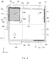
- the substrate 100 is loaded into the fourth area 60d.
- the substrate 100 carried into the fourth area 60 d is floated by the levitation unit 10 and the edge levitation units 671 , 672 and 676 . That is, the ⁇ x side edge of the substrate 100 is floated by the edge levitation units 671 and 672 , and the central portion is levitated by the levitation unit 10 .
- the ⁇ y side edge of the substrate 100 is floated by the edge levitation unit 676 .
- the substrate 100 is held by the holding mechanism 12a of the transport unit 11a.
- the substrate 100a in the fourth area 60d is transferred to the first area 60a.
- the substrate moved to the first region 60a is shown as the substrate 100b.
- a holding mechanism 12a of the transport unit 11a holds the substrate 100a.
- the substrate 100a moves from the fourth area 60d to the first area 60a by moving the holding mechanism 12a in the +y direction by the moving mechanism 13a (white arrow in FIG. 8).
- the holding mechanism 12a passes between the floating unit 10 and the end floating unit 671 and moves in the +y direction. Furthermore, in the xy plan view, the holding mechanism 12a moves in the +y direction through between the levitation unit 10 and the end levitation unit 672 . Therefore, the substrate 100b is levitated by the levitation unit 10 and the end levitation units 672,673. That is, the ⁇ x-side edge of the substrate 100 b is floated by the edge floating unit 672 , and the central portion is floated by the floating unit 10 . The edge on the +y side of the substrate 100 b is floated by the edge levitation unit 673 .
- the alignment mechanism 69a aligns the position and angle of the substrate 100b transferred to the first region 60a.
- the position and rotation angle of the substrate may be slightly deviated due to the loading operation, the transport operation, and the rotating operation of the substrate 100 .
- the alignment mechanism 69a corrects deviations in position and rotation angle. Thereby, the irradiation position of the laser light on the substrate 100 can be controlled with high accuracy.
- the alignment mechanism 69a is movable in the y-direction and rotatable around the z-axis. Furthermore, the alignment mechanism 69a is movable in the z-direction.
- the alignment mechanism 69a has an actuator such as a motor. The amount of positional deviation and the amount of angular deviation are obtained from an image of the substrate 100b captured by a camera or the like. The alignment mechanism 69a performs alignment based on this deviation amount.
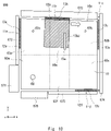
- An alignment mechanism 69a is arranged directly below the central portion of the substrate 100b. Alignment mechanism 69a holds substrate 100b. The alignment mechanism 69a may suck and hold the substrate 100b in the same manner as the holding mechanism 12 does. The holding mechanism 12a releases the holding of the substrate 100b. As a result, the substrate 100b is transferred from the holding mechanism 12a to the alignment mechanism 69a.
- the alignment mechanism 69a rotates the substrate 100b around the z-axis (white arrow in FIG. 9).
- the alignment mechanism 69 a rotates the substrate 100 b so that the edge of the substrate 100 b is parallel to the inclined side 10 e of the floating unit 10 .
- the substrate after rotation is shown as substrate 100c.
- the alignment mechanism 69a rotates the substrate 100 about 5 degrees around the z-axis.
- the edge of the substrate 100c is parallel to the inclined side 10e of the levitation unit 10.
- the holding mechanism 12b of the transport unit 11b holds the substrate 100b, and the alignment mechanism 69a releases the holding.
- the substrate 100c is transferred from the alignment mechanism 69a to the holding mechanism 12b of the transport unit 11b.
- the transport unit 11b moves the substrate 100d.
- This causes the substrate 100d to pass through the process area 60e.
- the holding mechanism 12b passes between the levitation unit 10 and the end levitation unit 673 and moves in a direction parallel to the inclined side 10e.
- almost half the area of the substrate 100d passes through the irradiation area 15a.
- a substrate 100d that is moving in a tilt direction that is tilted from the x-direction orthogonal to the irradiation region 15a is irradiated with laser light.
- the holding mechanism 12b passes between the levitation unit 10 and the end levitation unit 673 and moves in a direction parallel to the inclined side 10e. Therefore, the substrate 100 d is levitated by the levitation unit 10 and the end levitation unit 673 . In other words, the +y side edge of the substrate 100d is floated by the edge levitation unit 673, and the central part is levitated by the levitation unit .
- a laser irradiation process is performed while moving from the first region 60a to the second region 60b.
- the alignment mechanism 69b aligns the substrate 100e.
- the alignment mechanism 69b rotates the substrate 100e (white arrow in FIG. 11).
- the substrate after rotation is shown as a substrate 100f.
- An alignment mechanism 69b is arranged directly below the central portion of the substrate 100e. Alignment mechanism 69b holds substrate 100e. The alignment mechanism 69b may suck and hold the substrate 100e in the same manner as the holding mechanism 12 does. Furthermore, the holding mechanism 12b releases the holding of the substrate 100e. The substrate 100e is transferred from the holding mechanism 12b of the transport unit 11b to the alignment mechanism 69b.
- the alignment mechanism 69b rotates the substrate 100e around the z-axis (white arrow in FIG. 11).
- the alignment mechanism 69a rotates the substrate 100e such that the edge of the substrate 100e is parallel to the inclined side 10e of the floating unit 10.
- FIG. The edge of the substrate 100f after rotation is parallel to the x-direction or the y-direction.
- the holding mechanism 12c of the transport unit 11c holds the substrate 100f, and the alignment mechanism 69b releases the holding. As a result, the substrate 100f is transferred from the alignment mechanism 69b to the holding mechanism 12c of the transport unit 11c.
- the substrate 100 e is levitated by the levitation unit 10 and end levitation units 673 and 674 . That is, the +y side edge of the substrate 100 e is floated by the edge floating unit 673 . The edge on the +x side of the substrate 100 e is floated by the edge levitation unit 674 , and the central part is levitated by the levitation unit 10 .
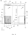
- the substrate 100f in the second area 60b is transferred to the third area 60c.
- the substrate moved to the third region 60c is shown as substrate 100g.
- the holding mechanism 12c of the transport unit 11c holds the substrate 100f.
- the substrate 100f moves from the second area 60b to the third area 60c by moving the holding mechanism 12c in the -y direction by the moving mechanism 13c (white arrow in FIG. 12).
- the holding mechanism 12c passes between the floating unit 10 and the end floating unit 674 and moves in the -y direction. Therefore, the substrate 100 e is levitated by the levitation unit 10 and the end levitation units 674 and 675 .
- the edge on the +x side of the substrate 100 e is floated by the edge levitation unit 674 , and the central part is levitated by the levitation unit 10 .
- the ⁇ y side edge of the substrate 100 e is floated by the edge levitation unit 675 .
- the holding mechanism 12d of the transport unit 11d holds the substrate 100g, and the holding mechanism 12c releases the holding.
- the substrate 100g is transferred from the holding mechanism 12c of the transport unit 11c to the holding mechanism 12d of the transport unit 11d.
- the substrate 100g in the third area 60c is transferred to the fourth area 60d.
- the substrate moved to the fourth region 60d is shown as substrate 100h.
- the holding mechanism 12d of the transport unit 11d holds the substrate 100g.
- the moving mechanism 13d moves the holding mechanism 12d in the -x direction, thereby moving the substrate 100f from the third region 60c to the fourth region 60d (white arrow in FIG. 13).
- the holding mechanism 12d passes between the levitation unit 10 and the end levitation unit 675 and moves in the -x direction.
- the holding mechanism 12d passes between the levitation unit 10 and the end levitation unit 676 and moves in the -x direction. Therefore, the substrate 100 h is levitated by the levitation unit 10 and the edge levitation unit 676 .
- the ⁇ y side edge of the substrate 100 h is floated by the edge levitation unit 676
- the central part is levitated by the levitation unit 10 .
- the ⁇ x side edge of the substrate 100 h is floated by the edge floating unit 671 .
- the substrate 100 that was in the fourth region 60d becomes the first region 60a, the process region 60e, the second region 60b, the third region 60c, the passing region 60f, and the fourth region 60d. Move in order. That is, the substrate 100 goes around along the edge of the levitation unit 10 .
- the rotation mechanism 68 rotates the substrate 100h around the z-axis by 180 degrees. That is, the substrate 100h is transferred from the holding mechanism 12d to the rotating mechanism 68.
- FIG. When the rotation mechanism 68 rotates the substrate 100h, the substrate 100h is transferred from the rotation mechanism 68 to the holding mechanism 12d.
- the transport units 11a to 11d again move the substrate 100h through the first region 60a, the process region 60e, the second region 60b, the third region 60c, the passing region 60f, and the fourth region 60d. continue. That is, as shown in FIGS. 7 to 13, the substrate 100 goes around along the edge of the levitation unit .
- the rotation mechanism 68 rotates the substrate 100h by 180°.
- the laser light is applied to the remaining half area that was not irradiated with the laser light during the first pass.
- the substrate 100 circulates twice along the edge of the levitation unit 10 . Since the substrate 100 is rotated by 180° between the first laser irradiation and the second laser irradiation, almost the entire surface of the substrate 100 is irradiated with laser light.
- the position to rotate the substrate 100 is not limited to the first region 60a. For example, it may be performed in the second region 60b, the third region 60c, the fourth region 60d, or the like.
- the moving mechanism 13b conveys the holding mechanism 12b in a direction inclined from the x-direction orthogonal to the irradiation area 15a. Therefore, the crystallization process of the silicon film can be properly performed. For example, it is possible to prevent the occurrence of moiré and improve the display quality.
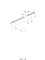
- FIG. 15 is a perspective view showing the configuration of part of the holding mechanism 12. As shown in FIG. FIG. 15 shows a holding mechanism 12 whose moving direction is the y-direction, like the holding mechanism 12c shown in FIG. 13, for example. FIG. 15 shows the configuration of the ⁇ y side end of the holding mechanism 12 .
- the holding mechanism 12 includes a plurality of adsorption cells 121.
- a plurality of adsorption cells 121 are arranged along the transport direction.
- a recess 122 is provided between the two adsorption cells 121 .
- the holding mechanism 12 is made of, for example, a metal material such as aluminum.
- a plurality of adsorption cells 121 can be integrally formed from an aluminum alloy such as A5052.
- the upper surface of the adsorption cell 121 serves as an adsorption surface 121a for adsorbing the substrate 100 (not shown in FIG. 15).
- 16 shows an enlarged view of the adsorption surface 121a and a sectional view of the adsorption cell 121.
- FIG. A suction groove 126 is provided on the suction surface 121a. Furthermore, the suction groove 126 is connected to the suction hole 125 .
- An intake hole 125 is connected to an internal space 127 provided in the adsorption cell 121 . When the internal space 127 is evacuated by a pump or the like, the suction holes 125 and the suction grooves 126 become negative pressure. As a result, the substrate 100 is vacuum-sucked on the suction surface 121a of each suction cell 121 .
- a valve 129 is preferably provided for each of the plurality of adsorption cells 121, as shown in FIG.
- each adsorption cell 121 is connected to an exhaust port 128 .
- Exhaust port 128 is connected to pipe 130 via valve 129 .
- a pipe 130 is common to the plurality of exhaust ports 128 .
- the pipe 130 is connected to exhaust means 131 such as a vacuum pump and an ejector. Therefore, the evacuation means 131 can depressurize the internal space 127 of each adsorption cell 121 .
- a valve 129 is provided for each adsorption cell 121 .
- a plurality of valves 129 can be opened and closed independently.
- a substrate 100 is placed on the adsorption surface 121a. By opening all the valves 129 , each adsorption cell 121 vacuum-sucks the lower surface of the substrate 100 .
- the substrate 100 may not cover the adsorption surface 121a of some of the adsorption cells 121 due to the transportation error of the substrate 100 .
- the adsorption surface 121 a of the adsorption cell 121 may not be completely covered with the substrate 100 .
- the valve 129 of the adsorption cell 121 whose adsorption surface 121a is not closed is closed.
- the substrate 100 is shifted from the adsorption surface 121a. Therefore, the valve 129 of the right adsorption cell 121 is closed.
- FIG. 18 in the right adsorption cell 121 of the two adsorption cells 121, the substrate 100 is shifted from the adsorption surface 121a. Therefore, the valve 129 of the right adsorption cell 121 is closed.
- the substrate 100 is held only by the adsorption cell 121 on the left side.
- the valve 129 is closed when the suction flow rate of the gas at the exhaust port 128 exceeds a threshold value. By doing so, the substrate 100 can be properly vacuum-sucked. Therefore, it is possible to transport the substrate suitable for the laser irradiation process.
- FIG. 19 is a side view schematically showing an example of the overall configuration of the conveying device 600.
- the carrier device 600 includes an area base 610 , a pedestal 620 and a carrier stage 630 . Further, the transport device 600 includes the levitation unit 10, the holding mechanism 12, the moving mechanism 13, and the end levitation unit 670 as described above. As shown in FIG. 17 and the like, a pipe 130 is connected to the holding mechanism 12 by a joint or the like.
- An area base 610 is provided on the pedestal 620 .
- a levitation unit 10 and an end levitation unit 670 are provided on the area base 610 .
- the end levitation unit 670 is any of the end levitation units 671-676 illustrated in FIGS.
- the levitation unit 10 includes a semi-precision levitation unit 112 and a rough levitation unit 113 .
- the semi-precision levitation unit 112 has lower levitation accuracy than the precision levitation unit 111 .
- the rough levitation unit 113 has lower levitation accuracy than the semi-precision levitation unit 112 and the precision levitation unit 111 .
- a holding mechanism 12 is arranged between the levitation unit 10 and the end levitation unit 670 .
- the moving mechanism 13 is arranged on the carrier stage 630 .
- the moving mechanism 13 has a guide mechanism and the like provided along the moving direction.
- the moving mechanism 13 moves the holding mechanism 12 as described above. Therefore, the holding mechanism 12 moves along the edge of the levitation unit 10 in the space (gap) between the levitation unit 10 and the end levitation unit 670 .
- the moving substrate 100 can be irradiated with laser light.
- FIG. 20 is a top view schematically showing the configuration of the conveying device 600A.
- the levitation unit is divided into a first levitation unit 10A and a second levitation unit 10B in order to transport a larger substrate 100 .
- the substrate 100 is a glass substrate of G10 size (3130 mm ⁇ 2880 mm).
- the configuration other than the first levitation unit 10A and the second levitation unit 10B is the same as that of the first and second embodiments, and thus the description thereof will be omitted as appropriate.
- a gap 10C is provided between the first floating unit 10A and the second floating unit 10B. That is, the first floating unit 10A and the second floating unit 10B are arranged with a gap 10C therebetween.
- the first floating unit 10A and the second floating unit 10B are arranged below the substrate 100, which is the object to be processed, as shown in the first and second embodiments. Then, the first floating unit 10A and the second floating unit 10B eject gas onto the lower surface of the substrate 100, thereby floating the substrate 100 in the air.
- Laser light is applied while the floating substrate 100 is being moved.
- the irradiation area 15a of the laser light has a line shape along the y direction.
- the irradiation area 15a is formed in the first floating unit 10A.
- the holding mechanism 12 is moved along the x direction by the moving mechanism 13 (not shown in FIG. 20).
- the transport direction of the substrate 100 is parallel to the x direction.
- the holding mechanism 12 moves along the gap 10C.
- the holding mechanism 12 sucks and holds the central portion of the substrate 100 that is not the end portion.
- the first levitation unit 10A is arranged from the central portion of the substrate 100 to one end side.
- the second floating unit 10B is arranged from the central portion of the substrate 100 to the other end side.
- the first floating unit 10A is arranged on the -y side of the holding mechanism 12, and the second floating unit 10B is arranged on the +y side of the holding mechanism 12. Therefore, the first floating unit 10A air-floats from the central portion of the substrate 100 to the edge on the -y side.
- the second levitation unit 10B air levitates from the central portion of the substrate 100 to the edge on the +y side.
- the first levitation unit 10A and the second levitation unit 10B for air-levitating the central portion of the substrate 100 are provided.
- the holding mechanism 12 holds the inner portion of the substrate 100 that is not the edge.
- FIG. 21 is a diagram for explaining the case where the edge of the substrate 100 is held.
- a moment of inertia M acts on the portion held by the holding mechanism 12.
- the moment of inertia M becomes larger than when the holding mechanism 12 holds the central portion of the substrate 100 .
- the moment of inertia M increases. If the moment of inertia M becomes large, there is a possibility that the holding mechanism 12 will be released from the vacuum adsorption.
- the adsorption force can be increased by increasing the width of the holding mechanism 12 in the y direction.
- increasing the width of the holding mechanism 12 increases the contact area where the substrate 100 and the holding mechanism 12 contact each other. Therefore, as shown in FIG. 22, charging of the substrate 100 becomes a problem.
- the substrate 100 is charged due to adsorption/separation electrification that occurs when the substrate 100 is destroyed by adsorption (the upper diagram in FIG. 22).
- the charge amount increases in proportion to the contact area between the substrate 100 and the holding mechanism 12 .
- the holding mechanism 12 is made of a metal material. By grounding the holding mechanism 12, the charge of the holding mechanism 12 can be released.
- the substrate 100 is an insulator such as glass. Therefore, the charges of the charged substrate 100 stay on the substrate 100 .
- a Coulomb force is generated between the substrate 100 and the levitation unit 10, and the substrate 100 is drawn toward the levitation unit 10 (lower diagram in FIG. 22). In this case, the substrate 100 and the levitation unit 10 may come into contact with each other and be damaged.
- the holding mechanism 12 holds the central portion of the substrate 100 instead of the end portions. By doing so, the moment of inertia generated in the portion held by the holding mechanism 12 can be reduced, so the planar size of the holding mechanism 12 can be reduced. In other words, even when the planar size of the holding mechanism 12 is reduced, it is possible to prevent the substrate 100 from being sucked and held due to the moment of inertia.
- the holding mechanism 12 holds the central portion of the substrate 100 instead of the edge portions. That is, when viewed from above, the second floating unit 10B is arranged from the edge of the substrate 100 to the central portion.
- the central portion of the substrate 100 can be, for example, a position where the substrate 100 bends and contacts the second levitation unit 10B when the second levitation unit 10B does not eject gas. That is, when the holding mechanism 12 holds the central portion of the substrate 100 and stops the release of the gas from the second floating unit 10B while the substrate is being transported, the substrate 100 comes into contact with the second floating unit 10B.
- the edge of the substrate 100 is, for example, a position that does not contact the second levitation unit 10B even if the substrate 100 bends when the second levitation unit 10B does not eject gas. can be done. Even if the release of gas from the second levitation unit 10B is stopped while the holding mechanism 12 is holding the edge of the substrate 100, the substrate 100 does not come into contact with the second levitation unit 10B.
- the transport method according to the present embodiment transports the substrate 100 in order to irradiate the substrate 100 with laser light that forms the linear irradiation area 15a.
- One end side of the substrate 100 is floated from the central portion of the substrate 100 in top view using the first floating unit 10A arranged below the substrate 100, and the second floating unit arranged below the substrate 100 is used.
- 10B is used to levitate the other end side of the substrate 100 from the central portion of the substrate 100 in top view.
- a holding mechanism 12 arranged below the central portion of the substrate 100 is used to suck and hold the substrate 100 .
- the holding mechanism 12 is moved along the gap 10C between the first floating unit 10A and the second floating unit 10B.
- FIG. FIGS. 23 to 25 schematically show irradiation positions of the laser beam on the substrate 100, respectively.
- substrate 100 is a mother glass substrate for forming a plurality of display panels.
- the substrate size is 3130 mm ⁇ 2880 mm.
- Example 1 shown in FIG. 23 shows an example of 8-panel fabrication in which eight display panels P1 to P8 are manufactured from one substrate 100.
- the substrate size in the x direction is 3130 mm
- the substrate size in the y direction is 2880 mm.
- the panel size of each display panel is 764 mm ⁇ 1341 mm.
- the size of the irradiation area 15a in the y direction shall be 1341 mm or more.
- Almost half of the substrate 100 is irradiated with the laser light by irradiating the substrate 100 while the substrate 100 is being transported in the x-direction. In the region irradiated with the laser light, the amorphous silicon film is crystallized to form a polysilicon film.
- a polysilicon film can be formed on almost the entire substrate 100 by two irradiation processes.
- the substrate 100 In the first irradiation process, almost half the area of the substrate 100 is irradiated with laser light. That is, in the first irradiation process, a half rectangular area on the one end side of the substrate 100 is irradiated with laser light. A laser beam is applied to regions that will be the display panels P1 to P4. In the first irradiation process, the substrate 100 is transported in the x-direction while the holding mechanism 12 (not shown in FIG. 23) holds one or more regions of the display panels P5 to P8.
- the substrate 100 is rotated 180° around the z-axis.
- the remaining half region of the substrate 100 is irradiated with laser light. That is, in the second irradiation process, the half rectangular area on the other end side of the substrate 100 is irradiated with laser light.
- a laser beam is applied to the regions to be the display panels P5 to P8.
- the substrate 100 is transported in the x direction while the holding mechanism 12 holds an area that will be one or more of the display panels P1 to P4. Almost the entire surface of the substrate 100 is irradiated with laser light by two irradiation processes.
- Embodiment 2 shown in FIG. 24 shows an example of 6-panel fabrication in which six display panels P1 to P6 are manufactured from one substrate 100.
- the substrate size in the x direction is 3130 mm
- the substrate size in the y direction is 2880 mm.
- the panel size of each display panel is 1546 mm ⁇ 888 mm.
- the size of the irradiation area 15a in the y direction shall be 888 mm or more.
- the substrate 100 In the first irradiation process, approximately 1 ⁇ 3 area of the substrate 100 is irradiated with laser light. A 1 ⁇ 3 rectangular area on one end side of the substrate 100 is irradiated with laser light. In other words, the laser light is applied to the regions to be the display panels P1 and P2. In the first irradiation process, the substrate 100 is transported in the x-direction while the holding mechanism 12 (not shown in FIG. 24) holds one or more regions of the display panels P3 to P6.
- the substrate 100 is transported in the -y direction.
- approximately one-third of the center area of the substrate 100 is irradiated with laser light.
- a 1 ⁇ 3 rectangular area including the center of the substrate 100 is irradiated with laser light.
- a laser beam is applied to the regions to be the display panels P3 and P4.
- the substrate 100 is transported in the x direction while the holding mechanism 12 holds an area that will be one or more of the display panels P5 and P6. Approximately two-thirds of the substrate 100 is irradiated with laser light by two irradiation processes.
- the substrate 100 is rotated 180° around the z-axis and transported in the y-direction.
- a 1 ⁇ 3 rectangular area on the other end side of the substrate 100 is irradiated with laser light.
- a laser beam is applied to the regions to be the display panels P5 and P6.
- the substrate 100 is transported in the x direction while the holding mechanism 12 holds an area that will be one or more of the display panels P1 to P4. Almost the entire substrate 100 is irradiated with laser light by three irradiation processes.
- the order of laser light irradiation processes is not particularly limited. For example, after irradiating the regions to be the display panels P5 and P6 with the laser light, the regions to be the display panels P3 and P4 may be irradiated with the laser light. Also, in the first irradiation process, the regions to be the display panels P3 and P4 may be irradiated with laser light.
- Example 3 shown in FIG. 25 shows an example of 6-panel fabrication in which three display panels P1 to P3 are manufactured from one substrate 100.
- the substrate size in the x direction is 2880 mm
- the substrate size in the y direction is 3130 mm.
- the panel size of each display panel is 1806 mm ⁇ 1029 mm.
- the size of the irradiation area 15a in the y direction shall be 1029 mm or more.
- the substrate 100 In the first irradiation process, approximately 1 ⁇ 3 area of the substrate 100 is irradiated with laser light. A 1 ⁇ 3 rectangular area on one end side of the substrate 100 is irradiated with laser light. In other words, the laser light is applied to the area that will be the display panel P1. In the first irradiation process, the substrate 100 is transported in the x-direction while the holding mechanism 12 (not shown in FIG. 25) holds one or more regions of the display panels P1 and P2.
- the substrate 100 is transported in the -y direction.
- approximately one-third of the center area of the substrate 100 is irradiated with laser light.
- a 1 ⁇ 3 rectangular area including the center of the substrate 100 is irradiated with laser light.
- a laser beam is applied to a region that will be the display panel P2.
- the substrate 100 is transported in the x direction while the holding mechanism 12 holds an area that will be one or more of the display panels P1 and P3. Approximately two-thirds of the substrate 100 is irradiated with laser light by two irradiation processes.
- the substrate 100 is rotated 180° around the z-axis and transported in the y-direction.
- a 1 ⁇ 3 rectangular area on the other end side of the substrate 100 is irradiated with laser light.
- a laser beam is applied to a region that will become the display panel P3.
- the substrate 100 is transported in the x direction while the holding mechanism 12 holds an area that will be one or more of the display panels P1 and P2. Almost the entire substrate 100 is irradiated with laser light by three irradiation processes.
- the order of laser light irradiation processes is not particularly limited. For example, after irradiating the regions to be the display panels P5 and P6 with the laser light, the regions to be the display panels P3 and P4 may be irradiated with the laser light. Also, in the first irradiation process, the regions to be the display panels P3 and P4 may be irradiated with laser light.
- the holding mechanism 12 holds the substrate 100 at a position about 1 ⁇ 3 of the substrate size from the edge of the substrate 100 . That is, the second floating unit 10B has a width of about 1 ⁇ 3 of the substrate size of the substrate 100 in the y direction. Of course, the width of the second floating unit 10B is not limited to 1/3 of the substrate size.
- the size of the second floating unit 10B may be determined by determining the number of processes according to the size of the substrate, the number of chamfers of the panel, and the size of the laser beam irradiation area 15a. For example, each of the first levitation unit 10A and the second levitation unit 10B may be 1/4 or more of the substrate size.
- a large substrate 100 can be properly transported by the configuration of the present embodiment. Even if a rotating force is applied to the substrate 100, the moment of inertia can prevent the cancellation of the adsorption and holding. Moreover, since the substrate 100 can be reliably held with a small adsorption area, an increase in the amount of charge can be prevented. Therefore, the Coulomb force allows the substrate 100 to come into contact with the first floating unit 10A or the second floating unit 10B.
- the configuration of Embodiment 3 can be appropriately combined with the configurations of Embodiments 1 and 2.
- the transport direction of the substrate 100 may be a direction inclined from the longitudinal direction of the irradiation region 15a.
- a semiconductor device having the above polysilicon film is suitable for a TFT (Thin Film Transistor) array substrate for an organic EL (ElectroLuminescence) display. That is, the polysilicon film is used as a semiconductor layer having a source region, a channel region and a drain region of the TFT.
- TFT Thin Film Transistor
- organic EL ElectroLuminescence
- FIG. 26 is a cross-sectional view showing a simplified pixel circuit of an organic EL display.
- the organic EL display 300 shown in FIG. 26 is an active matrix display device in which a TFT is arranged in each pixel PX.
- the organic EL display 300 includes a substrate 310 , a TFT layer 311 , an organic layer 312 , a color filter layer 313 and a sealing substrate 314 .
- FIG. 26 shows a top emission type organic EL display in which the sealing substrate 314 side is the viewing side. Note that the following description shows one configuration example of the organic EL display, and the present embodiment is not limited to the configuration described below.
- the semiconductor device according to this embodiment may be used in a bottom emission type organic EL display.
- the substrate 310 is a glass substrate or a metal substrate.
- a TFT layer 311 is provided on the substrate 310 .
- the TFT layer 311 has a TFT 311a arranged in each pixel PX. Further, the TFT layer 311 has wiring (not shown) and the like connected to the TFT 311a.
- the TFT 311a, wiring, and the like constitute a pixel circuit.
- An organic layer 312 is provided on the TFT layer 311 .
- the organic layer 312 has an organic EL light emitting element 312a arranged for each pixel PX. Further, the organic layer 312 is provided with partition walls 312b for separating the organic EL light emitting elements 312a between the pixels PX.
- a color filter layer 313 is provided on the organic layer 312 .
- the color filter layer 313 is provided with color filters 313a for color display. That is, each pixel PX is provided with a resin layer colored R (red), G (green), or B (blue) as a color filter 313a.
- a sealing substrate 314 is provided on the color filter layer 313 .
- the sealing substrate 314 is a transparent substrate such as a glass substrate, and is provided to prevent deterioration of the organic EL light emitting element of the organic layer 312 .
- the current flowing through the organic EL light emitting element 312a of the organic layer 312 changes depending on the display signal supplied to the pixel circuit. Therefore, by supplying a display signal corresponding to a display image to each pixel PX, the amount of light emitted from each pixel PX can be controlled. Thereby, a desired image can be displayed.
- one pixel PX is provided with one or more TFTs (for example, a switching TFT or a driving TFT).
- TFTs for example, a switching TFT or a driving TFT.
- a semiconductor layer having a source region, a channel region, and a drain region is provided in the TFT of each pixel PX.
- the polysilicon film according to this embodiment is suitable for a semiconductor layer of a TFT. That is, by using the polysilicon film manufactured by the above-described manufacturing method as the semiconductor layer of the TFT array substrate, it is possible to suppress in-plane variations in TFT characteristics. Therefore, a display device with excellent display characteristics can be manufactured with high productivity.
- a method of manufacturing a semiconductor device using the laser irradiation apparatus according to this embodiment is suitable for manufacturing a TFT array substrate.
- a method of manufacturing a semiconductor device having a TFT will be described with reference to FIGS. 27 and 28.
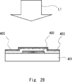
- FIG. 27 and 28 are process cross-sectional views showing the manufacturing process of the semiconductor device. In the following description, a method of manufacturing a semiconductor device having an inverted staggered type TFT will be described.
- 27 and 28 show the process of forming a polysilicon film in the semiconductor manufacturing method. For other manufacturing steps, a known method can be used, so the description is omitted.
- a gate electrode 402 is formed on a glass substrate 401 .
- a gate insulating film 403 is formed on the gate electrode 402 .
- An amorphous silicon film 404 is formed on the gate insulating film 403 .
- the amorphous silicon film 404 is arranged so as to overlap the gate electrode 402 with the gate insulating film 403 interposed therebetween.
- the gate insulating film 403 and the amorphous silicon film 404 are continuously formed by CVD (Chemical Vapor Deposition).
- a polysilicon film 405 is formed as shown in FIG. That is, the amorphous silicon film 404 is crystallized by the laser irradiation apparatus 1 shown in FIG. 1 and the like. As a result, a polysilicon film 405 of crystallized silicon is formed on the gate insulating film 403 .
- the polysilicon film 405 corresponds to the polysilicon film described above.
- the laser annealing apparatus irradiates the amorphous silicon film with the laser beam to form the polysilicon film. It may form a microcrystalline silicon film.
- the laser light for annealing is not limited to the Nd:YAG laser.
- the method according to this embodiment can also be applied to a laser annealing apparatus for crystallizing thin films other than silicon films. That is, the method according to the present embodiment can be applied to any laser annealing apparatus that irradiates an amorphous film with a laser beam to form a crystallized film. According to the laser annealing apparatus according to the present embodiment, the crystallized film-coated substrate can be appropriately modified.
- FIG. 29 is a top view schematically showing the laser irradiation device 1.
- FIG. 29 Since the basic configurations of the conveying device and the laser irradiation device 1 are the same as those of the first embodiment, description thereof will be omitted as appropriate.
- the angle of the object 16 to be processed is different from that in the first embodiment when viewed from above.
- the edge 161 on the -y side of the object to be processed 16 is inclined from the transport direction. That is, the conveying direction and the edge 161 are not parallel.
- the object to be processed 16 is rotated around the Z-axis as compared with the configuration of FIG.
- the angle between the y-direction and the edge 161 of the object 16 to be processed is defined as ⁇ .
- ⁇ be the angle between the x direction and the transport direction. Although ⁇ is greater than ⁇ here, ⁇ may be less than or equal to ⁇ .
- ⁇ is preferably larger than 0° and 5° or less. Also, ⁇ is preferably greater than 0° and 5° or less. ⁇ can be adjusted according to the specifications of the laser irradiation process.
- the alignment mechanism 69a can change the angle of the substrate 100 to a desired angle. That is, as shown in FIG. 9, the alignment mechanism 69a functions as a drive mechanism that rotates around the Z axis. The alignment mechanism 69a makes the angle of the edge of the substrate 100 different from the transport direction. By doing so, the substrate 100 can be rotated around the Z-axis before laser light irradiation.
- the transport device 600 can transport the substrate 100 while being inclined at a desired angle with respect to the linear laser beam. After irradiation with the laser light, the alignment mechanism 69b rotates the substrate 100 on the floating unit 10 as shown in FIG. By doing so, as shown in FIG. 12, the X direction and the edge of the substrate 100 become parallel.
- the laser irradiation device 1 according to Modification 2 has a slit mechanism 30 .
- the edge on the +x side is edge 162
- the edge on the -x side is edge 163
- the edge on the +y side is edge 164.
- the conveying direction is inclined from the edges 161 and 164 of the object 16 to be processed, as in FIG.
- a region 168 and a region 169 of the object 16 to be processed are sequentially irradiated with laser light. Specifically, a laser beam is applied to a half region 168 on one side of the object 16 to be processed in the first transport.
- a region 168 is a region surrounded by the edge 162 , the edge 163 , the edge 161 and the boundary line 165 .
- the boundary line 165 is a straight line parallel to the transport direction.
- the object 16 to be processed is rotated by 180° around the Z axis, it is conveyed for the second time.
- the remaining one-half region 169 is irradiated with laser light. That is, a polysilicon film is formed in the region 168 by the first laser irradiation, and a polysilicon film is formed in the region 169 by the second laser irradiation.
- a region 169 is a region surrounded by the edge 162 , the edge 163 , the edge 164 and the boundary line 165 . Also, the area 168 and the area 169 may partially overlap. In this case, in the vicinity of the boundary line 165, the object to be processed 16 is irradiated with the laser beam twice.
- a gap may be provided between the region 168 irradiated with the laser light in the first irradiation and the region 169 irradiated with the laser light in the second irradiation.
- the gap between the regions 168 and 169 may be made as narrow as possible.
- the boundary line that defines the region 168 that has been irradiated by the first irradiation does not match the boundary line that defines the region 169 that has been irradiated by the second irradiation.
- the slit mechanism 30 can adjust the length of the laser beam irradiation region 15a on the object 16 to be processed.
- the slit mechanism 30 is a variable length slit whose slit length is variable.
- the sizes of the regions 168 and 169 irradiated by the first and second laser irradiation can be freely changed.
- the slit mechanism 30 can change the length of the linear irradiation area 15a in the y direction by adjusting the slit length.
- the slit mechanism 30 is installed in the optical system of the laser irradiation section 14 shown in FIG.
- the slit mechanism 30 includes a light shielding section 32 and a light shielding section 33 .
- the light shielding part 33 and the light shielding part 32 have a light shielding plate or the like provided so as to be movable along the y direction.
- the light shielding part 33 and the light shielding part 32 can shield the edge of the laser beam.
- the light blocking portion 33 blocks the -y side end of the line beam. That is, the light shielding portion 33 defines the position on the -y side of the linear irradiation area 15a.
- the light shielding portion 32 shields the +y side end of the line beam. That is, the light shielding portion 32 defines the position on the +y side of the linear irradiation area 15a. Therefore, the position of the light blocking portion 32 defines the position of the boundary line 165 .
- the slit length can be shortened by moving the light shielding part 32 and the light shielding part 33 closer to each other in the y direction.
- the slit length can be lengthened by moving in the y direction so that the light shielding portion 32 and the light shielding portion 33 are separated from each other.
- the positions of the light shielding unit 32 and the light shielding unit 33 are determined by the optical system. will be described as the position when projected onto .
- the position of the light blocking portion 32 corresponds to the +y side end of the irradiation region 15a
- the position of the light blocking portion 33 corresponds to the ⁇ y side end of the irradiation region 15a.
- the light shielding part 33 and the light shielding part 32 move independently. This allows the slit mechanism 30 to change the line beam length and the irradiation end position on the object 16 to be processed. Furthermore, the light shielding part 33 and the light shielding part 32 may be moved in conjunction with the transportation of the object 16 to be processed. That is, the positions of the light shielding portions 32 and 33 may be changed according to the change in the transport position of the object 16 to be processed. In FIG. 30, the conveying direction is inclined from the edge 161 of the object 16 to be processed, as in FIG. 29, but it may be parallel as shown in FIG.
- FIG. 31 is a top view schematically showing a laser beam irradiation region 15a on the object 16 to be processed.
- the conveying unit 11 and the levitation unit 10 are appropriately omitted for simplification of explanation.
- the edges 161 and 164 of the object 16 to be processed and the transport direction are parallel.
- a boundary line 165 between the area 169 and the area 168 is parallel to the conveying direction and the edge 161 .
- the left side of FIG. 31 shows the configuration at the start of irradiation when the first irradiation starts, and the right side of FIG. 31 shows the configuration at the end of irradiation when the first irradiation ends.
- the irradiation start time indicates the timing when the irradiation region 15a overlaps the edge 162 of the object 16 to be processed due to transportation.
- the irradiation end point indicates the timing at which the irradiation region 15a passes the edge 163 on the -x side of the object 16 to be processed during transportation.
- the positions of the light shielding part 32 and the light shielding part 33 are constant during the first irradiation.
- the slit length and the irradiation end position are constant from the irradiation start point to the irradiation end point.
- the position of the light shielding part 33 is adjusted so that the edge position on the -y side of the irradiation area 15 a coincides with the edge 161 . That is, the light shielding part 33 forms a line beam such that one end of the irradiation region 15 a coincides with the edge 161 .
- the area 168 is irradiated with laser light. After the irradiation is completed, the polysilicon film 16a is formed in the region 168. As shown in FIG. After the laser irradiation to the region 168 is completed, the object 16 to be processed is rotated by 180° around the Z-axis and similarly irradiated with laser light (not shown). This completes the laser irradiation on the region 169 .
- a triangular area 170 schematically shown in FIG. 31 is irradiated with laser light.
- the area 170 is a region indicating the trajectory of the laser beam that is not irradiated onto the object 16 to be processed when the object 16 to be processed is transported.
- an area 170 indicates a trajectory along which a region irradiated with a laser beam outside the object 16 to be processed moves as it is transported.
- the boundary line 165 between the regions 169 and 168 can be made a region in which no device is formed on the object 16 to be processed.
- the boundary line 165 can be formed on the cutting line of the object 16 to be processed.
- FIG. 32 and 33 are top views schematically showing the irradiation area 15a of the laser beam on the object 16 to be processed.
- the light shielding part 32 and the light shielding part 33 are moved according to the transportation of the object 16 to be processed.
- FIG. 32 shows how the edge 162 of the object 16 to be processed is irradiated with laser light.
- FIG. 32 shows the operation of the light blocking section 33 at the start of irradiation of the object 16 to be processed.
- FIG. 33 shows how the edge 163 of the object 16 to be processed is irradiated with laser light.
- FIG. 33 shows the operation of the light blocking section 32 at the end of the irradiation of the object 16 to be processed.
- the edge 161 of the object 16 to be processed and the transport direction are parallel.
- FIG. 32 shows the operation of the light blocking section 33 at the start of irradiation.
- the left side of FIG. 32 shows the position of the light blocking portion 33 at the start of movement, and the right side of FIG. 32 shows the position at the end of movement.
- the position of the light blocking portion 32 is constant.
- the light shielding part 33 is moved in the -y direction in accordance with the position of the +x side end of the object 16 to be processed. While the object 16 to be processed is being transported, the light shielding portion 33 moves along the edge 162 when viewed from above. As a result, the polysilicon film 16a is formed on the -x side of the edge 161 over the entire edge 161. Next, as shown in FIG.
- the light blocking portion 33 moves in the -y direction.
- the light shielding part 33 moves to the end side 161 of the object 16 to be processed so that the laser light is applied to the entire region 168 . That is, the light shielding portion 33 gradually separates from the light shielding portion 32 . Therefore, the irradiation area 15a gradually becomes longer as the light blocking portion 33 moves. After moving to the position at the end of movement in FIG. 32, the position of the light shielding portion 33 remains constant while the object 16 to be processed is being transported.
- FIG. 33 shows the operation of the light blocking section 32 at the end of irradiation.
- the left side of FIG. 33 shows the position of the light blocking portion 32 at the start of movement, and the right side of FIG. 33 shows the position of the light blocking portion 32 at the end of movement.
- the position of the light blocking portion 33 is constant.
- the light shielding part 32 is moved in the -y direction in accordance with the position of the -x side end of the object 16 to be processed. While the object 16 to be processed is being transported, the light shielding portion 33 moves along the edge 163 when viewed from above. Specifically, while the irradiation region 15a crosses the edge 163 of the object 16 to be processed, the light blocking portion 32 moves in the -y direction. The light shielding part 32 gradually approaches the light shielding part 33 . Therefore, as the light blocking portion 32 moves, the irradiation area 15a gradually becomes shorter.
- the region 168 is irradiated with laser light, so that the polysilicon film 16a is formed over the entire region 168.
- the object 16 to be processed is rotated by 180° around the Z-axis, and the laser light is similarly irradiated. This completes the laser irradiation on the region 169 .
- the irradiated area outside the object to be processed 16 can be reduced. Therefore, damage to the levitation unit 10 can be suppressed.
- FIG. 34 is a top view schematically showing a laser beam irradiation region 15a on the object 16 to be processed.
- the diagram on the left side of FIG. 34 shows the configuration at the start of irradiation, and the diagram on the right side shows the diagram at the end of irradiation.
- Irradiation example 3 differs from irradiation example 1 in the position of the light shielding part 33 . More specifically, the light blocking section 33 is arranged so that one end of the irradiation region 15a is located on the -y side of the edge 161 of the object 16 to be processed. In irradiation example 3, the conveying direction is parallel to the edge 161 .
- the positions of the light shielding portion 32 and the light shielding portion 33 are constant.
- the irradiation area 15a protrudes from the edge 161 to the -y side.
- the area 170 protruding from the object to be processed 16 to the -y side is also irradiated with the laser beam. It is possible to reliably irradiate the laser beam up to the edge 161 on the -y side of the object 16 to be processed. Therefore, even in the vicinity of the edge 161, the laser light can be uniformly irradiated.
- FIGS. 35 and 36 are top views schematically showing the object to be processed 16 and the irradiation region 15a of the laser beam.
- FIG. 35 schematically shows the configuration before the start of irradiation
- FIG. 36 schematically shows the configuration after the end of irradiation.
- the position of the light shielding part 32 gradually changes while the object 16 to be processed is being transported. It should be noted that in irradiation example 4, the conveying direction is inclined from the edge 161 .
- the points of the object to be processed 16 and their trajectories are defined as follows. As shown in FIG. 35, the intersection of the edge 162 and the boundary line 165 is a point C1. Let the intersection of the edge 163 and the boundary line 165 be a point C2. A point C3 is the intersection of the edge 162 and the edge 161 . Let the intersection of the edge 163 and the edge 161 be a point C4. Points C3 and C4 correspond to corners of the rectangular object 16 to be processed.
- trajectories T1 to T4 Let the trajectories of points C1 to C4 due to transportation be trajectories T1 to T4, respectively.
- the point C1 moves along the trajectory T1.
- Trajectories T1 to T4 are straight lines parallel to the transport direction.
- the trajectory T2, the trajectory T1, the trajectory T4, and the trajectory T3 are arranged in order from the +y side.
- one end of the irradiation region 15a is arranged on the -y side of the edge 161 of the object 16 to be processed. That is, the position of the light blocking portion 33 is adjusted so that the irradiation area 15a protrudes from the edge 161 to the -y side.
- irradiation example 4 when the object 16 to be processed is transported along the transport direction, it becomes as shown in FIG. In FIG. 36, a region 168 on the -y side of the boundary line 165 is irradiated with laser light.
- the light shielding part 32 is moved in accordance with the transport. Specifically, when the transport speed is constant, the light shielding portion 32 moves at a constant speed. The light shielding portion 32 gradually moves in the +y direction at a constant moving speed. The light shielding part 32 moves so that the straight line connecting the points C1 and C2 becomes the boundary line 165 . Therefore, even when the edge 161 is inclined from the conveying direction, the boundary line 165 and the edge 161 can be made parallel. In other words, the boundary line 165 becomes a straight line that is tilted from the conveying direction.
- the irradiation area 15a protrudes from the locus T3 to the -y side. Therefore, the area 170 protruding from the object 16 to the -y side is also irradiated with the laser beam.
- the light shielding part 33 is not moved so that the slit length changes according to the transport, but it may be moved. That is, the slit length may be constant or may vary.
- FIG. 37 and 38 are top views schematically showing the configuration of Example 5 of irradiation.
- FIG. 37 schematically shows the configuration before the start of irradiation
- FIG. 38 schematically shows the configuration after the end of irradiation.
- the light shielding part 32 and the light shielding part 33 are moved according to the transportation.
- the light-shielding part 33 moves to +y direction according to conveyance.
- the position of the light shielding part 33 changes along the edge 161 according to the transport. Also, the position of the light shielding portion 32 changes along the boundary line 165 parallel to the edge 161 in accordance with the transportation, as in the irradiation example 4.
- FIG. Therefore, the light shielding portion 33 and the light shielding portion 32 are gradually moving in the +y direction at the same moving speed.
- the slit length of the slit mechanism 30 is constant.
- the line length of the irradiation area 15 a matches the y-direction distance from the edge 161 to the boundary line 165 . By doing so, it is possible to prevent the irradiation of the area laser beam protruding to the -y side of the object 16 to be processed.
- polysilicon film 16a is formed in region 168. Referring to FIG.
- a holding mechanism capable of vacuum suction may be used as the holding mechanism 12 that holds the object to be processed 16 or the substrate 100 regardless of the presence or absence of a valve.
- compressed air or an inert gas such as nitrogen can be used as the gas for floating the object to be processed 16 or the substrate 100 .
- the levitation unit 10 has been described as including the precision levitation unit 111, the semi-precision levitation unit 112, and the rough levitation unit 113. Not all units 112 and rough floating units 113 may be provided. That is, the levitation unit 10 may have one or more of the precision levitation unit 111 , the semi-precision levitation unit 112 , and the rough levitation unit 113 . for example.
- the levitation unit 10 may be composed of two parts, a precision levitation unit 111 and a rough levitation unit 113 . In this case, the rough levitation unit 113 is arranged adjacent to the fine levitation unit 111 .
- a plurality of substrates can be continuously irradiated with laser light.
- An example in which the transport device 600 floats and transports two substrates 100 and 101 at the same time will be described with reference to FIGS. 39 to 42.
- the second substrate 101 is carried into the fourth area 60d of the floating unit 10 while the first substrate 100 is being irradiated with the laser beam.
- the substrate 100 is irradiated with laser light while the edge of the substrate 100 is tilted from the Y direction. Then, when the transport unit 11b transports the substrate 100 to the second region 60b, the first laser irradiation of the substrate 100 ends.
- the alignment mechanism 69b rotates the substrate 100 as shown in FIG. As a result, the edges of the substrate 100 are parallel to the X direction and the Y direction.
- the transport unit 11a transports the substrate 101 in the +Y direction. Therefore, the substrate 101 located in the fourth region 60d in FIG. 39 has moved to the first region 60a in FIG. That is, the transport of the substrate 101 by the transport unit 11a and the transport of the substrate 100 by the transport unit 11b are performed simultaneously.
- the substrate 101 is transported by the transport unit 11b.
- the substrate 101 passes through the irradiation area 15a with the edge of the substrate 101 tilted from the Y direction.
- the transport unit 11c transports the substrate 100 in the -Y direction. Therefore, the substrate 100 that was in the second region 60b in FIG. 40 has moved to the third region 60c in FIG. That is, the transport of the substrate 101 by the transport unit 11b and the transport of the substrate 100 by the transport unit 11c are performed simultaneously.
- the first laser irradiation of the substrate 101 ends.
- the alignment mechanism 69b rotates the substrate 101.
- the edges of the substrate 101 are parallel to the X direction and the Y direction.
- the transport unit 11d is transporting the substrate 100 in the -X direction. Therefore, the substrate 101 located in the third region 60c in FIG. 41 has moved to the fourth region 60d in FIG. That is, while the alignment mechanism 69b is rotating the substrate 101, the transport unit 11d transports the substrate 100.
- the rotation mechanism 68 rotates the substrate 100 by 180°, as shown in FIG. Then, the above processing is repeatedly performed on the substrates 101 and 100 . That is, the substrates 101 and 100 are exchanged, and the processes shown in FIGS. 39 to 42 are performed. Therefore, in the second laser irradiation, the laser light is applied to the region that was not irradiated with the laser light in the first laser irradiation. That is, in the first laser irradiation, one half of the substrate 100 is irradiated with laser light, and in the second laser irradiation, the other half of the substrate 100 is irradiated with laser light.
- the transport device 600 can simultaneously transport the floating substrates 100 and 101 .
- the transport units 11a to 11d sequentially rotate the substrates 100 and 101. As shown in FIG. As a result, the two substrates 100 and 101 continuously pass through the irradiation area 15a. A plurality of substrates can be continuously irradiated with laser light. Also, the waiting time for loading or transporting the substrate to the transport device 600 can be shortened. As a result, tact time can be shortened, and productivity can be improved.
- the number of substrates floated simultaneously by the transport device 600 is not limited to two, and may be three or more.
Landscapes
- Recrystallisation Techniques (AREA)
- Physics & Mathematics (AREA)
- Optics & Photonics (AREA)
- Electromagnetism (AREA)
- Health & Medical Sciences (AREA)
- Toxicology (AREA)
Priority Applications (4)
| Application Number | Priority Date | Filing Date | Title |
|---|---|---|---|
| US18/271,613 US20240120198A1 (en) | 2021-01-29 | 2022-01-27 | Conveyance apparatus, conveyance method, and method for manufacturing semiconductor device |
| KR1020237025329A KR20230135077A (ko) | 2021-01-29 | 2022-01-27 | 반송 장치, 반송 방법, 및 반도체 장치의 제조 방법 |
| JP2022578495A JP7763792B2 (ja) | 2021-01-29 | 2022-01-27 | 搬送装置、搬送方法、及び半導体装置の製造方法 |
| CN202280012371.4A CN116762156A (zh) | 2021-01-29 | 2022-01-27 | 运送装置、运送方法及用于制造半导体装置的方法 |
Applications Claiming Priority (2)
| Application Number | Priority Date | Filing Date | Title |
|---|---|---|---|
| JP2021-012922 | 2021-01-29 | ||
| JP2021012922 | 2021-01-29 |
Publications (1)
| Publication Number | Publication Date |
|---|---|
| WO2022163783A1 true WO2022163783A1 (ja) | 2022-08-04 |
Family
ID=82653521
Family Applications (1)
| Application Number | Title | Priority Date | Filing Date |
|---|---|---|---|
| PCT/JP2022/003187 Ceased WO2022163783A1 (ja) | 2021-01-29 | 2022-01-27 | 搬送装置、搬送方法、及び半導体装置の製造方法 |
Country Status (5)
| Country | Link |
|---|---|
| US (1) | US20240120198A1 (https=) |
| JP (1) | JP7763792B2 (https=) |
| KR (1) | KR20230135077A (https=) |
| CN (1) | CN116762156A (https=) |
| WO (1) | WO2022163783A1 (https=) |
Cited By (3)
| Publication number | Priority date | Publication date | Assignee | Title |
|---|---|---|---|---|
| WO2024214213A1 (ja) * | 2023-04-12 | 2024-10-17 | Jswアクティナシステム株式会社 | 搬送装置、レーザ照射装置、搬送方法、及び半導体装置の製造方法 |
| WO2025069354A1 (ja) * | 2023-09-28 | 2025-04-03 | Jswアクティナシステム株式会社 | レーザ照射装置、レーザ照射方法、及び化合物半導体デバイスの製造方法 |
| WO2025105097A1 (ja) * | 2023-11-17 | 2025-05-22 | 住友重機械工業株式会社 | レーザ処理装置、レーザアニール装置 |
Citations (6)
| Publication number | Priority date | Publication date | Assignee | Title |
|---|---|---|---|---|
| JPH10242073A (ja) * | 1997-02-28 | 1998-09-11 | Semiconductor Energy Lab Co Ltd | レーザー照射装置およびレーザー照射方法 |
| JPH11243057A (ja) * | 1998-02-26 | 1999-09-07 | Sony Corp | 半導体装置の製造方法および半導体装置の製造装置 |
| JP2006216971A (ja) * | 2006-02-22 | 2006-08-17 | Semiconductor Energy Lab Co Ltd | 半導体装置の作製方法 |
| JP2008147291A (ja) * | 2006-12-07 | 2008-06-26 | Dainippon Printing Co Ltd | 基板支持装置、基板支持方法、基板加工装置、基板加工方法、表示装置構成部材の製造方法 |
| JP2018157000A (ja) * | 2017-03-16 | 2018-10-04 | 株式会社日本製鋼所 | レーザ照射装置、レーザ照射方法、及び半導体装置の製造方法 |
| JP2019121754A (ja) * | 2018-01-11 | 2019-07-22 | 株式会社日本製鋼所 | レーザ処理装置、レーザ処理方法及び半導体装置の製造方法 |
Family Cites Families (2)
| Publication number | Priority date | Publication date | Assignee | Title |
|---|---|---|---|---|
| KR101107166B1 (ko) | 2010-03-12 | 2012-01-25 | 삼성모바일디스플레이주식회사 | 비정질 실리콘막의 결정화 방법 |
| JP6754266B2 (ja) | 2016-10-14 | 2020-09-09 | 株式会社日本製鋼所 | レーザ照射装置、レーザ照射方法、及び半導体装置の製造方法 |
-
2022
- 2022-01-27 US US18/271,613 patent/US20240120198A1/en active Pending
- 2022-01-27 KR KR1020237025329A patent/KR20230135077A/ko not_active Ceased
- 2022-01-27 JP JP2022578495A patent/JP7763792B2/ja active Active
- 2022-01-27 CN CN202280012371.4A patent/CN116762156A/zh active Pending
- 2022-01-27 WO PCT/JP2022/003187 patent/WO2022163783A1/ja not_active Ceased
Patent Citations (6)
| Publication number | Priority date | Publication date | Assignee | Title |
|---|---|---|---|---|
| JPH10242073A (ja) * | 1997-02-28 | 1998-09-11 | Semiconductor Energy Lab Co Ltd | レーザー照射装置およびレーザー照射方法 |
| JPH11243057A (ja) * | 1998-02-26 | 1999-09-07 | Sony Corp | 半導体装置の製造方法および半導体装置の製造装置 |
| JP2006216971A (ja) * | 2006-02-22 | 2006-08-17 | Semiconductor Energy Lab Co Ltd | 半導体装置の作製方法 |
| JP2008147291A (ja) * | 2006-12-07 | 2008-06-26 | Dainippon Printing Co Ltd | 基板支持装置、基板支持方法、基板加工装置、基板加工方法、表示装置構成部材の製造方法 |
| JP2018157000A (ja) * | 2017-03-16 | 2018-10-04 | 株式会社日本製鋼所 | レーザ照射装置、レーザ照射方法、及び半導体装置の製造方法 |
| JP2019121754A (ja) * | 2018-01-11 | 2019-07-22 | 株式会社日本製鋼所 | レーザ処理装置、レーザ処理方法及び半導体装置の製造方法 |
Cited By (3)
| Publication number | Priority date | Publication date | Assignee | Title |
|---|---|---|---|---|
| WO2024214213A1 (ja) * | 2023-04-12 | 2024-10-17 | Jswアクティナシステム株式会社 | 搬送装置、レーザ照射装置、搬送方法、及び半導体装置の製造方法 |
| WO2025069354A1 (ja) * | 2023-09-28 | 2025-04-03 | Jswアクティナシステム株式会社 | レーザ照射装置、レーザ照射方法、及び化合物半導体デバイスの製造方法 |
| WO2025105097A1 (ja) * | 2023-11-17 | 2025-05-22 | 住友重機械工業株式会社 | レーザ処理装置、レーザアニール装置 |
Also Published As
| Publication number | Publication date |
|---|---|
| KR20230135077A (ko) | 2023-09-22 |
| JP7763792B2 (ja) | 2025-11-04 |
| CN116762156A (zh) | 2023-09-15 |
| US20240120198A1 (en) | 2024-04-11 |
| JPWO2022163783A1 (https=) | 2022-08-04 |
Similar Documents
| Publication | Publication Date | Title |
|---|---|---|
| JP7763792B2 (ja) | 搬送装置、搬送方法、及び半導体装置の製造方法 | |
| KR101944918B1 (ko) | 유기층 증착 어셈블리, 유기층 증착 장치, 유기 발광 표시 장치 및 유기 발광 표시 장치 제조 방법 | |
| US11676831B2 (en) | Laser irradiation apparatus, laser irradiation method, and method for manufacturing semiconductor device | |
| CN111066123B (zh) | 激光照射装置、激光照射方法以及半导体器件制造方法 | |
| US10424735B2 (en) | Organic light-emitting display apparatus, organic layer deposition apparatus, and method of manufacturing the organic light-emitting display apparatus by using the organic layer deposition apparatus | |
| CN109690739B (zh) | 激光照射装置、激光照射方法以及半导体器件制造方法 | |
| JP2018064048A (ja) | レーザ照射装置、レーザ照射方法、及び半導体装置の製造方法 | |
| WO2024009470A1 (ja) | 搬送装置、搬送方法、及び半導体装置の製造方法 | |
| WO2024214213A1 (ja) | 搬送装置、レーザ照射装置、搬送方法、及び半導体装置の製造方法 | |
| JP7767587B2 (ja) | 搬送装置、移載方法、搬送方法、及び半導体装置の製造方法 | |
| JP2023108195A (ja) | 搬送装置及び成膜装置 | |
| JP7787295B2 (ja) | 搬送装置、搬送方法、及び半導体装置の製造方法 | |
| WO2024171651A1 (ja) | 搬送装置、レーザ照射装置、搬送方法、及び有機elディスプレイ装置の製造方法 | |
| KR20150042759A (ko) | 평판 표시장치 | |
| JP7095166B2 (ja) | レーザ照射装置、レーザ照射方法、及び半導体装置の製造方法 | |
| JP2025012185A (ja) | 搬送装置、レーザ照射装置、搬送方法、及び有機elディスプレイ装置の製造方法 | |
| JP6775449B2 (ja) | レーザ照射装置、レーザ照射方法、及び半導体装置の製造方法 | |
| WO2021038950A1 (ja) | レーザ処理装置及び半導体装置の製造方法 |
Legal Events
| Date | Code | Title | Description |
|---|---|---|---|
| 121 | Ep: the epo has been informed by wipo that ep was designated in this application |
Ref document number: 22746002 Country of ref document: EP Kind code of ref document: A1 |
|
| ENP | Entry into the national phase |
Ref document number: 2022578495 Country of ref document: JP Kind code of ref document: A |
|
| WWE | Wipo information: entry into national phase |
Ref document number: 18271613 Country of ref document: US |
|
| ENP | Entry into the national phase |
Ref document number: 20237025329 Country of ref document: KR Kind code of ref document: A |
|
| WWE | Wipo information: entry into national phase |
Ref document number: 202280012371.4 Country of ref document: CN |
|
| NENP | Non-entry into the national phase |
Ref country code: DE |
|
| 122 | Ep: pct application non-entry in european phase |
Ref document number: 22746002 Country of ref document: EP Kind code of ref document: A1 |