WO2022162943A1 - コモン調整回路 - Google Patents
コモン調整回路 Download PDFInfo
- Publication number
- WO2022162943A1 WO2022162943A1 PCT/JP2021/003553 JP2021003553W WO2022162943A1 WO 2022162943 A1 WO2022162943 A1 WO 2022162943A1 JP 2021003553 W JP2021003553 W JP 2021003553W WO 2022162943 A1 WO2022162943 A1 WO 2022162943A1
- Authority
- WO
- WIPO (PCT)
- Prior art keywords
- node
- transistor
- replica
- output
- circuit
- Prior art date
- Legal status (The legal status is an assumption and is not a legal conclusion. Google has not performed a legal analysis and makes no representation as to the accuracy of the status listed.)
- Ceased
Links
Images


Classifications
-
- H—ELECTRICITY
- H03—ELECTRONIC CIRCUITRY
- H03F—AMPLIFIERS
- H03F3/00—Amplifiers with only discharge tubes or only semiconductor devices as amplifying elements
- H03F3/45—Differential amplifiers
- H03F3/45071—Differential amplifiers with semiconductor devices only
- H03F3/45076—Differential amplifiers with semiconductor devices only characterised by the way of implementation of the active amplifying circuit in the differential amplifier
- H03F3/45179—Differential amplifiers with semiconductor devices only characterised by the way of implementation of the active amplifying circuit in the differential amplifier using MOSFET transistors as the active amplifying circuit
- H03F3/45197—Pl types
-
- H—ELECTRICITY
- H03—ELECTRONIC CIRCUITRY
- H03F—AMPLIFIERS
- H03F3/00—Amplifiers with only discharge tubes or only semiconductor devices as amplifying elements
- H03F3/45—Differential amplifiers
- H03F3/45071—Differential amplifiers with semiconductor devices only
- H03F3/45076—Differential amplifiers with semiconductor devices only characterised by the way of implementation of the active amplifying circuit in the differential amplifier
- H03F3/45179—Differential amplifiers with semiconductor devices only characterised by the way of implementation of the active amplifying circuit in the differential amplifier using MOSFET transistors as the active amplifying circuit
- H03F3/45183—Long tailed pairs
- H03F3/45192—Folded cascode stages
-
- H—ELECTRICITY
- H03—ELECTRONIC CIRCUITRY
- H03F—AMPLIFIERS
- H03F1/00—Details of amplifiers with only discharge tubes, only semiconductor devices or only unspecified devices as amplifying elements
- H03F1/30—Modifications of amplifiers to reduce influence of variations of temperature or supply voltage or other physical parameters
- H03F1/301—Modifications of amplifiers to reduce influence of variations of temperature or supply voltage or other physical parameters in MOSFET amplifiers
-
- H—ELECTRICITY
- H03—ELECTRONIC CIRCUITRY
- H03F—AMPLIFIERS
- H03F3/00—Amplifiers with only discharge tubes or only semiconductor devices as amplifying elements
- H03F3/45—Differential amplifiers
- H03F3/45071—Differential amplifiers with semiconductor devices only
- H03F3/45076—Differential amplifiers with semiconductor devices only characterised by the way of implementation of the active amplifying circuit in the differential amplifier
- H03F3/45179—Differential amplifiers with semiconductor devices only characterised by the way of implementation of the active amplifying circuit in the differential amplifier using MOSFET transistors as the active amplifying circuit
- H03F3/45183—Long tailed pairs
-
- H—ELECTRICITY
- H03—ELECTRONIC CIRCUITRY
- H03F—AMPLIFIERS
- H03F3/00—Amplifiers with only discharge tubes or only semiconductor devices as amplifying elements
- H03F3/45—Differential amplifiers
- H03F3/45071—Differential amplifiers with semiconductor devices only
- H03F3/45076—Differential amplifiers with semiconductor devices only characterised by the way of implementation of the active amplifying circuit in the differential amplifier
- H03F3/45179—Differential amplifiers with semiconductor devices only characterised by the way of implementation of the active amplifying circuit in the differential amplifier using MOSFET transistors as the active amplifying circuit
- H03F3/45273—Mirror types
-
- H—ELECTRICITY
- H03—ELECTRONIC CIRCUITRY
- H03F—AMPLIFIERS
- H03F3/00—Amplifiers with only discharge tubes or only semiconductor devices as amplifying elements
- H03F3/45—Differential amplifiers
- H03F3/45071—Differential amplifiers with semiconductor devices only
- H03F3/45479—Differential amplifiers with semiconductor devices only characterised by the way of common mode signal rejection
- H03F3/45632—Differential amplifiers with semiconductor devices only characterised by the way of common mode signal rejection in differential amplifiers with FET transistors as the active amplifying circuit
-
- H—ELECTRICITY
- H03—ELECTRONIC CIRCUITRY
- H03F—AMPLIFIERS
- H03F2200/00—Indexing scheme relating to amplifiers
- H03F2200/453—Controlling being realised by adding a replica circuit or by using one among multiple identical circuits as a replica circuit
-
- H—ELECTRICITY
- H03—ELECTRONIC CIRCUITRY
- H03F—AMPLIFIERS
- H03F2203/00—Indexing scheme relating to amplifiers with only discharge tubes or only semiconductor devices as amplifying elements covered by H03F3/00
- H03F2203/45—Indexing scheme relating to differential amplifiers
- H03F2203/45488—Indexing scheme relating to differential amplifiers the CSC being a pi circuit and a capacitor being used at the place of the resistor
-
- H—ELECTRICITY
- H03—ELECTRONIC CIRCUITRY
- H03F—AMPLIFIERS
- H03F2203/00—Indexing scheme relating to amplifiers with only discharge tubes or only semiconductor devices as amplifying elements covered by H03F3/00
- H03F2203/45—Indexing scheme relating to differential amplifiers
- H03F2203/45728—Indexing scheme relating to differential amplifiers the LC comprising one switch
Definitions
- the present invention relates to a common adjustment circuit that adjusts an output common voltage in a differential amplifier.
- a differential amplifier is a circuit that amplifies and outputs two input signals with a certain differential gain, and is used, for example, in a high-speed serial interface that operates at high speed.
- the output voltage (output common voltage) at the output terminal when the voltage difference between the differential input terminals is 0, and the potential difference between the power supply voltage and the output common voltage (Voltage head room ) is important to stabilize. For example, when the output common voltage is unstable, the voltage headroom becomes insufficient, resulting in unstable circuit operation.
- Patent Document 1 shows a common adjustment circuit using a replica circuit and a comparator.
- Patent Document 1 discloses a method of generating a reference voltage for a comparator in a common adjustment circuit, a configuration using resistor division and a configuration using a resistor and a constant current source.
- the configuration shown in Patent Document 1 cannot secure a sufficient voltage headroom, resulting in unstable operation. .
- the voltage headroom may decrease if the reference voltage deviates.
- circuits that require performance in a high-speed operating environment are susceptible to noise caused by deviations in the reference voltage and fluctuations in the output common voltage, resulting in insufficient voltage headroom. The effect of the case appears more prominently.
- An object of the present disclosure is to solve the above problems and to provide a common adjustment circuit that acts so that the voltage headroom of the differential amplifier does not fluctuate even if process variations and power supply voltage fluctuations occur.
- a common adjustment circuit relates to a common adjustment circuit that outputs a first bias voltage to be applied to gates of output load transistors of a differential amplifier.
- the common adjustment circuit includes a first comparator having one input connected to a reference voltage and the other input connected to a first node, comparing the two inputs and outputting the same, and a gate connected to the output of the first comparator.
- a first transistor having a source connected to the first node and a drain connected to a second node, one terminal connected to the first node and the other terminal connected to a first power supply; a current mirror circuit including a first resistor, a second transistor having a gate and a drain connected to the second node to flow an input current, and a third transistor having a gate connected to the second node to flow an output current; , a second resistor having one terminal connected to the source of the third transistor via a third node, one input connected to the third node and the other input connected to the fourth node; a second comparator that compares two inputs and outputs the bias voltage; and a replica transistor corresponding to the output load transistor of the differential amplifier, the gate of the replica transistor being connected to the output of the second comparator, and a replica circuit in which a replica output node corresponding to the output node of the differential amplifier is connected to the fourth node.
- a common adjustment circuit relates to a common adjustment circuit that outputs a first bias voltage to be applied to gates of output load transistors of a differential amplifier.
- the common adjustment circuit includes a first comparator having one input connected to a reference voltage and the other input connected to a first node, comparing the two inputs and outputting the same, and a gate connected to the output of the first comparator.
- a first transistor having a source connected to the first node and a drain connected to a second node, one terminal connected to the first node and the other terminal connected to a first power supply;
- a first resistor, a second resistor having one terminal connected to the second node and the other terminal connected to a second power supply having a potential different from that of the first power supply, and one input connected to the third node.
- a second comparator having the other input connected to a fourth node, comparing the two inputs and outputting the bias voltage; and a replica transistor corresponding to the output load transistor of the differential amplifier, the replica transistor a replica circuit connected to the output of the second comparator, and having a replica output node corresponding to the output node of the differential amplifier connected to the fourth node.
- the common adjustment circuit is a circuit intended to stabilize the output common voltage of the differential amplifier by applying a bias voltage to the gates of the output load transistors of the differential amplifier, which will be described later.
- the common adjustment circuit is a circuit that generates a bias voltage for obtaining a predetermined output common voltage in the differential amplifier and applies it to the gates of the output load transistors of the differential amplifier.
- the output common voltage is the output voltage at the output terminals when the voltage difference between the differential input terminals is 0, as described above.
- the common adjustment circuit according to the present disclosure is configured to act so that the voltage headroom of the differential amplifier does not fluctuate even if process variations and power supply voltage fluctuations occur.
- the voltage headroom of the differential amplifier will be described, and then the common adjustment circuit of the present disclosure will be described by showing a specific circuit example.
- FIG. 2 shows an example of a differential amplifier 50 to which the common adjustment circuit 10 of the present disclosure is connected.
- the differential amplifier 50 amplifies a differential input signal Vi (Vip, Vin) input from a pair of input terminals 501 and 502, and outputs a differential output signal Vo (Vop, Von) from a pair of output terminals 503 and 504. ).
- Vi Vip, Vin
- Vo Vop, Von
- the same reference numerals may be used for signal names and voltage values of signals.
- the same reference numerals may be used for the names and voltage values of the power supply VDD, which will be described later.
- the differential amplifier 50 includes a differential pair of transistors (N-type transistors 511 and 512), a pair of output load circuits 560 and 570, and an N-type transistor 515 that operates as a tail current source.
- the N-type transistor 511 has a gate connected to the input terminal 501, a source connected to the drain of the transistor 515, and a drain connected to one output load circuit 560 and one output terminal 504, respectively.
- An N-type transistor 512 has a gate connected to the input terminal 502, a source connected to the drain of the transistor 515, and a drain connected to the other output load circuit 570 and the other output terminal 503, respectively.
- Transistor 511 and transistor 512 are configured to have the same electrical characteristics.
- Output load circuit 560 and output load circuit 570 are configured to have the same electrical characteristics.
- the output load circuit 560 includes P-type transistors 561 and 562 provided in parallel between the power supply VDD and the output terminal 503 .
- the drains of transistors 561 and 562 are connected to output terminal 504 via node 581 .
- the gate of transistor 562 is connected to node 581 .
- a bias voltage Vpc output from the second comparator 19 via the input terminal 506 is applied to the gate of the transistor 561 .
- the output load circuit 570 includes P-type transistors 571 and 572 provided in parallel between the power supply VDD and the output terminal 504 .
- the drains of transistors 571 and 572 are connected to output terminal 503 via node 582 .
- the gate of transistor 572 is connected to node 582 .
- a bias voltage Vpc is applied to the gate of transistor 571 through input terminal 506 .
- a bias voltage Vb is applied to the gate of the transistor 515 via the input terminal 505 .
- the transistor 515 operates as a constant current source (hereinafter referred to as a tail current source).
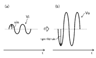
- the horizontal axis represents "Vip-Vin", which is the difference between the input signal Vip and the input signal Vin, and shows changes in the respective output signals Vop and Von.
- FIG. 4(a) shows changes in the differential input signal Vi along the time axis
- FIG. 4(b) shows changes in the differential output signal Vo along the time axis.
- the output common voltage Vcm of the differential output signal Vo is represented by the following equation (1).
- VDD is the power supply voltage of the differential amplifier 50
- Rd is the combined impedance of the output load circuit 560 or the combined impedance of the output load circuit 570
- Is is the current flowing through the tail current source (transistor 515).
- the fluctuation component vin of the differential input signal Vi (the voltage of the differential input signal Vi minus the DC component of the input signal) and the fluctuation component vout of the differential output signal Vo (the voltage value of the differential output signal Vo minus the output common voltage Vcm) is represented by the following equation (2).
- gm is the transfer conductance of the differential pair of transistors (N-type transistors 511 and 512).
- the voltage headroom Vh of the differential amplifier 50 is represented by the following equation (3).
- the voltage headroom Vh is the potential difference between the power supply voltage and the output common voltage Vcm, and is the voltage amplitude margin that allows the signal to be extracted without distortion as the differential output signal Vo. . Therefore, when the voltage headroom Vh becomes small and a sufficient voltage amplitude margin cannot be secured, problems such as distortion of the differential output signal Vo occur. For example, when the differential amplifier 50 is used for a high-speed interface, there is a possibility that the signal quality cannot be sufficiently secured for the standard, and the common adjustment circuit of the present disclosure is made to solve it. .
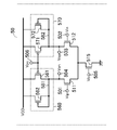
- FIG. 1 is a circuit diagram showing a configuration example of a common adjustment circuit according to the first embodiment.
- the common adjustment circuit 10 includes a reference voltage generation circuit 11 for generating the reference voltage Vrf, a second comparator 19, and a replica circuit 20.
- the reference voltage generation circuit 11 includes a first comparator 151 , a first transistor 111 , a first resistor 121 , a second resistor 122 and a current mirror circuit 161 .
- the first comparator 151 has one input to which the reference voltage Vid is applied via the input terminal 101 and the other input to which the source of the N-type first transistor 111 is connected via the first node 181 .
- the first comparator 151 compares the reference voltage Vid and the source voltage of the first transistor 111 and outputs the comparison result to the gate of the first transistor 111 . Accordingly, the voltage of the first node 181 is adjusted to the reference voltage Vid.
- the reference voltage Vid is supplied from a circuit that reduces voltage fluctuations due to fluctuations in the manufacturing process and changes in the usage environment such as power supply voltage fluctuations and temperature fluctuations.
- the reference voltage Vid is supplied, for example, from a conventionally known bandgap reference circuit.
- the first resistor 121 is provided between the first node 181 and the ground VSS (corresponding to the first power supply). As a result, a current I1 represented by the following equation (4) flows through the first transistor 111 .
- R1 is the resistance value of the first resistor 121.
- the current mirror circuit 161 includes a second P-type transistor 112 for passing the current I1 (hereinafter referred to as input current I1) as an input current, and a third P-type transistor 113 for passing an output current I2.
- the output current I2 can be adjusted, for example, by changing the size ratio of the second transistor 112 and the third transistor 113, or by changing the reference voltage Vid or the resistance value R1 of the first resistor 121.
- the gate and drain of the second transistor 112 are connected to the drain of the first transistor 111 via the second node 182 .
- the source of the second transistor 112 is connected to the power supply VDD (corresponding to the second power supply) via the third resistor 123 .
- a gate of the third transistor 113 is connected to the second node 182 . That is, the gates of the second transistor 112 and the third transistor 113 are connected to each other.
- the drain of the third transistor 113 is connected to ground VSS.
- a source of the third transistor 113 is connected to the power supply VDD through the second resistor 122 .
- a node connecting the source of the third transistor 113 and the second resistor 122 is called a "third node 183".
- a third node 183 is connected to one input of the second comparator 19 .
- one input of the second comparator 19 is supplied with the reference voltage Vrf given by the following equation (5).
- R2 is the resistance value of the second resistor 122.
- the second comparator 19 has one input to which the reference voltage Vrf is applied, and the other input to which the output node 282 (corresponding to the replica output node) of the replica circuit 20 is connected.
- the second comparator 19 compares the reference voltage Vrf and the output of the replica circuit 20 and outputs the comparison result to the node 281 .
- the node 281 is connected to the output terminal 102 and the gate of the replica transistor 261 of the replica circuit 20 which will be described later.
- the replica circuit 20 is a circuit that imitates the circuit configuration of the differential amplifier 50 to which the common adjustment circuit 10 is connected. That is, the replica circuit 20 is a circuit whose configuration changes according to the differential amplifier 50 to which the common adjustment circuit 10 is connected.
- FIG. 1 shows the replica circuit 20 when the common adjustment circuit 10 is connected to the differential amplifier 50 shown in FIG. 2 described above.
- the replica circuit 20 includes a replica load circuit 260 imitating the output load circuit 560 and a replica current source 215 imitating the transistor 515 operating as a tail current source.
- Replica load circuit 260 is configured to have the same electrical characteristics as output load circuit 560 .
- Replica current source 215 is configured to have half the current flowing through transistor 515 .
- the replica load circuit 260 includes P-type replica transistors 261 and 262 provided in parallel between the power supply VDD and the output node 282 .
- the gate of replica transistor 261 is connected to the output of second comparator 19 via node 281 . That is, the same voltage as the gate of the transistor 561 of the output load circuit 560 is applied to the gate of the replica transistor 261 .
- the drains of replica transistor 261 and replica transistor 262 are connected to the other input of second comparator 19 via output node 282 .
- the gate of replica transistor 262 is connected to output node 282 .
- Replica transistor 261 has the same electrical characteristics as transistor 561 and replica transistor 262 is configured to have the same electrical characteristics as transistor 562 .
- the voltage of the output node 282 of the replica circuit 20 is adjusted to the reference voltage Vrf.
- Replica circuit 20 output node 282 corresponds to the output node connected to output terminals 503 and 504 of differential amplifier 50 .
- the output common voltage Vcm at the output terminals 503 and 504 of the differential amplifier 50 is adjusted to the reference voltage Vrf.
- the output common voltage Vcm of the differential amplifier 50 is expressed by the following expression (6) from the above-described expression (5), and the voltage headroom Vh of the differential amplifier 50 is obtained from the expressions (6) and (3). , is represented by the following equation (7).
- the voltage headroom Vh does not depend on the power supply VDD, and the resistance ratio between the first resistor 121 and the second resistor 122 and the input It depends only on the current ratio between the current I1 and the output current I2.
- the resistance ratio between the first resistor 121 and the second resistor 122 is substantially unaffected by manufacturing variations.
- the current mirror circuit 161 is configured so as not to be substantially affected by fluctuations in the power supply voltage and temperature changes such as the temperature of the operating environment, so that highly accurate I2/I1 can be obtained. circuit.
- the reference voltage Vid can be substantially unaffected by fluctuations in the power supply voltage. Therefore, the common adjustment circuit 10 acts so that the voltage headroom Vh of the differential amplifier 50 does not fluctuate even if process variations and power supply voltage fluctuations occur, thereby solving the problem of the prior art. Details will be described in the following "Comparative Example".
- the common adjustment circuit 10 of the present embodiment can easily change the voltage headroom Vh by changing the mirror ratio I2/I1 and the resistance ratio R2/R1 of the current mirror circuit 161 .
- a common voltage generation circuit includes a load element (with a resistance value of Rx) and a constant current source (with a current value of Ix) between a power supply voltage and a ground potential. are provided in series, and the output thereof is output to the differential amplifier via the comparator. Then, the reference voltage Vx input to the comparator corresponding to the second comparator 19 of the present disclosure and the voltage headroom Vhx of the connected differential amplifier are given by the following equations (8) and (9).
- the resistance value Rx of the load element fluctuates under the influence of variations in the manufacturing process. This fluctuation causes the voltage headroom Vhx of the differential amplifier to be connected to fluctuate, and the operation of the circuit is disrupted. It may become unstable. Even if a transistor element is used as a resistor instead of a resistor element, it is similarly affected by variations in the manufacturing process, but the configuration of this embodiment is not affected by such power supply voltage fluctuations.
- Comparative Example 2 As shown in FIG. 11 of Patent Document 1, the common voltage generation circuit is composed of a resistance voltage dividing circuit with a resistance ratio of Ry1/Ry2, and outputs the output to a differential amplifier via a comparator. Configuration. Then, the reference voltage Vy input to the comparator corresponding to the second comparator 19 of the present disclosure and the voltage headroom Vhy of the connected differential amplifier are given by the following equations (10) and (11).
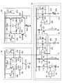
- FIG. 5 is a circuit diagram showing the configuration of a differential amplifier circuit including a common adjustment circuit 10 and a differential amplifier 60 according to Modification 1 of the first embodiment.
- FIG. 5 shows the configuration of a differential amplifier circuit including a common adjustment circuit 10 and a differential amplifier 60 according to Modification 1 of the first embodiment.
- the current mirror circuit 161 is a cascode type circuit. Specifically, in this modification, a fourth transistor 114 is provided between the second transistor 112 and the first transistor 111, and a fifth transistor 115 is provided between the third transistor 113 and the ground VSS. That is, the fourth transistor 114 and the fifth transistor 115 are cascode-connected to the second transistor 112 and the third transistor 113 .
- the precision of the mirror ratio of current mirror circuit 161 is further improved, and the precision of reference voltage Vrf (output common voltage Vcm) and voltage headroom Vh can be further improved.
- FIG. 5 shows an example in which the configuration of the differential amplifier 60 is different, so that the configuration of the replica circuit 20 is different from that in FIG.
- the differential amplifier of FIG. 5 is used, for example, as a continuous time linear equalizer for the front end of high speed interfaces.
- the differential amplifier circuit includes multiple differential amplifiers 60 having the same configuration and electrical characteristics.
- Each differential amplifier 60 amplifies a differential input signal Vi input from a pair of input terminals 601 and 602 and outputs from a pair of output terminals 603 and 604 as a differential output signal Vo.
- the differential amplifier 60 includes a differential pair of transistors (N-type transistors 611 and 612), a pair of output load circuits 640 and 650, a source load 660, and tail current sources 665 and 666.
- the source of transistor 611 is connected to ground VSS through tail current source 665 and the source of transistor 612 is connected to ground VSS through tail current source 666 .
- the source load 660 has a configuration in which a resistor 661 and a capacitor 662 are connected in parallel between the sources of the transistors 611 and 612 .
- transistors 611 and 612 and output load circuits 640 and 650 are configured to have the same electrical characteristics.
- tail current source 665 and tail current source 666 are configured to provide the same current.
- the output load circuit 640 corresponds to the output load circuit 560 in FIG. 2, and differs from FIG. 2 in that it is a parallel circuit of a P-type transistor 641 and a resistor 642. 5, a series-connected resistor 621 and a peaking inductor 631 are provided between the output load circuit 640 and the output terminal 603 .
- the output load circuit 650 corresponds to the output load circuit 570 in FIG. 2 and differs from FIG. 2 in that it is a parallel circuit of a P-type transistor 651 and a resistor 652 .
- a series-connected resistor 622 and a peaking inductor 632 are provided between the output load circuit 650 and the output terminal 604 .
- P-type transistor 641 and P-type transistor 651 have the same electrical characteristics, and resistors 642 and 652 are configured to have the same electrical characteristics. Furthermore, resistors 621 and 622 have the same electrical characteristics, and peaking inductors 631 and 632 are configured to have the same electrical characteristics.
- the replica circuit 20 differs from FIG. 1 in that it is a circuit configured to imitate the circuit configuration of the differential amplifier 60.
- the replica circuit 20 includes a replica load circuit 340 modeled on the output load circuit 640, a replica resistor 321 modeled on the resistor 621, a replica inductor 331 modeled on the peaking inductor 631, and a replica current source 365 modeled on the tail current source 665.
- the replica load circuit 340 is a parallel circuit of a replica transistor 341 imitating a P-type transistor 641 and a replica resistor 342 imitating a resistor 642 .
- Replica load circuit 340 is configured to have the same electrical characteristics as output load circuit 640 , i.e., replica transistor 341 has the same electrical characteristics as transistor 641 and replica resistor 342 has the same electrical characteristics as resistor 642 . be.
- Replica current source 365 is configured to carry the same current that flows through current source 665 .
- the output common voltage Vcm of the differential amplifier 60 is represented by the above-described formula (6)
- the voltage headroom Vh of the differential amplifier 60 is represented by the above-described formula (7). That is, by using the common adjustment circuit 10 of this modification, the voltage headroom Vh of the differential amplifier 60 does not depend on the power supply VDD, and the resistance ratio between the first resistor 121 and the second resistor 122 and the input current It depends only on the current ratio between I1 and the output current I2. As a result, the common adjustment circuit 10 acts so that the voltage headroom Vh of the differential amplifier 60 does not fluctuate even if process variations and power supply voltage fluctuations occur, thereby solving the problem of the prior art. Also, the voltage headroom Vh can be easily changed.
- the differential amplifier circuit according to this modification, a plurality of differential amplifiers 60 having the same configuration of the output load circuit 640 are provided, and the bias voltage Vpc is supplied from the common adjustment circuit 10 common to them. .
- the plurality of differential amplifiers 60 can be operated so that the voltage headroom Vh of the differential amplifiers 60 does not fluctuate even if process variations and power supply voltage fluctuations occur while suppressing an increase in area.
- a high gain can be obtained by cascade-connecting a plurality of stages of differential amplifiers 60.
- the configuration of this modified example can be preferably used.
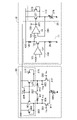
- FIG. 6 is a circuit diagram showing the configuration of a differential amplifier circuit including the common adjustment circuit 10 and differential amplifiers 60 and 70 according to Modification 2 of the first embodiment.
- FIG. 6 differences from the first modification (FIG. 5) described above will be mainly described, and descriptions of common configurations may be omitted.
- the differential amplifier circuit in FIG. 6 includes a plurality of differential amplifiers 60 and 70 with mutually different configurations.
- two differential amplifiers 60 and 70 are exemplified, and one differential amplifier 60 has the same configuration as that of Modification 1, but the number of differential amplifiers is not limited to two. may be a combination of different differential amplifiers.
- a third comparator 191 provided corresponding to the first replica circuit 201 and a third comparator provided corresponding to the first replica circuit 202 192.
- the third comparator 191 has one input connected to the third node 183 to receive the reference voltage Vrf, and the other input connected to the output node 282 (corresponding to the replica output node) of the first replica circuit 201 .
- the third comparator 191 compares the reference voltage Vrf and the output of the first replica circuit 201 and outputs the comparison result (bias voltage Vpc1) to the node 281 .
- the node 281 is connected to the output terminal 102 and the gate of the replica transistor 341 of the first replica circuit 201, which will be described later.
- Output terminal 102 is connected to input terminal 605 of differential amplifier 60 .
- Third comparator 191 applies bias voltage Vpc1 to the gates of transistor 641 and transistor 651, which will be described later.
- the third comparator 192 has one input connected to the third node 183 to receive the reference voltage Vrf, and the other input connected to the output node 284 (corresponding to the replica output node) of the first replica circuit 202 .
- Third comparator 192 compares reference voltage Vrf and the output of first replica circuit 202 and outputs the comparison result (bias voltage Vpc2) to node 283 .
- the node 283 is connected to the output terminal 103 and the gate of the replica transistor 441 of the first replica circuit 202, which will be described later.
- Output terminal 103 is connected to input terminal 705 of differential amplifier 70 .
- Third comparator 192 applies bias voltage Vpc2 to the gates of transistors 741 and 751 of differential amplifier 70 .
- the differential amplifier 70 amplifies the differential input signal Vi input from the paired input terminals 701 and 702 and outputs it from the paired output terminals 703 and 704 as the differential output signal Vo.
- the circuit configuration of the differential amplifier 70 is a configuration in which the peaking inductors 631 and 632 are omitted from the differential amplifier 60 .
- the differential amplifier 60 and the differential amplifier 70 correspond to those having the same last two digits, and the detailed description thereof is omitted here.
- transistors 711 and 712, output load circuits 740 and 750, and resistors 721 and 722 are configured to have the same electrical characteristics.
- tail current source 765 and tail current source 766 are configured to provide the same current.
- the replica circuit 20 includes a first replica circuit 201 configured to imitate the circuit configuration of the differential amplifier 60, and a first replica circuit 202 configured to imitate the circuit configuration of the differential amplifier 70. Prepare.
- the first replica circuit 201 has the same configuration as the replica circuit 20 in FIG.
- the first replica circuit 202 includes a replica load circuit 440 imitating the output load circuit 740 , a replica resistor 421 imitating the resistor 721 , and a replica current source 465 imitating the tail current source 765 .
- the replica load circuit 440 is a parallel circuit of a replica transistor 441 modeled on a P-type transistor 741 and a replica resistor 442 modeled on a resistor 742 .
- Replica load circuit 440 is configured to have the same electrical characteristics as output load circuit 740 , i.e., replica transistor 441 has the same electrical characteristics as transistor 741 and replica resistor 442 has the same electrical characteristics as resistor 742 . be done.
- replica resistor 421 is configured to have the same electrical characteristics as resistor 721 .
- Replica current source 465 is configured to carry the same current that flows through tail current source 765 .
- the output common voltage Vcm of the differential amplifier 60 and the output common voltage Vcm of the differential amplifier 70 are each represented by the above-described equation (6).
- the voltage headroom Vh of the differential amplifier 60 and the voltage headroom Vh of the differential amplifier 70 are each represented by the above equation (7).
- the common adjustment circuit 10 of this modification acts so that the voltage headroom Vh of the differential amplifier 60 does not fluctuate even if process variations and power supply voltage fluctuations occur, thereby solving the problem of the prior art. Also, the voltage headroom Vh can be easily changed. The same applies to the differential amplifier 70 as well.
- the voltage headroom Vh for each of the differential amplifiers 60 and 70 can be increased while suppressing the amount of circuit increase. It is possible to supply bias voltages Vpc1, Vpc2 which act to be stable.
- FIG. 7 is a circuit diagram showing the configuration of a differential amplifier circuit including a common adjustment circuit 10 and differential amplifiers 50 and 80 according to Modification 3 of the first embodiment.
- FIG. 7 shows differences from the above-described first embodiment (FIGS. 1 and 2), and descriptions of common configurations may be omitted.
- the configurations of differential amplifier 50 and common adjustment circuit 10 corresponding thereto are the same as in FIG. 1, and the configurations of differential amplifier 80 and common adjustment circuit 10 corresponding thereto will be described here.
- the gate of the sixth transistor 116 is connected to the second node 182, and the gates of the second transistor 112 are connected to each other.
- the output current I3 flows through the sixth transistor 116 .
- the output current I3 can be adjusted, for example, by changing the size ratio between the second transistor 112 and the sixth transistor 116, or by changing the reference voltage Vid or the resistance value R1 of the first resistor 121.
- the drain of the sixth transistor 116 is connected to the ground VSS.
- the source of sixth transistor 116 is connected to power supply VDD through fourth resistor 124 .
- a node connecting the source of the sixth transistor 116 and the fourth resistor 124 is called a "fifth node 185".
- a fifth node 185 is connected to one input of the third comparator 193 .
- one input of the third comparator 193 is supplied with the reference voltage Vrf2 given by the following equation (12).
- R4 is the resistance value of the fourth resistor 124.
- the third comparator 193 has one input to which the reference voltage Vrf2 is applied and the other input to which the output node 286 (corresponding to the replica output node) of the second replica circuit 203 is connected.
- Third comparator 193 compares reference voltage Vrf ⁇ b>2 with the output of second replica circuit 203 and outputs the comparison result to node 285 .
- the node 285 is connected to the output terminal 104 and the gate of the replica transistor 271 of the second replica circuit 203, which will be described later.
- Output terminal 104 is connected to input terminal 806 of differential amplifier 80 .
- Third comparator 193 applies bias voltage Vpc3 to the gates of transistors 861 and 871 of differential amplifier 80 .
- the differential amplifier 80 amplifies a differential input signal Vi2 (Vip2, Vin2) input from paired input terminals 801, 802, and outputs a differential output signal Vo2 (Vop2, Von2) from paired output terminals 803, 804. ).
- the circuit configuration of differential amplifier 80 is such that in addition to differential amplifier 50, a series circuit in which resistor 821, switch 822 and resistor 823 are connected in series is connected between output terminal 803 and output terminal 804. different. Also, a variable current source 866 is connected as a tail current source. By adding such a configuration, the gain can be changed without changing the common voltage Vcm, and the output amplitude can be changed without using the common adjustment circuit 10.
- differential amplifier 50 and the differential amplifier 80 correspond to those having the same last two digits, and the description of the corresponding configurations may be omitted here.
- differential amplifier 80 transistors 811 and 812, output load circuits 860 and 870, and resistors 821 and 823 are configured to have the same electrical characteristics.
- the second replica circuit 203 includes a replica load circuit 270 imitating the output load circuit 860 and a replica current source 276 imitating the variable current source 866 .
- the replica load circuit 270 is a parallel circuit of a replica transistor 271 imitating the P-type transistor 861 and a replica transistor 272 imitating the P-type transistor 862 .
- Replica load circuit 270 is configured to have the same electrical characteristics as output load circuit 860 , i.e., replica transistor 271 has the same electrical characteristics as transistor 861 and replica transistor 272 has the same electrical characteristics as transistor 862 . be done.
- Replica current source 276 is configured to draw half the current that flows through variable current source 866 .
- the output common voltage Vcm of the differential amplifier 80 is represented by the following equation (13), as in the above-described embodiment.
- the voltage headroom Vh of the differential amplifier 80 is represented by the above equation (14).
- the voltage headroom Vh of the differential amplifier 80 does not depend on the power supply VDD, and the first resistor 121 and the fourth resistor 124 and the current ratio between the input current I1 and the output current I3.
- the common adjustment circuit 10 acts so that the voltage headroom Vh of the differential amplifier 80 does not fluctuate even if process variations and power supply voltage fluctuations occur, thereby solving the problem of the prior art. Also, the voltage headroom Vh can be easily changed. The same is true for the differential amplifier 50 as well.
- the common adjustment circuit 10 that supplies the bias voltages Vpc and Vpc3 corresponding to the differential amplifiers 50 and 80 that are set to output common voltages different from each other is realized while suppressing an increase in circuit scale. be able to.
- FIG. 8 is a circuit diagram showing a configuration example of a common adjustment circuit according to the second embodiment.
- the common adjustment circuit 10 includes a reference voltage generation circuit 11 for generating the reference voltage Vrf, a second comparator 19, and a replica circuit 20.
- a differential amplifier an example using the differential amplifier 80 described in the above-mentioned "Modification 3 of the first embodiment (FIG. 7)" is shown. Therefore, the replica circuit 20 in FIG. 8 has the same configuration as the second replica circuit 203 in FIG. In this embodiment, the differential amplifiers 50, 60 and 70 may be used, in which case the configuration of the replica circuit 20 is different.
- the reference voltage generation circuit 11 includes a first comparator 152 , a first transistor 118 , a first resistor 128 and a second resistor 129 .
- the first comparator 152 has one input to which the reference voltage Vid is applied via the input terminal 101 and the other input to which the drain of the first P-type transistor 118 is connected via the first node 188 .
- the first comparator 152 compares the reference voltage Vid with the drain voltage of the first transistor 118 and outputs the comparison result to the gate of the first transistor 118 . Thereby, the voltage of the first node 188 is adjusted to the reference voltage Vid.
- the reference voltage Vid is supplied from a circuit (for example, a bandgap reference circuit) that reduces voltage fluctuations due to variations in the manufacturing process and changes in the operating environment such as power supply voltage fluctuations and temperature fluctuations. be done.
- the first resistor 128 is provided between the first node 181 and the ground VSS (corresponding to the first power supply). As a result, the current I ⁇ b>1 represented by the above equation (4) flows through the first transistor 111 .
- R1 is the resistance value of the first resistor 128.
- the source of the first transistor 118 is connected through the second resistor 129 to the power supply VDD.
- the node connecting the source of the first transistor 118 and the second resistor 129 is referred to as a "second node 189".
- a second node 189 is connected to one input of the second comparator 19 .
- one input of the second comparator 19 is supplied with the reference voltage Vrf given by the following equation (15).
- R2 is the resistance value of the second resistor 129.
- the second comparator 19 has one input to which the reference voltage Vrf is applied and the other input to which the output node 286 (corresponding to the replica output node) of the replica circuit 20 is connected. Second comparator 19 compares reference voltage Vrf with the output of replica circuit 20 and outputs the comparison result to node 285 . Output terminal 108 and the gate of replica transistor 271 of replica circuit 20 are connected to node 285 . As described above, the voltage at output node 286 of replica circuit 20 is regulated to reference voltage Vrf.
- the output common voltage Vcm of the differential amplifier 80 is expressed by the following equation (16), and from the equations (16) and (3), the voltage headroom Vh of the differential amplifier 80 is , is represented by the following equation (17).
- the voltage headroom Vh of the differential amplifier 80 does not depend on the power supply VDD, and the resistance ratio between the first resistor 128 and the second resistor 129 is A common regulating circuit 10 is implemented that acts only in dependence on Furthermore, the voltage headroom Vh can be set with fewer parameters than in the first embodiment.
- FIG. 9 shows an example in which the differential amplifier connected with the common adjustment circuit according to the above embodiment is used in a continuous-time linear equalizer 94 of an analog front end (receiving circuit) of a high-speed interface device.
- data output from the transmission circuit 91 of the high-speed interface is input to a continuous-time linear equalizer 94 via a cable 92 and a termination circuit 93 of the reception circuit.
- the continuous-time linear equalizer 94 has, for example, a configuration in which the differential amplifier 60 shown in FIG. 5, the differential amplifier 80 shown in FIG. 8, and the differential amplifier 10 shown in FIG. 2 are connected in cascade.
- the differential amplifier 60 restores the attenuated gain.
- the differential amplifier 80 adjusts the amplitude of the gain-adjusted data to the input range of the decision feedback equalizer 95 in the subsequent stage.
- the common adjustment circuit 10 described above is connected to each of the differential amplifiers 60, 80 and 50.
- the applications of the differential amplifiers 50, 60, 70, 80 and the common adjustment circuit 10 are not limited to high-speed interfaces. Further, as described in modifications 1, 2, etc., the bias voltage Vpc is supplied to the plurality of differential amplifiers 50, 60, 70, 80 by the common adjustment circuit 10, which is smaller in number than the differential amplifiers. can be
- the common adjustment circuit of the present disclosure is extremely useful because it acts so that the voltage headroom of the differential amplifier does not fluctuate even with process variations and power supply voltage fluctuations.
- Second comparator 20 Replica circuit 50 Differential amplifier 60 Differential amplifier 70 Differential amplifier 80 Differential amplifier 111 First transistor 112 Second transistor 113 Third transistor 114 Fourth transistor 115 Fifth transistor 116 Sixth Transistor 118 First transistor 121 First resistor 122 Second resistor 123 Third resistor 124 Third resistor 128 First resistor 129 Second resistor 151 First comparator 152 First comparator 161 Current mirror circuit 181 First node 182 Second node 183 Third node 185 Fifth node 188 First node 189 Second node 193 Third comparator 203 Second replica circuit 261 Replica transistor 271 Replica transistor 282 Output node (replica output node) 286 output node (replica output node) 561, 571 Output load transistors 641, 651 Output load transistors 741, 751 Output load transistors 861, 871 Output load transistors VDD Power supply (second power supply) VSS ground (1st power supply)
Landscapes
- Engineering & Computer Science (AREA)
- Power Engineering (AREA)
- Amplifiers (AREA)
Priority Applications (3)
| Application Number | Priority Date | Filing Date | Title |
|---|---|---|---|
| PCT/JP2021/003553 WO2022162943A1 (ja) | 2021-02-01 | 2021-02-01 | コモン調整回路 |
| JP2022578008A JP7705052B2 (ja) | 2021-02-01 | 2021-02-01 | コモン調整回路 |
| US18/344,482 US20230361735A1 (en) | 2021-02-01 | 2023-06-29 | Common adjustment circuit |
Applications Claiming Priority (1)
| Application Number | Priority Date | Filing Date | Title |
|---|---|---|---|
| PCT/JP2021/003553 WO2022162943A1 (ja) | 2021-02-01 | 2021-02-01 | コモン調整回路 |
Related Child Applications (1)
| Application Number | Title | Priority Date | Filing Date |
|---|---|---|---|
| US18/344,482 Continuation US20230361735A1 (en) | 2021-02-01 | 2023-06-29 | Common adjustment circuit |
Publications (1)
| Publication Number | Publication Date |
|---|---|
| WO2022162943A1 true WO2022162943A1 (ja) | 2022-08-04 |
Family
ID=82653079
Family Applications (1)
| Application Number | Title | Priority Date | Filing Date |
|---|---|---|---|
| PCT/JP2021/003553 Ceased WO2022162943A1 (ja) | 2021-02-01 | 2021-02-01 | コモン調整回路 |
Country Status (3)
| Country | Link |
|---|---|
| US (1) | US20230361735A1 (https=) |
| JP (1) | JP7705052B2 (https=) |
| WO (1) | WO2022162943A1 (https=) |
Cited By (1)
| Publication number | Priority date | Publication date | Assignee | Title |
|---|---|---|---|---|
| CN115426000A (zh) * | 2022-08-31 | 2022-12-02 | 集益威半导体(上海)有限公司 | 模拟接收前端电路 |
Families Citing this family (1)
| Publication number | Priority date | Publication date | Assignee | Title |
|---|---|---|---|---|
| US11977402B2 (en) * | 2021-11-29 | 2024-05-07 | Texas Instruments Incorporated | Transconductors with improved slew performance and low quiescent current |
Citations (4)
| Publication number | Priority date | Publication date | Assignee | Title |
|---|---|---|---|---|
| US20020190782A1 (en) * | 2001-06-14 | 2002-12-19 | Somerville Thomas A. | Circuit with source follower output stage and adaptive current mirror bias |
| JP2008306504A (ja) * | 2007-06-08 | 2008-12-18 | Renesas Technology Corp | 差動増幅回路及びa/d変換器 |
| US9007098B1 (en) * | 2013-03-01 | 2015-04-14 | Iml International | Current mode DVR or PVCOM with integrated resistors |
| JP2020509649A (ja) * | 2017-03-14 | 2020-03-26 | ホアウェイ・テクノロジーズ・カンパニー・リミテッド | 線形バーストモードトランスインピーダンス増幅器における閉ループ自動利得制御 |
Family Cites Families (4)
| Publication number | Priority date | Publication date | Assignee | Title |
|---|---|---|---|---|
| JP4683468B2 (ja) | 2005-03-22 | 2011-05-18 | ルネサスエレクトロニクス株式会社 | 高周波電力増幅回路 |
| JP2008067188A (ja) | 2006-09-08 | 2008-03-21 | Ricoh Co Ltd | 差動増幅回路及びその差動増幅回路を使用した充電制御装置 |
| JP5829138B2 (ja) | 2012-01-31 | 2015-12-09 | ローム株式会社 | 差動増幅器、それを用いた電流ドライバ、発光装置および電子機器 |
| JP2013207453A (ja) | 2012-03-28 | 2013-10-07 | Renesas Electronics Corp | 増幅回路 |
-
2021
- 2021-02-01 JP JP2022578008A patent/JP7705052B2/ja active Active
- 2021-02-01 WO PCT/JP2021/003553 patent/WO2022162943A1/ja not_active Ceased
-
2023
- 2023-06-29 US US18/344,482 patent/US20230361735A1/en active Pending
Patent Citations (4)
| Publication number | Priority date | Publication date | Assignee | Title |
|---|---|---|---|---|
| US20020190782A1 (en) * | 2001-06-14 | 2002-12-19 | Somerville Thomas A. | Circuit with source follower output stage and adaptive current mirror bias |
| JP2008306504A (ja) * | 2007-06-08 | 2008-12-18 | Renesas Technology Corp | 差動増幅回路及びa/d変換器 |
| US9007098B1 (en) * | 2013-03-01 | 2015-04-14 | Iml International | Current mode DVR or PVCOM with integrated resistors |
| JP2020509649A (ja) * | 2017-03-14 | 2020-03-26 | ホアウェイ・テクノロジーズ・カンパニー・リミテッド | 線形バーストモードトランスインピーダンス増幅器における閉ループ自動利得制御 |
Cited By (2)
| Publication number | Priority date | Publication date | Assignee | Title |
|---|---|---|---|---|
| CN115426000A (zh) * | 2022-08-31 | 2022-12-02 | 集益威半导体(上海)有限公司 | 模拟接收前端电路 |
| CN115426000B (zh) * | 2022-08-31 | 2023-07-04 | 集益威半导体(上海)有限公司 | 模拟接收前端电路 |
Also Published As
| Publication number | Publication date |
|---|---|
| JP7705052B2 (ja) | 2025-07-09 |
| US20230361735A1 (en) | 2023-11-09 |
| JPWO2022162943A1 (https=) | 2022-08-04 |
Similar Documents
| Publication | Publication Date | Title |
|---|---|---|
| KR100377064B1 (ko) | 적응바이어서회로및공통모드궤환회로를갖는완전차동폴디드캐스코드씨모오스(cmos)오피앰프(opamp)회로 | |
| Carrillo et al. | Constant-g/sub m/constant-slew-rate high-bandwidth low-voltage rail-to-rail CMOS input stage for VLSI cell libraries | |
| JP5012412B2 (ja) | 増幅装置及びバイアス回路 | |
| US20080238546A1 (en) | Fully differential class ab amplifier and amplifying method using single-ended, two-stage amplifier | |
| US5789981A (en) | High-gain operational transconductance amplifier offering improved bandwidth | |
| JP5092687B2 (ja) | 増幅装置及びGm補償バイアス回路 | |
| CN110690878B (zh) | 比较器中折叠共源共栅级的输出的偏置方法和对应比较器 | |
| CN1262811A (zh) | 高速和高增益运算放大器 | |
| US20230361735A1 (en) | Common adjustment circuit | |
| US8169263B2 (en) | Differential gm-boosting circuit and applications | |
| CN101881984B (zh) | 基准信号产生器及其方法和系统 | |
| US8570099B2 (en) | Single-ended-to-differential filter using common mode feedback | |
| Kumar | Flexible and high throughput designs of operational amplifiers | |
| US8179194B2 (en) | System and method for a reference generator | |
| JP6132881B2 (ja) | 電圧可変利得増幅回路及び差動入力電圧の増幅方法 | |
| US7859339B2 (en) | Differential amplification circuit | |
| Nischal et al. | Study of a self biased high swing cascode current mirror based folded cascode operational amplifier | |
| CN107786185B (zh) | 相位内插器 | |
| JPWO2022162943A5 (https=) | ||
| JP5788739B2 (ja) | 電圧可変利得増幅回路 | |
| Yan et al. | Continuous-time common-mode feedback circuit for applications with large output swing and high output impedance | |
| CN113853743B (zh) | 输出极补偿的运算放大器 | |
| JP4682419B2 (ja) | 可変利得増幅回路 | |
| US7532045B1 (en) | Low-complexity active transconductance circuit | |
| US6831501B1 (en) | Common-mode controlled differential gain boosting |
Legal Events
| Date | Code | Title | Description |
|---|---|---|---|
| 121 | Ep: the epo has been informed by wipo that ep was designated in this application |
Ref document number: 21922953 Country of ref document: EP Kind code of ref document: A1 |
|
| ENP | Entry into the national phase |
Ref document number: 2022578008 Country of ref document: JP Kind code of ref document: A |
|
| NENP | Non-entry into the national phase |
Ref country code: DE |
|
| 122 | Ep: pct application non-entry in european phase |
Ref document number: 21922953 Country of ref document: EP Kind code of ref document: A1 |