WO2022158563A1 - Procédé de jonction, dispositif de jonction, et système de jonction - Google Patents
Procédé de jonction, dispositif de jonction, et système de jonction Download PDFInfo
- Publication number
- WO2022158563A1 WO2022158563A1 PCT/JP2022/002175 JP2022002175W WO2022158563A1 WO 2022158563 A1 WO2022158563 A1 WO 2022158563A1 JP 2022002175 W JP2022002175 W JP 2022002175W WO 2022158563 A1 WO2022158563 A1 WO 2022158563A1
- Authority
- WO
- WIPO (PCT)
- Prior art keywords
- bonding
- bonded
- objects
- substrates
- chamber
- Prior art date
Links
- 238000000034 method Methods 0.000 title claims abstract description 210
- 238000005304 joining Methods 0.000 title claims abstract description 106
- 239000000758 substrate Substances 0.000 claims abstract description 764
- 238000010438 heat treatment Methods 0.000 claims abstract description 268
- 239000012298 atmosphere Substances 0.000 claims abstract description 91
- 230000004913 activation Effects 0.000 claims abstract description 88
- 238000011282 treatment Methods 0.000 claims abstract description 65
- 230000003213 activating effect Effects 0.000 claims abstract description 15
- 238000001994 activation Methods 0.000 claims description 121
- 239000002245 particle Substances 0.000 claims description 117
- XLYOFNOQVPJJNP-UHFFFAOYSA-N water Substances O XLYOFNOQVPJJNP-UHFFFAOYSA-N 0.000 claims description 93
- 238000004140 cleaning Methods 0.000 claims description 82
- 238000012545 processing Methods 0.000 claims description 52
- 239000011856 silicon-based particle Substances 0.000 claims description 45
- 230000007246 mechanism Effects 0.000 claims description 32
- GQYHUHYESMUTHG-UHFFFAOYSA-N lithium niobate Chemical compound [Li+].[O-][Nb](=O)=O GQYHUHYESMUTHG-UHFFFAOYSA-N 0.000 claims description 24
- WSMQKESQZFQMFW-UHFFFAOYSA-N 5-methyl-pyrazole-3-carboxylic acid Chemical compound CC1=CC(C(O)=O)=NN1 WSMQKESQZFQMFW-UHFFFAOYSA-N 0.000 claims description 23
- 230000001678 irradiating effect Effects 0.000 claims description 21
- 239000010408 film Substances 0.000 claims description 18
- 238000000151 deposition Methods 0.000 claims description 11
- 238000005406 washing Methods 0.000 claims description 11
- 150000004767 nitrides Chemical class 0.000 claims description 9
- 238000001816 cooling Methods 0.000 claims description 8
- 150000002500 ions Chemical class 0.000 claims description 8
- 230000003287 optical effect Effects 0.000 claims description 8
- 229910052751 metal Inorganic materials 0.000 claims description 7
- 239000002184 metal Substances 0.000 claims description 7
- 238000013459 approach Methods 0.000 claims description 6
- 238000011156 evaluation Methods 0.000 claims description 6
- 229910003327 LiNbO3 Inorganic materials 0.000 claims description 5
- 229910012463 LiTaO3 Inorganic materials 0.000 claims description 5
- 230000008021 deposition Effects 0.000 claims description 5
- 239000011521 glass Substances 0.000 claims description 4
- 238000005468 ion implantation Methods 0.000 claims description 4
- 239000010409 thin film Substances 0.000 claims description 3
- 238000003466 welding Methods 0.000 claims 1
- 230000008569 process Effects 0.000 description 101
- 230000032258 transport Effects 0.000 description 69
- 238000012546 transfer Methods 0.000 description 57
- 239000012535 impurity Substances 0.000 description 53
- 239000007789 gas Substances 0.000 description 25
- 229910013641 LiNbO 3 Inorganic materials 0.000 description 19
- 230000002093 peripheral effect Effects 0.000 description 19
- 238000010586 diagram Methods 0.000 description 18
- 230000004048 modification Effects 0.000 description 18
- 238000012986 modification Methods 0.000 description 18
- VYPSYNLAJGMNEJ-UHFFFAOYSA-N Silicium dioxide Chemical compound O=[Si]=O VYPSYNLAJGMNEJ-UHFFFAOYSA-N 0.000 description 17
- XKRFYHLGVUSROY-UHFFFAOYSA-N Argon Chemical compound [Ar] XKRFYHLGVUSROY-UHFFFAOYSA-N 0.000 description 16
- 230000000694 effects Effects 0.000 description 14
- 238000005260 corrosion Methods 0.000 description 12
- 230000007797 corrosion Effects 0.000 description 12
- 230000001965 increasing effect Effects 0.000 description 12
- 239000013077 target material Substances 0.000 description 12
- 238000006073 displacement reaction Methods 0.000 description 10
- 125000002887 hydroxy group Chemical group [H]O* 0.000 description 10
- 230000006698 induction Effects 0.000 description 10
- 229910052786 argon Inorganic materials 0.000 description 9
- IJGRMHOSHXDMSA-UHFFFAOYSA-N Atomic nitrogen Chemical compound N#N IJGRMHOSHXDMSA-UHFFFAOYSA-N 0.000 description 8
- 101100095908 Chlamydomonas reinhardtii SLT3 gene Proteins 0.000 description 8
- 101000671638 Homo sapiens Vesicle transport protein USE1 Proteins 0.000 description 8
- 102100040106 Vesicle transport protein USE1 Human genes 0.000 description 8
- 229910052681 coesite Inorganic materials 0.000 description 8
- 229910052906 cristobalite Inorganic materials 0.000 description 8
- 229910001873 dinitrogen Inorganic materials 0.000 description 8
- 229910052682 stishovite Inorganic materials 0.000 description 8
- 229910052905 tridymite Inorganic materials 0.000 description 8
- MYMOFIZGZYHOMD-UHFFFAOYSA-N Dioxygen Chemical compound O=O MYMOFIZGZYHOMD-UHFFFAOYSA-N 0.000 description 7
- 101150104869 SLT2 gene Proteins 0.000 description 7
- 229910052581 Si3N4 Inorganic materials 0.000 description 7
- 238000005336 cracking Methods 0.000 description 7
- 229910001882 dioxygen Inorganic materials 0.000 description 7
- 239000000377 silicon dioxide Substances 0.000 description 7
- 235000012239 silicon dioxide Nutrition 0.000 description 7
- HQVNEWCFYHHQES-UHFFFAOYSA-N silicon nitride Chemical compound N12[Si]34N5[Si]62N3[Si]51N64 HQVNEWCFYHHQES-UHFFFAOYSA-N 0.000 description 7
- 238000005516 engineering process Methods 0.000 description 6
- 238000000605 extraction Methods 0.000 description 6
- 238000007667 floating Methods 0.000 description 6
- 229910052594 sapphire Inorganic materials 0.000 description 6
- 239000010980 sapphire Substances 0.000 description 6
- 229910004298 SiO 2 Inorganic materials 0.000 description 5
- 238000005530 etching Methods 0.000 description 5
- 230000006872 improvement Effects 0.000 description 5
- 238000011068 loading method Methods 0.000 description 5
- 239000000463 material Substances 0.000 description 5
- 238000005259 measurement Methods 0.000 description 5
- 238000001020 plasma etching Methods 0.000 description 5
- 230000003247 decreasing effect Effects 0.000 description 4
- 238000009792 diffusion process Methods 0.000 description 4
- PNEYBMLMFCGWSK-UHFFFAOYSA-N aluminium oxide Inorganic materials [O-2].[O-2].[O-2].[Al+3].[Al+3] PNEYBMLMFCGWSK-UHFFFAOYSA-N 0.000 description 3
- 238000000137 annealing Methods 0.000 description 3
- -1 argon ions Chemical class 0.000 description 3
- 239000003575 carbonaceous material Substances 0.000 description 3
- 229910052802 copper Inorganic materials 0.000 description 3
- 239000013078 crystal Substances 0.000 description 3
- 238000010304 firing Methods 0.000 description 3
- 229910052737 gold Inorganic materials 0.000 description 3
- 238000003780 insertion Methods 0.000 description 3
- 230000037431 insertion Effects 0.000 description 3
- 238000004519 manufacturing process Methods 0.000 description 3
- 239000012299 nitrogen atmosphere Substances 0.000 description 3
- PIGFYZPCRLYGLF-UHFFFAOYSA-N Aluminum nitride Chemical compound [Al]#N PIGFYZPCRLYGLF-UHFFFAOYSA-N 0.000 description 2
- OKTJSMMVPCPJKN-UHFFFAOYSA-N Carbon Chemical compound [C] OKTJSMMVPCPJKN-UHFFFAOYSA-N 0.000 description 2
- KRHYYFGTRYWZRS-UHFFFAOYSA-N Fluorane Chemical compound F KRHYYFGTRYWZRS-UHFFFAOYSA-N 0.000 description 2
- 229910001218 Gallium arsenide Inorganic materials 0.000 description 2
- JMASRVWKEDWRBT-UHFFFAOYSA-N Gallium nitride Chemical compound [Ga]#N JMASRVWKEDWRBT-UHFFFAOYSA-N 0.000 description 2
- 229910052782 aluminium Inorganic materials 0.000 description 2
- 125000004429 atom Chemical group 0.000 description 2
- 229910052799 carbon Inorganic materials 0.000 description 2
- 230000008859 change Effects 0.000 description 2
- 238000006243 chemical reaction Methods 0.000 description 2
- 239000004020 conductor Substances 0.000 description 2
- 238000012790 confirmation Methods 0.000 description 2
- 239000010432 diamond Substances 0.000 description 2
- 229910003460 diamond Inorganic materials 0.000 description 2
- AJNVQOSZGJRYEI-UHFFFAOYSA-N digallium;oxygen(2-) Chemical compound [O-2].[O-2].[O-2].[Ga+3].[Ga+3] AJNVQOSZGJRYEI-UHFFFAOYSA-N 0.000 description 2
- 239000007788 liquid Substances 0.000 description 2
- QJGQUHMNIGDVPM-UHFFFAOYSA-N nitrogen group Chemical group [N] QJGQUHMNIGDVPM-UHFFFAOYSA-N 0.000 description 2
- 230000000149 penetrating effect Effects 0.000 description 2
- 238000000926 separation method Methods 0.000 description 2
- HBMJWWWQQXIZIP-UHFFFAOYSA-N silicon carbide Chemical compound [Si+]#[C-] HBMJWWWQQXIZIP-UHFFFAOYSA-N 0.000 description 2
- 238000005507 spraying Methods 0.000 description 2
- 238000004544 sputter deposition Methods 0.000 description 2
- 239000000126 substance Substances 0.000 description 2
- 229910018072 Al 2 O 3 Inorganic materials 0.000 description 1
- 229910008045 Si-Si Inorganic materials 0.000 description 1
- 229910006411 Si—Si Inorganic materials 0.000 description 1
- 239000002253 acid Substances 0.000 description 1
- 230000008901 benefit Effects 0.000 description 1
- 238000004364 calculation method Methods 0.000 description 1
- 230000000052 comparative effect Effects 0.000 description 1
- 230000000295 complement effect Effects 0.000 description 1
- 229910052593 corundum Inorganic materials 0.000 description 1
- 238000005137 deposition process Methods 0.000 description 1
- 238000007599 discharging Methods 0.000 description 1
- 230000002708 enhancing effect Effects 0.000 description 1
- 125000004435 hydrogen atom Chemical group [H]* 0.000 description 1
- 239000007943 implant Substances 0.000 description 1
- 238000009616 inductively coupled plasma Methods 0.000 description 1
- 238000012966 insertion method Methods 0.000 description 1
- 239000012212 insulator Substances 0.000 description 1
- 238000005040 ion trap Methods 0.000 description 1
- 230000015654 memory Effects 0.000 description 1
- 229910021421 monocrystalline silicon Inorganic materials 0.000 description 1
- 230000007935 neutral effect Effects 0.000 description 1
- 239000003960 organic solvent Substances 0.000 description 1
- 238000003825 pressing Methods 0.000 description 1
- 230000005855 radiation Effects 0.000 description 1
- 230000009467 reduction Effects 0.000 description 1
- 229910052710 silicon Inorganic materials 0.000 description 1
- 239000010703 silicon Substances 0.000 description 1
- 229910052814 silicon oxide Inorganic materials 0.000 description 1
- 230000002459 sustained effect Effects 0.000 description 1
- 230000036962 time dependent Effects 0.000 description 1
- 235000012431 wafers Nutrition 0.000 description 1
- 229910001845 yogo sapphire Inorganic materials 0.000 description 1
Images


Classifications
-
- H—ELECTRICITY
- H01—ELECTRIC ELEMENTS
- H01L—SEMICONDUCTOR DEVICES NOT COVERED BY CLASS H10
- H01L21/00—Processes or apparatus adapted for the manufacture or treatment of semiconductor or solid state devices or of parts thereof
- H01L21/02—Manufacture or treatment of semiconductor devices or of parts thereof
- H01L21/04—Manufacture or treatment of semiconductor devices or of parts thereof the devices having potential barriers, e.g. a PN junction, depletion layer or carrier concentration layer
- H01L21/18—Manufacture or treatment of semiconductor devices or of parts thereof the devices having potential barriers, e.g. a PN junction, depletion layer or carrier concentration layer the devices having semiconductor bodies comprising elements of Group IV of the Periodic Table or AIIIBV compounds with or without impurities, e.g. doping materials
- H01L21/185—Joining of semiconductor bodies for junction formation
- H01L21/187—Joining of semiconductor bodies for junction formation by direct bonding
-
- B—PERFORMING OPERATIONS; TRANSPORTING
- B23—MACHINE TOOLS; METAL-WORKING NOT OTHERWISE PROVIDED FOR
- B23K—SOLDERING OR UNSOLDERING; WELDING; CLADDING OR PLATING BY SOLDERING OR WELDING; CUTTING BY APPLYING HEAT LOCALLY, e.g. FLAME CUTTING; WORKING BY LASER BEAM
- B23K20/00—Non-electric welding by applying impact or other pressure, with or without the application of heat, e.g. cladding or plating
- B23K20/24—Preliminary treatment
-
- B—PERFORMING OPERATIONS; TRANSPORTING
- B23—MACHINE TOOLS; METAL-WORKING NOT OTHERWISE PROVIDED FOR
- B23K—SOLDERING OR UNSOLDERING; WELDING; CLADDING OR PLATING BY SOLDERING OR WELDING; CUTTING BY APPLYING HEAT LOCALLY, e.g. FLAME CUTTING; WORKING BY LASER BEAM
- B23K20/00—Non-electric welding by applying impact or other pressure, with or without the application of heat, e.g. cladding or plating
- B23K20/008—Non-electric welding by applying impact or other pressure, with or without the application of heat, e.g. cladding or plating pressure combined with radiant energy
-
- B—PERFORMING OPERATIONS; TRANSPORTING
- B23—MACHINE TOOLS; METAL-WORKING NOT OTHERWISE PROVIDED FOR
- B23K—SOLDERING OR UNSOLDERING; WELDING; CLADDING OR PLATING BY SOLDERING OR WELDING; CUTTING BY APPLYING HEAT LOCALLY, e.g. FLAME CUTTING; WORKING BY LASER BEAM
- B23K20/00—Non-electric welding by applying impact or other pressure, with or without the application of heat, e.g. cladding or plating
- B23K20/02—Non-electric welding by applying impact or other pressure, with or without the application of heat, e.g. cladding or plating by means of a press ; Diffusion bonding
- B23K20/023—Thermo-compression bonding
-
- C—CHEMISTRY; METALLURGY
- C03—GLASS; MINERAL OR SLAG WOOL
- C03C—CHEMICAL COMPOSITION OF GLASSES, GLAZES OR VITREOUS ENAMELS; SURFACE TREATMENT OF GLASS; SURFACE TREATMENT OF FIBRES OR FILAMENTS MADE FROM GLASS, MINERALS OR SLAGS; JOINING GLASS TO GLASS OR OTHER MATERIALS
- C03C23/00—Other surface treatment of glass not in the form of fibres or filaments
- C03C23/0005—Other surface treatment of glass not in the form of fibres or filaments by irradiation
- C03C23/006—Other surface treatment of glass not in the form of fibres or filaments by irradiation by plasma or corona discharge
-
- C—CHEMISTRY; METALLURGY
- C03—GLASS; MINERAL OR SLAG WOOL
- C03C—CHEMICAL COMPOSITION OF GLASSES, GLAZES OR VITREOUS ENAMELS; SURFACE TREATMENT OF GLASS; SURFACE TREATMENT OF FIBRES OR FILAMENTS MADE FROM GLASS, MINERALS OR SLAGS; JOINING GLASS TO GLASS OR OTHER MATERIALS
- C03C23/00—Other surface treatment of glass not in the form of fibres or filaments
- C03C23/0075—Cleaning of glass
-
- C—CHEMISTRY; METALLURGY
- C03—GLASS; MINERAL OR SLAG WOOL
- C03C—CHEMICAL COMPOSITION OF GLASSES, GLAZES OR VITREOUS ENAMELS; SURFACE TREATMENT OF GLASS; SURFACE TREATMENT OF FIBRES OR FILAMENTS MADE FROM GLASS, MINERALS OR SLAGS; JOINING GLASS TO GLASS OR OTHER MATERIALS
- C03C27/00—Joining pieces of glass to pieces of other inorganic material; Joining glass to glass other than by fusing
- C03C27/06—Joining glass to glass by processes other than fusing
-
- H—ELECTRICITY
- H01—ELECTRIC ELEMENTS
- H01L—SEMICONDUCTOR DEVICES NOT COVERED BY CLASS H10
- H01L21/00—Processes or apparatus adapted for the manufacture or treatment of semiconductor or solid state devices or of parts thereof
- H01L21/02—Manufacture or treatment of semiconductor devices or of parts thereof
- H01L21/02002—Preparing wafers
-
- H—ELECTRICITY
- H01—ELECTRIC ELEMENTS
- H01L—SEMICONDUCTOR DEVICES NOT COVERED BY CLASS H10
- H01L21/00—Processes or apparatus adapted for the manufacture or treatment of semiconductor or solid state devices or of parts thereof
- H01L21/02—Manufacture or treatment of semiconductor devices or of parts thereof
- H01L21/04—Manufacture or treatment of semiconductor devices or of parts thereof the devices having potential barriers, e.g. a PN junction, depletion layer or carrier concentration layer
- H01L21/18—Manufacture or treatment of semiconductor devices or of parts thereof the devices having potential barriers, e.g. a PN junction, depletion layer or carrier concentration layer the devices having semiconductor bodies comprising elements of Group IV of the Periodic Table or AIIIBV compounds with or without impurities, e.g. doping materials
- H01L21/20—Deposition of semiconductor materials on a substrate, e.g. epitaxial growth solid phase epitaxy
- H01L21/2003—Deposition of semiconductor materials on a substrate, e.g. epitaxial growth solid phase epitaxy characterised by the substrate
- H01L21/2007—Bonding of semiconductor wafers to insulating substrates or to semiconducting substrates using an intermediate insulating layer
-
- H—ELECTRICITY
- H01—ELECTRIC ELEMENTS
- H01L—SEMICONDUCTOR DEVICES NOT COVERED BY CLASS H10
- H01L21/00—Processes or apparatus adapted for the manufacture or treatment of semiconductor or solid state devices or of parts thereof
- H01L21/67—Apparatus specially adapted for handling semiconductor or electric solid state devices during manufacture or treatment thereof; Apparatus specially adapted for handling wafers during manufacture or treatment of semiconductor or electric solid state devices or components ; Apparatus not specifically provided for elsewhere
- H01L21/67005—Apparatus not specifically provided for elsewhere
- H01L21/67011—Apparatus for manufacture or treatment
- H01L21/67092—Apparatus for mechanical treatment
-
- H—ELECTRICITY
- H01—ELECTRIC ELEMENTS
- H01L—SEMICONDUCTOR DEVICES NOT COVERED BY CLASS H10
- H01L21/00—Processes or apparatus adapted for the manufacture or treatment of semiconductor or solid state devices or of parts thereof
- H01L21/67—Apparatus specially adapted for handling semiconductor or electric solid state devices during manufacture or treatment thereof; Apparatus specially adapted for handling wafers during manufacture or treatment of semiconductor or electric solid state devices or components ; Apparatus not specifically provided for elsewhere
- H01L21/67005—Apparatus not specifically provided for elsewhere
- H01L21/67011—Apparatus for manufacture or treatment
- H01L21/67098—Apparatus for thermal treatment
- H01L21/67115—Apparatus for thermal treatment mainly by radiation
-
- H—ELECTRICITY
- H01—ELECTRIC ELEMENTS
- H01L—SEMICONDUCTOR DEVICES NOT COVERED BY CLASS H10
- H01L21/00—Processes or apparatus adapted for the manufacture or treatment of semiconductor or solid state devices or of parts thereof
- H01L21/67—Apparatus specially adapted for handling semiconductor or electric solid state devices during manufacture or treatment thereof; Apparatus specially adapted for handling wafers during manufacture or treatment of semiconductor or electric solid state devices or components ; Apparatus not specifically provided for elsewhere
- H01L21/67005—Apparatus not specifically provided for elsewhere
- H01L21/67011—Apparatus for manufacture or treatment
- H01L21/67155—Apparatus for manufacturing or treating in a plurality of work-stations
- H01L21/67161—Apparatus for manufacturing or treating in a plurality of work-stations characterized by the layout of the process chambers
- H01L21/67167—Apparatus for manufacturing or treating in a plurality of work-stations characterized by the layout of the process chambers surrounding a central transfer chamber
-
- H—ELECTRICITY
- H01—ELECTRIC ELEMENTS
- H01L—SEMICONDUCTOR DEVICES NOT COVERED BY CLASS H10
- H01L21/00—Processes or apparatus adapted for the manufacture or treatment of semiconductor or solid state devices or of parts thereof
- H01L21/67—Apparatus specially adapted for handling semiconductor or electric solid state devices during manufacture or treatment thereof; Apparatus specially adapted for handling wafers during manufacture or treatment of semiconductor or electric solid state devices or components ; Apparatus not specifically provided for elsewhere
- H01L21/67005—Apparatus not specifically provided for elsewhere
- H01L21/67242—Apparatus for monitoring, sorting or marking
- H01L21/67248—Temperature monitoring
-
- H—ELECTRICITY
- H01—ELECTRIC ELEMENTS
- H01L—SEMICONDUCTOR DEVICES NOT COVERED BY CLASS H10
- H01L21/00—Processes or apparatus adapted for the manufacture or treatment of semiconductor or solid state devices or of parts thereof
- H01L21/67—Apparatus specially adapted for handling semiconductor or electric solid state devices during manufacture or treatment thereof; Apparatus specially adapted for handling wafers during manufacture or treatment of semiconductor or electric solid state devices or components ; Apparatus not specifically provided for elsewhere
- H01L21/677—Apparatus specially adapted for handling semiconductor or electric solid state devices during manufacture or treatment thereof; Apparatus specially adapted for handling wafers during manufacture or treatment of semiconductor or electric solid state devices or components ; Apparatus not specifically provided for elsewhere for conveying, e.g. between different workstations
- H01L21/67739—Apparatus specially adapted for handling semiconductor or electric solid state devices during manufacture or treatment thereof; Apparatus specially adapted for handling wafers during manufacture or treatment of semiconductor or electric solid state devices or components ; Apparatus not specifically provided for elsewhere for conveying, e.g. between different workstations into and out of processing chamber
- H01L21/67742—Mechanical parts of transfer devices
-
- H—ELECTRICITY
- H01—ELECTRIC ELEMENTS
- H01L—SEMICONDUCTOR DEVICES NOT COVERED BY CLASS H10
- H01L21/00—Processes or apparatus adapted for the manufacture or treatment of semiconductor or solid state devices or of parts thereof
- H01L21/67—Apparatus specially adapted for handling semiconductor or electric solid state devices during manufacture or treatment thereof; Apparatus specially adapted for handling wafers during manufacture or treatment of semiconductor or electric solid state devices or components ; Apparatus not specifically provided for elsewhere
- H01L21/677—Apparatus specially adapted for handling semiconductor or electric solid state devices during manufacture or treatment thereof; Apparatus specially adapted for handling wafers during manufacture or treatment of semiconductor or electric solid state devices or components ; Apparatus not specifically provided for elsewhere for conveying, e.g. between different workstations
- H01L21/67739—Apparatus specially adapted for handling semiconductor or electric solid state devices during manufacture or treatment thereof; Apparatus specially adapted for handling wafers during manufacture or treatment of semiconductor or electric solid state devices or components ; Apparatus not specifically provided for elsewhere for conveying, e.g. between different workstations into and out of processing chamber
- H01L21/67748—Apparatus specially adapted for handling semiconductor or electric solid state devices during manufacture or treatment thereof; Apparatus specially adapted for handling wafers during manufacture or treatment of semiconductor or electric solid state devices or components ; Apparatus not specifically provided for elsewhere for conveying, e.g. between different workstations into and out of processing chamber horizontal transfer of a single workpiece
-
- H—ELECTRICITY
- H01—ELECTRIC ELEMENTS
- H01L—SEMICONDUCTOR DEVICES NOT COVERED BY CLASS H10
- H01L24/00—Arrangements for connecting or disconnecting semiconductor or solid-state bodies; Methods or apparatus related thereto
- H01L24/80—Methods for connecting semiconductor or other solid state bodies using means for bonding being attached to, or being formed on, the surface to be connected
-
- H—ELECTRICITY
- H02—GENERATION; CONVERSION OR DISTRIBUTION OF ELECTRIC POWER
- H02N—ELECTRIC MACHINES NOT OTHERWISE PROVIDED FOR
- H02N2/00—Electric machines in general using piezoelectric effect, electrostriction or magnetostriction
- H02N2/02—Electric machines in general using piezoelectric effect, electrostriction or magnetostriction producing linear motion, e.g. actuators; Linear positioners ; Linear motors
- H02N2/028—Electric machines in general using piezoelectric effect, electrostriction or magnetostriction producing linear motion, e.g. actuators; Linear positioners ; Linear motors along multiple or arbitrary translation directions, e.g. XYZ stages
-
- H—ELECTRICITY
- H02—GENERATION; CONVERSION OR DISTRIBUTION OF ELECTRIC POWER
- H02N—ELECTRIC MACHINES NOT OTHERWISE PROVIDED FOR
- H02N2/00—Electric machines in general using piezoelectric effect, electrostriction or magnetostriction
- H02N2/02—Electric machines in general using piezoelectric effect, electrostriction or magnetostriction producing linear motion, e.g. actuators; Linear positioners ; Linear motors
- H02N2/06—Drive circuits; Control arrangements or methods
- H02N2/062—Small signal circuits; Means for controlling position or derived quantities, e.g. for removing hysteresis
-
- H—ELECTRICITY
- H01—ELECTRIC ELEMENTS
- H01L—SEMICONDUCTOR DEVICES NOT COVERED BY CLASS H10
- H01L2224/00—Indexing scheme for arrangements for connecting or disconnecting semiconductor or solid-state bodies and methods related thereto as covered by H01L24/00
- H01L2224/80—Methods for connecting semiconductor or other solid state bodies using means for bonding being attached to, or being formed on, the surface to be connected
- H01L2224/80001—Methods for connecting semiconductor or other solid state bodies using means for bonding being attached to, or being formed on, the surface to be connected by connecting a bonding area directly to another bonding area, i.e. connectorless bonding, e.g. bumpless bonding
- H01L2224/808—Bonding techniques
- H01L2224/80894—Direct bonding, i.e. joining surfaces by means of intermolecular attracting interactions at their interfaces, e.g. covalent bonds, van der Waals forces
- H01L2224/80895—Direct bonding, i.e. joining surfaces by means of intermolecular attracting interactions at their interfaces, e.g. covalent bonds, van der Waals forces between electrically conductive surfaces, e.g. copper-copper direct bonding, surface activated bonding
Definitions
- the present invention relates to a joining method, a joining apparatus and a joining system.
- the bonding surfaces of two substrates to be bonded to each other are activated by colliding particles having a preset kinetic energy against the bonding surfaces, and then the activated bonding surfaces of the two substrates are brought into contact with each other.
- a bonding method for bonding two substrates has been proposed (see Patent Document 1, for example).
- the present invention has been made in view of the above reasons, and an object of the present invention is to provide a joining method, a joining apparatus, and a joining system capable of firmly joining two objects to be joined.
- the joining method comprises: A bonding method for bonding two objects to be bonded, a heat treatment step of heating at least one of the joint surfaces of the two objects to be joined to a temperature higher than 60° C. in a reduced-pressure atmosphere; After the heat treatment step, an activation treatment step of activating the bonding surfaces of the two objects to be bonded while maintaining the reduced-pressure atmosphere; and a bonding step of bonding the two objects to be bonded while maintaining a reduced-pressure atmosphere after the activation treatment step.
- the joining apparatus includes: A bonding apparatus for bonding two objects to be bonded, a chamber; a stage arranged in the chamber and supporting one of the two objects to be bonded; a head disposed in the chamber facing the stage and supporting the other of the two objects to be bonded; A first step of heating at least one bonding surface of each of the two objects to be bonded to a temperature higher than 60° C. while the chamber or a standby chamber connected to the chamber is in a reduced pressure atmosphere.
- an object heating unit an activation processing unit that performs activation processing for activating the bonding surfaces of the two objects to be bonded
- a driving unit that moves at least one of the stage and the head in a first direction in which the stage and the head approach each other or in a second direction in which the stage and the head separate
- a control unit for controlling respective operations of the first object-to-be-bonded heating unit, the activation processing unit, and the driving unit;
- the controller controls the first object-to-be-bonded heating unit to heat at least the bonding surfaces of the two objects to be bonded while the two objects are separated from each other while the atmosphere is maintained in a reduced-pressure atmosphere.
- the activation treatment was performed on the bonding surface by controlling the activation treatment part while maintaining the reduced pressure atmosphere, and then the bonding surface was maintained in the reduced pressure atmosphere.
- the drive unit is controlled to move at least one of the stage and the head in the first direction, thereby bonding the two objects to be bonded.
- the joining system includes: A joining system for joining two objects to be joined, a hydrophilization treatment device for hydrophilizing at least one bonding surface of the two objects to be bonded using at least water; Heating at least one of the bonding surfaces of the two objects to be bonded to a temperature higher than 60° C. while the chamber and the chamber or a standby chamber connected to the chamber are in a reduced pressure atmosphere. a stage arranged in the chamber for supporting one of the two objects to be bonded; At least one of the head supporting the other of the two objects to be bonded and the stage and the head are moved in a first direction in which the stage and the head approach each other or in a second direction in which the stage and the head move away from each other.
- a driving unit for moving for moving; a control unit that controls the operation of each of the first workpiece heating unit and the driving unit; The control unit controls the first object heating unit to heat at least one of the joint surfaces of the two objects to 60° C. while the two objects are separated from each other in a reduced-pressure atmosphere. and then, in a reduced-pressure atmosphere, controlling the driving unit to move at least one of the stage and the head in the first direction to move the two objects to be bonded. to join.
- a heat treatment step is performed in which the bonding surfaces of the two objects to be bonded are heated to a temperature higher than 60° C. in a reduced pressure atmosphere. to join the two objects to be joined.
- water or impurities existing on the bonding surfaces of the objects to be bonded are vaporized and removed by heating the bonding surfaces of the two objects to be bonded to a temperature higher than 60° C. in a reduced-pressure atmosphere, or Since the adhesion of water or impurities floating in the vicinity of the bonding surface of the object to be bonded can be suppressed, the bonding surface of the object to be bonded is easily activated or made hydrophilic. Therefore, it is possible to increase the bonding strength between the two objects to be bonded when the two objects are bonded together.
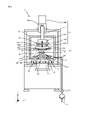
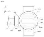
- FIG. 1 is a schematic configuration diagram of a joining system according to Embodiment 1 of the present invention
- FIG. 1 is a schematic front view of a joining apparatus according to Embodiment 1
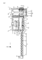
- FIG. 2 is a schematic configuration diagram of a second conveying device, a joining device, and a load lock unit according to Embodiment 1
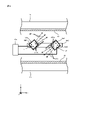
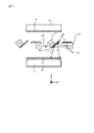
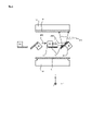
- FIG. 1 is a diagram showing a part of a joining device according to Embodiment 1
- FIG. 4A and 4B are operation explanatory diagrams of the joining apparatus according to Embodiment 1
- FIG. 4A and 4B are operation explanatory diagrams of the joining apparatus according to Embodiment 1
- FIG. 10 is a diagram showing a state in which the holding portion of the second conveying device according to Embodiment 1 is arranged inside the joining device;
- FIG. 8 is a diagram showing a state in which the holding section of the second conveying device according to Embodiment 1 is arranged in the load lock section;
- 4 is a flow chart showing the flow of a joining method according to Embodiment 1.
- FIG. FIG. 3 is a diagram showing a second transport device, a bonding device, and a load lock unit according to Embodiment 1, and showing how the second transport device receives substrates from the load lock unit;
- FIG. 2 shows a second transport device, a bonding device, and a load lock unit according to Embodiment 1, and illustrates how the second transport device transports substrates to the bonding device
- FIG. 4 is a diagram showing a second transport device, a bonding device, and a load lock unit according to Embodiment 1, and showing a state in which substrates are transported to the bonding device
- FIG. 4 is a diagram showing a second transport device, a bonding device, and a load lock unit according to Embodiment 1, and showing how a substrate is held by a head in the bonding device;
- FIG. 3 is a diagram showing a second transport device, a bonding device, and a load lock unit according to Embodiment 1, and showing how the second transport device receives substrates from the load lock unit;
- FIG. 4 is a diagram showing a second transport device, a bonding device, and a load lock unit according to Embodiment 1, and showing how the bonding device receives a substrate from the second transport device;
- FIG. 4 is a diagram showing a second transport device, a bonding device, and a load lock unit according to Embodiment 1, and showing how a substrate is held on a stage in the bonding device;
- FIG. 4 is a diagram showing a second conveying device, a joining device, and a load lock unit according to Embodiment 1, and showing a state in which joining processing is performed in the joining device;
- FIG. 4 is a diagram showing a second transporting device, a bonding device, and a load lock unit according to Embodiment 1, and showing how the second transporting device receives substrates from the bonding device;
- FIG. 2 shows a second transport device, a bonding device, and a load lock unit according to Embodiment 1, and illustrates how the second transport device transports substrates from the bonding device to the load lock unit; It is a figure for demonstrating the measuring method of the bonding strength (surface energy conversion) of a board
- FIG. 4 is a diagram showing the relationship between the bonding strength between substrates and the atmospheric pressure in the chamber during bonding in Embodiment 1.
- FIG. 6 is a flow chart showing the flow of a hydrophilic bonding method according to Embodiment 2 of the present invention.
- 4 is a photograph of two substrates bonded by a hydrophilization bonding method without performing a heat treatment process before an activation treatment process according to a comparative example.
- 4 is a photograph of two substrates bonded by a hydrophilic bonding method according to Embodiment 2.
- FIG. FIG. 11 is a schematic configuration diagram of a joining system according to a modified example;
- FIG. 11 is a schematic configuration diagram of an activation processing device according to a modification; It is a flowchart which shows the flow of the hydrophilization joining method which concerns on a modification. It is a figure which shows a part of joining apparatus which concerns on a modification. It is a figure which shows a part of joining apparatus which concerns on a modification. It is a figure which shows a part of joining apparatus which concerns on a modification. It is a figure which shows a part of joining apparatus which concerns on a modification. It is a figure which shows a part of joining apparatus which concerns on a modification. It is a figure which shows a part of joining apparatus which concerns on a modification.
- the bonding apparatus heats the bonding surfaces of two substrates in a chamber in a reduced-pressure atmosphere, performs an activation process, and then brings the substrates into contact with each other to apply pressure and heat. , to join the two substrates.
- the substrates W1 and W2 include, for example, a Si substrate, a glass substrate such as a SiO2 glass substrate, an oxide substrate (eg, a silicon oxide ( SiO2 ) substrate, an alumina substrate ( Al2O3 ) including a sapphire substrate).
- nitride substrates e.g., silicon nitride (SiN), aluminum nitride (AlN), gallium nitride (GaN)), GaAs substrates, silicon carbide (SiC) substrates, lithium tantalate It is an object to be bonded made of any one of a (Lt:LiTaO 3 ) substrate, a lithium niobate substrate (Ln:LiNbO 3 ), a diamond substrate, and the like.
- the substrates W1 and W2 may be substrates having electrodes formed of a metal such as Au, Cu, Al, or Ti on the bonding surfaces. In the activation process, the bonding surfaces of the two substrates to be bonded to each other are irradiated with a particle beam to activate the bonding surfaces of the substrates.
- the joining system includes introduction ports 811 and 812, an extraction port 813, a first conveying device 82, a cleaning device 3, a joining device 1, a load lock section 83, and a , a second conveying device 84 , and a control unit 9 .
- the control section 9 controls the first conveying device 82 , the cleaning device 3 , the bonding device 1 and the load lock section 83 .
- a HEPA (High Efficiency Particulate Air) filter (not shown) is provided in the first conveying device 82 and the cleaning device 3 .
- the interiors of the first conveying device 82 and the cleaning device 3 are in an atmospheric pressure environment with extremely few particles.
- the first transport device 82 includes a transport robot 821 having an arm provided with a holding portion 821a for holding a substrate at its tip.
- the transfer robot 821 can move along the direction in which the introduction ports 811 and 812 and the extraction port 813 are arranged, and can change the orientation of the tip of the arm by turning.
- the holding part 821a has a vacuum chuck, an electrostatic chuck, or the like, and attracts and holds the side of the substrate opposite to the bonding surface side.
- the cleaning device 3 cleans the transported substrate while ejecting water, a cleaning liquid, or N2 gas.
- the cleaning apparatus 3 includes a stage (not shown) that supports a substrate, a rotary drive unit (not shown) that rotates the stage in a plane perpendicular to the vertical direction, water to which ultrasonic waves or megasonic vibrations are applied, and a cleaning nozzle (not shown) for ejecting cleaning liquid or N2 gas. Then, the cleaning apparatus 3 rotates the substrates W1 and W2 by rotating the stage while spraying water to which ultrasonic waves are applied from the cleaning nozzles onto the bonding surfaces of the substrates while rocking the cleaning nozzles in the radial direction of the substrates W1 and W2. Clean the entire joint surface. Then, the cleaning device 3 spin-dries the substrates W1 and W2 by rotating the stage in a state in which water ejection from the cleaning nozzles is stopped.
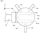
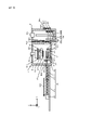
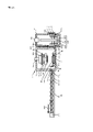
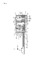
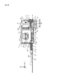
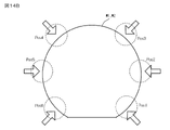
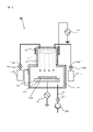
- the bonding apparatus 1 includes a chamber 120, a stage 141, a head 142, a stage driving section 143, a head driving section 144, substrate heating sections 1411 and 1421, and a positional deviation measuring section 150. , and particle beam sources 161 , 162 .
- the ⁇ Z directions in FIG. 2 are appropriately defined as vertical directions, and the XY directions are defined as horizontal directions.
- the bonding apparatus 1 also includes covers 122A and 122B arranged in the chamber 120, and cover heating units 123A and 123B that heat the covers 122A and 122B.
- the covers 122A and 122B are arranged so as to include activation processing areas in the activation processing process around the stage 141 and the head 142, respectively.
- the cover heating units 123A and 123B are heaters fixed to the sides of the covers 122A and 122B opposite to the particle beam sources 161 and 162, respectively.
- the bonding apparatus 1 includes a support mechanism 146 arranged near the stage 141 and receiving the substrates W1 and W2 transferred from the load lock section 83 into the chamber 120, as shown in FIG.
- the chamber 120 is connected to a vacuum pump 121a through an exhaust pipe 121b and an exhaust valve 121c.
- the exhaust valve 121c When the exhaust valve 121c is opened and the vacuum pump 121a is operated, the gas inside the chamber 120 is exhausted to the outside of the chamber 120 through the exhaust pipe 121b, and the pressure inside the chamber 120 is reduced (depressurized).
- the pressure inside the chamber 120 can be set to 10 ⁇ 5 Pa or less.
- the air pressure (degree of vacuum) in the chamber 120 can be adjusted by adjusting the exhaust amount by varying the amount of opening and closing of the exhaust valve 121c.
- the stage 141 and the head 142 are arranged inside the chamber 120 so as to face each other in the Z direction.
- the stage 141 supports the substrate W1 on its upper surface
- the head 142 supports the substrate W2 on its lower surface.
- the upper surface of the stage 141 and the lower surface of the head 142 are roughened in consideration of the case where the contact surfaces of the substrates W1 and W2 with the stage 141 and the head 142 are mirror surfaces and the substrates W1 and W2 are not easily separated from the stage 141 and the head 142.
- the stage 141 and head 142 each have a holding mechanism (not shown) that holds the substrates W1 and W2.
- the holding mechanism has an electrostatic chuck, a mechanical clamp, or the like.
- the stage 141 has a shape in which a stepped portion 141a is formed on the periphery. Then, in a state where the substrates W1 and W2 are placed on the stage 141, the peripheral portions of the substrates W1 and W2 are arranged above the stepped portion 141a.
- the stage drive unit 143 can move the stage 141 in the XY directions and rotate it around the Z axis.
- the head drive unit 144 includes an elevation drive unit 1441 that moves the head 142 up and down as indicated by an arrow AR1, an XY direction drive unit 1442 that moves the head 142 in the XY directions, and a rotation direction around the Z axis that rotates the head 142. and a rotation drive unit 1443 .
- the head driving section 144 also has a piezo actuator 1444 for adjusting the tilt of the head 142 with respect to the stage 141 and a pressure sensor 1445 for measuring the pressure applied to the head 142 .
- the XY-direction drive unit 1442 and the rotation drive unit 1443 move the head 142 relative to the stage 141 in the X direction, the Y direction, and the rotation direction around the Z axis, thereby rotating the substrate W1 held on the stage 141. and the substrate W2 held by the head 142 can be aligned.
- the stage driving section 143 is not limited to the configuration arranged vertically below the stage 141.
- a backup section (not shown) that receives pressure is provided vertically below the stage 141, and the stage driving section 143 may be arranged on the outer periphery of the stage 141 and the stage 141 may be driven from the side of the stage 141 .
- the elevation driving unit 1441 brings the head 142 closer to the stage 141 by moving the head 142 vertically downward.
- the elevation drive unit 1441 moves the head 142 away from the stage 141 by moving the head 142 vertically upward.
- the elevation driving unit 1441 applies a driving force to the head 142 in a direction toward the stage 141 in a state where the substrates W1 and W2 are in contact with each other, the substrate W2 is pressed against the substrate W1.
- the elevation driving section 1441 is provided with a pressure sensor 1441 a that measures the driving force acting on the head 142 in the direction of approaching the stage 141 .
- the pressure sensor 1441a has, for example, a piezoelectric element.
- a plurality of sets of piezo actuators 1444 and pressure sensors 1445 are arranged between the head 142 and the XY direction driving section 1442 .
- the pressure sensor 1445 is interposed between the upper end portion of the piezo actuator 1444 and the lower side of the XY direction driving portion 1442 .
- the piezo actuators 1444 are vertically extendable and retractable, and by extension and retraction, the inclination of the head 142 around the X-axis and the Y-axis and the vertical position of the head 142 are finely adjusted.
- the pressure sensor 1445 has, for example, a piezoelectric element, and measures pressure applied at a plurality of locations on the lower surface of the head 142 .
- the substrates W1 and W2 are moved while maintaining the lower surface of the head 142 and the upper surface of the stage 141 in parallel. can be brought into contact with each other.
- the substrate heating units 1411 and 1421 are electric heaters embedded on the back side of the holding mechanism when viewed from the side of the substrates W1 and W2 in contact with the substrates W1 and W2 in the stage 141 and the head 142. and a first object-to-be-bonded heating unit.
- the substrate heating units 1411 and 1421 heat the substrates W1 and W2 by transferring heat to the substrates W1 and W2 supported by the stage 141 and the head 142 . Further, by adjusting the amount of heat generated by the substrate heating units 1411 and 1421, the temperature of the substrates W1 and W2 or their bonding surfaces can be adjusted.
- the positional displacement amount measuring unit 150 measures the horizontal positional displacement amount of the substrate W1 with respect to the substrate W2 by recognizing the positions of alignment marks (alignment marks) provided on the substrates W1 and W2.
- the positional deviation amount measuring unit 150 recognizes the alignment marks of the substrates W1 and W2, for example, using light (for example, infrared light) that passes through the substrates W1 and W2.
- the stage drive unit 143 moves and rotates the stage 141 in the horizontal direction based on the positional deviation amount measured by the positional deviation amount measuring unit 150, thereby performing alignment operation between the substrates W1 and W2. (alignment operation) is executed. Both the measurement of the positional deviation amount by the positional deviation amount measuring section 150 and the alignment operation of the stage driving section 143 are executed under the control of the control section 9 .
- Each of the particle beam sources 161 and 162 is, for example, a Fast Atom Beam (FAB) source, and for example, as shown in FIG. It is an activation processing section having a beam source drive section 1603 and a gas supply section 1604 for supplying argon gas into the discharge chamber 1601 .
- a peripheral wall of the discharge chamber 1601 is provided with an FAB emission port 1601a for emitting neutral atoms.
- the discharge chamber 1601 is made of a carbon material.
- the discharge chamber 1601 has a long box shape, and a plurality of FAB radiation ports 1601a are arranged in a straight line along its longitudinal direction.
- the beam source driver 1603 includes a plasma generator (not shown) that generates argon gas plasma in the discharge chamber 1601 and a DC power supply (not shown) that applies a DC voltage between the electrode 1602 and the peripheral wall of the discharge chamber 1601 . not shown).
- the beam source driver 1603 applies a DC voltage between the peripheral wall of the discharge chamber 1601 and the electrode 1602 while generating argon gas plasma in the discharge chamber 1601 . At this time, argon ions in the plasma are attracted to the peripheral wall of the discharge chamber 1601 .
- the argon ions heading toward the FAB emission port 1601a receive electrons from the peripheral wall of the discharge chamber 1601 formed of a carbon material on the outer periphery of the FAB emission port 1601a when passing through the FAB emission port 1601a.
- the argon ions are discharged out of the discharge chamber 1601 as electrically neutralized argon atoms.
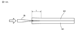
- the particle beam sources 161 and 162 move as indicated by an arrow AR22 while irradiating the bonding surfaces of the substrates W1 and W2 with the particle beams as indicated by an arrow AR21.
- the particle beam sources 161 and 162 have variations in intensity in the moving direction of the particle beam alone in the projection plane.
- the particle beam is irradiated up to a region including the outer cover portions 122A and 122B on both edges of the substrate W1 in the direction of movement of the substrates 161 and 162 .
- the intensity of the particle beam tends to decrease at both ends in the longitudinal direction of the discharge chamber 1601 of the particle beam source 161, that is, in the X-axis direction.
- the length of the discharge chamber 1601 in the X-axis direction is, for example, as shown in FIG.
- the length is set longer than the length of the cover and the substrates W1 and W2 in the X-axis direction.
- the irradiation regions of the particle beam sources 161 and 162 are rectangular in plan view, so regions other than the substrates W1 and W2 are irradiated.
- the bonding apparatus 1 irradiates the bonded surfaces of the substrates W1 and W2 with the particle beam while moving the particle beam sources 161 and 162 in the +Y direction as indicated by an arrow AR22, and then moves the particle beam sources 161 and 162.
- the bonding surfaces of the substrates W1 and W2 are irradiated with a particle beam.
- the moving speeds of the particle beam sources 161 and 162 are set to 1.2 to 14.0 mm/sec, for example.
- the power supplied to the particle beam sources 161 and 162 is set to 1 kV and 100 mA, for example.
- the flow rate of argon gas introduced into the discharge chamber 1601 of each of the particle beam sources 161 and 162 is set at 50 sccm, for example.
- the covers 122A and 122B are made of metal, for example, and arranged around the stage 141 and the head 142 in the chamber 120, respectively.
- the cover heating unit 123A has, for example, an electric heater, and is arranged close to the cover 122A on the -Z direction side of the cover 122A. This cover 122A is fixed to the stage 141 and moves together with the stage 141 .
- the cover heating unit 123B also has, for example, an electric heater, and is arranged close to the cover 122B on the +Z direction side of the cover 122B. This cover 122B is fixed to the head 142 and moves together with the head 142 .
- the support mechanism 146 has a support member 1461 that supports the substrates W1 and W2, and a support member driving section 1462 that moves the support member 1461 up and down.
- the support member 1462 has a substantially L-shaped shape, and the tip extends to a stepped portion 141 a formed on the periphery of the stage 141 .
- three support mechanisms 146 are provided, and in this case, the support members 1461 support three positions on the periphery of the substrates W1 and W2, as shown in FIG. 7A, for example.
- a projection 1461a is provided at the tip of the support member 1462 to support the substrates W1 and W2 at the tip. Then, as shown in FIG.
- the support mechanism 146 drives the support member 1462 in the +Z direction while the tip of the support member 1462 is in contact with the peripheral portions of the substrates W1 and W2 placed on the stage 141. By doing so, the substrates W1 and W2 are lifted.
- This support mechanism 146 is fixed to the stage 141 and moves together with the stage 141 .
- the load lock unit 83 includes a standby chamber 831, an exhaust pipe 832b communicating with the standby chamber 831, a vacuum pump 832a for discharging the gas in the standby chamber 831 through the exhaust pipe 832b, and an exhaust pipe inserted in the exhaust pipe 832b. and a valve 832c.
- the exhaust valve 832c is opened and the vacuum pump 832a is operated, the gas in the chamber 831 is exhausted to the outside of the chamber 831 through the exhaust pipe 832b, and the pressure in the chamber 831 is reduced (depressurized). Note that the pressure inside the chamber 831 can be set to 10 ⁇ 2 Pa or less.
- the load lock unit 83 includes a gate 833a arranged on the side of the first transfer device 82 in the waiting chamber 831, a gate 833b arranged on the side of the bonding device 1 in the waiting chamber 831, and gates 833a and 833b. and a gate driver 834 that drives to open and close separately.
- the load lock unit 83 also includes a substrate holding mechanism 836 that holds the substrates W1 and W2 transported into the standby chamber 831, and a substrate heating unit 835 that heats the substrates W1 and W2.
- the gates 833a and 833b are provided to cover the opening 831a penetrating the waiting chamber 831 on the side of the first transfer device 82 and the opening 831b penetrating on the side of the bonding device 1, respectively.
- the substrate holding mechanism 836 includes a cassette 8361 that holds substrates W1 and W2, a substrate heating unit 8363 that heats the substrates W1 and W2 held at the bottom of the cassette 8361, and lifts and lowers the cassette 8361 as indicated by an arrow AR4. and a lifting drive unit 8362 .
- the cassette 8361 has a plurality (three in FIG. 3) of slots SLT1, SLT2 and SLT3.
- the uppermost slot SLT3 and the lowermost slot SLT1 hold the substrates W1 and W2 before bonding, respectively, and the second uppermost slot SLT2, that is, the central slot SLT2, holds the substrates W1 and W2 after the bonding process. Bonded substrates W1 and W2 are held. Thereby, the heat treatment process by the substrate heating units 835 and 8363 of the substrates W1 and W2 in the load lock unit 83 becomes possible. Further, since the cassette 8361 can hold the substrates W1 and W2 that have been bonded together after the bonding process in the slot SLT2, the substrates W1 and W2 that have been bonded to each other after the bonding process in the bonding apparatus 1 can be stored in the cassette.
- the substrates W1 and W2 held in the slots SLT1 and SLT3 can be transported from the standby chamber 831 to the bonding apparatus 1, and the bonding process can be performed in the bonding apparatus 1.
- FIG. 8 As a result, while the bonding process is being performed in the bonding apparatus 1, the standby chamber 831 is opened to the atmosphere, the mutually bonded substrates W1 and W2 are taken out, and new substrates W1 and W2 are introduced into the standby chamber 831. Since the substrates can be transported, there is no need to release the substrates to the atmosphere multiple times in one cycle, and the substrates can be exchanged one time during bonding efficiently, the processing time can be shortened.
- the substrate heating units 835 and 8363 are second bonding object heating units having lamp heaters, for example.
- the substrate heating section 8363 may have an electric heater, for example.
- the cassette 8361 has support pieces 8361a that support the peripheral portions of the substrates W1 and W2 from both sides of the substrates W1 and W2 in the direction orthogonal to the insertion direction of the substrates W1 and W2, as shown in FIG. 7B, for example.
- a projection 8361b is provided at the tip of the support piece 8361a to support the substrates W1 and W2 at the tip.
- the second transfer device 84 is elongated and is inserted through the opening 120a provided in the chamber 120 of the bonding apparatus 1.
- One end of the second transfer device 84 is provided with a holding portion 845 for holding the substrates W1 and W2. It has a rod 841 , a support 842 that supports the support rod 841 at the other end of the support rod 841 , and a support driver 843 that drives the support 842 .
- the second transfer device 84 also has a bellows 844 interposed between the outer periphery of the opening 120 a of the chamber 120 and the support 842 to maintain the degree of vacuum in the chamber 120 .
- the support drive unit 843 includes, for example, a rail (not shown) that supports a slider (not shown) to which the support 842 is fixed so as to be slidable in the X-axis direction, and a rail for driving the slide in the X-axis direction. a ball screw mechanism (not shown);
- the support drive unit 843 drives the support 842 in the direction in which the support rod 841 is inserted into and removed from the chamber 120 as indicated by an arrow AR3, thereby moving the substrates W1 and W2 between the load lock unit 83 and the bonding apparatus 1. from one to the other.
- the holding portion 845 has a main portion 8452 and two long support pieces 8451 extending in the same direction from the main portion 8452, as shown in FIGS.
- Projections 8453 that support the substrates W1 and W2 at the tip portions are arranged at the central portion in the width direction of the main portion 8452 and the tip portions of the two support pieces 8451, respectively.
- the holding portion 845 has a size and shape that allows it to be inserted between the two support mechanisms 146 of the joining device 1 and between the pair of support pieces 8361 a of the cassette 8361 of the load lock portion 83 .
- control unit 9 is, for example, a programmable logic controller.
- the control unit 9 calculates the pressure when the substrates W1 and W2 are brought into pressure contact with each other based on the measurement signals input from the pressure sensor 148, the positional displacement amount measurement unit 150, and the like, and calculates the relative pressure between the substrates W1 and W2. For example, the amount of positional deviation is calculated.
- control unit 9 outputs control signals to the stage driving unit 143, the head driving unit 144, and the support mechanism 146 based on the calculated pressure or positional displacement amount. Controls the operation of mechanism 146 .
- control unit 9 outputs control signals to the substrate heating units 1411 and 1421, the particle beam sources 161 and 162, the second transport device 84, and the first transport device 82 to control these operations.
- FIG. 8 it is assumed that the substrates W1 and W2 are placed in the introduction ports 811 and 812 shown in FIG.
- a substrate W2 held by the head 142 of the bonding apparatus 1 is placed in the introduction port 811, and a substrate W1 placed on the stage 141 of the bonding apparatus 1 is placed in the introduction port 812, for example.
- a chamber heating step of heating the inner wall of the chamber 120 in advance is performed before performing the bonding method according to the present embodiment.
- a heater jacket (not shown) is wrapped around the peripheral wall of the chamber 120 to heat (bake) the inner wall of the chamber 120 at 150° C. for about 24 hours.
- the pressure inside the chamber 120 can be reduced to 10 ⁇ 5 Pa or less.
- a cover heating process for heating the covers 122A and 122B may be performed at the same time.
- the length of the baking time for baking the chamber 120 in the chamber heating process may be equal to or longer than the length of the cover heating time for heating the covers 122A and 122B in the cover heating process. It may be less than the length.
- water or impurities adhering to the covers 122A and 122B can be removed.
- the first transfer device 82 takes out the substrate W2 placed in the introduction ports 811 and 812 and transfers it to the cleaning device 3 (step S101). ).
- the transport robot 821 rotates while holding the substrates W1 and W2 so that the tip of the arm 821a faces the cleaning apparatus 3 side.
- the transfer robot 821 extends the arm 821a and inserts the tip of the arm 821a into the cleaning apparatus 3.
- the substrates W1 and W2 are transferred from the tip of the arm 821a of the transfer robot 821 to the stage of the cleaning device 3. As shown in FIG.
- the cleaning device 3 performs a water cleaning process for cleaning the substrates W1 and W2 with water (step S102).
- the cleaning device 3 rotates the stage on which the substrates W1 and W2 are placed while spraying water to which ultrasonic waves are applied from the cleaning nozzles onto the bonding surfaces of the substrates W1 and W2, thereby bonding the substrates W1 and W2 together. Clean the entire surface. As a result, foreign matter attached to the joint surfaces of the substrates W1 and W2 is removed.
- the cleaning apparatus 3 stops water discharge from the cleaning nozzles, and then rotates the stage to spin dry the substrate, thereby completing the water cleaning process. After that, the cleaning apparatus 3 opens the loading/unloading port for the substrates W1 and W2 when the series of cleaning processes is completed.
- the first transport device 82 transports the substrates W1 and W2 for which the water cleaning process has been completed from the cleaning device 3 to the load lock section 83 (step S103).
- the transfer robot 821 of the first transfer device 82 extends the arm 821a and inserts the tip of the arm 821a into the cleaning device 3 while the loading/unloading port of the substrates W1 and W2 of the cleaning device 3 is open.
- the substrates W1 and W2 are received from the stage in the cleaning apparatus 3.
- the transport robot 821 takes out the substrates W1 and W2 from the cleaning device 3 by contracting the arm 821a.
- the transfer robot 821 moves the tip of the arm 821a while holding the substrates W1 and W2. turn so that the portion faces the load lock portion 83 side.
- the transfer robot 821 receives the substrate W2 from the cleaning apparatus 3
- the transfer robot 821 reverses the arm 821a so that the bonding surface of the substrate W2 faces vertically downward, so that the bonding surface of the substrate W2 faces vertically downward. It turns while holding the substrate W2 in a facing posture.
- the transfer robot 821 receives the substrate W1 from the cleaning apparatus 3, it turns while maintaining the posture of the substrate W2 with its bonding surface facing vertically upward. After that, the transfer robot 821 inserts the tip of the arm 821a into the waiting chamber 831 by extending the arm 821a. Then, the substrates W1 and W2 are transferred from the tip of the arm 821a to the cassette 8361 of the substrate holding mechanism 836 arranged in the standby chamber 831. FIG. At this time, the substrates W1 and W2 are held in the uppermost slot SLT3 and the lowermost slot SLT1 of the cassette 8361, for example, as shown in FIG. 9A.
- the transport robot 821 retracts the arm 821a. Then, the gate driver 834 closes the gate 833a of the standby chamber 831 .
- a heat treatment process is performed to heat the bonding surfaces of the two substrates W1 and W2 to a temperature higher than 60° C. (step S104).
- the reduced-pressure atmosphere is, for example, a state in which the pressure inside the chamber 120 is 10 ⁇ 2 Pa or less.
- the substrate heating section 835 of the load lock section 83 heats the substrate W2, and the substrate heating section 8363 heats the substrate W1.
- the substrates W1 and W2 are heated by the substrate heating unit 835 arranged above the standby chamber 831 and the substrate heating unit 8363 arranged below.
- the second transport device 84 transports the substrates W1 and W2 held in the cassette 8361 of the substrate holding mechanism 836 from the load lock section 83 to the bonding apparatus 1 (step S105).
- the load lock unit 83 first reduces the pressure in the standby chamber 831 to approximately the same degree of vacuum as the chamber 120 of the bonding apparatus 1 .
- the gate driver 834 opens the gate 833b of the standby chamber 83 on the side of the bonding apparatus 1 .
- the up-and-down driving section 8362 of the load lock section 83 enables the insertion of the holding section 845 of the second transfer device 84 into the lower side of the slot SLT3 holding the substrate W2 of the cassette 8361 as shown in FIG. 9A.
- the second transport device 84 moves the support rod 841 toward the load lock portion 83 as indicated by an arrow AR31, thereby inserting the holding portion 845 into the slot SLT3 holding the substrate W2 in the cassette 8361 below the slot SLT3.
- the lift driving portion 8362 of the load lock portion 83 moves the cassette 8361 vertically downward as indicated by an arrow AR41, thereby transferring the substrate W2 from the cassette 8361 to the holding portion 845.
- the substrate W2 is held by the holding portion 845 with the bonding surface facing vertically downward. are held by point contact, there is no effect on the bonding of the substrates W1 and W2.
- the second transfer device 84 moves the support rod 841 away from the load lock portion 83 as indicated by an arrow AR32 in FIG. do.
- the gate driver 834 closes the gate 833b.
- the support member driving section 1462 of the support mechanism 146 raises the support member 1461 to lift the substrate W2.
- the second transport device 84 moves the support rod 841 away from the load lock portion 83, thereby moving the holding portion 845 to the preset standby position. Deploy.
- the head drive unit 144 of the bonding apparatus 1 moves the head 142 vertically downward as indicated by the arrow AR11 in FIG. After that, the substrate W2 is held by the head 142.
- the load lock unit 83 moves the cassette 8361 to a position where the holding unit 845 of the second transfer device 84 can be inserted under the slot SLT1 holding the substrate W1, as indicated by the arrow AR42.
- the head driving section 144 raises the head 142 as indicated by an arrow AR12 in FIG. 11A.
- the support member driving section 1462 lowers the support member 1461 as indicated by an arrow AR52.
- the gate driver 834 opens the gate 833b of the standby chamber 83 on the side of the bonding apparatus 1 again.
- the second transport device 84 moves the support rod 841 toward the load lock portion 83 as indicated by an arrow AR34, thereby inserting the holding portion 845 into the slot SLT1 holding the substrate W1 in the cassette 8361 below the slot SLT1.
- the lift drive section 8362 of the load lock section 83 moves the cassette 8361 vertically downward as indicated by an arrow AR43, thereby transferring the substrate W1 from the cassette 8361 to the holding section 845.
- the second transfer device 84 moves the support rod 841 away from the load lock portion 83 as indicated by arrow AR35 in FIG. do.
- the gate driver 834 closes the gate 833b.
- the support member driving section 1462 of the support mechanism 146 lifts the substrate W1 by raising the support member 1461 as indicated by an arrow AR53.
- the second transport device 84 moves the support rods 841 away from the load lock unit 83 as indicated by the arrow AR36 in FIG.
- the unit 845 is arranged at a preset standby position.
- the support member driving unit 1462 of the support mechanism 146 lowers the support member 1461 as indicated by the arrow AR54, thereby placing the substrate W1 on the stage 141, and then the stage 141 holds the substrate W1. state.
- a heat treatment process is performed in which the joint surfaces of the two substrates W1 and W2 are heated to a temperature higher than 60° C. in a reduced pressure atmosphere (step S106).
- the reduced-pressure atmosphere is, for example, a state in which the pressure inside the chamber 120 is 10 ⁇ 6 Pa or less.
- Substrate heating units 1411 and 1421 heat substrates W1 and W2 to a temperature higher than 60° C. by transferring heat to substrates W1 and W2 supported by stage 141 and head 142, respectively. As a result, the foreign substances mainly composed of water adhering to the bonding surfaces of the substrates W1 and W2 are removed.
- an activation process is performed to activate the bonding surfaces of the two substrates W1 and W2 under a reduced pressure atmosphere (step S107).
- the bonding apparatus 1 irradiates the bonding surfaces of the substrates W1 and W2 with particle beams emitted from the particle beam sources 161 and 162 as indicated by an arrow AR21 in FIG. Activate the surface.
- a cooling process for cooling the substrates W1 and W2 to a temperature of 60° C. or less may be performed.
- a bonding step of bonding the substrates W1 and W2 together is performed (step S108).
- the head drive unit 144 of the bonding apparatus 1 first brings the head 142 supporting the substrate W2 closer to the stage 141 supporting the substrate W1 to bring the two substrates W1 and W2 closer together. Subsequently, the head drive unit 144 performs an alignment operation of the substrates W1 and W2 based on the positional displacement amount measured by the positional displacement amount measuring unit 150 while the substrates W1 and W2 are close to each other. In this way, the head drive unit 144 performs the alignment operation after the activation process, thereby reducing the positional deviation of the substrates W1 and W2.
- the head driving unit 144 brings the two substrates W1 and W2 into contact by bringing the head 142 closer to the stage 141 again, as indicated by the arrow AR12 in FIG. 12B.
- the head driving unit 144 joins the two substrates W1 and W2 by applying pressure in a direction in which the two substrates W1 and W2 are brought into close contact with each other while the joining surfaces of the substrates W1 and W2 are in contact with each other. do.
- the head drive unit 144 raises the head 142 as indicated by an arrow AR13 in FIG. 13A.
- the support member driving section 1462 of the support mechanism 146 raises the substrates W1 and W2 bonded to each other by raising the support member 1461 as indicated by an arrow AR55.
- the load lock unit 83 allows the insertion of the holding unit 845 of the second conveying device 84 into the second stage from the top of the cassette 8361, that is, the upper side of the central slot SLT2, as indicated by an arrow AR44. move it to the desired position.
- the second transport device 84 transports the bonded substrates W1 and W2 from the bonding device 1 to the load lock unit 83 (step S109).
- the second transfer device 84 moves the support rod 841 from the standby position in a direction approaching the load lock portion 83 as indicated by an arrow AR37 in FIG. It is arranged below the substrates W1 and W2.
- the gate drive section 834 of the load lock section 83 opens the gate 833b of the standby chamber 831 on the bonding apparatus 1 side.
- the support member driving section 1462 of the support mechanism 146 lowers the support member 1461 as indicated by the arrow AR56 in FIG.
- the second transport device 84 moves the support rod 841 from the standby position toward the load lock portion 83 as indicated by an arrow AR38, thereby moving the holding portion 845 above the center slot SLT2 of the cassette 8361. insert into Then, the lift driving portion 8362 of the load lock portion 83 lifts the cassette 8361 by a preset distance as indicated by an arrow AR45, thereby transferring the substrates W1 and W2 from the holding portion 845 to the cassette 8361. . After that, the second transport device 84 moves the support rod 841 to the standby position. Gate driver 834 then closes gate 833b.
- the first transfer device 84 then transfers the bonded substrates W1 and W2 from the load lock section 83 to the removal port 813 (step S110).
- the load lock unit 83 opens the standby chamber 831 to the atmosphere.
- the gate drive section 834 of the load lock section 83 opens the gate 833a on the side of the first transfer device 82 in the standby chamber 831, and the transfer robot 821 directs the tip of the arm 821a toward the load lock section 83 side. In this state, the arm 821 a is extended and the tip of the arm 821 a is inserted into the standby chamber 831 .
- the substrates W1 and W2 bonded to each other are transferred from the stage in the standby chamber 831 to the tip of the arm 821a of the transfer robot 821.
- the gate driving section 834 of the load lock section 83 closes the gate 833a.
- the transfer robot 821 turns so that the tip of the arm 821a faces the take-out port 813 side.
- the transport robot 821 extends the arm 821a while holding the bonded substrates W1 and W2, inserts the tip of the arm 821a into the extraction port 813, and removes the bonded substrates W1 and W2. Placed in extraction port 813 .
- the chamber 120 Before performing the above-described bonding method, the chamber 120 is decompressed and the chamber 120 is heated, that is, after the chamber 120 is baked, the covers 122A and 122B are heated by the cover heating units 123A and 123B.
- a cover heating step of heating may be performed.
- the cover heating step of heating the cover while the pressure inside the chamber 120 is reduced may be performed.
- the results of evaluating the bonding strength of ten types of samples obtained by bonding two substrates W1 and W2 by the bonding system according to the present embodiment will be described.
- the amount of argon gas supplied to each of the particle beam sources 161 and 162 in the activation process was set to 50 sccm.
- the degree of vacuum in the chamber 120 was set to 2 ⁇ 10 ⁇ 6 Pa immediately before the particle beam sources 161 and 162 irradiated the substrates W1 and W2 with the particle beams.
- a pressure of 20000 N was applied in a direction in which the two substrates W1 and W2 were in close contact with each other, and the pressure was maintained for 60 seconds.
- Si substrates were used as the substrates W1 and W2.
- the stage (head) temperature before the substrates W1 and W2 are held by the stage 141 and the head 142 and the stage (head) temperature from the load lock unit 83 to the stage of the bonding apparatus 1
- a summary of the stage temperature immediately after being transported to 141, the pre-contact temperature in the separated state before the substrates W1 and W2 are brought into contact with each other, and the post-contact temperature after the substrates W1 and W2 are brought into contact. are shown in Table 1 below.
- samples 1 to 7 after the substrates W1 and W2 are transported from the load lock unit 83 to the stage 141 and the head 142 of the bonding apparatus 1, the standing time until the bonding process including the activation process is performed.
- stage 141 and head 142 were heated to 300° C. before substrates W1 and W2 were held by stage 141 and head 142, and then cooled to 25° C. and 150° C., respectively. After that, the substrates W1 and W2 were transported from the load lock section 83 to the bonding apparatus 1. As shown in FIG. Furthermore, for sample 7, the substrates W1 and W2 in contact with each other were heated to 150° C. after the activation process and the contacting step were completed. After the sample 3 was transported from the load lock unit 83 to the bonding apparatus 1, the temperatures of the stage 141 and the head 142 were raised to 150° C. with the substrates facing each other separated, and then the activation process was performed. , the substrates W1 and W2 were brought into contact with each other and bonded.
- the standing time after the substrates W1 and W2 are transported from the load lock unit 83 to the bonding apparatus 1 until the bonding process is performed is summarized. It is shown in Table 2 below.
- Table 2 the temperature of the stage 141 and the head 142 before the substrates W1 and W2 were set on the stage 141 and the head 142 was set to 80.degree.
- the temperature immediately after being transported from the load lock unit 83 to the bonding apparatus 1 and the temperature during bonding of the substrates W1 and W2 were set to 80° C. as in the case of the sample 6, respectively.
- Table 3 summarizes the presence or absence of heat treatment after transporting the substrates W1 and W2 into the standby chamber 831 for each of the samples 9 and 10 out of the ten types of samples.
- “with heat treatment” indicates that the substrate heating section 835 in the load lock section 83 performed heating at 100° C. for 10 minutes.
- the standing time from transporting from the load lock unit 83 to the bonding apparatus 1 to performing the bonding process was set to 30 seconds.
- stage (head) temperature before the substrates W1 and W2 are held by the stage 141 and the head 142 of the bonding apparatus 1, the temperature immediately after being transported from the load lock unit 83 to the bonding apparatus 1, and the temperature before the contact Both the temperature and the post-contact temperature were set to normal temperature, that is, 25°C.
- the bonding strengths of the substrates W1 and W2 of Samples 1 to 10 were evaluated by measuring the bonding strength (converted to surface energy) using a crack-and-opening method in which a blade is inserted.
- W2 are measured.
- the blade BL is inserted into six locations (Pos1, Pos2, Pos3, Pos4, Pos5, Pos6) on the peripheral edge of the two substrates W1 and W2 that are bonded to each other (see arrows in FIG. 14B). ) was measured.
- the strength of the bonding interface between the substrates W1 and W2 is calculated in terms of the surface energy per unit area from the separation length L for each of the six peripheral portions of the substrates W1 and W2.
- a strength evaluation was performed.
- the bonding strength (in terms of surface energy) Eb from the peel length L the following relational expression (1) was used.
- Y indicates Young's modulus
- Ts indicates the thickness of the substrates W1 and W2
- Tb indicates the thickness of the blade BL.
- the Young's modulus Y was set to 6.5 ⁇ 10 10 [N/m 2 ], and the thickness Ts of the substrates W1 and W2 was set to 0.0011 m (1. 1 mm), and the thickness Tb of the blade BL was 0.0001 m (0.1 mm).
- Table 5 shows the average peel length and bonding strength (in terms of surface energy) at 6 locations on the peripheral edges of the substrates W1 and W2, and the number of measurement points at which bulk fracture occurred. The larger the calculated bonding strength (converted to surface energy), the greater the bonding strength between the substrates W1 and W2. Bulk failure in excess of 2 J/m 2 is generally preferred.
- the peeling length is also shown.
- Table 4 shows the evaluation results of the bonding strength of the substrates W1 and W2 for the samples 1 to 10.
- Column of “Sample Name” in Table 4 corresponds to Samples 1 to 14 in Table 1 described above.
- the values in the "Peeling Length” column indicate the average values of the peeling lengths at six locations ("Pos1" to “Pos6") on the peripheral edges of the two substrates W1 and W2 shown in FIG. 14B.
- the values in the column of "bonding strength (converted to surface energy)” are bonding strengths (converted to surface energy) at six locations ("Pos1" to “Pos6" on the peripheral edge portions of the two substrates W1 and W2 shown in FIG. 14B.
- the bonding strength (in terms of surface energy) of Samples 2 and 3 was both 2.5 J/m 2 or more, and all six points reached the bulk breaking strength, whereas the sample Bonding strengths (converted to surface energy) of 1 and 7 were both less than 2.5 J/m 2 .
- the temperatures of the substrates W1 and W2 before being held by the stage 141 and the head 142 are maintained at room temperature, that is, about 25° C., bonding from the load lock portion 83 It was found that the bonding strength between the substrates W1 and W2 is greatly increased by raising the temperature immediately after being conveyed to the apparatus 1 and the temperature before contact to 150°C.
- the bonding strength (converted to surface energy) of sample 4 was less than 2.5 J/m 2
- the bonding strength (converted to surface energy) of samples 3, 5, and 6 were all 2.5 J. /m 2 or more.
- all six locations reached the bulk breaking strength. From these results, the substrates W1 and W2 were heated to a temperature higher than 60.degree. It was found that the bonding strength between the substrates W1 and W2 increased, and in particular, the bonding strength between the substrates W1 and W2 increased significantly by raising the temperature immediately before bonding the substrates W1 and W2 to 100° C. or higher.
- the bulk breaking strength of sample 6 was reached at two locations, while the bulk breaking strength of sample 8 was reached at four locations. From this result, when the temperatures of the substrates W1 and W2 before being held by the stage 141 and the head 142, that is, when the temperature immediately before bonding the substrates W1 and W2 is 80° C., the substrates W1 and W2 are at the load lock portion. It has been found that the bond strength between the substrates W1 and W2 is improved by extending the standing time until the bonding process is performed after the substrates W1 and W2 are transported from 83 to the bonding apparatus 1 .
- the bond strength (converted to surface energy) of sample 10 is less than 2.5 J/m 2
- the bond strength (converted to surface energy) of sample 9 is 2.5 J/m 2 or more
- Bulk breaking strength was reached at two locations. From this, it has been found that heating the substrates W1 and W2 in the load lock section 83 also contributes to the improvement in bonding strength between the substrates W1 and W2. It was also found that the air pressure in the heat treatment process should be 10 ⁇ 2 Pa or less. Note that the bonding strength of sample 9 is lower than that of sample 5 . From this, it was found that the atmospheric pressure in the heat treatment step is more preferably 10 ⁇ 5 Pa or less.
- the principle of direct bonding by this activation treatment is that impurities on the surface are removed by the Ar particle beam, and dangling bonds that serve as binding hands are exposed by removing molecular bonds, and other impurities and impurities are removed.
- the dangling bonds of the other substrate can be directly bonded at room temperature in an environment where the molecules are not floating. Therefore, in a vacuum where impurities float, dangling bonds are terminated by the impurities, making bonding impossible.
- the bond strength (converted to surface energy) of the substrates W1 and W2 exhibits a dependency as shown in FIG. 15, for example, on the pressure inside the chamber 120 in the activation process.
- the results shown in FIG. 15 are obtained when both substrates W1 and W2 are Si substrates. From the results shown in FIG. 15, the pressure inside the chamber 120 in the activation treatment process rapidly increases from 10 ⁇ 5 Pa or less.
- a heater jacket (not shown) is wrapped around the peripheral wall of the chamber 120 and the inside of the chamber 120 is heat-treated (baked) at 150° C. for about 24 hours. This is achieved by removing impurities, mainly moisture in the chamber 120 . The reason why the results shown in FIG.
- the substrates W1 and W2 themselves are also subjected to heat treatment in the same manner to remove impurities mainly composed of moisture, so that the bonding strength between the substrates W1 and W2 is further improved. I can understand the reasoning.
- Si substrates were used as the substrates W1 and W2.
- Alumina substrates including sapphire substrates (Al 2 O 3 ), gallium oxide (Ga 2 O 3 ), etc.), nitride substrates (e.g., silicon nitride (SiN), aluminum nitride (AlN), gallium nitride (GaN)), GaAs
- SiC silicon carbide
- LiTaO3 lithium tantalate
- LiNbO3 lithium niobate
- the case where the substrates W1 and W2 made of materials having different coefficients of linear expansion are bonded together was also evaluated.
- a Si substrate was used as the substrate W1
- a lithium tantalate (Lt:LiTaO 3 ) substrate or a lithium niobate substrate (Ln:LiNbO 3 ) was used as the substrate W2, and the bonding method described above was performed.
- the bonding strength between the substrates W1 and W2 (in terms of surface energy) is ) was 1.0 J/m 2 .
- the substrates W1 and W2 are cooled to 60° C. and then bonded together. increased to 1.6 J/m 2 . That is, the bonding strength between the substrates W1 and W2 was improved when the substrates W1 and W2 were bonded after the temperature of the substrates W1 and W2 decreased to a temperature lower than the temperature during the heat treatment after the heat treatment. This is because when the substrates W1 and W2 are bonded to each other while the substrates W1 and W2 are maintained at a relatively high temperature during the heat treatment, the substrates W1 and W2 have different linear expansion coefficients.
- the cleaning device 3 water cleaning is performed in the cleaning device 3, and water attached to the bonding surfaces of the substrates W1 and W2 is removed by a spin dry method. , W2.
- the bonding strength (in terms of surface energy) between the substrates W1 and W2 was 0.5 J/m 2 or less.
- the substrates W1 and W2 are washed with water in the washing device 3, and after removing the water adhering to the bonding surfaces of the substrates W1 and W2 by a spin dry method, the wafers are carried into the load lock unit 83, and the substrates W1 and W2 are transferred to the load lock unit 83 or the bonding apparatus 1.
- the bonding strength (converted to surface energy) between the substrates W1 and W2 was greater than 2.5 J/m 2 . That is, the bonding strength between the substrates W1 and W2 could be improved even if the water cleaning was performed before the bonding process. This is because water is removed by the spin dry method after washing with water in the washing apparatus 3, but when the heat treatment process of the substrates W1 and W2 is not performed, water molecules remain as a thin layer on the bonding surfaces of the substrates W1 and W2. It is thought that this is the reason why the bonding strength between the substrates W1 and W2 is lower than the bonding strength between the substrates W1 and W2 when the water cleaning is not performed.
- the bonding strength between the substrates W1 and W2 was improved because substantially all of the water remaining on the bonding surfaces of the substrates W1 and W2 was removed by performing the heat treatment process for the substrates W1 and W2. Further, it can be seen from this result that when water remains on the bonding surfaces of the substrates W1 and W2, the water remaining on the substrates W1 and W2 cannot be completely eliminated simply by leaving the substrates W1 and W in a vacuum atmosphere. This result shows that water remains on the bonding surfaces of the substrates W1 and W2 even in a vacuum atmosphere, and that heating the substrates W1 and W2 in a vacuum atmosphere is effective in completely removing the water.
- the time-dependent change in bonding strength when Si substrates are used as the substrates W1 and W2 and the bonding surfaces of the substrates W1 and W2 are irradiated with a particle beam and then the substrates W1 and W2 are bonded to each other are examined for the heat treatment described above. A comparison was made between the case where the process was performed and the case where the heat treatment process was not performed. The number of times of particle beam irradiation was reduced in order to reduce the bond strength between the substrates W1 and W2 to some extent and to facilitate checking of changes in the bond strength between the substrates W1 and W2 over time. As a result, the bonding strength between the substrates W1 and W2 when the heat treatment process was performed was more than double that when the heat treatment process was not performed.
- the bonding surfaces of the two substrates W1 and W2 are heated to 60° C. under a reduced pressure atmosphere while the two substrates W1 and W2 are separated from each other. After performing a heat treatment step of heating to a temperature higher than that, an activation treatment step of activating the bonding surfaces of the substrates W1 and W2 is performed. After that, the bonding apparatus 1 bonds the two substrates W1 and W2 under a reduced pressure atmosphere. As a result, water or impurities existing on the bonding surfaces of the substrates W1 and W2 are vaporized and removed by heating the bonding surfaces of the two substrates W1 and W2 to a temperature higher than 60° C.
- the bonding surfaces of the substrates W1 and W2 are easily activated by the activation process. Therefore, it is possible to increase the bonding strength between the two substrates W1 and W2 when bonding the two substrates W1 and W2 after the activation process.
- the DC voltage applied between the electrode 1602 of the particle beam sources 161 and 162 and the peripheral wall of the discharge chamber 1601 is 1 kV
- the current flowing between the electrode 1602 and the peripheral wall of the discharge chamber 1601 is 100 mA
- the flow rate of the Ar gas introduced into 1601 is set to 50 sccm
- the particle beam continues to irradiate the bonding surfaces of the substrates W1 and W2.
- the bonding surfaces of the substrates W1 and W2 may be irradiated with the particle beam more than necessary. As a result, the bonding strength between the substrates W1 and W2 is lowered.
- the bonding surfaces of the two substrates W1 and W2 are heated to a temperature higher than 60° C. before the activation process. Any impurities present are removed.
- the bonded surfaces of the substrates W1 and W2 are formed to a thickness of about 1 nm, that is, a thickness corresponding to one atomic layer exposed at the bonded surfaces of the substrates W1 and W2. It is possible to expose the dangling bonds necessary for enhancing the bonding between the substrates W1 and W2 while maintaining the flatness of the bonding surfaces of the substrates W1 and W2. Therefore, the bonding strength between the substrates W1 and W2 can be increased.
- the substrates W1 and W2 are introduced from the atmosphere, moisture and impurities adhere to the bonding surfaces of the substrates W1 and W2. Therefore, it is considered that impurities containing water molecules as a main component adhere to the surfaces of the substrates W1 and W2.
- the substrates W1 and W2 are heated before the activation process. can be effectively removed.
- water since water is crystallized under a reduced pressure atmosphere, it can be vaporized (sublimated) and easily removed by heating the substrates W1 and W2.
- the impurities are considered to be mainly water, since they are removed at around 100°C. In other words, it is preferable to remove the impurities mainly composed of water molecules by heating in a reduced pressure atmosphere rather than by etching such as particle beam irradiation, which may roughen the bonding surfaces of the substrates W1 and W2.
- the bonding system according to the present embodiment after cleaning in the cleaning device 3 , the workpiece is put into the bonding device 1 . A large amount of water molecules adhere to the bonding surfaces of the substrates W1 and W2 during cleaning by the cleaning device 3, but can be removed by performing a heat treatment process in the bonding device 1. FIG. Therefore, a cleaning process for removing particles from the bonding surfaces of the substrates W1 and W2 with water can be performed before the bonding process, which is preferable from the viewpoint of suppressing voids that occur in the bonded substrates W1 and W2. .
- the particle beams emitted from the particle beam sources 161 and 162 are emitted from the particle beam sources 161 and 162 in order to ensure that the entire substrate W1 is irradiated with the particle beams.
- a region including portions of the covers 122A, 122B outside the edges of the substrates W1, W2 in the direction is irradiated.
- the particle beam sources 161 and 162 tend to have greatly reduced particle beam intensities at both ends in the longitudinal direction of the elongated discharge chamber 1601 . Therefore, the lengths of the particle beam sources 161 and 162 are set longer than the longitudinal lengths of the particle beam sources 161 and 162 on the substrates W1 and W2, as shown in FIG.
- the particle beams emitted from the particle beam sources 161 and 162 are irradiated onto regions including the outer cover portions 122A and 122B on both edges of the substrates W1 and W2 in the longitudinal direction of the particle beam sources 161 and 162, respectively. Therefore, if impurities adhere to the surfaces of the covers 122A and 122B, the impurities adhered to the surfaces of the covers 122A and 122B are repelled by the particle beams irradiated to the covers 122A and 122B during the activation process, and the substrates are exposed to the substrate. There is a possibility that it will adhere to the joint surfaces of W1 and W2.
- the covers 122A and 122B are heated before performing the activation process, thereby removing impurities attached to the surfaces of the covers 122A and 122B.
- impurities it is possible to prevent impurities from adhering to the bonding surfaces of the substrates W1 and W2 due to the impurities adhering to the surfaces of the covers 122A and 122B being repelled by the particle beam during the activation process.
- the heat treatment process is performed immediately before the activation treatment process.
- the impurities mainly composed of water are removed to some extent in advance in the load lock section 83, the impurities mainly composed of water are further removed in the heat treatment process in the bonding apparatus 1.
- the time required for the heat treatment process in the apparatus 1 can be shortened. Therefore, the time required for the entire processing performed on the substrates W1 and W2 in the bonding apparatus 1 can be shortened, and the processing efficiency can be improved accordingly.
- the bonding strength between the substrates W1 and W2 is lowered as compared with the case where the heat treatment process is performed in the bonding apparatus 1. . Therefore, it is preferable to perform the heat treatment process in the bonding apparatus 1 after performing the heat treatment process in the load lock section 83 .
- the bonding surfaces of the substrates W1 and W2 are contaminated with impurities mainly composed of water.
- the heat treatment process is primarily performed in the load lock section 83 in a reduced pressure atmosphere of 10-2 Pa, and then the heat treatment process is further performed in the bonding apparatus 1 in a reduced pressure atmosphere of 10-5 Pa.
- impurities adhering to the bonding surfaces of the substrates W1 and W2 can be substantially completely removed, so that bonding strength between the substrates W1 and W2 can be improved.
- Sample 8 was subjected to heat treatment for 10 minutes in the load lock portion 83, one cycle of the bonding system according to this embodiment is approximately 15 minutes.
- the heat treatment for 10 minutes in the load lock section 83 can be performed without reducing the cycle time of one cycle.
- the bonding strength between the substrates W1 and W2 made of SiN was measured. was evaluated in air, in N 2 atmosphere and in vacuum (1 ⁇ 10 ⁇ 3 Pa) using the aforementioned crack and opening method.
- the N 2 atmosphere contains less water than the air, and a vacuum of 1 ⁇ 10 ⁇ 3 Pa was used in order to further reduce the amount of water in the environment.
- the bonding strength was 1.1 J/m 2 in the atmosphere, it was 1.5 J/m 2 in the N 2 atmosphere and 2.5 J/m 2 or more in vacuum.
- the bonding system according to the present embodiment differs from that of the first embodiment in that the substrates W1 and W2 are bonded together by so-called hydrophilization.
- the bonding system according to the present embodiment performs an activation treatment process for activating the bonding surfaces of the substrates W1 and W2, and then performs a water washing process for washing the bonding surfaces of the substrates W1 and W2 with water.
- the configuration of the joining system according to this embodiment is the same as the joining system described in the first embodiment. In the following, configurations similar to those of the first embodiment will be described using the same reference numerals as those shown in FIGS. 1 to 3.
- FIG. The pressure inside the chamber 120 of the bonding apparatus 1 can be set within a range of 1 Pa or more and 1000 Pa or less.
- the bonding system according to the present embodiment performs so-called hydrophilization bonding between the substrates W1 and W2
- the substrates W1 and W2 are placed in the introduction ports 811 and 812 shown in FIG.
- a substrate W2 held by the head 142 of the bonding apparatus 1 is placed in the introduction port 811, and a substrate W1 placed on the stage 141 of the bonding apparatus 1 is placed in the introduction port 812, for example.
- the first transport device 82 takes out the substrates W2 placed in the introduction ports 811 and 812 and transports them to the load lock section 83 (step S201).
- the transport robot 821 takes out the substrates W1 and W2 from the introduction ports 811 and 812 . Then, when the gate drive unit 834 of the load lock unit 83 opens the gate 833a of the standby chamber 831 on the side of the first transfer device 82, the transfer robot 821 moves the tip of the arm 821a while holding the substrates W1 and W2. turns to face the load lock portion 83 side. At this time, when the substrate W2 is taken out from the introduction port 812, the transfer robot 821 reverses the arm 821a so that the bonding surface side of the substrate W2 faces vertically downward, so that the bonding surface of the substrate W2 faces vertically downward. It turns while holding the substrate W2 in a facing posture.
- the transport robot 821 rotates while maintaining the attitude of the substrate W2 so that the bonding surface faces vertically upward. After that, the transfer robot 821 inserts the tip of the arm 821a into the waiting chamber 831 by extending the arm 821a. Then, the substrates W1 and W2 are transferred from the tip of the arm 821a to the cassette 8361 of the substrate holding mechanism 836 arranged in the standby chamber 831. FIG. Next, when the transfer of the substrates W1 and W2 to the cassette 8361 of the substrate holding mechanism 836 is completed, the transport robot 821 retracts the arm 821a. Then, the gate driver 834 closes the gate 833a of the standby chamber 831 .
- step S202 transports the substrates W1 and W2 held in the cassette 8361 of the substrate holding mechanism 836 from the load lock section 83 to the bonding apparatus 1 (step S202). Note that the operation in step S202 is the same as the operation in step S105 described in the embodiment.
- step S203 an activation process is performed to activate the bonding surfaces of the two substrates W1 and W2 in a reduced pressure atmosphere. Note that the operation in step S203 is the same as the operation in step S107 described in the embodiment.
- the second transport device 84 transports the substrates W1 and W2 from the bonding device 1 to the load lock section 83 (step S204).
- the second transfer device 84 for example, transfers the substrates W1 and W2 to the lowermost slot SLT1 and the uppermost slot SLT3 of the cassette 8361, respectively.
- the transport robot 821 transports the substrates W1 and W2 to the cleaning device 3 (step S205).
- the gate drive section 834 of the load lock section 83 opens the gate 833a of the waiting chamber 831 on the side of the first transfer device 82
- the transfer robot 821 takes out the substrates W1 and W2 from the cassette 8361 in the waiting chamber 831.
- the transfer robot 821 turns so that the tip of the arm 821a faces the cleaning apparatus 3 side while holding the substrates W1 and W2.
- the transport robot 821 extends the arm 821 a and inserts the tip of the arm 821 a into the cleaning device 3 .
- the substrates W1 and W2 are transferred from the tip of the arm 821a of the transfer robot 821 to the stage of the cleaning device 3. As shown in FIG.
- the cleaning device 3 performs a water cleaning process for cleaning the substrates W1 and W2 with water (step S206).
- This water washing process corresponds to a hydrophilization treatment process for hydrophilizing the bonding surfaces of the substrates W1 and W2.
- the cleaning device 3 corresponds to a hydrophilization device that uses water to hydrophilize.
- the first transport device 82 transports the substrates W1 and W2 for which the water cleaning process has been completed from the cleaning device 3 to the load lock unit 83 (step S207).
- a heat treatment process is performed to heat the joint surfaces of the two substrates W1 and W2 to a temperature higher than 60° C. (step S208).
- the second transport device 84 transports the substrates W1 and W2 held in the cassette 8361 of the substrate holding mechanism 836 from the load lock section 83 to the bonding apparatus 1 (step S209).
- a heat treatment process is performed in which the bonding surfaces of the two substrates W1 and W2 to be bonded to each other are heated to a temperature higher than 60° C. in a reduced pressure atmosphere (step S210).
- the inside of the chamber 120 is maintained under a reduced pressure within a range of 10000 Pa or less in order to reduce voids involving air. Only water molecules are removed, and many OH groups that contribute to bonding between the substrates W1 and W2 exist on the bonding surfaces of the substrates W1 and W2.
- the degree of vacuum in the chamber 120 is preferably 1000 Pa or less, more preferably 1 Pa or less, and more preferably 10 ⁇ 2 Pa or less.
- the pressure in the chamber 120 can be reduced to 10000 Pa or less by providing the load lock unit 83 and introducing a gas such as nitrogen containing no moisture into the chamber 120 of the bonding apparatus 1. is preferred.
- the operations in steps S207 to S210 are respectively the same as the operations in steps S103 to S106 described in the embodiment. Thereafter, a bonding process is performed to bond the substrates W1 and W2 together (step S211).
- the second transport device 84 transports the bonded substrates W1 and W2 from the bonding device 1 to the load lock unit 83 (step S212). Subsequently, the first transport device 84 transports the bonded substrates W1 and W2 from the load lock section 83 to the take-out port 813 (step S213).
- the operations in steps S212 and S213 are the same as the operations in steps S109 and S110 described in the embodiment.
- the pressure in the chamber 120 is set to 1000 Pa or less to bond the substrates W1 and W2 together. do.
- excess water that causes microvoids adhering to the bonding surfaces of the substrates W1 and W2 due to the heat treatment process performed before the substrates W1 and W2 are brought into contact with each other in the chamber 120 can be removed.
- the OH groups formed on the bonding surfaces of the substrates W1 and W2 come into direct contact with each other, so that after bonding the substrates W1 and W2 together, the OH groups adhere to the bonding surfaces of the substrates W1 and W2. It is possible to reduce the processing temperature and shorten the processing time in the step of performing the annealing treatment for removing excess water. For example, the processing temperature in annealing can be reduced from 350.degree. C. to 150.degree. Therefore, it is possible to bond the substrates W1 and W2 together at a relatively low temperature in a short period of time.
- an activation treatment step is performed to generate a sufficient amount of OH groups on the bonded surfaces of the substrates W1 and W2, thereby interposing the substrates W1 and W2 together.
- Water and impurities can be substantially eliminated, and since the OH groups formed on the bonding surfaces of the substrates W1 and W2 are directly bonded to each other, an increase in bonding strength between the substrates W1 and W2 can be expected.
- the appearance and bonding strength (surface energy conversion) will be described.
- the bonding strength (in terms of surface energy) between the substrates W1 and W2 was 1.9 mJ/m 2 .
- the activation process was performed after the heat treatment process as in the hydrophilic bonding method according to the present embodiment, no microvoids were observed as shown in FIG. 17B.
- the bonding strength (in terms of surface energy) between the substrates W1 and W2 was also greater than 2.5 mJ/m 2 .
- the bonding method according to the present embodiment was also evaluated in the case where the substrates W1 and W2 made of materials having different coefficients of linear expansion were bonded together.
- a Si substrate is used as the substrate W1
- a lithium tantalate (Lt:LiTaO 3 ) substrate or a lithium niobate substrate (Ln:LiNbO 3 ) is used as the substrate W2. gone.
- the substrates W1 and W2 are subjected to a heat treatment process to remove moisture adhering to the bonding surfaces of the substrates W1 and W2 so that excess moisture does not remain on the bonding interfaces of the substrates W1 and W2. preferably.
- a heat treatment process to remove moisture adhering to the bonding surfaces of the substrates W1 and W2 so that excess moisture does not remain on the bonding interfaces of the substrates W1 and W2. preferably.
- hydrophilization bonding and good results were obtained by removing excess moisture by heat treatment before bonding.
- at least one of the joint surfaces of the two objects to be joined is heated to a temperature higher than 60° C. in a reduced pressure atmosphere. It suffices to bond two objects to be bonded.
- the substrates W1 and W2 are bonded together in the atmosphere, air or excess water is caught between the bonded surfaces of the substrates W1 and W2, which causes voids.
- the hydrophilization bonding method according to the present embodiment the substrates W1 and W2 are bonded together in a reduced pressure atmosphere with little air or moisture, so the occurrence of voids as described above is suppressed.
- the bonding surfaces of the two substrates W1 and W2 to be bonded to each other are heated to a temperature higher than 60° C. in a reduced-pressure atmosphere. A heat treatment process is performed.
- the substrates W1 and W2 are bonded together using a bonding system that includes the load lock section 83 . Therefore, it is not necessary to open the chamber 120 of the bonding apparatus 1 to the atmosphere, so that the processing time can be shortened accordingly.
- the joining system includes introduction ports 811 and 812, an extraction port 813, a first conveying device 82, a cleaning device 3, a joining device 1, a load lock section 83, and a second 2 transport device 84, activation processing device 2002, and control unit 9 may be provided.
- the same reference numerals as in FIG. 1 denote the same configurations as in the embodiment.
- the activation processing apparatus 2002 performs activation processing for activating the bonding surfaces of the substrates W1 and W2 by performing at least one of reactive ion etching using nitrogen gas and nitrogen radical irradiation. conduct. An activation process is performed to activate the bonding surface of the substrate.
- the activation processing device 2002 is a device for generating inductively coupled plasma (ICP), and as shown in FIG. It has a wound induction coil 215 and a high frequency power supply 216 that supplies a high frequency current to the induction coil 215 .
- the activation processing apparatus 2 may be of a type in which, for example, plasma is generated in the upper part of the chamber and only radicals contained in the plasma are caused to flow down through holes formed in the ion trap plate.
- the plasma generation source may be a parallel plate type plasma generation source or a plasma generation source using microwaves.
- the plasma chamber 213 is made of quartz glass, for example.
- the activation processing device 2002 also has a nitrogen gas supply section 220A and an oxygen gas supply section 220B.
- the nitrogen gas supply section 220A has a nitrogen gas reservoir 221A, a supply valve 222A, and a supply pipe 223A.
- the oxygen gas supply section 220B has an oxygen gas reservoir 221B, a supply valve 222B, and a supply pipe 223B.
- Substrates W1 and W2 are placed on the stage 210 . Further, the stage 210 is provided with a substrate heating section 210a for heating the substrates W1 and W2. Chamber 212 communicates with plasma chamber 213 .
- the chamber 212 is connected to a vacuum pump 201a via an exhaust pipe 201b and an exhaust valve 201c.
- the exhaust valve 201c is opened and the vacuum pump 201a is operated, the gas in the chamber 212 is exhausted to the outside of the chamber 212 through the exhaust pipe 201b, and the pressure in the chamber 212 is reduced (depressurized).
- the pressure inside the chamber 212 can be set to 10 ⁇ 2 Pa or less.
- the high-frequency power supply 216 one that supplies a high-frequency current of, for example, 27 MHz to the induction coil 215 can be adopted.
- a high-frequency current is supplied to the induction coil 215 while the N 2 gas is introduced into the plasma chamber 213 , plasma PLM is formed within the plasma chamber 213 .
- the bias application unit 217 is a high frequency power supply that applies a high frequency bias to the substrates W1 and W2 supported by the stage 210.
- the bias applying section 217 for example, one that generates a high frequency bias of 13.56 MHz can be employed.
- a high-frequency bias to the substrates W1 and W2 from the bias applying unit 217 in this manner, a sheath region is generated in the vicinity of the bonding surfaces of the substrates W1 and W2 where ions having kinetic energy repeatedly collide with the substrates W1 and W2. do.
- the bonding surfaces of the substrates W1 and W2 are etched by ions having kinetic energy present in the sheath region.
- the first transfer device 82 takes out the substrates W2 arranged in the introduction ports 811 and 812 and transfers them to the activation processing device 2002 (step S301).
- the transport robot 821 takes out the substrates W1 and W2 from the introduction ports 811 and 812 .
- the transfer robot 821 turns so that the tip of the arm 821a faces the activation processing device 2002 while holding the substrates W1 and W2.
- the transfer robot 821 rotates while maintaining the substrates W1 and W2 taken out from the introduction ports 811 and 812 in a posture in which the bonding surface faces vertically upward.
- the transfer robot 821 inserts the tip of the arm 821a into the chamber 212 by extending the arm 821a. Then, the substrates W1 and W2 are transferred from the tip of the arm 821a to the stage 210 inside the chamber 212. As shown in FIG. Next, when the transfer of the substrates W1 and W2 to the stage 210 is completed, the transfer robot 821 retracts the arm 821a.
- the substrate heating section 210 a heats the substrates W 1 and W 2 with the substrates W 1 and W 2 placed on the stage 210 .
- an activation process is performed to activate the bonding surfaces of the substrates W1 and W2 in a reduced pressure atmosphere (step S302).
- the reduced-pressure atmosphere is, for example, a state in which the pressure inside the chamber 212 is 1 ⁇ 10 ⁇ 2 Pa or less.
- the activation processing apparatus 2002 introduces N2 gas into the chamber 212 from the nitrogen gas reservoir 221A through the supply pipe 223A by opening the supply valve 222A shown in FIG. 16, for example.
- the activation processing apparatus 2002 applies a high frequency bias to the substrates W1 and W2 placed on the stage 210 by the bias applying section 217 while stopping the supply of the high frequency current from the high frequency power supply 216 to the induction coil 215. apply.
- the bonding surface of the substrate W1 is subjected to reactive ion etching (RIE) using N2 gas.
- RIE reactive ion etching
- the activation processing device 2002 starts supplying high-frequency current from the high-frequency power supply 216 to the induction coil 215 to generate plasma with N2 gas.
- the activation processing apparatus 2002 stops application of the high-frequency bias to the substrate W1 by the bias applying unit 217.
- FIG. In this manner, the bonding surface of the substrate W1 is irradiated with N2 radicals.
- the activation processing apparatus 2002 when activating the bonding surface of the substrate W2, that is, the Si or nitride substrate, the activation processing apparatus 2002 first opens the supply valve 222B, thereby supplying oxygen gas from the oxygen gas reservoir 221B to the chamber 212 through the supply pipe 223B. O2 gas is introduced inside. Next, the activation processing apparatus 2002 applies a high frequency bias to the substrate W2 placed on the stage 210 by the bias applying section 217 while stopping the supply of the high frequency current from the high frequency power supply 216 to the induction coil 215. . As a result, the bonding surface of the substrate W2 is subjected to reactive ion etching (RIE) using O2 gas.
- RIE reactive ion etching
- the activation processing apparatus 2002 closes the supply valve 622B to stop the supply of O2 gas from the O2 gas reservoir 621B into the chamber 612, thereby exhausting the O2 gas in the chamber 612.
- the activation processing apparatus 2002 introduces N2 gas into the chamber 212 from the nitrogen gas reservoir 221A through the supply pipe 223A by opening the supply valve 222A.
- the activation processing device 2002 starts supplying high-frequency current from the high-frequency power supply 216 to the induction coil 215 to generate plasma with N2 gas.
- the activation processing apparatus 2002 stops application of the high-frequency bias to the substrate W2 by the bias applying section 217.
- the bonding surface of the substrate W2 is irradiated with N2 radicals.
- a cover (not shown) is placed in the chamber 212 so as to include the activation process areas around the substrates W1 and W2 to be activated. ) may be performed at the same time.
- the transport robot 821 transports the substrates W1 and W2 to the cleaning device 3 (step S303).
- the transfer robot 821 takes out the substrates W1 and W2 placed on the stage 210 within the chamber 212 of the activation processing apparatus 2002 .
- the cleaning apparatus 3 opens the loading/unloading port for the substrates W1 and W2
- the transfer robot 821 turns so that the tip of the arm 821a faces the cleaning apparatus 3 side while holding the substrates W1 and W2.
- the transport robot 821 extends the arm 821 a and inserts the tip of the arm 821 a into the cleaning device 3 .
- the substrates W1 and W2 are transferred from the tip of the arm 821a of the transfer robot 821 to the stage of the cleaning device 3. As shown in FIG.
- the cleaning device 3 performs a water cleaning process for cleaning the substrates W1 and W2 with water (step S304).
- the first transport device 82 transports the substrates W1 and W2 for which the water cleaning process has been completed from the cleaning device 3 to the load lock unit 83 (step S305).
- the transfer robot 821 receives the substrate W2 from the cleaning apparatus 3, the transfer robot 821 reverses the arm 821a so that the bonding surface of the substrate W2 faces vertically downward, so that the bonding surface of the substrate W2 faces vertically downward. After turning while holding the substrate W2 in a facing posture, the substrate W2 is transported to the load lock unit 83 .
- a heat treatment process is performed to heat the bonding surfaces of the two substrates W1 and W2 to a temperature higher than 60° C. (step S306).
- the second transport device 84 transports the substrates W1 and W2 held in the cassette 8361 of the substrate holding mechanism 836 from the load lock section 83 to the bonding apparatus 1 (step S307).
- a heat treatment process is performed in which the joint surfaces of the two substrates W1 and W2 are heated to a temperature higher than 60° C. in a reduced pressure atmosphere (step S308).
- a bonding process is performed to bond the substrates W1 and W2 together (step S309).
- the second transport device 84 transports the bonded substrates W1 and W2 from the bonding device 1 to the load lock unit 83 (step S310).
- the first transport device 84 transports the bonded substrates W1 and W2 from the load lock section 83 to the take-out port 813 (step S311).
- the operations in steps S310 and S311 are the same as the operations in steps S109 and S110 described in the embodiment.
- the number of steps can be reduced when the substrates W1 and W2 are so-called hydrophilized and bonded, so the time required for bonding the substrates W1 and W2 can be shortened.
- the head driving unit 144 determines the amount of displacement based on the displacement amount measured by the displacement amount measuring unit 150 while the substrates W1 and W2 are in close proximity to each other.
- the head driving unit 144 may perform the alignment operation of the substrates W1 and W2 before performing the activation processing step.
- the bonding process can be performed immediately after the activation treatment process, the substrates W1 and W2 can be bonded together with their bonding surfaces activated.
- the heat treatment process in step S104 or the heat treatment process in step S106 may be omitted.
- heat treatment in step S106 is performed in a reduced pressure atmosphere of about 10 ⁇ 6 Pa.
- the bonding strength between the substrates W1 and W2 is greatly increased under a reduced pressure atmosphere of 10 ⁇ 6 Pa. Therefore, from the viewpoint of firmly bonding the substrates W1 and W2 together, It is preferable to omit the heat treatment process in step S104 rather than omit the heat treatment process in step S106.
- the load lock portion 83 may be omitted.
- the atmospheric pressure in the chamber 120 of the bonding apparatus 1 may be set within the range of 1 Pa or more and 1000 Pa or less. , W2, the processing time does not become extremely long. Therefore, the load lock portion 83 can be omitted in the modified example of the hydrophilic bonding method described above.
- the bonding surfaces of the substrates W1 and W2 may be chemically processed using a wet treatment to generate OH groups on the bonding surfaces of the substrates W1 and W2, and then the substrates W1 and W2 may be bonded together.
- the substrates W1 and W2 may be bonded together after performing only the water cleaning step without the activation treatment step.
- the method of heat-treating the covers 122A and 122B may be performed simultaneously when the chamber 120 is baked, or when performing the heat-treating process of the substrates W1 and W2 before performing the activation process. You can go at the same time.
- W2 may be irradiated.
- the particle beam sources 161 and 162 may irradiate the bonding surfaces of the substrates W1 and W2 with Si particles together with argon.
- a plasma generation source may be employed instead of the particle beam sources 161 and 162 .
- the heat treatment process may be performed only in the bonding apparatus 1 without performing the heat treatment process in the load lock section 83 .
- a Si particle depositing step of depositing Si particles on the joint surface of at least one of the two substrates W1 and W2 may be performed.
- two particle beam sources 161 and 162 may be used to irradiate the bonding surfaces of the substrates W1 and W2 with Si particles.
- the target material TA made of Si is fixed to the side surface of the particle beam source 161, and the particle beam source 162 is fixed to the particle beam source 161 as indicated by the arrow AR41.
- the target material TA is sputtered by irradiating a particle beam toward the target material TA.
- the target material TA fixed to the particle beam source 161 is sputtered by the particle beam incident from the particle beam source 162, and Si particles are irradiated from the target material TA to the bonding surface of the substrate W1 as indicated by an arrow AR42.
- two particle beam sources 161 and 162 to which the target material TA is fixed correspond to the Si particle irradiation section.
- a Si layer is formed on the bonding surface of the substrate W1. Also, as shown in FIG.
- the target material TA made of Si is fixed to the side surface of the particle beam source 162, and the particle beam source 161 is fixed to the particle beam source 162 as indicated by the arrow AR44.
- the target material TA is sputtered by irradiating a particle beam toward the target material TA.
- the target material TA fixed to the particle beam source 162 is sputtered by the particle beam incident from the particle beam source 161, and Si particles are irradiated from the target material TA to the bonding surface of the substrate W2 as indicated by an arrow AR45. be.
- a Si layer is formed on the bonding surface of the substrate W2.
- the Si layers may be etched by irradiating the Si layers with a particle beam.
- the substrates W1 and W2 are made of SiO2
- bonding the substrates W1 and W2 together after forming a Si layer on the bonding surfaces of the substrates W1 and W2 further improves the bonding strength between the substrates W1 and W2.
- the Si layer by depositing Si particles on the substrates W1 and W2 and etching the Si layer by irradiating a particle beam containing Ar at the same time, the deposition amount of the Si particles and the etching of the Si layer It is difficult to adjust the balance with the amount.
- the sputtering time of the target TA by the particle beam source 161 and the substrate W1 , W2 are irradiated with the particle beam, and the balance between the thickness of the Si layer formed by sputtering and the amount of etching by the particle beam can be appropriately adjusted as described above.
- a Si layer or an island-like region formed from Si can be formed.
- the electrodes are exposed on the substrates W1 and W2, by forming an Si layer or an island-like region formed of Si with an optimum thickness, the electrodes are prevented from being electrically connected to each other.
- the bonding strength between the substrates W1 and W2 can be increased.
- the substrates W1 and W2 are Si substrates
- impurities mainly composed of water floating in the chamber 120 are removed by increasing the degree of vacuum.
- the strength is rapidly improved by being Based on this result, in this modified example, especially when the substrates W1 and W2 are made of a material other than Si, by irradiating the bonding surfaces of the substrates W1 and W2 with Si particles to form a Si layer, It was possible to improve the bonding strength between the substrates W1 and W2 bonded together by the bonding method in which the substrates W1 and W2 are subjected to a heat treatment process.
- the substrates W1 and W2 are formed of SiO 2
- the substrates W1 and W2 are separated from each other depending on whether the Si layer is formed on the bonding surface of the substrates W1 and W2 or when the Si layer does not exist.
- the result of comparing the joint strength when joined will be described.
- four samples 11 to 14 were produced and their bonding strength was evaluated. Note that samples 11 to 14 were manufactured under conditions in which the bonding strength was lower than the conditions described in the embodiment in order to facilitate confirmation of changes in the bonding strength between the substrates W1 and W2 over time. is.
- the sample 11 is obtained by scanning the substrates W1 and W2 multiple times with the two particle beam sources 161 and 162 set in the attitude shown in FIG.
- the particle beam sources 161 and 162 are set in a posture for irradiating the substrates W1 and W2 with the particle beams, and the substrates W1 and W2 are scanned once.
- Sample 12 was subjected to heat treatment at 150° C. for 10 minutes after the same treatment as Sample 11 was performed on the substrates W1 and W2.
- the sample 13 is prepared by scanning the substrates W1 and W2 a plurality of times with the two particle beam sources 161 and 162 set in the attitude shown in FIG. , the particle beam sources 161 and 162 are set in a posture for irradiating the substrates W1 and W2 with the particle beams, and the substrates W1 and W2 are scanned a plurality of times.
- the substrates W1 and W2 were subjected to heat treatment at 150° C. for 10 minutes.
- the Si layers of samples 11 and 12 are thinner than the Si layers of samples 13 and 14 .
- the Si layers of samples 11 and 12 are less than 3 nm, and the Si layers of samples 13 and 14 are 3 nm or more.
- the bonding strengths of the samples 11 and 12 are approximately equal at about 0.5 mJ/m 2 .
- the bonding strength of sample 14 (1.49 mJ/m 2 ) was greater than the bonding strength of sample 13 (1.15 mJ/m 2 ). From this, when the Si layer is relatively thin, the effect of improving the bonding strength between the substrates W1 and W2 by the heat treatment does not last, and when the Si layer becomes thicker to some extent, the effect of improving the bonding strength between the substrates W1 and W2 by the heat treatment. persists.
- the moisture remaining at the bonding interface between the substrates W1 and W2 is reduced, thereby suppressing the stress corrosion of the area susceptible to the moisture existing at the bonding interface, thereby suppressing the stress corrosion of the substrate.
- the principle that the bonding strength between W1 and W2 is improved can be derived from the evaluation results of samples 11 to 14 described above. However, this evaluation result shows an example of the factor of the bonding strength improvement effect by the heat treatment described above, and the bonding strength improvement effect is not limited to this factor.
- the substrates W1 and W2 are sapphire substrates
- the bonding surfaces of the substrates W1 and W2 are irradiated with a particle beam containing carbon and when the bonding surfaces of the substrates W1 and W2 are irradiated with a particle beam containing Si particles
- the substrates W1 and W2 are separated from each other.
- the result of comparing the bonding strength when bonding is described.
- four samples 15 to 18 were produced and their bonding strength was evaluated. Note that samples 15 to 18 were manufactured under conditions in which the bonding strength was lower than the conditions described in the embodiment, in order to facilitate confirmation of changes in the bonding strength between the substrates W1 and W2 over time. is.
- the sample 15 was produced by performing an activation treatment step of irradiating particle beams containing carbon from the particle beam sources 161 and 162 to the substrates W1 and W2.
- the substrates W1 and W2 were subjected to heat treatment at 110° C. for 10 minutes.
- the sample 17 was produced by performing an activation treatment step of irradiating particle beams containing Si particles from the particle beam sources 161 and 162 to the substrates W1 and W2.
- the substrates W1 and W2 were subjected to heat treatment at 110° C. for 10 minutes.
- the bond strengths of samples 17 and 18 decreased to 0.6 to 0.7 mJ/m 2 and became substantially equal. From this, it is considered that when the substrates W1 and W2 are sapphire substrates, the moisture remaining at the bonding interface between the substrates W1 and W2 has little effect on the bonding strength.
- the bonding method including the Si particle deposition step according to this modification is effective when the substrates W1 and W2 are made of SiO2 .
- the method of irradiating the bonding surfaces of the substrates W1 and W2 with Si particles is not limited to the Si particle irradiation method described above.
- the bonding surfaces of the substrates W1 and W2 may be irradiated with Si particles. Forming the Si layer on the bonding surfaces of the substrates W1 and W2 by irradiating the bonding surfaces of the substrates W1 and W2 with the Si particles in this manner is equivalent to separating the substrates W1 and W2 from each other as described in the first embodiment.
- At least one of the substrates W1 and W2 has a bonding surface as indicated by an arrow AR51 in FIG. may be irradiated with Si particles together with the particle beam.
- the Si particles are implanted into the bonding surfaces of the substrates W1 and W2.
- the Si particles implanted into the bonding surfaces of the substrates W1 and W2 are etched by a particle beam containing Ar or N2 , the Si particles do not deposit to form an Si layer, and the bonding surfaces are Si-rich. surface can be modified.
- the bonding surfaces of the substrates W1 and W2 are made of Si
- impurities mainly composed of moisture floating in the chamber 120 increase the degree of vacuum.
- the strength is abruptly improved by being removed by Based on this result, in this modification, especially when the substrates W1 and W2 are made of a material other than Si, by implanting Si particles into the bonding surfaces of the substrates W1 and W2, the substrates W1 and W2 are The bonding strength between the substrates W1 and W2 bonded together by a bonding method that performs a heat treatment process is improved.
- the heat treatment process is preferably performed after Si particles are implanted into the bonding surfaces of the substrates W1 and W2. Further, after the substrates W1 and W2 are subjected to the heat treatment process, the Si particles are added to the substrates W1 and W2 while maintaining the temperature in the vicinity of the processing temperature in the heat treatment process without cooling the substrates W1 and W2 to 60°C. It is preferable to perform the activation process while implanting the bonding surface of W2, and then bring the substrates W1 and W2 into contact with each other at a temperature close to the processing temperature in the heat treatment process.
- the bonding strength between the substrates W1 and W2 was 1.6 mJ/m 2 .
- the bonding strength between the substrates W1 and W2 is 2. It was 5 J/m 2 or more (14.3 J/m 2 ), and there were 4 bulk fracture points. That is, the bonding strength between the substrates W1 and W2 was improved. Incidentally, when the substrates W1 and W2 were not subjected to the heat treatment process, the bonding strength between the substrates W1 and W2 was 1.3 J/m 2 .
- the bonding strength between the substrates W1 and W2 is 1 J/ m2 to 1.3 J/m2. 2 , and furthermore, the bonding strength was improved to 14.3 J/m 2 by subjecting the substrates W1 and W2 to the heat treatment process. That is, the bonding strength between the substrates W1 and W2 was only improved by about 0.3 J/m 2 by simply implanting Si particles into the bonding surfaces of the substrates W1 and W2. It was found that the bonding strength between the substrates W1 and W2 was greatly improved to 13.3 J/m 2 .
- an insulating film made of an oxide film, a nitride film, or the like is ion-crystalline and cannot be bonded by so-called direct bonding in which an activation process using a particle beam is performed.
- the bonding strength between the substrates W1 and W2 could not be obtained only by the above method.
- Si particles are implanted into the bonding surfaces of the substrates W1 and W2, and the substrates W1 and W2 are subjected to a heat treatment process, so that even the insulating films made of an oxide film, a nitride film, or the like are bonded together. I was able to connect.
- oxide films made of lithium tantalate (Lt:LiTaO 3 ), lithium niobate substrate (Ln:LiNbO 3 ), etc. used in SAW filters can be strongly bonded together. performance can be improved.
- so-called hybrid bonding in which a metal electrode made of Cu, Au, etc. and an insulating film made of an oxide film, a nitride film, etc. coexist on substantially the same surface, is used to bond the surfaces to each other, which causes a short circuit between the metal electrodes. I was able to do it without any problems.
- the method of implanting Si particles into the bonding surfaces of the substrates W1 and W2 in the activation treatment process is applicable not only to the so-called direct bonding of the substrates W1 and W2 described in the first embodiment.
- the bonding strength between the substrates W1 and W2 can be improved even when the substrates W1 and W2 having the bonding surfaces implanted with Si particles are used for hydrophilic bonding.
- OH groups are attached to the Si particles implanted into the bonding surfaces of the substrates W1 and W2.
- the amount of OH groups present in increases. This improves the bonding strength between the substrates W1 and W2.
- the bonding system includes, for example, an ion implantation device that implants ions into one of two objects to be bonded, and a first heat treatment device that heats the bonding surfaces of the two objects to be bonded to each other under a reduced pressure atmosphere.
- an activation processing device for activating at least one bonding surface of two objects to be bonded; a bonding device; It may be provided.
- at least one of the two objects to be bonded may be a lithium tantalate (Lt:LiTaO 3 ) substrate or a lithium niobate (Ln:LiNbO 3 ) substrate.
- the two bonded objects may be acoustic wave devices or optical modulators.
- At least one of the two objects to be bonded is previously ion-implanted.
- ions may be implanted into both of the two objects to be bonded.
- an ion implanter is often provided separately from the bonding system described above.
- the bonding apparatus includes, for example, a chamber, a stage arranged in the chamber for supporting one of two objects to be bonded, and a stage facing the stage in the chamber to support one of the two objects to be bonded. and a drive unit for moving at least one of the stage and the head in a first direction in which the stage and the head approach each other or in a second direction in which the stage and the head move away from each other. There may be. Then, the control unit controls the first heat treatment apparatus to heat the bonding surfaces of the two objects to be bonded to each other to a temperature of 60° C. or more and less than 150° C. in a reduced pressure atmosphere, and then activates the bonding surfaces.
- the drive section is controlled to activate at least the stage and the head while maintaining the reduced pressure atmosphere.
- the two objects to be bonded are joined by moving one of them in the first direction, and then the second heat treatment device is controlled to bring the two objects to be joined together to a temperature of 210° C. or more and less than 300° C. It may be heated.
- the first heat treatment apparatus may be one in which at least one of the head and the stage is provided with a heater, or may be one used as the above-described second heat treatment apparatus.
- the two objects to be bonded are subjected to heat treatment in the second heat treatment device.
- a conveying apparatus may be provided for conveying two objects to be bonded that are bonded together.
- the transport device may maintain the two bonded objects to be transported at a temperature of 50° C. or higher when transporting the two bonded objects.
- SAW filters manufactured by bonding a lithium tantalate (Lt:LiTaO 3 ) substrate or a lithium niobate (Ln:LiNbO 3 ) substrate to a Si substrate, a SiO 2 substrate, a sapphire substrate, etc.
- the thickness of the lithium tantalate (Lt:LiTaO 3 ) substrate or the lithium niobate (Ln:LiNbO 3 ) substrate must be reduced to about several ⁇ m in order to improve the frequency characteristics.
- the thickness of the lithium tantalate (Lt:LiTaO 3 ) substrate or the lithium niobate (Ln:LiNbO 3 ) substrate should be at least within 10 ⁇ m.
- an optical modulator using the lithium niobate (Ln:LiNbO 3 ) substrate as an optical waveguide may be fabricated.
- the lithium tantalate (Lt:LiTaO 3 ) substrate can be used as an optical waveguide. It is good also as an optical modulator which carries out.
- smart cut technology has been used as a manufacturing technology for SOI (Silicon on Insulator) substrates.
- SOI Silicon on Insulator
- hydrogen atoms are implanted into a Si single crystal substrate at a high concentration to a depth of several ⁇ m by an ion implantation method, and then the Si single crystal substrate is heat-treated at a temperature of 200° C. or higher.
- This is a microfabrication technology that cuts the bonds between Si atoms and separates the entire surface of the Si single crystal substrate by a thickness of several ⁇ m.
- Application to fabrication of SOI devices, single-crystal Si thin films for next-generation solar cells, etc. is being promoted.
- the bonding method according to this modified example is a method developed to cope with these applications. Then, after performing heat treatment at a temperature of 60° C. or more and less than 150° C., activation treatment is performed, and then bonding is performed. Then, the temperature of the object to be bonded is not lowered to a temperature at which cracking or warping occurs, and heat treatment is performed by heating to a temperature of 200° C. or higher while maintaining the temperature at which cracking or warping does not occur.
- separation can be performed at a depth of about several ⁇ m where the ions are implanted without cracking or warping, so a thin lithium tantalate (Lt:LiTaO3) substrate or lithium niobate (Ln:LiNbO3) substrate can be separated.
- the substrate can be manufactured easily.
- the bonding strength between the lithium tantalate (Lt:LiTaO 3 ) substrate or the lithium niobate (Ln:LiNbO 3 ) substrate and the so-called support substrate such as a Si substrate is increased. This is a new method that could not be achieved with the conventional room temperature bonding, as it can be made higher.
- the temperature in the heat treatment is preferably 60°C or higher and lower than 150°C.
- the difference between the temperature at the time of joining after heat treatment and the temperature at the time of additional heat treatment for smart cut is less than 150 ° C., warping or cracking occurs, so 210 ° C. or more and less than 300 ° C. is preferred.
- Smart cut can be performed by heating to 210° C. when the heat treatment temperature is 60° C., and to 300° C. when the temperature is 150° C.
- a thin lithium tantalate (Lt:LiTaO 3 ) substrate or lithium niobate (Ln:LiNbO 3 ) substrate having a thickness of several ⁇ m is firmly bonded to the supporting substrate.
- the remaining lithium tantalate (Lt:LiTaO 3 ) substrate or lithium niobate (Ln:LiNbO 3 ) substrate separated by smart cut is separated in an additional heat treatment step to separate the bonded substrate and the remaining substrate. and may be discharged separately. Alternatively, it may be peeled off after being discharged from the second heat treatment apparatus.
- the above heat treatment and the additional heat treatment can be performed in the same heat treatment apparatus, but since it takes time to raise or lower the temperature, the two heat treatments are performed in different heat treatment apparatuses from the viewpoint of improving mass productivity. preferably implemented. However, since the temperature of the object to be bonded is lowered when the object to be bonded is transported, it is preferable to heat the object to be bonded during transportation. By maintaining the temperature at 50° C. or higher after the heat treatment described above until the additional heat treatment is performed, it is possible to suppress the occurrence of warping or cracking during the additional heat treatment.
- the objects to be bonded are the substrates W1 and W2
- the objects to be bonded are not limited to this, and for example, the objects to be bonded may be a chip and a substrate.
- Water cleaning may be performed in the treatment method.
- the water cleaning treatment may be performed after the bonding surfaces of the substrates W1 and W2 are treated with hydrofluoric acid, other acid, organic solvent, or the like. That is, the method of water cleaning treatment is not particularly limited as long as particles and other substances adhering to the bonding surfaces of the substrates W1 and W2 are removed by cleaning with water.
- the substrates W1 and W2 were subjected to a heat treatment process, a cooling process, a hydrophilization process, a cleaning process, a process of implanting Si into the bonding surface, and a Si particle deposition process of depositing Si particles on the bonding surface.
- the method is not necessarily limited to performing all of these series of steps on both substrates W1 and W2.
- only one of the substrates W1 and W2 may be subjected to the entire series of steps described above.
- cover heating units 123A and 123B are heaters fixed to the sides of the covers 122A and 122B opposite to the particle beam sources 161 and 162, respectively.
- covers 5122A and 5122B are each formed in a plate shape from glass, for example, as shown in FIG.
- the cover heating portions 5123A and 5123B may be heaters composed of conductor patterns embedded in the covers 5122A and 5122B.
- the cover heating portions 5123A and 5123B are composed of conductor patterns laid so as to cover the entire covers 5122A and 5122B.
- a cover heating step of heating the covers 5122A and 5122B is performed at the same time. At this time, since the cover heating portions 5123A and 5123B are embedded in the covers 5122A and 5122B, the covers 5122A and 5122B are heated uniformly and efficiently. to a temperature higher than the temperature of chamber 120 .
- the chamber Water or impurities adhering to 120 may detach from chamber 120 and adhere to covers 122A and 122B.
- the impurities adhering to the covers 122A and 122B are sputtered by the particle beam and float inside the chamber 120 .
- water or impurities floating in the chamber 120 may adhere to the bonding surfaces of the substrates W1 and W2, reducing the bonding strength between the substrates W1 and W2.
- the dummy substrate and the covers 122A and 122B are irradiated with a particle beam to perform so-called blank bombardment.
- a step of removing water or impurities adhering to the covers 122A and 122B is performed.
- this so-called blank firing process takes about 1 to 4 hours, resulting in a loss of processing time.
- the discharge chamber 1601 made of a carbon material is additionally worn by the use of the particle beams 161 and 162 for blank firing.
- a cover heating process is performed in which the entire covers 5122A and 5122B are heated to a temperature higher than the temperature of the chamber 120 by the cover heating units 5123A and 5123B.
- This can suppress adhesion of water or impurities desorbed from the chamber 120 to the covers 5122A and 5122B.
- water or impurities adhering to the bonding surfaces of the substrates W1 and W2 can be removed, similarly to the effect of the heat treatment process described in the embodiment. Therefore, even if the time for performing the above-described so-called blank firing process is shortened or omitted, the bonding strength between the substrates W1 and W2 can be ensured.
- the crack and opening method described above is used to evaluate the bonding strength between the substrates W1 and W2. process may be performed.
- the environment in which the bonding strength is evaluated contains water, stress corrosion of the bonding interface due to the water progresses, and the bonding strength that can be obtained becomes lower than the actual bonding strength.
- the bonding strength between the substrates W1 and W2 can be evaluated with high accuracy.
- the present invention is suitable for manufacturing, for example, CMOS (Complementary MOS) image sensors, memories, arithmetic elements, and MEMS (Micro Electro Mechanical Systems).
- CMOS Complementary MOS
- MEMS Micro Electro Mechanical Systems
Landscapes
- Engineering & Computer Science (AREA)
- Computer Hardware Design (AREA)
- Microelectronics & Electronic Packaging (AREA)
- Power Engineering (AREA)
- Physics & Mathematics (AREA)
- Condensed Matter Physics & Semiconductors (AREA)
- General Physics & Mathematics (AREA)
- Manufacturing & Machinery (AREA)
- Chemical & Material Sciences (AREA)
- Mechanical Engineering (AREA)
- Geochemistry & Mineralogy (AREA)
- Life Sciences & Earth Sciences (AREA)
- Chemical Kinetics & Catalysis (AREA)
- General Chemical & Material Sciences (AREA)
- Materials Engineering (AREA)
- Organic Chemistry (AREA)
- Toxicology (AREA)
- Health & Medical Sciences (AREA)
- Plasma & Fusion (AREA)
- Ceramic Engineering (AREA)
- Robotics (AREA)
- Pressure Welding/Diffusion-Bonding (AREA)
- Container, Conveyance, Adherence, Positioning, Of Wafer (AREA)
Abstract
Ce procédé de jonction permettant de joindre deux substrats (W1, W2) comprend : une étape de traitement thermique consistant à chauffer des surfaces de jonction à joindre l'une à l'autre, de chaque substrats (W1, W2), à une température supérieure à 60° dans une atmosphère à pression réduite ; après l'étape de traitement thermique, une étape de traitement d'activation consistant à activer les surfaces de jonction de chaque substrat (W1, W2) en même temps que l'atmosphère à pression réduite est maintenue ; et, après l'étape de traitement d'activation, une étape de jonction consistant à joindre les deux substrats (W1, W2) en même temps que l'atmosphère à pression réduite est maintenue. En outre, dans l'étape de traitement thermique, un état dans lequel les surfaces de jonction de chaque substrat (W1, W2) ont été chauffées à une température supérieure à 60 °C en même temps que l'atmosphère à pression réduite est maintenue peut être maintenu pendant 30 secondes ou plus. La pression atmosphérique dans l'étape de traitement thermique peut être inférieure ou égale à 10-2 Pa.
Priority Applications (5)
| Application Number | Priority Date | Filing Date | Title |
|---|---|---|---|
| US18/262,187 US20240066624A1 (en) | 2021-01-21 | 2022-01-21 | Bonding method, bonder, and bonding system |
| EP22742682.2A EP4282572A1 (fr) | 2021-01-21 | 2022-01-21 | Procédé de jonction, dispositif de jonction, et système de jonction |
| CN202280011240.4A CN117121158A (zh) | 2021-01-21 | 2022-01-21 | 接合方法、接合装置及接合系统 |
| JP2022576760A JP7460095B2 (ja) | 2021-01-21 | 2022-01-21 | 接合方法、接合装置および接合システム |
| JP2024034755A JP2024056041A (ja) | 2021-01-21 | 2024-03-07 | 接合方法 |
Applications Claiming Priority (6)
| Application Number | Priority Date | Filing Date | Title |
|---|---|---|---|
| JP2021008275 | 2021-01-21 | ||
| JP2021-008275 | 2021-01-21 | ||
| JP2021162509 | 2021-10-01 | ||
| JP2021-162509 | 2021-10-01 | ||
| JPPCT/JP2022/001970 | 2022-01-20 | ||
| PCT/JP2022/001970 WO2022158520A1 (fr) | 2021-01-21 | 2022-01-20 | Procédé de jonction, dispositif de jonction et système de jonction |
Publications (1)
| Publication Number | Publication Date |
|---|---|
| WO2022158563A1 true WO2022158563A1 (fr) | 2022-07-28 |
Family
ID=82548797
Family Applications (1)
| Application Number | Title | Priority Date | Filing Date |
|---|---|---|---|
| PCT/JP2022/002175 WO2022158563A1 (fr) | 2021-01-21 | 2022-01-21 | Procédé de jonction, dispositif de jonction, et système de jonction |
Country Status (5)
| Country | Link |
|---|---|
| US (1) | US20240066624A1 (fr) |
| EP (1) | EP4282572A1 (fr) |
| JP (2) | JP7460095B2 (fr) |
| TW (1) | TW202245178A (fr) |
| WO (1) | WO2022158563A1 (fr) |
Citations (11)
| Publication number | Priority date | Publication date | Assignee | Title |
|---|---|---|---|---|
| JP2004297693A (ja) * | 2003-03-28 | 2004-10-21 | Fujitsu Media Device Kk | 弾性表面波デバイスの製造方法及び弾性表面波デバイス |
| JP2008071787A (ja) * | 2006-09-12 | 2008-03-27 | Ushio Inc | 光照射式加熱装置および光照射式加熱方法 |
| JP2010109949A (ja) * | 2008-10-31 | 2010-05-13 | Murata Mfg Co Ltd | 電子デバイスの製造方法および圧電デバイスの製造方法 |
| WO2012105474A1 (fr) * | 2011-01-31 | 2012-08-09 | ボンドテック株式会社 | Procédé de fabrication de surface lié, substrat lié, procédé de liaison de substrat, dispositif de fabrication de surface de liaison et ensemble substrat |
| JP2014103291A (ja) * | 2012-11-21 | 2014-06-05 | Renesas Electronics Corp | 半導体装置の製造方法 |
| JP2014113633A (ja) | 2012-12-12 | 2014-06-26 | Bondtech Inc | 接合方法及び接合装置 |
| WO2015163461A1 (fr) * | 2014-04-25 | 2015-10-29 | 須賀 唯知 | Dispositif et procédé de liaison de substrat |
| WO2017155002A1 (fr) * | 2016-03-11 | 2017-09-14 | ボンドテック株式会社 | Procédé de collage de substrat |
| JP2018074050A (ja) * | 2016-10-31 | 2018-05-10 | ボンドテック株式会社 | 基板接合方法および基板接合装置 |
| JP2021008275A (ja) | 2019-06-28 | 2021-01-28 | 株式会社吉野工業所 | 吐出器 |
| JP2021162509A (ja) | 2020-04-01 | 2021-10-11 | 浜松ホトニクス株式会社 | 光学測定装置及び光学測定方法 |
Family Cites Families (3)
| Publication number | Priority date | Publication date | Assignee | Title |
|---|---|---|---|---|
| JP5617835B2 (ja) | 2009-02-24 | 2014-11-05 | 日本電気株式会社 | 半導体装置およびその製造方法 |
| JP6131701B2 (ja) | 2013-05-08 | 2017-05-24 | 株式会社豊田自動織機 | 半導体基板の製造方法 |
| JP6597493B2 (ja) | 2016-03-11 | 2019-10-30 | 株式会社Sumco | pn接合シリコンウェーハの製造方法 |
-
2022
- 2022-01-21 JP JP2022576760A patent/JP7460095B2/ja active Active
- 2022-01-21 EP EP22742682.2A patent/EP4282572A1/fr active Pending
- 2022-01-21 US US18/262,187 patent/US20240066624A1/en active Pending
- 2022-01-21 WO PCT/JP2022/002175 patent/WO2022158563A1/fr unknown
- 2022-01-21 TW TW111102576A patent/TW202245178A/zh unknown
-
2024
- 2024-03-07 JP JP2024034755A patent/JP2024056041A/ja active Pending
Patent Citations (11)
| Publication number | Priority date | Publication date | Assignee | Title |
|---|---|---|---|---|
| JP2004297693A (ja) * | 2003-03-28 | 2004-10-21 | Fujitsu Media Device Kk | 弾性表面波デバイスの製造方法及び弾性表面波デバイス |
| JP2008071787A (ja) * | 2006-09-12 | 2008-03-27 | Ushio Inc | 光照射式加熱装置および光照射式加熱方法 |
| JP2010109949A (ja) * | 2008-10-31 | 2010-05-13 | Murata Mfg Co Ltd | 電子デバイスの製造方法および圧電デバイスの製造方法 |
| WO2012105474A1 (fr) * | 2011-01-31 | 2012-08-09 | ボンドテック株式会社 | Procédé de fabrication de surface lié, substrat lié, procédé de liaison de substrat, dispositif de fabrication de surface de liaison et ensemble substrat |
| JP2014103291A (ja) * | 2012-11-21 | 2014-06-05 | Renesas Electronics Corp | 半導体装置の製造方法 |
| JP2014113633A (ja) | 2012-12-12 | 2014-06-26 | Bondtech Inc | 接合方法及び接合装置 |
| WO2015163461A1 (fr) * | 2014-04-25 | 2015-10-29 | 須賀 唯知 | Dispositif et procédé de liaison de substrat |
| WO2017155002A1 (fr) * | 2016-03-11 | 2017-09-14 | ボンドテック株式会社 | Procédé de collage de substrat |
| JP2018074050A (ja) * | 2016-10-31 | 2018-05-10 | ボンドテック株式会社 | 基板接合方法および基板接合装置 |
| JP2021008275A (ja) | 2019-06-28 | 2021-01-28 | 株式会社吉野工業所 | 吐出器 |
| JP2021162509A (ja) | 2020-04-01 | 2021-10-11 | 浜松ホトニクス株式会社 | 光学測定装置及び光学測定方法 |
Also Published As
| Publication number | Publication date |
|---|---|
| JP7460095B2 (ja) | 2024-04-02 |
| EP4282572A1 (fr) | 2023-11-29 |
| US20240066624A1 (en) | 2024-02-29 |
| JPWO2022158563A1 (fr) | 2022-07-28 |
| JP2024056041A (ja) | 2024-04-19 |
| TW202245178A (zh) | 2022-11-16 |
Similar Documents
| Publication | Publication Date | Title |
|---|---|---|
| JP6617227B2 (ja) | 基板接合装置および基板接合方法 | |
| JP4695014B2 (ja) | 接合方法及びこの方法により作成されるデバイス並びに接合装置 | |
| JP6388272B1 (ja) | 基板接合方法、基板接合システムおよび親水化処理装置の制御方法 | |
| JP5420968B2 (ja) | 貼り合わせウェーハの製造方法 | |
| JP4133333B2 (ja) | 被処理体の処理方法及びその処理装置 | |
| JP5455595B2 (ja) | 貼り合わせウェーハの製造方法 | |
| JP6994210B2 (ja) | 接合システムおよび接合方法 | |
| WO2005054147A1 (fr) | Procede de liaison, dispositif fabrique au moyen de ce procede, et dispositif de liaison | |
| JP2005294800A (ja) | 接合方法及びこの方法により作成されるデバイス並びに表面活性化装置及びこの装置を備えた接合装置 | |
| WO2022158520A1 (fr) | Procédé de jonction, dispositif de jonction et système de jonction | |
| TWI820097B (zh) | 壓電性材料基板與支持基板的接合體 | |
| JP3820409B2 (ja) | 接合方法及びこの方法により作成されるデバイス並びに接合装置 | |
| WO2022158563A1 (fr) | Procédé de jonction, dispositif de jonction, et système de jonction | |
| CN117121158A (zh) | 接合方法、接合装置及接合系统 | |
| WO2022070835A1 (fr) | Procédé de liaison de substrats et dispositif de liaison de substrats | |
| JP2018074050A (ja) | 基板接合方法および基板接合装置 | |
| JP2006073780A (ja) | 常温接合方法と装置及びデバイス | |
| JP7476720B2 (ja) | 基板接合装置および接合基板の製造方法 | |
| JP7268931B2 (ja) | 接合方法、基板接合装置および基板接合システム | |
| JP6067210B2 (ja) | プラズマ処理装置 | |
| JP5535610B2 (ja) | Soi半導体基板製造方法 | |
| JP2022034744A (ja) | 基板接合装置 |
Legal Events
| Date | Code | Title | Description |
|---|---|---|---|
| 121 | Ep: the epo has been informed by wipo that ep was designated in this application |
Ref document number: 22742682 Country of ref document: EP Kind code of ref document: A1 |
|
| ENP | Entry into the national phase |
Ref document number: 2022576760 Country of ref document: JP Kind code of ref document: A |
|
| NENP | Non-entry into the national phase |
Ref country code: DE |
|
| ENP | Entry into the national phase |
Ref document number: 2022742682 Country of ref document: EP Effective date: 20230821 |