WO2022158257A1 - 半導体装置 - Google Patents
半導体装置 Download PDFInfo
- Publication number
- WO2022158257A1 WO2022158257A1 PCT/JP2021/048315 JP2021048315W WO2022158257A1 WO 2022158257 A1 WO2022158257 A1 WO 2022158257A1 JP 2021048315 W JP2021048315 W JP 2021048315W WO 2022158257 A1 WO2022158257 A1 WO 2022158257A1
- Authority
- WO
- WIPO (PCT)
- Prior art keywords
- electrode
- flat plate
- plate portion
- circuit board
- semiconductor device
- Prior art date
- Legal status (The legal status is an assumption and is not a legal conclusion. Google has not performed a legal analysis and makes no representation as to the accuracy of the status listed.)
- Ceased
Links
Images












Classifications
-
- H—ELECTRICITY
- H10—SEMICONDUCTOR DEVICES; ELECTRIC SOLID-STATE DEVICES NOT OTHERWISE PROVIDED FOR
- H10W—GENERIC PACKAGES, INTERCONNECTIONS, CONNECTORS OR OTHER CONSTRUCTIONAL DETAILS OF DEVICES COVERED BY CLASS H10
- H10W74/00—Encapsulations, e.g. protective coatings
-
- H—ELECTRICITY
- H10—SEMICONDUCTOR DEVICES; ELECTRIC SOLID-STATE DEVICES NOT OTHERWISE PROVIDED FOR
- H10W—GENERIC PACKAGES, INTERCONNECTIONS, CONNECTORS OR OTHER CONSTRUCTIONAL DETAILS OF DEVICES COVERED BY CLASS H10
- H10W90/00—Package configurations
-
- H—ELECTRICITY
- H10—SEMICONDUCTOR DEVICES; ELECTRIC SOLID-STATE DEVICES NOT OTHERWISE PROVIDED FOR
- H10W—GENERIC PACKAGES, INTERCONNECTIONS, CONNECTORS OR OTHER CONSTRUCTIONAL DETAILS OF DEVICES COVERED BY CLASS H10
- H10W72/00—Interconnections or connectors in packages
- H10W72/071—Connecting or disconnecting
- H10W72/075—Connecting or disconnecting of bond wires
- H10W72/07551—Connecting or disconnecting of bond wires characterised by changes in properties of the bond wires during the connecting
- H10W72/07552—Connecting or disconnecting of bond wires characterised by changes in properties of the bond wires during the connecting changes in structures or sizes
-
- H—ELECTRICITY
- H10—SEMICONDUCTOR DEVICES; ELECTRIC SOLID-STATE DEVICES NOT OTHERWISE PROVIDED FOR
- H10W—GENERIC PACKAGES, INTERCONNECTIONS, CONNECTORS OR OTHER CONSTRUCTIONAL DETAILS OF DEVICES COVERED BY CLASS H10
- H10W72/00—Interconnections or connectors in packages
- H10W72/50—Bond wires
- H10W72/521—Structures or relative sizes of bond wires
- H10W72/527—Multiple bond wires having different sizes
-
- H—ELECTRICITY
- H10—SEMICONDUCTOR DEVICES; ELECTRIC SOLID-STATE DEVICES NOT OTHERWISE PROVIDED FOR
- H10W—GENERIC PACKAGES, INTERCONNECTIONS, CONNECTORS OR OTHER CONSTRUCTIONAL DETAILS OF DEVICES COVERED BY CLASS H10
- H10W72/00—Interconnections or connectors in packages
- H10W72/50—Bond wires
- H10W72/541—Dispositions of bond wires
- H10W72/547—Dispositions of multiple bond wires
- H10W72/5475—Dispositions of multiple bond wires multiple bond wires connected to common bond pads at both ends of the wires
-
- H—ELECTRICITY
- H10—SEMICONDUCTOR DEVICES; ELECTRIC SOLID-STATE DEVICES NOT OTHERWISE PROVIDED FOR
- H10W—GENERIC PACKAGES, INTERCONNECTIONS, CONNECTORS OR OTHER CONSTRUCTIONAL DETAILS OF DEVICES COVERED BY CLASS H10
- H10W72/00—Interconnections or connectors in packages
- H10W72/90—Bond pads, in general
- H10W72/921—Structures or relative sizes of bond pads
- H10W72/926—Multiple bond pads having different sizes
-
- H—ELECTRICITY
- H10—SEMICONDUCTOR DEVICES; ELECTRIC SOLID-STATE DEVICES NOT OTHERWISE PROVIDED FOR
- H10W—GENERIC PACKAGES, INTERCONNECTIONS, CONNECTORS OR OTHER CONSTRUCTIONAL DETAILS OF DEVICES COVERED BY CLASS H10
- H10W90/00—Package configurations
- H10W90/701—Package configurations characterised by the relative positions of pads or connectors relative to package parts
- H10W90/751—Package configurations characterised by the relative positions of pads or connectors relative to package parts of bond wires
- H10W90/753—Package configurations characterised by the relative positions of pads or connectors relative to package parts of bond wires between laterally-adjacent chips
-
- H—ELECTRICITY
- H10—SEMICONDUCTOR DEVICES; ELECTRIC SOLID-STATE DEVICES NOT OTHERWISE PROVIDED FOR
- H10W—GENERIC PACKAGES, INTERCONNECTIONS, CONNECTORS OR OTHER CONSTRUCTIONAL DETAILS OF DEVICES COVERED BY CLASS H10
- H10W90/00—Package configurations
- H10W90/701—Package configurations characterised by the relative positions of pads or connectors relative to package parts
- H10W90/751—Package configurations characterised by the relative positions of pads or connectors relative to package parts of bond wires
- H10W90/754—Package configurations characterised by the relative positions of pads or connectors relative to package parts of bond wires between a chip and a stacked insulating package substrate, interposer or RDL
Definitions
- the present disclosure relates to semiconductor devices.
- Patent Document 1 A semiconductor device in which a semiconductor element is arranged on a substrate is known (see Patent Document 1, for example).
- the semiconductor device disclosed in Patent Document 1 is a power semiconductor module and includes a positive power supply terminal, a negative power supply terminal, and an output terminal.
- a semiconductor device includes a base plate, a substrate disposed on the base plate and including a first main surface, and spaced apart first, second, third and third circuit boards.
- At least two of the first, second and third electrodes include portions that are arranged in parallel.
- the frame includes insulating ribs projecting from the inner wall surfaces of the side walls.
- the rib includes an entry that enters between the parallel arranged portions to ensure a creepage distance between the parallel arranged electrodes.
- FIG. 1 is a schematic perspective view of a semiconductor device according to Embodiment 1.
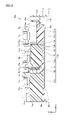
- FIG. FIG. 2 is a schematic cross-sectional view of the semiconductor device shown in FIG. 1 taken along line II-II in FIG.
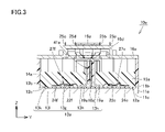
- FIG. 3 is a schematic cross-sectional view of the semiconductor device shown in FIG. 1 taken along line III-III in FIG.
- FIG. 4 is a schematic perspective view of the semiconductor device shown in FIG. 1 when illustration of a later-described lid portion is omitted.
- FIG. 5 is a schematic perspective view of the semiconductor device shown in FIG. 1 in which illustration of a lid, a sealing material, and a frame, which will be described later, is omitted. 6 is a schematic side view of the semiconductor device shown in FIG. 5.
- FIG. FIG. 2 is a schematic cross-sectional view of the semiconductor device shown in FIG. 1 taken along line II-II in FIG.
- FIG. 3 is a schematic cross-sectional view of the semiconductor device shown in FIG. 1 taken along line III-III in
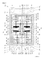
- FIG. 7 is a schematic cross-sectional view of the semiconductor device shown in FIG. 6 taken along line VII-VII in FIG.
- FIG. 8 is a schematic cross-sectional view of the semiconductor device shown in FIG. 7 when illustration of a first electrode, a second electrode, and a third electrode, which will be described later, is omitted.
- FIG. 9 is a schematic cross-sectional view showing only the first electrode, the second electrode and the third electrode in the semiconductor device shown in FIG.
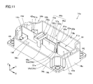
- FIG. 10 schematically shows a part of the circuit diagram of the semiconductor device shown in FIG. 11 is a schematic perspective view of a frame included in the semiconductor device shown in FIG. 1.
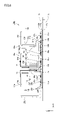
- FIG. FIG. 12 is a schematic cross-sectional view schematically showing part of the semiconductor device shown in FIG. FIG.
- FIG. 13 is a schematic cross-sectional view schematically showing part of the semiconductor device shown in FIG.
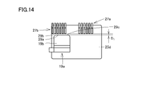
- FIG. 14 is an enlarged view of region R indicated by a dashed line in FIG.
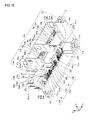
- FIG. 15 is a schematic perspective view showing a state in which a substrate is bonded to a base plate, and semiconductor chips such as a first electrode, a second electrode, a third electrode, and a first semiconductor chip are bonded to a circuit pattern.
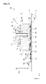
- FIG. 16 is a schematic perspective view showing a state in which the frame is attached to the base plate and the first conductive member and the like are joined.
- FIG. 17 is a schematic perspective view showing a state in which the lid is attached to the frame.
- FIG. 18 is a schematic perspective view showing part of the semiconductor device according to the second embodiment.
- FIG. 19 is a schematic side view of the semiconductor device shown in FIG. 18.
- FIG. FIG. 20 is a schematic cross-sectional view of the semiconductor device shown in FIG. 19 cut along XX-XX in FIG.
- FIG. 21 is a schematic cross-sectional view of the semiconductor device shown in FIG. 20 when illustration of the first electrode, the second electrode, and the third electrode is omitted.
- FIG. 22 is a schematic cross-sectional view showing only the first electrode, the second electrode and the third electrode in the semiconductor device shown in FIG.
- FIG. 23 is a schematic cross-sectional view schematically showing part of the semiconductor device according to the third embodiment.
- FIG. 24 is a schematic cross-sectional view schematically showing part of the semiconductor device according to the fourth embodiment.
- FIG. 25 is a schematic cross-sectional view schematically showing part of the semiconductor device according to the fifth embodiment.
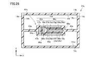
- FIG. 26 is a schematic cross-sectional view schematically showing part of the semiconductor device according to the sixth embodiment.
- a semiconductor device such as the power semiconductor module disclosed in Patent Document 1 requires high insulation between terminals (electrodes). It is desirable that high insulation can be easily achieved without complicated manufacturing processes.
- one object is to provide a semiconductor device that can easily ensure high insulation between electrodes.
- a semiconductor device includes a base plate, a substrate disposed on the base plate and including a first main surface, and a first circuit board, a second circuit board, a third circuit board and a third circuit board which are separated from each other.
- the frame includes insulating ribs projecting from the inner wall surfaces of the side walls. The rib includes an entry that enters between the parallel arranged portions to ensure a creepage distance between the parallel arranged electrodes.
- a current path when current flows in a semiconductor device reaches the first electrode, the first circuit board, the first semiconductor chip, the first conductive member, the second circuit board, and the second electrode. Furthermore, it becomes a second electrode, a third circuit board, a second semiconductor chip, a second conductive member, a fourth circuit board, and a third electrode.
- at least two of the first, second and third electrodes include portions arranged in parallel.
- the frame includes insulating ribs projecting from the inner wall surfaces of the side walls. The rib includes an entry that enters between the parallel arranged portions to ensure a creepage distance between the parallel arranged electrodes.
- the insulation between the portions arranged in parallel can be enhanced by the entrance portion.
- the rib protruding from the inner wall surface is included in the frame, the rib can be arranged when the frame is attached to the base plate. Therefore, it is possible to easily ensure high insulation between the electrodes.
- parallelism rather than having a geometrically strict parallel relationship, for example, one may be inclined with respect to the other by several degrees, specifically within the range of 30 degrees.
- the third electrode may include a first flat plate portion and a second flat plate portion that are arranged in parallel with each other with a space therebetween.
- the second electrode may include a third plate portion disposed between the first plate portion and the second plate portion and spaced apart from each of the first plate portion and the second plate portion.
- the entering portion may enter at least one of between the first flat plate portion and the third flat plate portion and between the second flat plate portion and the third flat plate portion. By doing so, the entering portion enters at least one of between the first flat plate portion and the third flat plate portion and between the second flat plate portion and the third flat plate portion. and between the first and third flat plate portions and between the second and third flat plate portions, high insulation between the electrodes can be easily ensured. .
- the first flat plate portion, the second flat plate portion and the third flat plate portion may be perpendicular to the first main surface.
- the entry portion is positioned between the first flat plate portion and the third flat plate portion and between the second flat plate portion and the third flat plate portion. or one can be easily arranged. Therefore, it is possible to more easily ensure high insulation between the electrodes.
- the vertical does not have a geometrically strict vertical relationship, but for example, one side is inclined to the other side by about several degrees from 90 degrees, specifically within the range of 30 degrees. good too.
- the first electrode may include a seventh flat plate portion.
- the third electrode may include an eighth plate portion arranged parallel to the seventh plate portion.
- the entry portion may be arranged between the seventh flat plate portion and the eighth flat plate portion.
- the seventh flat plate portion and the eighth flat plate portion may be perpendicular to the first main surface.
- the rib may be detachable from the sidewall.
- the rib and the side wall can be manufactured separately, and materials with different CTI (Comparative Tracking Index) can be used according to the creepage distance. Therefore, it becomes easy to change each material.
- CTI Common Tracking Index
- the rib may be integrated with the side wall. By doing so, it is possible to suppress the movement of the ribs due to buoyancy when the sealing material is enclosed. Therefore, reliable insulation can be achieved. Moreover, since it can be molded with one mold, it can be constructed at low cost.
- the rib may be made of thermoplastic resin. By doing so, the rib can be easily manufactured.
- the above semiconductor device may further include a sealing material that insulates a space above the base plate in the area surrounded by the frame.
- the entry may be in contact with the encapsulant.
- the above semiconductor device may further include insulating paper arranged between the portions arranged in parallel.
- the minimum creepage distance can be reduced by using insulating paper with a higher CTI compared to ribs. Therefore, by doing so, it is possible to improve the insulating property even when it is difficult to secure a sufficient creepage distance by using the rib as a resin member.
- a semiconductor device of the present disclosure includes a base plate, a substrate arranged on the base plate and including a first main surface, and a plurality of circuit boards positioned separately from each other, arranged on the first main surface.
- At least two of the first, second and third electrodes include portions that are arranged in parallel.
- the frame includes insulating ribs projecting from the inner wall surfaces of the side walls. The rib includes an entry that enters between the parallel arranged portions to ensure a creepage distance between the parallel arranged electrodes.
- FIG. 1 is a schematic perspective view of a semiconductor device according to Embodiment 1.
- FIG. 2 is a schematic cross-sectional view of the semiconductor device shown in FIG. 1 taken along line II-II in FIG.
- FIG. 3 is a schematic cross-sectional view of the semiconductor device shown in FIG. 1 taken along line III-III in FIG.
- FIG. 4 is a schematic perspective view of the semiconductor device shown in FIG. 1 when illustration of a later-described lid portion is omitted. From the viewpoint of facilitating understanding, FIG. 4 shows a nut, which will be described later.
- FIG. 5 is a schematic perspective view of the semiconductor device shown in FIG.
- FIG. 6 is a schematic side view of the semiconductor device shown in FIG. 5.
- FIG. FIG. 7 is a schematic cross-sectional view of the semiconductor device shown in FIG. 6 taken along line VII-VII in FIG.
- FIG. 7 is a diagram of a substrate viewed in the thickness direction, which will be described later.
- FIG. 7 illustrates a case where a cross section is cut in a region where a sealing material described later is not positioned.
- FIG. 8 is a schematic cross-sectional view of the semiconductor device shown in FIG. 7 when illustration of a first electrode, a second electrode, and a third electrode, which will be described later, is omitted. Note that FIG.
- FIG. 10 is a schematic cross-sectional view showing only the first electrode, the second electrode and the third electrode in the semiconductor device shown in FIG.
- FIG. 10 schematically shows a part of the circuit diagram of the semiconductor device shown in FIG. From the viewpoint of facilitating understanding, FIG. 10 also illustrates capacitors that are connected in parallel with a first semiconductor chip and a second semiconductor chip, which will be described later, and that are not included in the semiconductor device of the present disclosure.
- 11 is a schematic perspective view of a frame included in the semiconductor device shown in FIG. 1.
- FIG. 12 is a schematic cross-sectional view schematically showing part of the semiconductor device shown in FIG.
- FIG. 13 is a schematic cross-sectional view schematically showing part of the semiconductor device shown in FIG.
- FIG. 12 shows the case cut along the XY plane
- FIG. 13 shows the case cut along the XZ plane.
- a semiconductor device 10a includes a plate-like base plate 11a as a base portion, a substrate 12a, a circuit pattern 13a, a frame 14a, and a sealing material 15a. , lid portion 16a, first electrode 17a, second electrode 18a, third electrode 19a, first semiconductor chips 21a, 21b, 21c, 21d, and second semiconductor chips 22a, 22b, 22c, 22d.
- the base plate 11a has a rectangular shape in which the length in the X direction is longer than the length in the Y direction when viewed in the thickness direction (Z direction).
- the base plate 11a is made of metal, for example.
- the base plate 11a includes a first main surface 11b positioned on one side in the thickness direction and a second main surface 11c positioned on the other side in the thickness direction.
- Through holes 11d, 11e, 11f, and 11g are formed through the base plate 11a in the thickness direction at portions near the four corners thereof.
- the through holes 11d, 11e, 11f, and 11g are effectively used together with through holes 14h, 14i, 14j, and 14k, which will be described later, when mounting the semiconductor device 10a at a predetermined installation location.
- a substrate 12a is arranged on the first main surface 11b.
- the substrate 12a has a rectangular shape in which the length in the X direction is longer than the length in the Y direction when viewed in the thickness direction (Z direction).
- the substrate 12a has insulating properties.
- the substrate 12a is made of ceramic, for example.
- the substrate 12a includes a first main surface 12b positioned on one side in the thickness direction and a second main surface 12c positioned on the other side in the thickness direction.
- the second principal surface 12c of the substrate 12a is bonded to the first principal surface 11b of the base plate 11a with a bonding material.
- a circuit pattern 13a is arranged on the first main surface 12b of the substrate 12a.
- the circuit pattern 13a is made of a conductive member, specifically, a copper plate, for example.
- the circuit pattern 13a includes a circuit board (first circuit board) 13b, a circuit board (second circuit board) 13c, a circuit board (third circuit board) 13d, and a circuit board (fourth circuit board) 13e, which are located apart from each other. include.
- the circuit pattern 13a further includes a circuit board (fifth circuit board) 13f, a circuit board (sixth circuit board) 13g, a circuit board (seventh circuit board) 13h, and a circuit board (eighth circuit board) 13i, which are located apart from each other.
- circuit board 13j a circuit board (9th circuit board) 13j, a circuit board (10th circuit board) 13k, a circuit board (11th circuit board) 13l and a circuit board (12th circuit board) 13m.
- the circuit board 13b and the circuit board 13e are arranged separately in the Y direction.
- a circuit board 13c is arranged between the separated circuit boards 13b in the Y direction.
- circuit board 13b, circuit board 13c, circuit board 13d and circuit board 13e, circuit board 13b and circuit board 13e are divided into a plurality of electrically connected circuit boards, specifically two circuit boards. (especially see FIG. 8).
- the circuit board 13f and the circuit board 13h are also divided into a plurality of electrically connected circuit boards, specifically two circuit boards. In this embodiment, the circuit board 13f and the circuit board 13h are arranged separately in the Y direction.
- the area where the circuit boards 13b and 13c are arranged, the area where the circuit boards 13d and 13e are arranged, and the area where the circuit boards 13f, 13g and 13h are arranged are arranged in the X direction. is placed in Specifically, in the X direction, the area where the circuit boards 13b and 13c are arranged is arranged at a position close to the first control terminal 25a, followed by the circuit boards 13f, 13g and 13h. The area where the circuit board 13d and the circuit board 13e are located is then located. That is, in the X direction, the circuit boards 13f, 13g and 13h are arranged between the area where the circuit boards 13b and 13c are arranged and the area where the circuit boards 13d and 13e are arranged. area is placed.
- circuit board 13b, the circuit board 13c, the circuit board 13d, the circuit board 13e, the circuit board 13f, the circuit board 13g, and the circuit board 13h are connected to the first electrode 17a, the second electrode 18a, and the third electrode 18a.
- 19a constitutes a current path.
- Circuit board 13i, circuit board 13j, circuit board 13k, circuit board 13l and circuit board 13m are connected to first semiconductor chip 21a by first control terminal 25a, second control terminal 25b, third control terminal 25c and fourth control terminal 25d. etc.
- the frame 14a is attached to the base plate 11a. Specifically, it is attached to the first main surface 11b of the base plate 11a with an adhesive (not shown).
- the frame 14a has a rectangular shape in which the length in the X direction is longer than the length in the Y direction when viewed in the thickness direction of the substrate 12a.
- the frame 14a includes four side walls 14b, 14c, 14d, 14e surrounding the outer periphery of the substrate 12a.
- the substrate 12a is arranged in a space 14f surrounded by the four side walls 14b, 14c, 14d, 14e of the frame 14a.
- Four through holes 14h, 14i, 14j, and 14k penetrating in the Z direction are formed in portions near the four corners of the frame 14a.
- the through holes 14h, 14i, 14j, and 14k are arranged so as to match the positions of the four through holes 11d, 11e, 11f, and 11g of the base plate 11a when the frame 14a is attached to the base plate 11a. .
- the first control terminal 25a, the second control terminal 25b, the third control terminal 25c, and the fourth control terminal 25d are inserted into the side wall portion 14d of the frame 14a.
- the material of the frame 14a a material having high insulation and strength is used, and specifically, PPS (Polyphenylene sulfide) resin, for example, is used.
- PPS Polyphenylene sulfide
- Such a resin is a thermoplastic resin and has good moldability, excellent insulation properties, moisture resistance, heat resistance, and high strength.
- PBT Polybutylene Terephthalate
- the frame 14a includes ribs 41a. A specific configuration of the frame 14a will be described in detail later.
- the sealing material 15a covers the substrate 12a.
- the sealing material 15a fills a part of the space 14f inside the frame 14a.
- the sealing material 15a is arranged with a gap from the lid portion 16a.
- the sealing material 15a is in contact with the side surface of the substrate 12a and part of the first major surface 12b. Specifically, the sealing material 15a is in contact with the side surface of the substrate 12a and the first main surface 12b in the portion where the semiconductor chip 21a and the like are not arranged.
- the sealing material 15a electrically insulates the space on the side surface of the substrate 12a and the space above the substrate 12a in the area surrounded by the frame 14a.
- the encapsulant 15a is used for the components arranged on the substrate 12a, more specifically, the first semiconductor chips 21a, 21b, 21c and 21d and the second semiconductor chips 22a, 22b, 22c and 22d.
- sealing 28b, 28c, 28d and 28e The members on the base plate 11a are fixed by the sealing material 15a.
- a resin having high insulation and heat resistance is adopted as the material of the sealing material 15a.
- a thermosetting resin such as an epoxy resin, a phenol resin, a silicone resin, or the like is employed as the sealing material 15a.
- the lid portion 16a is plate-shaped.
- the lid portion 16a has a rectangular shape in which the length in the X direction is longer than the length in the Y direction when viewed in the thickness direction of the substrate 12a, and four cut corners are provided near the four corners. It has a shape with a notch.
- the lid portion 16a is adhered to the frame 14a with an adhesive (not shown).
- the lid portion 16a is arranged so as to cover the opening 14g of the frame 14a.
- Three terminal blocks 16b, 16c, and 16d are formed on the lid portion 16a and are spaced apart in the longitudinal direction.
- the terminal blocks 16b, 16c, and 16d are spaced apart in the X direction.
- Three through holes 16e, 16f, and 16g are formed in the lid portion 16a so as to penetrate in the thickness direction (Z direction).
- the three through holes 16e, 16f, 16g are formed at positions where the three terminal blocks 16b, 16c, 16d are provided, respectively.
- the three through-holes 16e, 16f, and 16g correspond to the first electrode 17a and the second electrodes 17a and 16g, respectively, in a state in which third regions 17d, 18d, and 19d, which will be described later, are not bent when the lid portion 16a is attached to the frame 14a.
- the electrode 18a and the third electrode 19a are arranged at positions where parts of the electrode 18a and the third electrode 19a penetrate.
- a first electrode 17a, a second electrode 18a, and a third electrode 19a are electrically connected to external electrodes (not shown) at positions where the terminal blocks 16b, 16c, and 16d are provided in the lid portion 16a.
- Nuts 16h, 16i, and 16j are outserted or press-fitted as fastening members used for this purpose. From the viewpoint of facilitating understanding, the nuts 16h, 16i, and 16j are illustrated in FIG.
- the material of the lid portion 16a for example, the same material as that of the frame body 14a, specifically PPS resin or PBT resin, is adopted.
- the semiconductor chips 21e and 21f, the sixth semiconductor chips 22e and 22f, the seventh semiconductor chips 23e and 23f and the eighth semiconductor chips 24e and 24f are wide bandgap semiconductor chips, respectively.
- first semiconductor chips 21a, 21b, 21c, 21d, second semiconductor chips 22a, 22b, 22c, 22d, third semiconductor chips 23a, 23b, 23c, 23d, fourth semiconductor chips 24a, 24b, 24c , 24d, fifth semiconductor chips 21e, 21f, sixth semiconductor chips 22e, 22f, seventh semiconductor chips 23e, 23f, and eighth semiconductor chips 24e, 24f each include a semiconductor layer made of SiC (silicon carbide). .
- the semiconductor layer may be made of Si (silicon) or GaN (gallium nitride), for example.
- the first semiconductor chips 21a, 21b, 21c, 21d, the second semiconductor chips 22a, 22b, 22c, 22d, the fifth semiconductor chips 21e, 21f, and the sixth semiconductor chips 22e, 22f each have a metal-oxide-semiconductor field effect structure. type transistor (MOSFET).
- MOSFET type transistor
- the first semiconductor chips 21a, 21b, 21c, 21d, the second semiconductor chips 22a, 22b, 22c, 22d, the fifth semiconductor chips 21e, 21f, and the sixth semiconductor chips 22e, 22f are vertical type semiconductor chips. is a transistor chip.
- the first semiconductor chips 21a, 21b, 21c, 21d, the second semiconductor chips 22a, 22b, 22c, 22d, the fifth semiconductor chips 21e, 21f, and the sixth semiconductor chips 22e, 22f are arranged in the thickness direction (Z direction).
- ) is a transistor chip through which current flows.
- the first semiconductor chips 21a, 21b, 21c and 21d, the second semiconductor chips 22a, 22b, 22c and 22d, the fifth semiconductor chips 21e and 21f and the sixth semiconductor chips 22e and 22f are switching elements, respectively.
- the first semiconductor chips 21a, 21b, 21c, and 21d are arranged on the circuit board 13b. Specifically, the first semiconductor chips 21a and 21b are arranged on the circuit board 13b closer to the side wall portion 14b of the divided circuit boards 13b. The first semiconductor chips 21c and 21d are arranged on the circuit board 13b closer to the side wall portion 14c of the divided circuit boards 13b. The first semiconductor chips 21a and 21b are spaced apart in the X direction. The first semiconductor chips 21c and 21d are spaced apart in the X direction. The first semiconductor chips 21a and 21c are spaced apart in the Y direction. The first semiconductor chips 21b and 21d are spaced apart in the Y direction.
- the first semiconductor chips 21a, 21b, 21c, and 21d are bonded to the circuit board 13b with a conductive bonding material (not shown), thereby connecting the drain electrode pads of the first semiconductor chips 21a, 21b, 21c, and 21d. , and the circuit board 13b.
- the second semiconductor chips 22a, 22b, 22c, 22d are arranged on the circuit board 13d. Specifically, the second semiconductor chips 22a and 22b are arranged on the circuit board 13d at positions close to the side wall portion 14b. The second semiconductor chips 22c and 22d are arranged on the circuit board 13d at positions close to the side wall portion 14c. The second semiconductor chips 22a and 22b are spaced apart in the X direction. The second semiconductor chips 22c and 22d are spaced apart in the X direction. The second semiconductor chips 22a and 22c are spaced apart in the Y direction. The second semiconductor chips 22b and 22d are spaced apart in the Y direction.
- the second semiconductor chips 22a, 22b, 22c, and 22d are bonded to the circuit board 13d with a conductive bonding material (not shown), thereby forming drain electrode pads of the second semiconductor chips 22a, 22b, 22c, and 22d. , and the circuit board 13d.
- the fifth semiconductor chips 21e and 21f are arranged on the circuit board 13f. Specifically, the fifth semiconductor chip 21e is arranged on the circuit board 13f closer to the side wall portion 14b among the divided circuit boards 13f. The fifth semiconductor chip 21f is arranged on the circuit board 13f closer to the side wall part 14c among the divided circuit boards 13f. The fifth semiconductor chips 21e and 21f are spaced apart in the Y direction. The fifth semiconductor chips 21e and 21f are bonded to the circuit board 13f with a conductive bonding material (not shown), thereby electrically connecting the drain electrode pads of the fifth semiconductor chips 21e and 21f and the circuit board 13f. connected to The sixth semiconductor chips 22e and 22f are arranged on the circuit board 13g.
- the sixth semiconductor chip 22e is arranged on the circuit board 13g at a position close to the side wall portion 14b.
- the sixth semiconductor chip 22f is arranged on the circuit board 13g at a position close to the side wall portion 14c.
- the sixth semiconductor chips 22e and 22f are spaced apart in the Y direction.
- the sixth semiconductor chips 22e and 22f are bonded to the circuit board 13g with a conductive bonding material (not shown), thereby electrically connecting the drain electrode pads of the sixth semiconductor chips 22e and 22f and the circuit board 13g. connected to
- the third semiconductor chips 23a, 23b, 23c and 23d, the fourth semiconductor chips 24a, 24b, 24c and 24d, the seventh semiconductor chips 23e and 23f and the eighth semiconductor chips 24e and 24f are Schottky barrier diodes (SBD). be.
- the third semiconductor chips 23a, 23b, 23c, 23d, the fourth semiconductor chips 24a, 24b, 24c, 24d, the seventh semiconductor chips 23e, 23f, and the eighth semiconductor chips 24e, 24f have a thickness of It is a diode chip through which current flows in the direction (Z direction).
- the third semiconductor chips 23a, 23b, 23c, 23d are arranged on the circuit board 13b. Specifically, the third semiconductor chips 23a and 23b are arranged on the circuit board 13b closer to the side wall portion 14b of the divided circuit board 13b. The third semiconductor chips 23c and 23d are arranged on the circuit board 13b closer to the side wall portion 14c of the divided circuit boards 13b. Further, the third semiconductor chips 23a and 23b are respectively arranged between the side wall portion 14b and the first semiconductor chips 21a and 21b in the Y direction. The third semiconductor chips 23c and 23d are respectively arranged between the side wall portion 14c and the first semiconductor chips 21c and 21d in the Y direction. The third semiconductor chips 23a and 23b are spaced apart in the X direction.
- the third semiconductor chips 23c and 23d are spaced apart in the X direction.
- the third semiconductor chips 23a and 23c are spaced apart in the Y direction.
- the third semiconductor chips 23b and 23d are spaced apart in the Y direction.
- the third semiconductor chips 23a, 23b, 23c, and 23d are bonded to the circuit board 13b with a conductive bonding material (not shown), thereby forming cathode electrode pads of the third semiconductor chips 23a, 23b, 23c, and 23d. , and the circuit board 13b.
- the fourth semiconductor chips 24a, 24b, 24c, 24d are arranged on the circuit board 13d. Specifically, the fourth semiconductor chips 24a and 24b are arranged on the circuit board 13d at positions close to the side wall portion 14b. Further, the fourth semiconductor chips 24c and 24d are arranged on the circuit board 13d at positions close to the side wall portion 14c. Also, the fourth semiconductor chips 24a and 24b are arranged between the side wall portion 14b and the second semiconductor chips 22a and 22b in the Y direction, respectively. The fourth semiconductor chips 24c and 24d are respectively arranged between the side wall portion 14c and the second semiconductor chips 22c and 22d in the Y direction. The fourth semiconductor chips 24a and 24b are spaced apart in the X direction.
- the fourth semiconductor chips 24c and 24d are spaced apart in the X direction.
- the fourth semiconductor chips 24a and 24c are spaced apart in the Y direction.
- the fourth semiconductor chips 24b and 24d are spaced apart in the Y direction.
- the fourth semiconductor chips 24a, 24b, 24c, and 24d are bonded to the circuit board 13d with a conductive bonding material (not shown), thereby forming cathode electrode pads of the fourth semiconductor chips 24a, 24b, 24c, and 24d. , and the circuit board 13d.
- the seventh semiconductor chips 23e and 23f are arranged on the circuit board 13f. Specifically, the seventh semiconductor chip 23e is arranged on the circuit board 13f closer to the side wall part 14b among the divided circuit boards 13f. The seventh semiconductor chip 23f is arranged on the circuit board 13f closer to the side wall part 14c among the divided circuit boards 13f. Also, the seventh semiconductor chip 23e is arranged between the side wall portion 14b and the fifth semiconductor chip 21e in the Y direction. The seventh semiconductor chip 23f is arranged between the sidewall portion 14c and the fifth semiconductor chip 21f in the Y direction. The seventh semiconductor chips 23e and 23f are spaced apart in the Y direction.
- the seventh semiconductor chips 23e and 23f are bonded to the circuit board 13f by a conductive bonding material (not shown), thereby electrically connecting the cathode electrode pads of the seventh semiconductor chips 23e and 23f and the circuit board 13f. connected to The eighth semiconductor chips 24e and 24f are arranged on the circuit board 13g. Specifically, the eighth semiconductor chip 24e is arranged on the circuit board 13g at a position close to the side wall portion 14b. The eighth semiconductor chip 24f is arranged on the circuit board 13g at a position close to the side wall portion 14c. The eighth semiconductor chip 24e is arranged between the side wall portion 14b and the sixth semiconductor chip 22e in the Y direction.
- the eighth semiconductor chip 24f is arranged between the side wall portion 14c and the sixth semiconductor chip 22f in the Y direction.
- the eighth semiconductor chips 24e and 24f are spaced apart in the Y direction.
- the eighth semiconductor chips 24e and 24f are bonded to the circuit board 13g with a conductive bonding material (not shown), thereby electrically connecting the cathode electrode pads of the eighth semiconductor chips 24e and 24f and the circuit board 13g. connected to
- first conductive members 26a, 26b, 26c, 26d, the second conductive members 27a, 27b, 27c, 27d, the third conductive members 26e, 26f, and the fourth conductive members 27e, 27f are solid. It is a cylindrical, electrically conductive aluminum wire. First conductive members 26a, 26b, 26c, 26d, second conductive members 27a, 27b, 27c, 27d, third conductive members 26e, 26f, fourth conductive members 27e, 27f, wires 28a, 28b, 28c, 28d, 28e are respectively bonded to each member by wire bonding using a bonding tool.
- the first conductive members 26a, 26b, 26c, 26d, the second conductive members 27a, 27b, 27c, 27d, the third conductive members 26e, 26f, and the fourth conductive members 27e, 27f are conductive copper wires.
- a plate-like conductive member made of aluminum or copper may be used.
- Aluminum and copper may be pure aluminum or pure copper, or may be aluminum alloys or copper alloys. In the case of plate-like members, they are joined by soldering, for example.
- the first conductive members 26a, 26b, 26c, 26d electrically connect the first semiconductor chips 21a, 21b, 21c, 21d and the circuit board 13c. Specifically, the first conductive members 26a, 26b, 26c, 26d electrically connect the source electrode pads of the first semiconductor chips 21a, 21b, 21c, 21d and the circuit board 13c. The first conductive members 26a, 26b, 26c and 26d electrically connect the source electrode pads of the first semiconductor chips 21a, 21b, 21c and 21d and the anode electrode pads of the third semiconductor chips 23a, 23b, 23c and 23d. connect to.
- the second conductive members 27a, 27b, 27c, 27d electrically connect the second semiconductor chips 22a, 22b, 22c, 22d and the circuit board 13e. Specifically, the second conductive members 27a, 27b, 27c, 27d electrically connect the source electrode pads of the second semiconductor chips 22a, 22b, 22c, 22d and the circuit board 13e. The second conductive members 27a, 27b, 27c and 27d electrically connect the source electrode pads of the second semiconductor chips 22a, 22b, 22c and 22d and the anode electrode pads of the fourth semiconductor chips 24a, 24b, 24c and 24d. connect to.
- the third conductive members 26e, 26f electrically connect the fifth semiconductor chips 21e, 21f and the circuit board 13g. Specifically, the third conductive members 26e and 26f electrically connect the source electrode pads of the fifth semiconductor chips 21e and 21f and the circuit board 13g. The third conductive members 26e and 26f electrically connect the source electrode pads of the fifth semiconductor chips 21e and 21f and the anode electrode pads of the seventh semiconductor chips 23e and 23f.
- the fourth conductive members 27e, 27f electrically connect the sixth semiconductor chips 22e, 22f and the circuit board 13h. Specifically, the fourth conductive members 27e and 27f electrically connect the source electrode pads of the sixth semiconductor chips 22e and 22f and the circuit board 13h. The fourth conductive members 27e and 27f electrically connect the source electrode pads of the sixth semiconductor chips 22e and 22f and the anode electrode pads of the eighth semiconductor chips 24e and 24f.
- first control terminal 25a and the circuit board 13i are connected by a wire 28a.
- the second control terminal 25b and the circuit board 13j are connected by a wire 28b.
- the third control terminal 25c and the circuit board 13k are connected by a wire 28c.
- the fourth control terminal 25d and the circuit board 13l are connected by a wire 28d.
- the circuit board 13l and the circuit board 13m are connected by a wire 28e.
- the gate electrode pads of the first semiconductor chips 21a, 21b, 21c, 21d and the fifth semiconductor chips 21e, 21f and the circuit board 13i are electrically connected by wires.
- the source electrode pads of the first semiconductor chips 21a, 21b, 21c, 21d and the fifth semiconductor chips 21e, 21f and the circuit board 13j are electrically connected by wires.
- the gate electrode pads of the second semiconductor chips 22a, 22b, 22c, 22d and the sixth semiconductor chips 22e, 22f and the circuit board 13k are electrically connected by wires.
- the source electrode pads of the second semiconductor chips 22a, 22b, 22c, 22d and the sixth semiconductor chips 22e, 22f and the circuit board 13l or the circuit board 13m are electrically connected by wires.
- Each of the first electrode 17a, the second electrode 18a and the third electrode 19a has a plate shape.
- the first electrode 17a, the second electrode 18a and the third electrode 19a are conductive.
- the first electrode 17a, the second electrode 18a and the third electrode 19a are each made of a bent copper plate.
- the first electrode 17a, the second electrode 18a and the third electrode 19a are respectively arranged on the circuit pattern 13a.
- the first electrode 17a, the second electrode 18a, and the third electrode 19a are arranged separately from the side wall portions 14b, 14c, 14d, and 14e that constitute the frame 14a.
- the first electrode 17a, the second electrode 18a and the third electrode 19a are formed with through-holes 17e, 18e and 19e extending in the thickness direction in portions exposed from the lid portion 16a.
- the first electrode 17a is a so-called P terminal
- the second electrode 18a is a so-called O terminal
- the third electrode 19a is a so-called N terminal.
- the first electrode 17a is connected to the circuit board 13b of the circuit pattern 13a.
- the first electrode 17a includes a first region 17b connected to the circuit board 13b and a second region 17c extending in the direction intersecting the first main surface 12b, which is connected to the first region 17b and extending in the Z direction in this embodiment. and a third region 17d that extends in a direction that intersects the direction in which the second region 17c extends and that is exposed from the sealing material 15a.
- the third region 17d includes a portion extending in the X direction.
- the first region 17b is bonded to the circuit board 13b with a conductive bonding material such as solder. Parts of the first region 17b and the second region 17c are located inside the sealing material 15a.
- the third region 17d includes a region exposed to the outside, that is, a region exposed from the lid portion 16a.
- the above-described through hole 17e is formed in the third region 17d.
- the first electrode 17a is also connected to the circuit board 13f. Thus, the first electrode 17a is electrically connected to the circuit boards 13b and 13f.
- the second electrode 18a is connected to the circuit board 13c and the circuit board 13d of the circuit pattern 13a.
- the second electrode 18a extends in a first region 18b connected to the circuit board 13c and the circuit board 13d, and in a direction connecting the first region 18b and crossing the first main surface 12b, which is the Z direction in this embodiment. It includes a second region 18c, and a third region 18d that is continuous with the second region 18c and extends in a direction that intersects the direction in which the second region 18c extends and that is exposed from the sealing material 15a.
- the third region 18d includes a portion extending in the X direction.
- the first region 18b is joined to each of the circuit board 13c and the circuit board 13d with a conductive joining material such as solder. Parts of the first region 18b and the second region 18c are located inside the sealing material 15a.
- the third region 18d includes a region exposed to the outside, that is, a region exposed from the lid portion 16a. The above-described through hole 18e is formed in the third region 18d.
- the second electrode 18a is also connected to the circuit board 13g. Thus, the second electrode 18a is electrically connected to the circuit boards 13c, 13d and 13g.
- the circuit board 13c and the circuit board 13d are electrically connected by the plate-shaped second electrode 18a. Therefore, in the electrical path between the circuit boards 13c and 13d, the wiring resistance can be reduced as compared with the case where the circuit boards 13c and 13d are connected by wiring such as wires and circuit patterns 13a. can be done.
- the third electrode 19a is connected to the circuit board 13e of the circuit pattern 13a.
- the third electrode 19a includes a first region 19b connected to the circuit board 13e, and a second region 19c extending in the direction intersecting the first main surface 12b and extending in the Z direction in this embodiment. and a third region 19d that is continuous with the second region 19c and extends in a direction intersecting the direction in which the second region 19c extends and that is exposed from the sealing material 15a.
- the third region 19d includes a portion extending in the X direction.
- the first region 19b is joined to the circuit board 13e by a conductive joining material such as solder. Parts of the first region 19b and the second region 19c are located inside the sealing material 15a.
- the third region 19d includes a region exposed to the outside, that is, a region exposed from the lid portion 16a.
- the above-described through hole 19e is formed in the third region 19d.
- the third electrode 19a is also connected to the circuit board 13h. Thus, the third electrode 19a is electrically connected to the circuit boards 13e and 13h.
- the third electrode 19a includes a first flat plate portion 19f and a second flat plate portion 19g which are arranged in parallel with a space therebetween.
- the first flat plate portion 19f and the second flat plate portion 19g are spaced apart in the Y direction.
- the first flat plate portion 19f and the second flat plate portion 19g are perpendicular to the first major surface 12b.
- the first flat plate portion 19f and the second flat plate portion 19g are each parallel to the XZ plane.
- the second electrode 18a includes a third flat plate portion 18f.
- the third flat plate portion 18f is perpendicular to the first major surface 12b.
- the third flat plate portion 18f is parallel to the XZ plane.
- the third flat plate portion 18f is arranged between the first flat plate portion 19f and the second flat plate portion 19g and spaced apart from each of the first flat plate portion 19f and the second flat plate portion 19g. That is, the first flat plate portion 19f, the second flat plate portion 19g, and the third flat plate portion 18f constitute parallel flat plates.
- the second electrode 18a includes a first portion 18g arranged parallel to and spaced from the third electrode 19a.
- the first portion 18g is the third flat plate portion 18f.
- the first electrode 17a includes a seventh flat plate portion 17f (see FIG. 6 in particular).
- the seventh flat plate portion 17f is perpendicular to the first main surface 12b.
- the seventh flat plate portion 17f is parallel to the YZ plane.
- the third electrode 19a includes an eighth flat plate portion 19h.
- the eighth flat plate portion 19h is perpendicular to the first major surface 12b.
- the eighth flat plate portion 19h is parallel to the YZ plane. That is, the seventh flat plate portion 17f and the eighth flat plate portion 19h constitute parallel flat plates.
- the first electrode 17a includes a third portion 17g arranged parallel to and spaced from the third electrode 19a.
- the third portion 17g is the seventh flat plate portion 17f.
- the second electrode 18a includes a ninth flat plate portion 18h.
- the ninth flat plate portion 18h is perpendicular to the first major surface 12b.
- the ninth flat plate portion 18h is parallel to the YZ plane.
- FIG. 14 is an enlarged view of region R indicated by a dashed line in FIG.
- the gap 29a between the Y - direction end 29c of and is indicated by D1 in FIG.
- the gap D1 is 1 mm or more in this embodiment. Alternatively, the gap D1 is 5 mm or more.
- the frame 14a includes ribs 41a.
- the ribs 41a protrude from the inner wall surfaces 14n, 14o of the side wall portions 14d, 14e.
- the rib 41a is provided so as to extend in the X direction from the inner wall surface 14n of the side wall portion 14d toward the opposing inner wall surface 14o.
- the rib 41a is provided from the side wall portion 14d to the side wall portion 14e. That is, the rib 41a is provided in the frame 14a so as to have a beam shape connecting the side wall portion 14d and the side wall portion 14e.
- the frame 14a is configured to be less likely to vibrate, and vibration resistance can be improved.
- the rib 41a is integrated with the side wall portions 14d and 14e.
- the ribs 41a are also made of the thermoplastic resin described above. By doing so, the rib 41a can be easily manufactured.
- the frame body 14a can be molded with one mold, it can be constructed at a low cost.
- the rib 41a is connected to the inner wall surface 14n of the side wall portion 14d and extends straight in the X direction
- the second protrusion portion 43a is connected to the inner wall surface 14o of the side wall portion 14e and extends straight in the X direction.
- a central portion 44a connected to each of the first protrusion 42a and the second protrusion 43a.
- Central portion 44a is not in contact with inner wall surface 14l of side wall portion 14b and inner wall surface 14m of side wall portion 14c.
- the central portion 44a includes a first support portion 45a that supports the first electrode 17a and the third electrode 19a, and a second support portion 46a that supports the second electrode 18a and the third electrode 19a.
- the first support portion 45a is connected to the first projecting portion 42a.
- the second support portion 46a is connected to the second projecting portion 43a.
- the first support portion 45a and the second support portion 46a are arranged side by side in the X direction.
- a first guide hole 47a and a second guide hole 48a are formed in the first support portion 45a.
- the first guide hole 47a and the second guide hole 48a respectively penetrate in the thickness direction (Z direction) of the substrate 12a.
- the first guide hole 47a and the second guide hole 48a are spaced apart in the X direction.
- the wall surfaces of the first guide hole 47a and the second guide hole 48a are rectangular along the contours of the first electrode 17a and the third electrode 19a, respectively, when viewed in the thickness direction of the substrate 12a.
- the first guide hole 47a is configured to be able to pass through the third region 17d of the first electrode 17a before bending.
- the second guide hole 48a is configured to be able to pass through the third region 19d of the third electrode 19a before bending.
- a portion located between the first guide hole 47a and the second guide hole 48a serves as an entrance portion 49a that enters between the first electrode 17a and the third electrode 19a.
- a first guide groove 51a and a second guide groove 52a are formed in the second support portion 46a.
- the first guide groove 51a is formed so as to be recessed in the Z direction.
- the second support portion 46a includes an eleventh flat plate portion 53a, a twelfth flat plate portion 54a, and a first connection portion 55a.
- the eleventh flat plate portion 53a and the twelfth flat plate portion 54a are arranged in parallel with a gap in the Y direction.
- the first connecting portion 55a is provided to connect the Z-direction end of the eleventh flat plate portion 53a and the Z-direction end of the twelfth flat plate portion 54a.
- the first guide groove 51a is formed between an eleventh flat plate portion 53a and a twelfth flat plate portion 54a that are spaced apart in the Y direction.
- a portion of the third flat plate portion 18f of the second electrode 18a is arranged in the first guide groove 51a.
- the first flat plate portion 19f of the third electrode 19a is arranged on the facing surface 56a side of the eleventh flat plate portion 53a facing the inner wall surface 14m of the side wall portion 14c.
- the eleventh flat plate portion 53a serves as an entrance portion 58a that enters between the second electrode 18a and the third electrode 19a.
- the second flat plate portion 19g of the third electrode 19a is arranged on the facing surface 57a side of the twelfth flat plate portion 54a facing the inner wall surface 14l of the side wall portion 14b.
- the twelfth flat plate portion 54a serves as an entrance portion 59a that enters between the second electrode 18a and the third electrode 19a.
- the second guide groove 52a is formed so as to be recessed in the Y direction.
- the second support portion 46a includes a thirteenth flat plate portion 61a, a fourteenth flat plate portion 62a, and a second connection portion 63a.
- the thirteenth flat plate portion 61a and the fourteenth flat plate portion 62a are arranged in parallel with an interval in the X direction.
- the second connecting portion 63a is provided to connect the Y-direction end of the thirteenth flat plate portion 61a and the Y-direction end of the fourteenth flat plate portion 62a.
- the second guide groove 52a is formed between a thirteenth flat plate portion 61a and a fourteenth flat plate portion 62a that are spaced apart in the X direction.
- a portion of the ninth flat plate portion 18h is arranged in the second guide groove 52a.
- the entry portions 49a, 58a, 59a included in the rib 41a are configured to reach positions where the sealing material 15a is arranged. That is, each of the entry portions 49a, 58a, 59a is in contact with the sealing material 15a as shown in FIG.
- the current path when the current flows in the semiconductor device 10a is from the first electrode 17a to the circuit board 13b, the first semiconductor chips 21a, 21b, 21c and 21d, the first conductive members 26a, 26b, 26c and 26d, the circuit board 13c, It reaches the second electrode 18a. Further, the second electrode 18a, the circuit board 13d, the second semiconductor chips 22a, 22b, 22c, 22d, the second conductive members 27a, 27b, 27c, 27d, the circuit board 13e, and the third electrode 19a.
- the circuit board 13f As a current path, from the first electrode 17a to the circuit board 13f, the fifth semiconductor chips 21e, 21f, the third conductive members 26e, 26f, the circuit board 13g, the second electrode 18a, the second electrode 18a, the circuit There is also a path to plate 13h, fourth conductive members 27e, 27f, sixth semiconductor chip 22e, 22f, circuit board 13g, and third electrode 19a.
- a capacitor 101 such as a smoothing capacitor is connected in parallel with first semiconductor chips 21a, 21b, 21c and 21d and second semiconductor chips 22a, 22b, 22c and 22d. There is At this time, a closed circuit is formed between the capacitor 101 and the first semiconductor chips 21a, 21b, 21c and 21d and the second semiconductor chips 22a, 22b, 22c and 22d.
- the path of this closed circuit is from the first electrode 17a to the circuit board 13b, the first semiconductor chips 21a, 21b, 21c, 21d, the first conductive members 26a, 26b, 26c, 26d, the circuit board 13c, the second It becomes a path to the electrode 18a, the circuit board 13d, the second semiconductor chips 22a, 22b, 22c, 22d, the second conductive members 27a, 27b, 27c, 27d, the circuit board 13e, and the third electrode 19a.
- a high di/dt occurs in this closed circuit at the time of switching.
- the inductance In the surge voltage, if the inductance is large, a high surge voltage is generated when a high di/dt occurs, and is applied to the first semiconductor chips 21a, 21b, 21c, 21d and the second semiconductor chips 22a, 22b, 22c, 22d. will be Such a state may damage the first semiconductor chips 21a, 21b, 21c, 21d and the second semiconductor chips 22a, 22b, 22c, 22d. Therefore, suppression of surge voltage is required. If the inductance can be reduced in the current path from the first electrode 17a to the third electrode 19a, the surge voltage can be suppressed.
- fifth semiconductor chips 21e and 21f can be arranged in parallel with the first semiconductor chips 21a, 21b, 21c and 21d.
- sixth semiconductor chips 22e and 22f can be arranged in parallel with the second semiconductor chips 22a, 22b, 22c and 22d.
- the second electrode 18a current flows from the first region 18b to the third region 18d via the second region 18c.
- the third flat plate portion 18f which is the first portion 18g in the second region 18c
- the third electrode 19a current flows from the first region 19b to the third region 19d via the second region 19c.
- first electrode 17a current flows from the third region 17d to the first region 17b via the second region 17c.
- second region 17c current flows in the direction opposite to arrow Z , as indicated by arrow V3.
- third electrode 19a current flows from the first region 19b to the third region 19d via the second region 19c.
- eighth flat plate portion 19h in the second region 19c current flows in the direction of arrow Z as indicated by arrow V4.
- the second electrode 18a includes a first portion 18g arranged parallel to and spaced from the third electrode 19a. Therefore, by making the direction of the current flowing through the third electrode 19a and the direction of the current flowing through the second electrode 18a opposite to each other in the portion arranged in parallel, the current in the second electrode 18a and the third electrode 19a cancels the magnetic flux produced when the current flows through, and the mutual inductance subtracts the inductance of the current path. Therefore, it is possible to reduce the inductance of the semiconductor device 10a.
- the third electrode 19a includes a first flat plate portion 19f and a second flat plate portion 19g that are spaced apart and arranged in parallel.
- the second electrode 18a is a third flat plate portion 18f arranged between the first flat plate portion 19f and the second flat plate portion 19g and spaced apart from the first flat plate portion 19f and the second flat plate portion 19g. including.
- the third flat plate portion 18f serves as the first portion 18g. Therefore, between the third flat plate portion 18f and the first flat plate portion 19f and the second flat plate portion 19g arranged in parallel, the direction of the current flowing through the third electrode 19a and the direction of the current flowing through the second electrode 18a are different.
- the inductance of the semiconductor device 10a can be further reduced.
- the first electrode 17a includes a third portion 17g arranged parallel to and spaced from the third electrode 19a. Therefore, by making the direction of the current flowing through the first electrode 17a and the direction of the current flowing through the third electrode 19a opposite in the portions arranged in parallel, the inside of the first electrode 17a and the third electrode 19a Mutual inductance offsets the inductance of the path by canceling the magnetic flux created when the current flows. Therefore, the inductance of the semiconductor device 10a can be further reduced.
- the first electrode 17a includes a seventh flat plate portion 17f.
- the third electrode 19a includes an eighth flat plate portion 19h arranged parallel to the seventh flat plate portion 17f.
- the seventh flat plate portion 17f serves as the third portion 17g. Therefore, between the seventh flat plate portion 17f and the eighth flat plate portion 19h, which are arranged in parallel, the direction of the current flowing through the first electrode 17a and the direction of the current flowing through the third electrode 19a are reversed. cancels the magnetic flux generated when the current flows in the first electrode 17a and the third electrode 19a, and the mutual inductance subtracts the inductance of the path. Therefore, the inductance of the semiconductor device 10a can be further reduced.
- the frame 14a includes insulating ribs 41a projecting from the inner wall surfaces 14n, 14o of the side wall portions 14d, 14e.
- the rib 41a enters between the parallel-arranged portion, specifically, the second electrode 18a and the third electrode 19a, and extends along the surface between the parallel-arranged second electrode 18a and the third electrode 19a. It includes entrances 58a and 59a that ensure a distance.
- the rib 41a includes an entering portion 49a which enters between the first electrode 17a and the third electrode 19a to secure a creeping distance between the first electrode 17a and the third electrode 19a arranged in parallel.
- the insulation between the parts arranged in parallel can be enhanced by the entrances 49a, 58a, 59a.
- the ribs 41a projecting from the inner wall surfaces 14l and 14o are included in the frame 14a, the ribs 41a can be arranged when the frame 14a is attached to the base plate 11a. Therefore, it is possible to easily ensure high insulation between the electrodes.
- the entering portions 58a, 59a enter between the first flat plate portion 19f and the third flat plate portion 18f and between the second flat plate portion 19g and the third flat plate portion 18f. Therefore, the entering portions 58a, 59a easily separate the second electrode 18a and the third electrode between the first flat plate portion 19f and the third flat plate portion 18f and between the second flat plate portion 19g and the third flat plate portion 18f. High insulation between 19a can be ensured.
- the entrance portion 49a is arranged between the seventh flat plate portion 17f and the eighth flat plate portion 19h. Therefore, the entering portion 49a can be easily arranged between the seventh flat plate portion 17f of the first electrode 17a and the eighth flat plate portion 19h of the third electrode 19a which are arranged in parallel. Therefore, it is possible to easily ensure high insulation between the first electrode 17a and the third electrode 19a.
- the base plate 11a is prepared.
- the substrate 12a is joined to the base plate 11a using a conductive joining material such as plate solder or paste solder, and the first electrode 17a, the second electrode 18a, the third electrode 19a and the third electrode 19a are attached to the circuit pattern 13a.
- a conductive joining material such as plate solder or paste solder
- the first electrode 17a, the second electrode 18a, the third electrode 19a and the third electrode 19a are attached to the circuit pattern 13a.
- Each semiconductor chip such as the semiconductor chip 21a is bonded.
- the first electrode 17a, the second electrode 18a, and the third electrode 19a are in a state where the respective third regions 17d, 18d, and 19d are not bent.
- FIG. 15 schematically shows a state in which a substrate 12a is bonded to a base plate 11a, and semiconductor chips such as a first electrode 17a, a second electrode 18a, a third electrode 19a, and a first semiconductor chip 21a are bonded to a circuit pattern 13a. It is a perspective view.
- the frame 14a is attached to the base plate 11a using an adhesive.
- a first control terminal 25a, a second control terminal 25b, a third control terminal 25c, and a fourth control terminal 25d are attached in advance to the frame 14a.
- the seventh flat plate portion 17f of the first electrode 17a is accommodated in the first guide hole 47a
- the eighth flat plate portion 19h of the third electrode 19a is accommodated in the second guide hole 48a
- the third flat plate portion 18f of the second electrode is accommodated in the first guide groove 51a
- the ninth flat plate portion 18h of the second electrode is accommodated in the second guide groove 52a, and attached to the base plate 11a.
- the facing surface 56a is arranged to face the first flat plate portion 19f of the third electrode 19a
- the facing surface 57a is arranged to face the second flat plate portion 19g of the third electrode 19a.
- the first flat plate portion 19f, the second flat plate portion 19g and the third flat plate portion 18f are perpendicular to the first main surface 12b. Therefore, when attaching the frame 14a to the base plate 11a, the entrance portions 58a, 59a are positioned between the first flat plate portion 19f and the third flat plate portion 18f and between the second flat plate portion 19g and the third flat plate portion 18f. It can be easily arranged. Therefore, it is possible to more easily ensure high insulation between the second electrode 18a and the third electrode 19a.
- the seventh flat plate portion 17f and the eighth flat plate portion 19h are perpendicular to the first major surface 12b. Therefore, when the frame 14a is attached to the base plate 11a, the entrance portion 49a can be easily arranged between the seventh flat plate portion 17f and the eighth flat plate portion 19h. Therefore, it is possible to more easily ensure high insulation between the first electrode 17a and the third electrode 19a.
- FIG. 16 is a schematic perspective view showing a state in which the frame 14a is attached to the base plate 11a and the first conductive member 26a and the like are joined.
- the semiconductor device 10a of the present disclosure when viewed in the thickness direction of the substrate 12a, the first electrode 17a, the second electrode 18a, and the third electrode 19a covered with the sealing material 15a and the first conductive member There is a gap 29a between 26a, 26b, 26c, 26d, second conductive members 27a, 27b, 27c, 27d, third conductive members 26e, 26f and fourth conductive members 27e, 27f.
- Such a semiconductor device 10a includes a first electrode 17a, a second electrode 18a, and a third electrode 19a covered with a sealing material 15a, and first conductive members 26a, 26b, 19a and 19a, which are covered with a sealing material 15a when viewed in the thickness direction of the substrate 12a.
- the bonding with the electrode 18a and the third electrode 19a can be performed simultaneously.
- the first conductive members 26a, 26b, 26c and 26d, the second conductive members 27a, 27b, 27c and 27d, the third conductive members 26e and 26f and the third conductive members 26e and 26f are bonded using a bonding tool. It is possible to reduce the risk of the bonding tool interfering with the first electrode 17a, the second electrode 18a and the third electrode 19a when wiring is performed by the fourth conductive members 27e and 27f. Therefore, productivity can be improved.
- the space 14f surrounded by the frame 14a is filled with the liquid sealing material 15a from the opening 14g side.
- the sealing material 15a is filled so that the sealing material 15a and the entrance portions 49a, 58a, 59a are in contact with each other even after the sealing material 15a is cured.
- the ribs 41a are integrated with the side wall portions 14d and 14e. Therefore, it is possible to suppress the movement of the rib 41a due to buoyancy when the sealing material 15a is enclosed. Therefore, reliable insulation can be achieved.
- the first flat plate portion 19f, the second flat plate portion 19g and the third flat plate portion 18f are perpendicular to the first main surface 12b. Therefore, when the sealing material 15a is filled, air bubbles trapped in the sealing material 15a are prevented from accumulating in the lower regions of the first flat plate portion 19f, the second flat plate portion 19g, and the third flat plate portion 18f. be able to. Therefore, it is possible to avoid the possibility that air bubbles are accumulated in the sealing material 15a, suppress the deterioration of the insulation performance, and improve the reliability of the semiconductor device 10a.
- the seventh flat plate portion 17f and the eighth flat plate portion 19h are perpendicular to the first major surface 12b. Therefore, when enclosing the sealing material 15a, it is possible to prevent the voids that have been entrapped during enclosing the sealing material 15a from accumulating in the lower regions of the seventh flat plate portion 17f and the eighth flat plate portion 19h. Therefore, it is possible to avoid the possibility that voids are accumulated in the sealing material 15a, suppress the deterioration of the insulation performance, and improve the reliability of the semiconductor device 10a.
- FIG. 17 is a schematic perspective view showing a state in which the lid portion 16a is attached to the frame 14a.
- first electrode 17a, second electrode 18a and third electrode 19a Referring to FIG. 17, first electrode 17a, second electrode 18a and third electrode 19a.
- the third region 18d that is not folded and the third region 19d of the third electrode 19a that is not bent pass through the through holes 16e, 16f, and 16g of the lid portion 16a, respectively. Attached to body 14a.
- the portions of the first electrode 17a, the second electrode 18a and the third electrode 19a exposed from the lid portion 16a are bent 90 degrees in the X direction.
- the exposed portions of the first electrode 17a, the second electrode 18a and the third electrode 19a follow the outer shape of the terminal blocks 16b, 16c and 16d, and the opening portions of the through holes 17e, 18e and 19e are aligned with the nuts 16h and 16h. It is configured to match the respective screw holes of 16i and 16j.
- the semiconductor device 10a shown in FIG. 1 is manufactured.
- FIG. 18 is a schematic perspective view showing part of the semiconductor device according to the second embodiment.
- illustration of a lid, a sealing material, and a frame is omitted.
- 19 is a schematic side view of the semiconductor device shown in FIG. 18.
- FIG. 20 is a schematic cross-sectional view of the semiconductor device shown in FIG. 19 cut along XX-XX in FIG.
- FIG. 21 is a schematic cross-sectional view of the semiconductor device shown in FIG. 20 when illustration of the first electrode, the second electrode, and the third electrode is omitted.
- FIG. 22 is a schematic cross-sectional view showing only the first electrode, the second electrode and the third electrode in the semiconductor device shown in FIG.
- the semiconductor device of Embodiment 2 differs from that of Embodiment 1 in that the configurations of the first electrode, the second electrode and the third electrode are different. Further, in the second embodiment, circuit board 13e and circuit board 13h are not divided.
- a semiconductor device 10b of the second embodiment includes a first electrode 17j, a second electrode 18j and a third electrode 19j.
- the first electrode 17j includes a fourth flat plate portion 17k and a fifth flat plate portion 17l that are arranged in parallel with a space therebetween.
- the fourth flat plate portion 17k and the fifth flat plate portion 17l are spaced apart in the Y direction.
- the fourth flat plate portion 17k and the fifth flat plate portion 17l are perpendicular to the first major surface 12b.
- the fourth flat plate portion 17k and the fifth flat plate portion 17l are each parallel to the XZ plane.
- the second electrode 18j includes a sixth flat plate portion 18k.
- the sixth flat plate portion 18k is perpendicular to the first major surface 12b.
- the sixth flat plate portion 18k is parallel to the XZ plane.
- the sixth flat plate portion 18k is arranged between the fourth flat plate portion 17k and the fifth flat plate portion 17l and is spaced apart from each of the fourth flat plate portion 17k and the fifth flat plate portion 17l. That is, the fourth flat plate portion 17k, the fifth flat plate portion 17l, and the sixth flat plate portion 18k constitute parallel flat plates.
- the second electrode 18j includes a second portion 18l arranged parallel to and spaced from the first electrode 17j.
- the second portion 18l is the sixth flat plate portion 18k.
- the first electrode 17j includes a seventh flat plate portion 17m (see FIG. 19 in particular).
- the seventh flat plate portion 17m is perpendicular to the first main surface 12b.
- the seventh flat plate portion 17m is parallel to the YZ plane.
- the third electrode 19j includes an eighth flat plate portion 19k.
- the eighth flat plate portion 19k is perpendicular to the first major surface 12b.
- the eighth flat plate portion 19k is parallel to the YZ plane. That is, the seventh flat plate portion 17m and the eighth flat plate portion 19k constitute parallel flat plates.
- the first electrode 17j includes a third portion 17n arranged parallel to and spaced from the third electrode 19j.
- the third portion 17n is the seventh flat plate portion 17m.
- the second electrode 18j includes the ninth flat plate portion 18m.
- the ninth flat plate portion 18m is perpendicular to the first major surface 12b.
- the ninth flat plate portion 18m is parallel to the YZ plane.
- the first guide hole, the second guide hole, the first A frame 14a including ribs provided with guide grooves and second guide grooves is used.
- the second electrode 18j includes a second portion 18l arranged parallel to and spaced from the first electrode 17j. Therefore, by making the direction of the current flowing through the third electrode 19j and the direction of the current flowing through the second electrode 18j opposite to each other in the portion arranged in parallel, the current in the second electrode 18j and the third electrode 19j cancels the magnetic flux produced when the current flows through, and the mutual inductance subtracts the inductance of the current path. Therefore, it is possible to reduce the inductance of the semiconductor device 10b.
- the first electrode 17j includes a fourth flat plate portion 17k and a fifth flat plate portion 17l that are arranged in parallel with a space therebetween.
- the second electrode 18j is a sixth flat plate portion 18k arranged between the fourth flat plate portion 17k and the fifth flat plate portion 17l and spaced apart from each of the fourth flat plate portion 17k and the fifth flat plate portion 17l. including.
- the sixth flat plate portion 18k is the second portion 18l. Therefore, between the sixth flat plate portion 18k, the fourth flat plate portion 17k, and the fifth flat plate portion 17l, which are arranged in parallel, the magnetic flux generated when the current flows in the second electrode 18j and the first electrode 17j is Cancellation, mutual inductance subtracts the inductance of the path. Therefore, the inductance of the semiconductor device 10b can be further reduced.
- the fourth flat plate portion 17k, the fifth flat plate portion 17l and the sixth flat plate portion 18k are perpendicular to the first main surface 12b. Therefore, when the sealing material 15a is filled, air bubbles caught in the sealing material 15a are prevented from accumulating in the lower regions of the fourth flat plate portion 17k, the fifth flat plate portion 17l, and the sixth flat plate portion 18k. be able to. Therefore, it is possible to avoid the possibility that air bubbles are accumulated in the sealing material 15a, suppress the deterioration of the insulation performance, and improve the reliability of the semiconductor device 10b.
- the entry portions 58a and 59a are positioned between the fourth flat plate portion 17k and the sixth flat plate portion 18k and between the fifth flat plate portion 17l and the sixth flat plate portion 18k. It can be easily arranged. Therefore, it is possible to more easily ensure high insulation between the second electrode 18j and the third electrode 19j.
- the first electrode 17j includes the seventh flat plate portion 17m.
- the third electrode 19j includes an eighth flat plate portion 19k arranged parallel to the seventh flat plate portion 17m. Therefore, between the seventh flat plate portion 17m and the eighth flat plate portion 19k that are arranged in parallel, the direction of the current flowing through the first electrode 17j and the direction of the current flowing through the third electrode 19j should be opposite. cancels the magnetic flux generated when the current flows in the first electrode 17j and the third electrode 19j, and mutual inductance subtracts the inductance of the path. Therefore, the inductance of the semiconductor device 10b can be further reduced.
- the seventh flat plate portion 17m and the eighth flat plate portion 19k are perpendicular to the first major surface 12b. Therefore, it is possible to prevent air bubbles trapped in the sealing material 15a from accumulating in the lower regions of the seventh flat plate portion 17m and the eighth flat plate portion 19k when the sealing material 15a is filled. Therefore, it is possible to avoid the possibility that air bubbles are accumulated in the sealing material 15a, suppress the deterioration of the insulation performance, and improve the reliability of the semiconductor device 10b.
- the entrance portion 49a can be easily arranged between the seventh flat plate portion 17m and the eighth flat plate portion 19k. Therefore, it is possible to more easily ensure high insulation between the first electrode 17j and the third electrode 19j.
- FIG. 23 is a schematic cross-sectional view schematically showing part of the semiconductor device according to the third embodiment.
- FIG. 23 is a cross section including the frame, first electrode, second electrode and third electrode.
- the semiconductor device of the third embodiment differs from that of the first embodiment in that the structure of the frame is different.
- rib 41b is detachable from side walls 14d and 14e. That is, the rib 41b is a separate member from the side wall portions 14b, 14c, 14d, and 14e. Notches 14q and 14r into which the ribs 41b are fitted are formed in the side wall portions 14d and 14e, respectively. Each of the first projecting portion 42a and the second projecting portion 43a of the rib 41b is formed longer in the X direction than in the case shown in the first embodiment.
- the rib 41b is attached to the side walls 14d, 14e by fitting the ends of the first protrusion 42a and the second protrusion 43a into the notches 14q, 14r.
- the rib 41b and the side wall portions 14b, 14c, 14d, and 14e can be manufactured separately, and materials with different CTI (Comparative Tracking Index) can be used according to the creepage distance. can be done. Therefore, it becomes easy to change the material of each of the side walls 14b, 14c, 14d, 14e and the rib 41b.
- CTI Common Tracking Index
- the frame body 14p may be constructed by fitting the first projecting portion 42a and the second projecting portion 43a of the rib 41b into.
- FIG. 24 is a schematic cross-sectional view schematically showing part of the semiconductor device according to the fourth embodiment.
- FIG. 24 is a cross section including the frame, first electrode, second electrode and third electrode.
- the semiconductor device of Embodiment 4 is different from that of Embodiment 1 in that the first, second and third electrodes are integrated with the frame.
- rib 41a is formed integrally with first electrode 17a, second electrode 18a and third electrode 19a.
- a first support portion 45a of the rib 41a is formed with a first accommodation portion 47b that accommodates the first electrode 17a and a second accommodation portion 48b that accommodates the third electrode 19a.
- the second supporting portion 46a of the rib 41a has a third accommodating portion 51b for accommodating the second electrode 18a, and the third electrode 19a, specifically, the first flat plate portion 19f and the second flat plate portion of the third electrode 19a.
- a first fitting portion 56b and a second fitting portion 57b are formed in which 19g is fitted.
- the frame 14s, the first electrode 17a, the second electrode 18a and the third electrode 19a can be integrated, so that the number of parts can be reduced and the insulation between the electrodes can be ensured. can be achieved.
- FIG. 25 is a schematic cross-sectional view schematically showing part of the semiconductor device according to the fifth embodiment.
- FIG. 25 is a cross section including the frame, first electrode, second electrode and third electrode.
- the semiconductor device of the fifth embodiment differs from that of the first embodiment in that the frame body includes insulating paper.
- frame body 14t included in the semiconductor device of the present embodiment has a portion between portions where at least two of first electrode 17a, second electrode 18a and third electrode 19a are arranged in parallel.
- Insulating papers 64a, 65a, 66a arranged in the .
- the insulating paper 64a is arranged so as to be attached to the wall surface of the first guide hole 47a on the side where the entrance portion 49a is located. That is, the insulating paper 64a is arranged between the first electrode 17a and the entrance portion 49a in the X direction.
- the insulating paper 65a is arranged so as to be attached to the opposing surface 56a.
- the insulating paper 65a is arranged between the first flat plate portion 19f of the third electrode 19a and the facing surface 56a in the Y direction.
- the insulating paper 66a is arranged so as to be attached to the opposing surface 57a. That is, the insulating paper 66a is arranged between the second flat plate portion 19g of the third electrode 19a and the facing surface 57a in the Y direction.
- Each of the insulating papers 64a, 65a, 66a is attached by adhesive, for example.
- the minimum creepage distance can be reduced by using the insulating papers 64a, 65a, and 66a with higher CTI than the rib 41a. Therefore, by doing so, it is possible to improve the insulating property even when it is difficult to secure a sufficient creepage distance by using the rib 41a as a resin member.
- FIG. 26 is a schematic cross-sectional view schematically showing part of the semiconductor device according to the sixth embodiment.
- FIG. 26 is a cross section including the frame, first electrode, second electrode and third electrode.
- the semiconductor device of Embodiment 6 is different from that of Embodiment 5 in that the frame including the insulating paper and the first electrode and the like are integrated.
- frame body 14u included in the semiconductor device of the present embodiment has a portion between portions where at least any two of first electrode 17a, second electrode 18a and third electrode 19a are arranged in parallel.
- Insulating papers 64a, 65a, 66a arranged in the .
- the rib 41a is formed integrally with the first electrode 17a, the second electrode 18a, the third electrode 19a, and the insulating papers 64a, 65a, 66a.
- an insulating paper 64a is arranged between the first accommodating portion 47b that accommodates the first electrode 17a and the second accommodating portion 48b that accommodates the third electrode 19a. .
- the insulating paper 64a is embedded in the entrance portion 49a.
- an insulating paper 65a is arranged between the third accommodating portion 51b that accommodates the second electrode 18a and the facing surface 56a. That is, the insulating paper 65a is embedded in the entrance portion 58a.
- an insulating paper 66a is arranged between the third housing portion 51b housing the second electrode 18a and the facing surface 57a. That is, the insulating paper 66a is embedded in the entrance portion 59a.
- the frame 14u, the first electrode 17a, the second electrode 18a, the third electrode 19a, and the insulating papers 64a, 65a, 66a can be integrated in this manner, the number of parts can be reduced. Reliable insulation between the electrodes can be achieved, and insulation can be improved even when it is difficult to ensure a sufficient creepage distance by using the rib 41a as a resin member.
- any one of the insulating papers 64a, 65a, and 66a may be provided as needed.
- the ribs are made of thermoplastic resin, but the present invention is not limited to this. and a part of the rib may be made of an insulating member such as ceramic.
- the third region of each of the first electrode, the second electrode, and the third electrode is bent 90 degrees in the portion exposed from the lid.
- the portion exposed from the lid portion may be configured to extend in a shape as it is without being bent, for example, in a direction perpendicular to the first main surface.
- another member may be attached by welding or the like to constitute the first electrode or the like.
- circuit board 13b, circuit board 13c, circuit board 13d, and circuit board 13e may be divided into a plurality of electrically connected circuit boards. good. By doing so, the degree of freedom in designing the shape of the circuit pattern 13a can be increased.
- a semiconductor device of the present disclosure includes a base plate, a substrate arranged on the base plate and including a first main surface, and a plurality of circuit boards positioned separately from each other, arranged on the first main surface.
- At least two of the first, second and third electrodes include portions that are arranged in parallel.
- the frame includes insulating ribs projecting from the inner wall surfaces of the side walls. The rib includes an entry that enters between the parallel arranged portions to ensure a creepage distance between the parallel arranged electrodes.
Landscapes
- Structures Or Materials For Encapsulating Or Coating Semiconductor Devices Or Solid State Devices (AREA)
Abstract
半導体装置は、ベース板と、基板と、回路パターンと、板状の第1電極と、板状の第2電極と、板状の第3電極と、第1半導体チップと、第2半導体チップと、ベース板に取り付けられ、基板の外周を取り囲む側壁部を含む枠体14と、を備える。第1電極、第2電極および第3電極のうちの少なくとも2つは、平行に配置されている部分を含む。枠体は、側壁部の内壁面から突出する絶縁性のリブを含む。リブは、平行に配置されている部分の間に進入し、平行に配置された電極間の沿面距離を確保する進入部を含む。
Description
本開示は、半導体装置に関するものである。
本出願は、2021年1月22日出願の日本出願第2021-8836号に基づく優先権を主張し、前記日本出願に記載された全ての記載内容を援用するものである。
半導体素子が基板上に配置された半導体装置が知られている(例えば、特許文献1参照)。特許文献1に開示の半導体装置は、パワー半導体モジュールであり、正極電源端子と、負極電源端子と、出力端子と、を含む。
本開示に従った半導体装置は、ベース板と、ベース板上に配置され、第1の主面を含む基板と、それぞれ離れて位置する第1回路板、第2回路板、第3回路板および第4回路板を含み、第1の主面上に配置される回路パターンと、回路パターン上に配置され、第1回路板と接続される板状の第1電極と、回路パターン上に配置され、第2回路板および第3回路板と接続される板状の第2電極と、回路パターン上に配置され、第4回路板と接続される板状の第3電極と、第1回路板上に配置される第1半導体チップと、第3回路板上に配置される第2半導体チップと、第1半導体チップと第2回路板とを電気的に接続する第1導電部材と、第2半導体チップと第4回路板とを電気的に接続する第2導電部材と、ベース板に取り付けられ、基板の外周を取り囲む側壁部を含む枠体と、を備える。第1電極、第2電極および第3電極のうちの少なくとも2つは、平行に配置されている部分を含む。枠体は、側壁部の内壁面から突出する絶縁性のリブを含む。リブは、平行に配置されている部分の間に進入し、平行に配置された電極間の沿面距離を確保する進入部を含む。
[本開示が解決しようとする課題]
特許文献1に開示されるパワー半導体モジュールのような半導体装置においては、端子(電極)間における高い絶縁性が求められる。高い絶縁性を確保するに際し、煩雑な製造工程を経ることなく、容易に実現できることが望ましい。
特許文献1に開示されるパワー半導体モジュールのような半導体装置においては、端子(電極)間における高い絶縁性が求められる。高い絶縁性を確保するに際し、煩雑な製造工程を経ることなく、容易に実現できることが望ましい。
そこで、容易に電極間の高い絶縁性を確保することができる半導体装置を提供することを目的の1つとする。
[本開示の効果]
上記半導体装置によれば、容易に電極間の高い絶縁性を確保することができる。
上記半導体装置によれば、容易に電極間の高い絶縁性を確保することができる。
[本開示の実施形態の説明]
最初に本開示の実施態様を列記して説明する。本開示に係る半導体装置は、ベース板と、ベース板上に配置され、第1の主面を含む基板と、それぞれ離れて位置する第1回路板、第2回路板、第3回路板および第4回路板を含み、第1の主面上に配置される回路パターンと、回路パターン上に配置され、第1回路板と接続される板状の第1電極と、回路パターン上に配置され、第2回路板および第3回路板と接続される板状の第2電極と、回路パターン上に配置され、第4回路板と接続される板状の第3電極と、第1回路板上に配置される第1半導体チップと、第3回路板上に配置される第2半導体チップと、第1半導体チップと第2回路板とを電気的に接続する第1導電部材と、第2半導体チップと第4回路板とを電気的に接続する第2導電部材と、ベース板に取り付けられ、基板の外周を取り囲む側壁部を含む枠体と、を備える。第1電極、第2電極および第3電極のうちの少なくとも2つは、平行に配置されている部分を含む。枠体は、側壁部の内壁面から突出する絶縁性のリブを含む。リブは、平行に配置されている部分の間に進入し、平行に配置された電極間の沿面距離を確保する進入部を含む。
最初に本開示の実施態様を列記して説明する。本開示に係る半導体装置は、ベース板と、ベース板上に配置され、第1の主面を含む基板と、それぞれ離れて位置する第1回路板、第2回路板、第3回路板および第4回路板を含み、第1の主面上に配置される回路パターンと、回路パターン上に配置され、第1回路板と接続される板状の第1電極と、回路パターン上に配置され、第2回路板および第3回路板と接続される板状の第2電極と、回路パターン上に配置され、第4回路板と接続される板状の第3電極と、第1回路板上に配置される第1半導体チップと、第3回路板上に配置される第2半導体チップと、第1半導体チップと第2回路板とを電気的に接続する第1導電部材と、第2半導体チップと第4回路板とを電気的に接続する第2導電部材と、ベース板に取り付けられ、基板の外周を取り囲む側壁部を含む枠体と、を備える。第1電極、第2電極および第3電極のうちの少なくとも2つは、平行に配置されている部分を含む。枠体は、側壁部の内壁面から突出する絶縁性のリブを含む。リブは、平行に配置されている部分の間に進入し、平行に配置された電極間の沿面距離を確保する進入部を含む。
半導体装置において電流が流れる際の電流経路は、第1電極、第1回路板、第1半導体チップ、第1導電部材、第2回路板、第2電極に至る。さらに、第2電極、第3回路板、第2半導体チップ、第2導電部材、第4回路板、そして第3電極となる。本開示の半導体装置によると、第1電極、第2電極および第3電極のうちの少なくとも2つは、平行に配置されている部分を含む。そして、枠体は、側壁部の内壁面から突出する絶縁性のリブを含む。リブは、平行に配置されている部分の間に進入し、平行に配置された電極間の沿面距離を確保する進入部を含む。したがって、平行に配置されている部分を含む第1電極、第2電極および第3電極のうちの少なくとも2つにおいて、平行に配置されている部分の間の絶縁性を進入部により高めることができる。この場合、内壁面から突出するリブは、枠体に含まれているため、枠体のベース板への取り付け時にリブを配置することができる。よって、容易に電極間の高い絶縁性を確保することができる。平行については、幾何学的に厳密な平行の関係を有するのではなく、例えば一方に対して他方が数度程度、具体的には30度の範囲内で傾いていてもよい。
上記半導体装置において、第3電極は、間隔をあけてそれぞれ平行に配置される第1平板部および第2平板部を含んでもよい。第2電極は、第1平板部と第2平板部との間であって、第1平板部および第2平板部のそれぞれと間隔をあけて配置される第3平板部を含んでもよい。進入部は、第1平板部と第3平板部との間および第2平板部と第3平板部との間のうちの少なくともいずれか1つに進入してもよい。このようにすることにより、進入部は、第1平板部と第3平板部との間および第2平板部と第3平板部との間のうちの少なくともいずれか1つに進入しているため、第1平板部と第3平板部との間および第2平板部と第3平板部との間のうちの少なくともいずれか1つにおいて、容易に電極間の高い絶縁性を確保することができる。
上記半導体装置において、第1平板部、第2平板部および第3平板部は、第1の主面に対して垂直であってもよい。このようにすることにより、枠体をベース板に取り付ける際に、進入部を第1平板部と第3平板部との間および第2平板部と第3平板部との間のうちの少なくともいずれか1つに容易に配置しやすくすることができる。よって、より容易に電極間の高い絶縁性を確保することができる。ここで、垂直について、幾何学的に厳密な垂直の関係を有するのではなく、例えば一方に対して他方が90度に対して数度程度、具体的には30度の範囲内で傾いていてもよい。
上記半導体装置において、第1電極は、第7平板部を含んでもよい。第3電極は、第7平板部と平行に配置される第8平板部を含んでもよい。進入部は、第7平板部と第8平板部との間に配置されてもよい。このようにすることにより、平行に配置される第1電極の第7平板部と第3電極の第8平板部との間に進入する進入部を容易に配置することができる。したがって、容易に第1電極と第3電極との間の高い絶縁性を確保することができる。
上記半導体装置において、第7平板部および第8平板部は、第1の主面に対して垂直であってもよい。このようにすることにより、枠体をベース板に取り付ける際に、進入部を第7平板部と第8平板部との間に容易に配置しやすくすることができる。よって、より容易に電極間の高い絶縁性を確保することができる。
上記半導体装置において、リブは、側壁部と着脱可能であってもよい。このようにすることにより、リブと側壁部とを別途製造することができ、沿面距離に応じて比較トラッキング指数(CTI(Comparative Tracking Index))の異なる材質を使うことができる。したがって、それぞれの材質を変更することが容易となる。
上記半導体装置において、リブは、側壁部と一体であってもよい。このようにすることにより、封止材を封入した際に、リブが浮力で動くことを抑制することができる。よって、確実な絶縁を図ることができる。また、一つの金型で成形できるため、安価に構成することができる。
上記半導体装置において、リブは、熱可塑性樹脂から構成されていてもよい。このようにすることにより、リブを容易に製造することができる。
上記半導体装置において、枠体に取り囲まれた領域のうちのベース板上の空間を絶縁する封止材をさらに備えてもよい。進入部は、封止材と接触していてもよい。このようにすることにより、十分な沿面距離を確保することができ、より確実に電極間の絶縁を図ることができる。
上記半導体装置において、平行に配置されている部分の間に配置される絶縁紙をさらに備えてもよい。リブと比較してCTIの高い絶縁紙を用いることで最小沿面距離を小さくすることができる。したがって、このようにすることにより、リブを樹脂部材として沿面距離が十分に確保することが困難な場合においても、絶縁性の向上を図ることができる。
なお、本開示において、回路パターン上の回路板や半導体チップの位置や導電部材の位置については、必ずしも上述の場合に限定されない。例えば、以下のような実施態様でもよい。本開示の半導体装置は、ベース板と、ベース板上に配置され、第1の主面を含む基板と、それぞれ離れて位置する複数の回路板を含み、第1の主面上に配置される回路パターンと、回路パターン上に配置され、回路板の一つと接続される板状の第1電極と、回路パターン上に配置され、回路板の二つと接続される板状の第2電極と、回路パターン上に配置され、回路板の一つと接続される板状の第3電極と、回路板上に配置される第1半導体チップと、回路板上に配置される第2半導体チップと、ベース板に取り付けられ、基板の外周を取り囲む側壁部を含む枠体と、を備える。第1電極、第2電極および第3電極のうちの少なくとも2つは、平行に配置されている部分を含む。枠体は、側壁部の内壁面から突出する絶縁性のリブを含む。リブは、平行に配置されている部分の間に進入し、平行に配置された電極間の沿面距離を確保する進入部を含む。
[本開示の実施形態の詳細]
次に、本開示の半導体装置の一実施形態を、図面を参照しつつ説明する。以下の図面において同一または相当する部分には同一の参照符号を付しその説明は繰り返さない。
次に、本開示の半導体装置の一実施形態を、図面を参照しつつ説明する。以下の図面において同一または相当する部分には同一の参照符号を付しその説明は繰り返さない。
(実施の形態1)
本開示の実施の形態1における半導体装置の構成について説明する。図1は、実施の形態1における半導体装置の概略斜視図である。図2は、図1に示す半導体装置を図1中のII-IIで切断した場合の概略断面図である。図3は、図1に示す半導体装置を図1中のIII-IIIで切断した場合の概略断面図である。図4は、図1に示す半導体装置において、後述する蓋部の図示を省略した場合の概略斜視図である。なお、理解を容易にする観点から、図4において後述するナットを図示している。図5は、図1に示す半導体装置において、後述する蓋部、封止材および枠体の図示を省略した場合の概略斜視図である。図6は、図5に示す半導体装置の概略側面図である。図7は、図6に示す半導体装置を図6中のVII-VIIで切断した場合の概略断面図である。図7は、後述する基板の厚さ方向に見た図である。なお、図7は、後述する封止材が位置しない領域における断面で切断した場合を図示している。図8は、図7に示す半導体装置において、後述する第1電極、第2電極および第3電極の図示を省略した場合の概略断面図である。なお、図2は、図7中の一点鎖線を含む平面で切断した場合の断面に対応する。また、図3は、図7中の二点鎖線を含む平面で切断した場合の断面に対応する。図9は、図7に示す半導体装置において、第1電極、第2電極および第3電極のみを図示した場合の概略断面図である。図10は、図1に示す半導体装置の回路図の一部を概略的に示す図である。なお、図10においては、理解を容易にする観点から、後述する第1半導体チップおよび第2半導体チップと並列接続される、本開示の半導体装置に含まれない構成のコンデンサも図示している。図11は、図1に示す半導体装置に含まれる枠体の概略斜視図である。図12は、図1に示す半導体装置の一部を模式的に示す概略断面図である。図13は、図1に示す半導体装置の一部を模式的に示す概略断面図である。図12は、X-Y平面で切断した場合を示し、図13は、X-Z平面で切断した場合を示す。
本開示の実施の形態1における半導体装置の構成について説明する。図1は、実施の形態1における半導体装置の概略斜視図である。図2は、図1に示す半導体装置を図1中のII-IIで切断した場合の概略断面図である。図3は、図1に示す半導体装置を図1中のIII-IIIで切断した場合の概略断面図である。図4は、図1に示す半導体装置において、後述する蓋部の図示を省略した場合の概略斜視図である。なお、理解を容易にする観点から、図4において後述するナットを図示している。図5は、図1に示す半導体装置において、後述する蓋部、封止材および枠体の図示を省略した場合の概略斜視図である。図6は、図5に示す半導体装置の概略側面図である。図7は、図6に示す半導体装置を図6中のVII-VIIで切断した場合の概略断面図である。図7は、後述する基板の厚さ方向に見た図である。なお、図7は、後述する封止材が位置しない領域における断面で切断した場合を図示している。図8は、図7に示す半導体装置において、後述する第1電極、第2電極および第3電極の図示を省略した場合の概略断面図である。なお、図2は、図7中の一点鎖線を含む平面で切断した場合の断面に対応する。また、図3は、図7中の二点鎖線を含む平面で切断した場合の断面に対応する。図9は、図7に示す半導体装置において、第1電極、第2電極および第3電極のみを図示した場合の概略断面図である。図10は、図1に示す半導体装置の回路図の一部を概略的に示す図である。なお、図10においては、理解を容易にする観点から、後述する第1半導体チップおよび第2半導体チップと並列接続される、本開示の半導体装置に含まれない構成のコンデンサも図示している。図11は、図1に示す半導体装置に含まれる枠体の概略斜視図である。図12は、図1に示す半導体装置の一部を模式的に示す概略断面図である。図13は、図1に示す半導体装置の一部を模式的に示す概略断面図である。図12は、X-Y平面で切断した場合を示し、図13は、X-Z平面で切断した場合を示す。
図1~図13を参照して、実施の形態1における半導体装置10aは、ベース部としての板状のベース板11aと、基板12aと、回路パターン13aと、枠体14aと、封止材15aと、蓋部16aと、第1電極17aと、第2電極18aと、第3電極19aと、第1半導体チップ21a,21b,21c,21dと、第2半導体チップ22a,22b,22c,22dと、第3半導体チップ23a,23b,23c,23dと、第4半導体チップ24a,24b,24c,24dと、第5半導体チップ21e,21fと、第6半導体チップ22e,22fと、第7半導体チップ23e,23fと、第8半導体チップ24e,24fと、第1制御端子25aと、第2制御端子25bと、第3制御端子25cと、第4制御端子25dと、第1導電部材26a,26b,26c,26dと、第2導電部材27a,27b,27c,27dと、第3導電部材26e,26fと、第4導電部材27e,27fと、ワイヤ28a,28b,28c,28d,28eと、を含む。
本実施形態においては、ベース板11aは、厚さ方向(Z方向)に見て、X方向の長さの方がY方向の長さよりも長い矩形状である。ベース板11aは、例えば金属製である。ベース板11aは、厚さ方向の一方に位置する第1の主面11bと、厚さ方向の他方に位置する第2の主面11cと、を含む。ベース板11aの四隅に近い部分には、それぞれ厚さ方向に貫通する貫通孔11d,11e,11f,11gが形成されている。貫通孔11d,11e,11f,11gは、後述する貫通孔14h,14i,14j,14kと共に、半導体装置10aを所定の設置個所に取り付ける際に有効に利用される。
第1の主面11b上には、基板12aが配置されている。本実施形態においては、基板12aは、厚さ方向(Z方向)に見て、X方向の長さの方がY方向の長さよりも長い矩形状である。基板12aは、絶縁性を有する。基板12aは、例えばセラミック製である。基板12aは、厚さ方向の一方に位置する第1の主面12bと、厚さ方向の他方に位置する第2の主面12cと、を含む。基板12aの第2の主面12cは、接合材によりベース板11aの第1の主面11bに接合されている。
基板12aの第1の主面12b上には、回路パターン13aが配置されている。回路パターン13aは、導電性を有する部材、具体的には例えば銅板から構成されている。回路パターン13aは、それぞれ離れて位置する回路板(第1回路板)13b、回路板(第2回路板)13c、回路板(第3回路板)13dおよび回路板(第4回路板)13eを含む。回路パターン13aはさらに、それぞれ離れて位置する回路板(第5回路板)13f、回路板(第6回路板)13g、回路板(第7回路板)13h、回路板(第8回路板)13i、回路板(第9回路板)13j、回路板(第10回路板)13k、回路板(第11回路板)13lおよび回路板(第12回路板)13mを含む。回路板13bおよび回路板13eはそれぞれ、Y方向に分離されて配置されている。分離する回路板13bのY方向の間に、回路板13cが配置される。回路板13b、回路板13c、回路板13dおよび回路板13eのうち、回路板13bおよび回路板13eは、電気的に接続される複数の回路板、具体的には2つの回路板に分割されている(特に図8参照)。なお、回路板13fおよび回路板13hについても、電気的に接続される複数の回路板、具体的には2つの回路板に分割されている。本実施形態においては、回路板13fおよび回路板13hはそれぞれ、Y方向に分離されて配置されている。
回路板13bおよび回路板13cが配置される領域と、回路板13dおよび回路板13eが配置される領域と、回路板13f、回路板13gおよび回路板13hが配置される領域は、X方向に並んで配置される。具体的には、X方向において、第1制御端子25aに近い位置に回路板13bおよび回路板13cが配置される領域が配置され、次に、回路板13f、回路板13gおよび回路板13hが配置される領域が配置され、次に、回路板13dおよび回路板13eが配置される領域が配置される。すなわち、X方向において、回路板13bおよび回路板13cが配置される領域と回路板13dおよび回路板13eが配置される領域との間に、回路板13f、回路板13gおよび回路板13hが配置される領域が配置される。
半導体装置10aの動作時において、回路板13b、回路板13c、回路板13d、回路板13e、回路板13f、回路板13gおよび回路板13hは、第1電極17a、第2電極18aおよび第3電極19aと共に電流経路を構成する。回路板13i、回路板13j、回路板13k、回路板13lおよび回路板13mは、第1制御端子25a、第2制御端子25b、第3制御端子25cおよび第4制御端子25dによる第1半導体チップ21a等の制御に用いられる。
枠体14aは、ベース板11aに取り付けられる。具体的には、ベース板11aの第1の主面11b上に図示しない接着剤により取り付けられる。本実施形態においては、枠体14aは、基板12aの厚さ方向に見て、X方向の長さの方がY方向の長さよりも長い矩形状である。枠体14aは、基板12aの外周を取り囲む4つの側壁部14b,14c,14d,14eを含む。側壁部14b,14c,14d,14eは、側壁部14bの内壁面14lと側壁部14cの内壁面14mとが対向し、側壁部14dの内壁面14nと側壁部14eの内壁面14oとが対向するように配置される。枠体14aの4つの側壁部14b,14c,14d,14eによって取り囲まれる空間14fに、基板12aが配置される。枠体14aの四隅に近い部分には、Z方向に貫通する4つの貫通孔14h,14i,14j,14kが形成されている。貫通孔14h,14i,14j,14kは、枠体14aがベース板11aに取り付けられた際に、ベース板11aの4つの貫通孔11d,11e,11f,11gの位置とそれぞれ合わさるように配置される。なお、第1制御端子25a、第2制御端子25b、第3制御端子25cおよび第4制御端子25dは、枠体14aの側壁部14dにインサートされる。
枠体14aの材質としては、絶縁性および強度が高い材質が用いられ、具体的には例えばPPS(Polyphenylenesulfide)樹脂が採用される。このような樹脂は、熱可塑性樹脂であって成形性が良好であり、絶縁性、耐湿性、耐熱性が優れており、強度も高い。なお、枠体14aの材質として他にPBT(Poly Butylene Terephtalate)樹脂を用いてもよい。枠体14aは、リブ41aを含む。枠体14aの具体的な構成については、後に詳述する。
封止材15aは、基板12a上を覆う。封止材15aは、枠体14a内の空間14fの一部を充填する。封止材15aは、蓋部16aと間隔をあけて配置される。封止材15aは、基板12aの側面および第1の主面12bの一部と接触している。具体的には、封止材15aは、基板12aの側面および半導体チップ21a等が配置されていない部分における第1の主面12bと接触している。封止材15aは、枠体14aに取り囲まれた領域のうちの基板12aの側面側の空間および基板12a上の空間を電気的に絶縁する。電極17aの一部、電極18aの一部、電極19aの一部および導電部材26a,26b,26c,26d、導電部材27a,27b,27c,27d、導電部材26e,26f、導電部材27e,27fは、封止材15aによって覆われている。具体的には、封止材15aは、基板12a上に配置される各部品、より具体的には、第1半導体チップ21a,21b,21c,21d、第2半導体チップ22a,22b,22c,22d、第3半導体チップ23a,23b,23c,23d、第4半導体チップ24a,24b,24c,24d、第5半導体チップ21e,21f、第6半導体チップ22e,22f、第7半導体チップ23e,23f、第8半導体チップ24e,24f、第1導電部材26a,26b,26c,26d、第2導電部材27a,27b,27c,27d、第3導電部材26e,26f、第4導電部材27e,27fおよびワイヤ28a,28b,28c,28d,28eの封止をするために用いられる。封止材15aにより、ベース板11a上の部材は固定される。封止材15aの材質としては、例えば、絶縁性および耐熱性が高い樹脂が採用される。具体的には、熱硬化性樹脂であるエポキシ樹脂やフェノール樹脂、シリコーン樹脂等が封止材15aとして採用される。
蓋部16aは、板状である。本実施形態においては、蓋部16aは、基板12aの厚さ方向に見て、X方向の長さの方がY方向の長さよりも長い矩形状であって、四隅に近い部分に4つの切り欠きが設けられた形状である。蓋部16aは、図示しない接着剤により枠体14aに接着される。蓋部16aは、上記した枠体14aの開口14gを覆うように配置される。蓋部16aには、長手方向に間隔をあけて配置される3つの端子台16b,16c,16dが形成されている。端子台16b,16c,16dは、X方向に間隔をあけて配置されている。また、蓋部16aには、厚さ方向(Z方向)に貫通する3つの貫通孔16e,16f,16gが形成されている。3つの貫通孔16e,16f,16gはそれぞれ、3つの端子台16b,16c,16dが設けられた位置に形成されている。3つの貫通孔16e,16f,16gは、蓋部16aが枠体14aに取り付けられた際に、それぞれ後述する第3領域17d,18d,19dが折り曲げられていない状態の第1電極17a、第2電極18aおよび第3電極19aの一部がそれぞれ貫通する位置に配置される。蓋部16aのうち、端子台16b,16c,16dが設けられた位置には、それぞれ第1電極17a、第2電極18aおよび第3電極19aを外部電極(図示せず)と電気的に接続するために用いられる締結部材としてのナット16h,16i,16jがアウトサートまたは圧入されている。なお、理解を容易にする観点から、図4においてナット16h,16i,16jを図示している。蓋部16aの材質としては、例えば枠体14aと同じ材質、具体的にはPPS樹脂やPBT樹脂が採用される。
第1半導体チップ21a,21b,21c,21d、第2半導体チップ22a,22b,22c,22d、第3半導体チップ23a,23b,23c,23d、第4半導体チップ24a,24b,24c,24d、第5半導体チップ21e,21f、第6半導体チップ22e,22f、第7半導体チップ23e,23fおよび第8半導体チップ24e,24fはそれぞれ、ワイドバンドギャップ半導体チップである。具体的には、第1半導体チップ21a,21b,21c,21d、第2半導体チップ22a,22b,22c,22d、第3半導体チップ23a,23b,23c,23d、第4半導体チップ24a,24b,24c,24d、第5半導体チップ21e,21f、第6半導体チップ22e,22f、第7半導体チップ23e,23fおよび第8半導体チップ24e,24fはそれぞれ、SiC(炭化ケイ素)から構成される半導体層を含む。なお、半導体層としては、例えばSi(シリコン)やGaN(窒化ガリウム)から構成されていてもよい。
第1半導体チップ21a,21b,21c,21d、第2半導体チップ22a,22b,22c,22d、第5半導体チップ21e,21fおよび第6半導体チップ22e,22fはそれぞれ、金属-酸化物-半導体電界効果型トランジスタ(MOSFET)である。本実施形態においては、第1半導体チップ21a,21b,21c,21d、第2半導体チップ22a,22b,22c,22d、第5半導体チップ21e,21fおよび第6半導体チップ22e,22fはそれぞれ、縦型のトランジスタチップである。すなわち、第1半導体チップ21a,21b,21c,21d、第2半導体チップ22a,22b,22c,22d、第5半導体チップ21e,21fおよび第6半導体チップ22e,22fはそれぞれ、厚さ方向(Z方向)に電流が流れるトランジスタチップである。第1半導体チップ21a,21b,21c,21d、第2半導体チップ22a,22b,22c,22d、第5半導体チップ21e,21fおよび第6半導体チップ22e,22fはそれぞれ、スイッチング素子である。
第1半導体チップ21a,21b,21c,21dは、回路板13b上に配置される。具体的には、第1半導体チップ21a,21bは、分割された回路板13bのうち、側壁部14bに近い方の回路板13b上に配置される。また、第1半導体チップ21c,21dは、分割された回路板13bのうち、側壁部14cに近い方の回路板13b上に配置される。第1半導体チップ21a,21bは、X方向に間隔をあけて配置される。第1半導体チップ21c,21dは、X方向に間隔をあけて配置される。第1半導体チップ21a,21cは、Y方向に間隔をあけて配置される。第1半導体チップ21b,21dは、Y方向に間隔をあけて配置される。第1半導体チップ21a,21b,21c,21dは、導電性を有する図示しない接合材により回路板13bと接合されることにより、第1半導体チップ21a,21b,21c,21dのそれぞれのドレイン電極パッドと、回路板13bとが電気的に接続される。
第2半導体チップ22a,22b,22c,22dは、回路板13d上に配置される。具体的には、第2半導体チップ22a,22bは、回路板13dのうち、側壁部14bに近い位置に配置される。また、第2半導体チップ22c,22dは、回路板13dのうち、側壁部14cに近い位置に配置される。第2半導体チップ22a,22bは、X方向に間隔をあけて配置される。第2半導体チップ22c,22dは、X方向に間隔をあけて配置される。第2半導体チップ22a,22cは、Y方向に間隔をあけて配置される。第2半導体チップ22b,22dは、Y方向に間隔をあけて配置される。第2半導体チップ22a,22b,22c,22dは、導電性を有する図示しない接合材により回路板13dと接合されることにより、第2半導体チップ22a,22b,22c,22dのそれぞれのドレイン電極パッドと、回路板13dとが電気的に接続される。
第5半導体チップ21e,21fは、回路板13f上に配置される。具体的には、第5半導体チップ21eは、分割された回路板13fのうち、側壁部14bに近い方の回路板13f上に配置される。第5半導体チップ21fは、分割された回路板13fのうち、側壁部14cに近い方の回路板13f上に配置される。第5半導体チップ21e,21fは、Y方向に間隔をあけて配置される。第5半導体チップ21e,21fは、導電性を有する図示しない接合材により回路板13fと接合されることにより、第5半導体チップ21e,21fのそれぞれのドレイン電極パッドと、回路板13fとが電気的に接続される。第6半導体チップ22e,22fは、回路板13g上に配置される。具体的には、第6半導体チップ22eは、回路板13gのうち、側壁部14bに近い位置に配置される。第6半導体チップ22fは、回路板13gのうち、側壁部14cに近い位置に配置される。第6半導体チップ22e,22fは、Y方向に間隔をあけて配置される。第6半導体チップ22e,22fは、導電性を有する図示しない接合材により回路板13gと接合されることにより、第6半導体チップ22e,22fのそれぞれのドレイン電極パッドと、回路板13gとが電気的に接続される。
第3半導体チップ23a,23b,23c,23d、第4半導体チップ24a,24b,24c,24d、第7半導体チップ23e,23fおよび第8半導体チップ24e,24fはそれぞれ、ショットキーバリアダイオード(SBD)である。本実施形態においては、第3半導体チップ23a,23b,23c,23d、第4半導体チップ24a,24b,24c,24d、第7半導体チップ23e,23fおよび第8半導体チップ24e,24fはそれぞれ、厚さ方向(Z方向)に電流が流れるダイオードチップである。
第3半導体チップ23a,23b,23c,23dは、回路板13b上に配置される。具体的には、第3半導体チップ23a,23bは、分割された回路板13bのうち、側壁部14bに近い方の回路板13b上に配置される。また、第3半導体チップ23c,23dは、分割された回路板13bのうち、側壁部14cに近い方の回路板13b上に配置される。また、第3半導体チップ23a,23bはそれぞれ、Y方向において側壁部14bと第1半導体チップ21a,21bとの間に配置される。第3半導体チップ23c,23dはそれぞれ、Y方向において側壁部14cと第1半導体チップ21c,21dとの間に配置される。第3半導体チップ23a,23bは、X方向に間隔をあけて配置される。第3半導体チップ23c,23dは、X方向に間隔をあけて配置される。第3半導体チップ23a,23cは、Y方向に間隔をあけて配置される。第3半導体チップ23b,23dは、Y方向に間隔をあけて配置される。第3半導体チップ23a,23b,23c,23dは、導電性を有する図示しない接合材により回路板13bと接合されることにより、第3半導体チップ23a,23b,23c,23dのそれぞれのカソード電極パッドと、回路板13bとが電気的に接続される。
第4半導体チップ24a,24b,24c,24dは、回路板13d上に配置される。具体的には、第4半導体チップ24a,24bは、回路板13dのうち、側壁部14bに近い位置に配置される。また、第4半導体チップ24c,24dは、回路板13dのうち、側壁部14cに近い位置に配置される。また、第4半導体チップ24a,24bはそれぞれ、Y方向において側壁部14bと第2半導体チップ22a,22bとの間に配置される。第4半導体チップ24c,24dはそれぞれ、Y方向において側壁部14cと第2半導体チップ22c,22dとの間に配置される。第4半導体チップ24a,24bは、X方向に間隔をあけて配置される。第4半導体チップ24c,24dは、X方向に間隔をあけて配置される。第4半導体チップ24a,24cは、Y方向に間隔をあけて配置される。第4半導体チップ24b,24dは、Y方向に間隔をあけて配置される。第4半導体チップ24a,24b,24c,24dは、導電性を有する図示しない接合材により回路板13dと接合されることにより、第4半導体チップ24a,24b,24c,24dのそれぞれのカソード電極パッドと、回路板13dとが電気的に接続される。
第7半導体チップ23e,23fは、回路板13f上に配置される。具体的には、第7半導体チップ23eは、分割された回路板13fのうち、側壁部14bに近い方の回路板13f上に配置される。第7半導体チップ23fは、分割された回路板13fのうち、側壁部14cに近い方の回路板13f上に配置される。また、第7半導体チップ23eは、Y方向において側壁部14bと第5半導体チップ21eとの間に配置される。第7半導体チップ23fは、Y方向において側壁部14cと第5半導体チップ21fとの間に配置される。第7半導体チップ23e,23fは、Y方向に間隔をあけて配置される。第7半導体チップ23e,23fは、導電性を有する図示しない接合材により回路板13fと接合されることにより、第7半導体チップ23e,23fのそれぞれのカソード電極パッドと、回路板13fとが電気的に接続される。第8半導体チップ24e,24fは、回路板13g上に配置される。具体的には、第8半導体チップ24eは、回路板13gのうち、側壁部14bに近い位置に配置される。第8半導体チップ24fは、回路板13gのうち、側壁部14cに近い位置に配置される。また、第8半導体チップ24eは、Y方向において側壁部14bと第6半導体チップ22eとの間に配置される。第8半導体チップ24fは、Y方向において側壁部14cと第6半導体チップ22fとの間に配置される。第8半導体チップ24e,24fは、Y方向に間隔をあけて配置される。第8半導体チップ24e,24fは、導電性を有する図示しない接合材により回路板13gと接合されることにより、第8半導体チップ24e,24fのそれぞれのカソード電極パッドと、回路板13gとが電気的に接続される。
第1導電部材26a,26b,26c,26d、第2導電部材27a,27b,27c,27d、第3導電部材26e,26f、第4導電部材27e,27fはそれぞれ、本実施形態においては、中実円筒状であって、導電性を有するアルミニウム製のワイヤである。第1導電部材26a,26b,26c,26d、第2導電部材27a,27b,27c,27d、第3導電部材26e,26f、第4導電部材27e,27f、ワイヤ28a,28b,28c,28d,28eはそれぞれ、ボンディングツールを用いたワイヤボンディングにより各部材に接合される。なお、第1導電部材26a,26b,26c,26d、第2導電部材27a,27b,27c,27d、第3導電部材26e,26f、第4導電部材27e,27fは、導電性を有する銅製のワイヤでもよいし、アルミニウム製や銅製の板状の導電性の部材でもよい。なお、アルミニウムおよび銅については、純粋なアルミニウムや純粋な銅であってもよいし、アルミニウム合金や銅合金であってもよい。板状の部材の場合には、例えばはんだにより接合される。
第1導電部材26a,26b,26c,26dは、第1半導体チップ21a,21b,21c,21dと回路板13cとを電気的に接続する。具体的には、第1導電部材26a,26b,26c,26dは、第1半導体チップ21a,21b,21c,21dのソース電極パッドと回路板13cとを電気的に接続する。なお、第1導電部材26a,26b,26c,26dは、第1半導体チップ21a,21b,21c,21dのソース電極パッドと第3半導体チップ23a,23b,23c,23dのアノード電極パッドとを電気的に接続する。
第2導電部材27a,27b,27c,27dは、第2半導体チップ22a,22b,22c,22dと回路板13eとを電気的に接続する。具体的には、第2導電部材27a,27b,27c,27dは、第2半導体チップ22a,22b,22c,22dのソース電極パッドと回路板13eとを電気的に接続する。なお、第2導電部材27a,27b,27c,27dは、第2半導体チップ22a,22b,22c,22dのソース電極パッドと第4半導体チップ24a,24b,24c,24dのアノード電極パッドとを電気的に接続する。
第3導電部材26e,26fは、第5半導体チップ21e,21fと回路板13gとを電気的に接続する。具体的には、第3導電部材26e,26fは、第5半導体チップ21e,21fのソース電極パッドと回路板13gとを電気的に接続する。なお、第3導電部材26e,26fは、第5半導体チップ21e,21fのソース電極パッドと第7半導体チップ23e,23fのアノード電極パッドとを電気的に接続する。第4導電部材27e,27fは、第6半導体チップ22e,22fと回路板13hとを電気的に接続する。具体的には、第4導電部材27e,27fは、第6半導体チップ22e,22fのソース電極パッドと回路板13hとを電気的に接続する。なお、第4導電部材27e,27fは、第6半導体チップ22e,22fのソース電極パッドと第8半導体チップ24e,24fのアノード電極パッドとを電気的に接続する。
また、第1制御端子25aと回路板13iとは、ワイヤ28aにより接続されている。第2制御端子25bと回路板13jとは、ワイヤ28bにより接続されている。第3制御端子25cと回路板13kとは、ワイヤ28cにより接続されている。第4制御端子25dと回路板13lとは、ワイヤ28dにより接続されている。回路板13lと回路板13mとは、ワイヤ28eにより接続されている。
なお、第1半導体チップ21a,21b,21c,21dおよび第5半導体チップ21e,21fのゲート電極パッドと回路板13iとは、ワイヤにより電気的に接続されている。第1半導体チップ21a,21b,21c,21dおよび第5半導体チップ21e,21fのソース電極パッドと回路板13jとは、ワイヤにより電気的に接続されている。第2半導体チップ22a,22b,22c,22dおよび第6半導体チップ22e,22fのゲート電極パッドと回路板13kとは、ワイヤにより電気的に接続されている。第2半導体チップ22a,22b,22c,22dおよび第6半導体チップ22e,22fのソース電極パッドと回路板13lまたは回路板13mとは、ワイヤにより電気的に接続されている。
次に、第1電極17a、第2電極18aおよび第3電極19aの構成について説明する。第1電極17a、第2電極18aおよび第3電極19aはそれぞれ、板状である。第1電極17a、第2電極18aおよび第3電極19aは、導電性を有する。本実施形態においては、第1電極17a、第2電極18aおよび第3電極19aはそれぞれ、折り曲げられた銅板から構成されている。第1電極17a、第2電極18aおよび第3電極19aはそれぞれ、回路パターン13a上に配置される。本実施形態においては、第1電極17a、第2電極18aおよび第3電極19aはそれぞれ、枠体14aを構成する側壁部14b,14c,14d,14eから離れて配置される。第1電極17a、第2電極18aおよび第3電極19aにはそれぞれ、蓋部16aから露出する部分において、厚さ方向に貫通する貫通孔17e,18e,19eが形成されている。本実施形態においては、第1電極17aは、いわゆるP端子であり、第2電極18aは、いわゆるO端子であり、第3電極19aは、いわゆるN端子である。
第1電極17aは、回路パターン13aの回路板13bと接続される。第1電極17aは、回路板13bと接続される第1領域17bと、第1領域17bと連なって第1の主面12bと交差する方向、本実施形態においてはZ方向に延びる第2領域17cと、第2領域17cと連なって第2領域17cの延びる方向と交差する方向に延び、封止材15aから露出する第3領域17dと、を含む。本実施形態においては、第3領域17dは、X方向に延びる部分を含む。第1領域17bは、回路板13bと導電性を有する接合材、例えばはんだにより接合される。第1領域17bおよび第2領域17cの一部は、封止材15aの内部に位置する。第3領域17dは、外部に露出する領域、すなわち、蓋部16aから露出する領域を含む。第3領域17dには、上記した貫通孔17eが形成されている。なお、第1電極17aは、回路板13fとも接続される。このようにして、第1電極17aと、回路板13bおよび回路板13fとは電気的に接続されている。
第2電極18aは、回路パターン13aの回路板13cおよび回路板13dと接続される。第2電極18aは、回路板13cおよび回路板13dと接続される第1領域18bと、第1領域18bと連なって第1の主面12bと交差する方向、本実施形態においてはZ方向に延びる第2領域18cと、第2領域18cと連なって第2領域18cの延びる方向と交差する方向に延び、封止材15aから露出する第3領域18dと、を含む。本実施形態においては、第3領域18dは、X方向に延びる部分を含む。第1領域18bは、回路板13cおよび回路板13dのそれぞれと導電性を有する接合材、例えばはんだにより接合される。第1領域18bおよび第2領域18cの一部は、封止材15aの内部に位置する。第3領域18dは、外部に露出する領域、すなわち、蓋部16aから露出する領域を含む。第3領域18dには、上記した貫通孔18eが形成されている。なお、第2電極18aは、回路板13gとも接続される。このようにして、第2電極18aと、回路板13c、回路板13dおよび回路板13gとは電気的に接続されている。
ここで、板状の第2電極18aにより回路板13cと回路板13dとは、電気的に接続されている。よって、回路板13cと回路板13dとの間の電気経路において、ワイヤや回路パターン13a等の配線により回路板13cと回路板13dとを接続する場合に比べて、配線抵抗の低下を実現することができる。
第3電極19aは、回路パターン13aの回路板13eと接続される。第3電極19aは、回路板13eと接続される第1領域19bと、第1領域19bと連なって第1の主面12bと交差する方向、本実施形態においてはZ方向に延びる第2領域19cと、第2領域19cと連なって第2領域19cの延びる方向と交差する方向に延び、封止材15aから露出する第3領域19dと、を含む。本実施形態においては、第3領域19dは、X方向に延びる部分を含む。第1領域19bは、回路板13eと導電性を有する接合材、例えばはんだにより接合される。第1領域19bおよび第2領域19cの一部は、封止材15aの内部に位置する。第3領域19dは、外部に露出する領域、すなわち、蓋部16aから露出する領域を含む。第3領域19dには、上記した貫通孔19eが形成されている。なお、第3電極19aは、回路板13hとも接続される。このようにして、第3電極19aと、回路板13eおよび回路板13hとは電気的に接続されている。
ここで、第1電極17a、第2電極18aおよび第3電極19aの具体的な構成について説明する(特に図6~図9参照)。
第3電極19aは、間隔をあけてそれぞれ平行に配置される第1平板部19fおよび第2平板部19gを含む。第1平板部19fと第2平板部19gとは、Y方向に間隔をあけて設けられている。第1平板部19fおよび第2平板部19gは、第1の主面12bに対して垂直である。第1平板部19fおよび第2平板部19gはそれぞれ、X-Z平面に平行である。
第2電極18aは、第3平板部18fを含む。第3平板部18fは、第1の主面12bに対して垂直である。第3平板部18fは、X-Z平面に平行である。第3平板部18fは、第1平板部19fと第2平板部19gとの間であって、第1平板部19fおよび第2平板部19gのそれぞれと間隔をあけて配置される。すなわち、第1平板部19f、第2平板部19gおよび第3平板部18fは、平行平板を構成している。
第2電極18aは、第3電極19aと間隔をあけて平行に配置される第1部分18gを含む。本実施形態においては、第1部分18gは、第3平板部18fである。
また、第1電極17aは、第7平板部17fを含む(特に図6参照)。第7平板部17fは、第1の主面12bに対して垂直である。第7平板部17fは、Y-Z平面に平行である。
第3電極19aは、第8平板部19hを含む。第8平板部19hは、第1の主面12bに対して垂直である。本実施形態においては、第8平板部19hは、Y-Z平面に平行である。すなわち、第7平板部17fおよび第8平板部19hは、平行平板を構成している。
第1電極17aは、第3電極19aと間隔をあけて平行に配置される第3部分17gを含む。本実施形態においては、第3部分17gは、第7平板部17fである。
なお、第2電極18aは、第9平板部18hを含む。第9平板部18hは、第1の主面12bに対して垂直である。第9平板部18hは、Y-Z平面に平行である。
次に、第1導電部材26a等の配置について説明する。基板12aの厚さ方向に見て封止材15aの内部に位置する電極、ここでは、第1電極17a、第2電極18aおよび第3電極19aと、導電部材、ここでは、第1導電部材26a,26b,26c,26d、第2導電部材27a,27b,27c,27d、第3導電部材26e,26f、第4導電部材27e,27fとの間には、それぞれ隙間がある。すなわち、図7に示すように、基板12aの厚さ方向に見て、第1電極17a、第2電極18aおよび第3電極19aのそれぞれと、第1導電部材26a,26b,26c,26d、第2導電部材27a,27b,27c,27d、第3導電部材26e,26f、第4導電部材27e,27fとは重なった領域を有さず、それぞれ間隔をあけて配置されている。
図14は、図7中に破線で示す領域Rの拡大図である。図14を参照して、基板12aの厚さ方向に見て、封止材15aによって覆われている電極19aと導電部材27bとの間には、隙間29aがある。具体的には、第3電極19aの第1領域19bと第2導電部材27bとの間の隙間29a、より具体的には、第2導電部材27bのY方向の端部29bと第1領域19bのY方向の端部29cとの間の隙間29aは、図14中のD1で示される。隙間D1は、本実施形態においては、1mm以上である。あるいは、隙間D1は、5mm以上である。
次に、枠体14aの具体的な構成について説明する(特に図11および図12参照)。枠体14aは、リブ41aを含む。リブ41aは、側壁部14d,14eの内壁面14n,14oから突出する。具体的には、リブ41aは、側壁部14dの内壁面14nから対向する内壁面14oに向かってX方向に延びるように設けられている。リブ41aは、側壁部14dから側壁部14eにわたって設けられている。すなわち、リブ41aは、枠体14aにおいて、側壁部14dと側壁部14eとを接続する梁状となるよう設けられている。このような梁状のリブ41aを備えることにより、枠体14aが振れにくい構成となり、耐振動性を向上させることができる。本実施形態においては、リブ41aは、側壁部14d,14eと一体である。リブ41aについても、上記した熱可塑性樹脂から構成されている。このようにすることにより、リブ41aを容易に製造することができる。また、一つの金型で枠体14aを成形できるため、安価に構成することができる。
リブ41aは、側壁部14dの内壁面14nに接続され、X方向に真っ直ぐに延びる第1突出部42aと、側壁部14eの内壁面14oに接続され、X方向に真っ直ぐに延びる第2突出部43aと、第1突出部42aおよび第2突出部43aのそれぞれに接続される中央部44aと、を含む。中央部44aは、側壁部14bの内壁面14lおよび側壁部14cの内壁面14mのそれぞれと接触していない。中央部44aは、第1電極17aおよび第3電極19aを支持する第1支持部45aと、第2電極18aおよび第3電極19aを支持する第2支持部46aと、を含む。第1支持部45aは、第1突出部42aと接続されている。第2支持部46aは、第2突出部43aと接続されている。第1支持部45aと第2支持部46aとは、X方向に並んで配置されている。
第1支持部45aには、第1ガイド孔47aと、第2ガイド孔48aと、が形成されている。第1ガイド孔47aおよび第2ガイド孔48aはそれぞれ、基板12aの厚さ方向に(Z方向)に貫通している。第1ガイド孔47aと第2ガイド孔48aとは、X方向に間隔をあけて配置されている。第1ガイド孔47aおよび第2ガイド孔48aを構成する壁面はそれぞれ、基板12aの厚さ方向に見て、それぞれ第1電極17aおよび第3電極19aの外形形状に沿った矩形状である。第1ガイド孔47aは、第1電極17aの折り曲げる前の第3領域17dを貫通可能に構成されている。第2ガイド孔48aは、第3電極19aの折り曲げる前の第3領域19dを貫通可能に構成されている。第1ガイド孔47aと第2ガイド孔48aとの間に位置する部分が、第1電極17aと第3電極19aとの間に進入する進入部49aとなる。
第2支持部46aには、第1ガイド溝51aと、第2ガイド溝52aと、が形成されている。第1ガイド溝51aは、Z方向に凹むように形成されている。第2支持部46aは、第11平板部53aと、第12平板部54aと、第1接続部55aと、を含む。第11平板部53aと第12平板部54aとは、Y方向に間隔をあけて平行に配置される。第1接続部55aは、第11平板部53aのZ方向の端部と第12平板部54aのZ方向の端部とを接続するように設けられる。第1ガイド溝51aは、Y方向に間隔をあけて配置される第11平板部53aと第12平板部54aとの間に形成される。第1ガイド溝51a内には、第2電極18aの第3平板部18fの一部が配置される。第11平板部53aのうち、側壁部14cの内壁面14mと対向する対向面56a側には、第3電極19aの第1平板部19fが配置される。第11平板部53aは、第2電極18aと第3電極19aとの間に進入する進入部58aとなる。第12平板部54aのうち、側壁部14bの内壁面14lと対向する対向面57a側には、第3電極19aの第2平板部19gが配置される。第12平板部54aは、第2電極18aと第3電極19aとの間に進入する進入部59aとなる。
第2ガイド溝52aは、Y方向に凹むように形成されている。第2支持部46aは、第13平板部61aと、第14平板部62aと、第2接続部63aと、を含む。第13平板部61aと第14平板部62aとは、X方向に間隔をあけて平行に配置される。第2接続部63aは、第13平板部61aのY方向の端部と第14平板部62aのY方向の端部とを接続するように設けられる。第2ガイド溝52aは、X方向に間隔をあけて配置される第13平板部61aと第14平板部62aとの間に形成される。第2ガイド溝52a内には、第9平板部18hの一部が配置される。
本実施形態においては、リブ41aに含まれる進入部49a,58a,59aはそれぞれ、封止材15aが配置される位置に至るよう構成されている。すなわち、進入部49a,58a,59aはそれぞれ、図13に示すように封止材15aと接触している。
次に、半導体装置10aの動作時において流れる電流経路について説明する。半導体装置10aにおいて電流が流れる際の電流経路は、第1電極17aから回路板13b、第1半導体チップ21a,21b,21c,21d、第1導電部材26a,26b,26c,26d、回路板13c、第2電極18aに至る。さらに、第2電極18a、回路板13d、第2半導体チップ22a,22b,22c,22d、第2導電部材27a,27b,27c,27d、回路板13e、そして第3電極19aに至る。また、電流経路として、第1電極17aから回路板13f、第5半導体チップ21e,21f、第3導電部材26e,26f、回路板13g、第2電極18aに至り、さらに、第2電極18a、回路板13h、第4導電部材27e,27f、第6半導体チップ22e,22f、回路板13g、そして第3電極19aに至る経路もある。
ここで、第1電極17aから第3電極19aに至る電流経路について考える。半導体装置10aには、図10に示すように、例えば平滑コンデンサといったコンデンサ101が第1半導体チップ21a,21b,21c,21dおよび第2半導体チップ22a,22b,22c,22dと並列に接続される場合がある。この時、第1半導体チップ21a,21b,21c,21dおよび第2半導体チップ22a,22b,22c,22dとコンデンサ101との間において閉回路が形成される。半導体装置10aにおいてこの閉回路の経路は、第1電極17aから回路板13b、第1半導体チップ21a,21b,21c,21d、第1導電部材26a,26b,26c,26d、回路板13c、第2電極18a、回路板13d、第2半導体チップ22a,22b,22c,22d、第2導電部材27a,27b,27c,27d、回路板13e、そして第3電極19aに至る経路となる。この閉回路には、スイッチング時において高いdi/dtが発生してしまう。サージ電圧において、インダクタンスが大きいと、高いdi/dtが発生した場合に高いサージ電圧が発生し、第1半導体チップ21a,21b,21c,21dおよび第2半導体チップ22a,22b,22c,22dに印加されることになる。このような状態は、第1半導体チップ21a,21b,21c,21dおよび第2半導体チップ22a,22b,22c,22dの損傷を招くおそれがある。よって、サージ電圧の抑制が求められる。第1電極17aから第3電極19aに至る電流経路において、インダクタンスの低減を図ることができれば、サージ電圧の抑制を図ることができる。
なお、図10に示すように、第1半導体チップ21a,21b,21c,21dと並列に第5半導体チップ21e,21fを配置することができる。また、第2半導体チップ22a,22b,22c,22dと並列に第6半導体チップ22e,22fを配置することもできる。
ここで、第2電極18a内において、電流は、第1領域18bから第2領域18cを経由して第3領域18dに流れる。図9に示すように第2領域18cにおける第1部分18gである第3平板部18fにおいては、矢印V1で示すように矢印Xの向きに電流は流れる。一方、第3電極19a内において、電流は、第1領域19bから第2領域19cを経由して第3領域19dに流れる。第2領域19cにおける第1平板部19fおよび第2平板部19gにおいては、矢印V2で示すように矢印Xと逆の向きに電流は流れる。
また、第1電極内17a内において、電流は、第3領域17dから第2領域17cを経由して第1領域17bに流れる。第2領域17cにおいては、矢印V3で示すように矢印Zと逆の向きに電流は流れる。一方、第3電極19a内においては、電流は第1領域19bから第2領域19cを経由して第3領域19dに流れる。第2領域19cにおける第8平板部19hにおいては、矢印V4で示すように矢印Zの向きに電流は流れる。
本開示の半導体装置10aにおいては、第2電極18aは、第3電極19aと間隔をあけて平行に配置される第1部分18gを含む。したがって、この平行に配置される部分において、第3電極19aを流れる電流の向きと、第2電極18aを流れる電流の向きとを逆向きとすることにより、第2電極18aおよび第3電極19a内を電流が流れる際に生ずる磁束を打ち消し、相互インダクタンスにより電流経路のインダクタンスは差し引かれる。したがって、半導体装置10aのインダクタンスの低減を図ることができる。
本実施形態においては、第3電極19aは、間隔をあけてそれぞれ平行に配置される第1平板部19fおよび第2平板部19gを含む。第2電極18aは、第1平板部19fと第2平板部19gとの間であって、第1平板部19fおよび第2平板部19gのそれぞれと間隔をあけて配置される第3平板部18fを含む。本実施形態においては、第3平板部18fが、第1部分18gとなっている。したがって、平行に配置される第3平板部18fと第1平板部19fおよび第2平板部19gとのそれぞれの間において、第3電極19aを流れる電流の向きと、第2電極18aを流れる電流の向きとを逆向きとすることにより、第3電極19aおよび第2電極18a内を電流が流れる際に生ずる磁束を打ち消し、相互インダクタンスにより経路のインダクタンスは差し引かれる。よって、半導体装置10aのインダクタンスをさらに低減することができる。
本実施形態においては、第1電極17aは、第3電極19aと間隔をあけて平行に配置される第3部分17gを含む。したがって、平行に配置される部分において、第1電極17aを流れる電流の向きと、第3電極19aを流れる電流の向きとを逆向きとすることにより、第1電極17aおよび第3電極19a内を電流が流れる際に生ずる磁束を打ち消し、相互インダクタンスにより経路のインダクタンスは差し引かれる。よって、半導体装置10aのインダクタンスをさらに低減することができる。
本実施形態においては、第1電極17aは、第7平板部17fを含む。第3電極19aは、第7平板部17fと平行に配置される第8平板部19hを含む。本実施形態においては、第7平板部17fが、第3部分17gとなっている。したがって、平行に配置される第7平板部17fと第8平板部19hとの間において、第1電極17aを流れる電流の向きと、第3電極19aを流れる電流の向きとを逆向きとすることにより、第1電極17aおよび第3電極19a内を電流が流れる際に生ずる磁束を打ち消し、相互インダクタンスにより経路のインダクタンスは差し引かれる。よって、半導体装置10aのインダクタンスをさらに低減することができる。
本開示の半導体装置10aにおいて、枠体14aは、側壁部14d,14eの内壁面14n,14oから突出する絶縁性のリブ41aを含む。リブ41aは、平行に配置されている部分、具体的には、第2電極18aと第3電極19aとの間に進入し、平行に配置された第2電極18aおよび第3電極19a間の沿面距離を確保する進入部58a,59aを含む。また、リブ41aは、第1電極17aと第3電極19aとの間に進入し、平行に配置された第1電極17aおよび第3電極19a間の沿面距離を確保する進入部49aを含む。したがって、平行に配置されている部分の間の絶縁性を進入部49a,58a,59aにより高めることができる。この場合、内壁面14l,14oから突出するリブ41aは、枠体14aに含まれているため、枠体14aのベース板11aへの取り付け時にリブ41aを配置することができる。よって、容易に電極間の高い絶縁性を確保することができる。
本実施形態においては、進入部58a,59aは、第1平板部19fと第3平板部18fとの間および第2平板部19gと第3平板部18fとの間に進入する。したがって、進入部58a,59aは、第1平板部19fと第3平板部18fとの間および第2平板部19gと第3平板部18fとの間において、容易に第2電極18aおよび第3電極19a間の高い絶縁性を確保することができる。
本実施形態においては、進入部49aは、第7平板部17fと第8平板部19hとの間に配置されている。したがって、平行に配置される第1電極17aの第7平板部17fと第3電極19aの第8平板部19hとの間に進入する進入部49aを容易に配置することができる。したがって、容易に第1電極17aと第3電極19aとの間の高い絶縁性を確保することができる。
次に、上記構成の半導体装置10aの製造方法について簡単に説明する。まず、ベース板11aを準備する。次に、板はんだやペーストはんだ等の導電性を有する接合材を用い、ベース板11aに基板12aを接合すると共に、回路パターン13aに第1電極17a、第2電極18a、第3電極19aおよび第1半導体チップ21a等の各半導体チップを接合する。ここで、第1電極17a、第2電極18a、第3電極19aは、各第3領域17d,18d,19dが折り曲げられていない状態のものを用いる。図15は、ベース板11aに基板12aを接合し、回路パターン13aに第1電極17a、第2電極18a、第3電極19aおよび第1半導体チップ21a等の各半導体チップを接合した状態を示す概略斜視図である。
その後、接着剤を用いて枠体14aをベース板11aに取り付ける。なお、枠体14aには、第1制御端子25a、第2制御端子25b、第3制御端子25cおよび第4制御端子25dが予め取り付けられている。枠体14aは、第1電極17aの第7平板部17fが第1ガイド孔47a内に収容され、第3電極19aの第8平板部19hが第2ガイド孔48a内に収容され、第2電極の第3平板部18fが第1ガイド溝51a内に収容され、第2電極の第9平板部18hが第2ガイド溝52a内に収容されるようにして、ベース板11aに取り付けられる。この時、対向面56aが第3電極19aの第1平板部19fに対向し、対向面57aが第3電極19aの第2平板部19gに対向するように配置される。
本実施形態においては、第1平板部19f、第2平板部19gおよび第3平板部18fは、第1の主面12bに対して垂直である。したがって、枠体14aをベース板11aに取り付ける際に、進入部58a,59aを第1平板部19fと第3平板部18fとの間および第2平板部19gと第3平板部18fとの間に容易に配置しやすくすることができる。よって、より容易に第2電極18aおよび第3電極19a間の高い絶縁性を確保することができる。
本実施形態においては、第7平板部17fおよび第8平板部19hは、第1の主面12bに対して垂直である。したがって、枠体14aをベース板11aに取り付ける際に、進入部49aを第7平板部17fと第8平板部19hとの間に容易に配置しやすくすることができる。よって、より容易に第1電極17aおよび第3電極19a間の高い絶縁性を確保することができる。
次に、第1導電部材26a等により、各部材を電気的に接続する。この場合、ボンディングツールを用い、ワイヤボンディングにより各部材を接続する。図16は、枠体14aをベース板11aに取り付け、第1導電部材26a等を接合した状態を示す概略斜視図である。
ここで、本開示の半導体装置10aによると、基板12aの厚さ方向に見て、封止材15aによって覆われている第1電極17a、第2電極18aおよび第3電極19aと第1導電部材26a,26b,26c,26d、第2導電部材27a,27b,27c,27d、第3導電部材26e,26fおよび第4導電部材27e,27fとの間には、隙間29aがある。このような半導体装置10aは、基板12aの厚さ方向に見て、封止材15aによって覆われている第1電極17a、第2電極18aおよび第3電極19aと第1導電部材26a,26b,26c,26d、第2導電部材27a,27b,27c,27d、第3導電部材26e,26fおよび第4導電部材27e,27fとが重ならない構成である。よって、回路パターン13aと第1半導体チップ21a,21b,21c,21d、第2半導体チップ22a,22b,22c,22d、第3半導体チップ23a,23b,23c,23d、第4半導体チップ24a,24b,24c,24d、第5半導体チップ21e,21f、第6半導体チップ22e,22f、第7半導体チップ23e,23fおよび第8半導体チップ24e,24fとの接合および回路パターン13aと第1電極17a、第2電極18aおよび第3電極19aとの接合を同時に行うことができる。また、このような構成の半導体装置10aにおいては、ボンディングツールを用いて第1導電部材26a,26b,26c,26d、第2導電部材27a,27b,27c,27d、第3導電部材26e,26fおよび第4導電部材27e,27fにより配線を行うに際し、ボンディングツールが第1電極17a、第2電極18aおよび第3電極19aと干渉するおそれを低減することができる。したがって、生産性の向上を図ることができる。
その後、開口14g側から枠体14aによって取り囲まれた空間14fに液状の封止材15aが充填される。封止材15aは、封止材15aの硬化後においても封止材15aと進入部49a,58a,59aとが接触するように充填される。
本実施形態においては、リブ41aは、側壁部14d,14eと一体である。したがって、封止材15aを封入した際に、リブ41aが浮力で動くことを抑制することができる。よって、確実な絶縁を図ることができる。
本実施形態においては、第1平板部19f、第2平板部19gおよび第3平板部18fは、第1の主面12bに対して垂直である。したがって、封止材15aを充填する際に封止材15a中に噛み込んだ気泡が第1平板部19f、第2平板部19gおよび第3平板部18fの下部領域に溜まってしまうことを回避することができる。したがって、封止材15a中に気泡が溜まるおそれを回避して絶縁性能の低下を抑制することができ、半導体装置10aの信頼性の向上を図ることができる。
本実施形態においては、第7平板部17fおよび第8平板部19hは、第1の主面12bに対して垂直である。したがって、封止材15aを封入する際に、封止材15aの封入時に噛み込んだボイドが第7平板部17fおよび第8平板部19hの下部領域に溜まってしまうことを回避することができる。したがって、封止材15a中にボイドが溜まるおそれを回避して絶縁性能の低下を抑制することができ、半導体装置10aの信頼性の向上を図ることができる。
充填された封止材15aが硬化した後、蓋部16aが枠体14aに取り付けられる。図17は、蓋部16aを枠体14aに取り付けた状態を示す概略斜視図である。図17を参照して、第1電極17a、第2電極18aおよび第3電極19a、具体的には第1電極17aのうちの折り曲げられていない第3領域17d、第2電極18aのうちの折り曲げられていない第3領域18dおよび第3電極19aのうちの折り曲げられていない第3領域19dがそれぞれ、蓋部16aの貫通孔16e,16f,16gを貫通するようにして、蓋部16aは、枠体14aに取り付けられる。
その後、第1電極17a、第2電極18aおよび第3電極19aのうちの蓋部16aから露出した部分をX方向に90度折り曲げる。このようにして、第1電極17a、第2電極18aおよび第3電極19aの露出した部分が端子台16b,16c,16dの外形に沿い、貫通孔17e,18e,19eの開口部分がナット16h,16i,16jのそれぞれのねじ孔と一致するように構成する。このようにして図1に示す半導体装置10aが製造される。
(実施の形態2)
次に、他の実施の形態である実施の形態2について説明する。図18は、実施の形態2における半導体装置の一部を示す概略斜視図である。図18に示す半導体装置において、蓋部、封止材および枠体の図示を省略している。図19は、図18に示す半導体装置の概略側面図である。図20は、図19に示す半導体装置を図19中のXX-XXで切断した場合の概略断面図である。図21は、図20に示す半導体装置において、第1電極、第2電極および第3電極の図示を省略した場合の概略断面図である。図22は、図20に示す半導体装置において、第1電極、第2電極および第3電極のみを図示した場合の概略断面図である。実施の形態2の半導体装置は、第1電極、第2電極および第3電極の構成が異なる点において、実施の形態1の場合と相違する。また、実施の形態2において、回路板13eおよび回路板13hは分割されていない。
次に、他の実施の形態である実施の形態2について説明する。図18は、実施の形態2における半導体装置の一部を示す概略斜視図である。図18に示す半導体装置において、蓋部、封止材および枠体の図示を省略している。図19は、図18に示す半導体装置の概略側面図である。図20は、図19に示す半導体装置を図19中のXX-XXで切断した場合の概略断面図である。図21は、図20に示す半導体装置において、第1電極、第2電極および第3電極の図示を省略した場合の概略断面図である。図22は、図20に示す半導体装置において、第1電極、第2電極および第3電極のみを図示した場合の概略断面図である。実施の形態2の半導体装置は、第1電極、第2電極および第3電極の構成が異なる点において、実施の形態1の場合と相違する。また、実施の形態2において、回路板13eおよび回路板13hは分割されていない。
図18~図22を参照して、実施の形態2の半導体装置10bは、第1電極17jと、第2電極18jと、第3電極19jと、を含む。
第1電極17jは、間隔をあけてそれぞれ平行に配置される第4平板部17kおよび第5平板部17lを含む。第4平板部17kと第5平板部17lとは、Y方向に間隔をあけて設けられている。第4平板部17kおよび第5平板部17lは、第1の主面12bに対して垂直である。第4平板部17kおよび第5平板部17lはそれぞれ、X-Z平面に平行である。
第2電極18jは、第6平板部18kを含む。第6平板部18kは、第1の主面12bに対して垂直である。第6平板部18kは、X-Z平面に平行である。第6平板部18kは、第4平板部17kと第5平板部17lとの間であって、第4平板部17kおよび第5平板部17lのそれぞれと間隔をあけて配置される。すなわち、第4平板部17k、第5平板部17lおよび第6平板部18kは、平行平板を構成している。
第2電極18jは、第1電極17jと間隔をあけて平行に配置される第2部分18lを含む。本実施形態においては、第2部分18lは、第6平板部18kである。
また、第1電極17jは、第7平板部17mを含む(特に図19参照)。第7平板部17mは、第1の主面12bに対して垂直である。第7平板部17mは、Y-Z平面に平行である。
第3電極19jは、第8平板部19kを含む。第8平板部19kは、第1の主面12bに対して垂直である。本実施形態においては、第8平板部19kは、Y-Z平面に平行である。すなわち、第7平板部17mおよび第8平板部19kは、平行平板を構成している。
第1電極17jは、第3電極19jと間隔をあけて平行に配置される第3部分17nを含む。本実施形態においては、第3部分17nは、第7平板部17mである。
なお、第2電極18jは、第9平板部18mを含む。第9平板部18mは、第1の主面12bに対して垂直である。第9平板部18mは、Y-Z平面に平行である。
なお、本実施形態における半導体装置10bに含まれる枠体14aについては、第1電極17j、第2電極18jおよび第3電極19jの構成に応じて、第1ガイド孔、第2ガイド孔、第1ガイド溝、第2ガイド溝が設けられたリブを含む枠体14aが用いられる。
本実施形態においては、第2電極18jは、第1電極17jと間隔をあけて平行に配置される第2部分18lを含む。したがって、この平行に配置される部分において、第3電極19jを流れる電流の向きと、第2電極18jを流れる電流の向きとを逆向きとすることにより、第2電極18jおよび第3電極19j内を電流が流れる際に生ずる磁束を打ち消し、相互インダクタンスにより電流経路のインダクタンスは差し引かれる。したがって、半導体装置10bのインダクタンスの低減を図ることができる。
本実施形態においては、第1電極17jは、間隔をあけてそれぞれ平行に配置される第4平板部17kおよび第5平板部17lを含む。第2電極18jは、第4平板部17kと第5平板部17lとの間であって、第4平板部17kおよび第5平板部17lのそれぞれと間隔をあけて配置される第6平板部18kを含む。本実施形態においては、第6平板部18kが、第2部分18lとなっている。したがって、平行に配置される第6平板部18kと第4平板部17kおよび第5平板部17lとのそれぞれの間において、第2電極18jおよび第1電極17j内を電流が流れる際に生ずる磁束を打ち消し、相互インダクタンスにより経路のインダクタンスは差し引かれる。よって、半導体装置10bのインダクタンスをさらに低減することができる。
本実施形態においては、第4平板部17k、第5平板部17lおよび第6平板部18kは、第1の主面12bに対して垂直である。したがって、封止材15aを充填する際に封止材15a中に噛み込んだ気泡が第4平板部17k、第5平板部17lおよび第6平板部18kの下部領域に溜まってしまうことを回避することができる。したがって、封止材15a中に気泡が溜まるおそれを回避して絶縁性能の低下を抑制することができ、半導体装置10bの信頼性の向上を図ることができる。また、枠体14aをベース板11aに取り付ける際に、進入部58a,59aを第4平板部17kと第6平板部18kとの間および第5平板部17lと第6平板部18kとの間に容易に配置しやすくすることができる。よって、より容易に第2電極18jおよび第3電極19j間の高い絶縁性を確保することができる。
本実施形態においては、第1電極17jは、第7平板部17mを含む。第3電極19jは、第7平板部17mと平行に配置される第8平板部19kを含む。したがって、平行に配置される第7平板部17mと第8平板部19kとの間において、第1電極17jを流れる電流の向きと、第3電極19jを流れる電流の向きとを逆向きとすることにより、第1電極17jおよび第3電極19j内を電流が流れる際に生ずる磁束を打ち消し、相互インダクタンスにより経路のインダクタンスは差し引かれる。よって、半導体装置10bのインダクタンスをさらに低減することができる。
本実施形態においては、第7平板部17mおよび第8平板部19kは、第1の主面12bに対して垂直である。したがって、封止材15aを充填する際に封止材15a中に噛み込んだ気泡が第7平板部17mおよび第8平板部19kの下部領域に溜まってしまうことを回避することができる。したがって、封止材15a中に気泡が溜まるおそれを回避して絶縁性能の低下を抑制することができ、半導体装置10bの信頼性の向上を図ることができる。また、枠体14aをベース板11aに取り付ける際に、進入部49aを第7平板部17mと第8平板部19kとの間に容易に配置しやすくすることができる。よって、より容易に第1電極17jおよび第3電極19j間の高い絶縁性を確保することができる。
(実施の形態3)
次に、さらに他の実施の形態である実施の形態3について説明する。図23は、実施の形態3における半導体装置の一部を模式的に示す概略断面図である。図23は、枠体、第1電極、第2電極および第3電極を含む断面である。実施の形態3の半導体装置は、枠体の構成が異なる点において、実施の形態1の場合と相違する。
次に、さらに他の実施の形態である実施の形態3について説明する。図23は、実施の形態3における半導体装置の一部を模式的に示す概略断面図である。図23は、枠体、第1電極、第2電極および第3電極を含む断面である。実施の形態3の半導体装置は、枠体の構成が異なる点において、実施の形態1の場合と相違する。
図23を参照して、本実施形態における半導体装置に含まれる枠体14pにおいて、リブ41bは、側壁部14d,14eと着脱可能である。すなわち、リブ41bは、側壁部14b,14c,14d,14eと別部材である。側壁部14d,14eにはそれぞれ、リブ41bを嵌め込む切り欠き14q,14rが形成されている。リブ41bの第1突出部42aおよび第2突出部43aはそれぞれ、実施の形態1に示す場合よりもX方向に長く形成されている。切り欠き14q,14rに第1突出部42aの端部および第2突出部43aの端部を嵌め込んで、リブ41bは側壁部14d,14eに取り付けられる。
このようにすることにより、リブ41bと側壁部14b,14c,14d,14eとを別途製造することができ、沿面距離に応じて比較トラッキング指数(CTI(Comparative Tracking Index))の異なる材質を使うことができる。したがって、それぞれ、すなわち、側壁部14b,14c,14d,14eおよびリブ41bの材質を変更することが容易となる。
なお、本実施形態においても、側壁部14b,14c,14d,14eおよびリブ41bの材質を変更しなくともよく、また、側壁部14d,14eの内壁面14n,14oにそれぞれ凹部を設け、この凹部にリブ41bの第1突出部42aおよび第2突出部43aを嵌め込むようにして枠体14pを構成することにしてもよい。
(実施の形態4)
次に、さらに他の実施の形態である実施の形態4について説明する。図24は、実施の形態4における半導体装置の一部を模式的に示す概略断面図である。図24は、枠体、第1電極、第2電極および第3電極を含む断面である。実施の形態4の半導体装置は、第1電極、第2電極および第3電極と枠体とが一体となっている点において、実施の形態1の場合と相違する。
次に、さらに他の実施の形態である実施の形態4について説明する。図24は、実施の形態4における半導体装置の一部を模式的に示す概略断面図である。図24は、枠体、第1電極、第2電極および第3電極を含む断面である。実施の形態4の半導体装置は、第1電極、第2電極および第3電極と枠体とが一体となっている点において、実施の形態1の場合と相違する。
図24を参照して、本実施形態における半導体装置に含まれる枠体14sにおいて、リブ41aは、第1電極17a、第2電極18aおよび第3電極19aと一体成型されている。リブ41aの第1支持部45aには、第1電極17aを収容する第1収容部47bと、第3電極19aを収容する第2収容部48bとが形成されている。リブ41aの第2支持部46aには、第2電極18aを収容する第3収容部51bと、第3電極19a、具体的には、第3電極19aの第1平板部19fおよび第2平板部19gがそれぞれ嵌め込まれる第1嵌合部56bと第2嵌合部57bとが形成されている。
このようにすることにより、枠体14sと第1電極17a、第2電極18aおよび第3電極19aとを一体とすることができるため、部品点数を少なくすることができ、電極間における確実な絶縁を図ることができる。
(実施の形態5)
次に、さらに他の実施の形態である実施の形態5について説明する。図25は、実施の形態5における半導体装置の一部を模式的に示す概略断面図である。図25は、枠体、第1電極、第2電極および第3電極を含む断面である。実施の形態5の半導体装置は、枠体が絶縁紙を含む点において、実施の形態1の場合と相違する。
次に、さらに他の実施の形態である実施の形態5について説明する。図25は、実施の形態5における半導体装置の一部を模式的に示す概略断面図である。図25は、枠体、第1電極、第2電極および第3電極を含む断面である。実施の形態5の半導体装置は、枠体が絶縁紙を含む点において、実施の形態1の場合と相違する。
図25を参照して、本実施形態における半導体装置に含まれる枠体14tは、第1電極17a、第2電極18aおよび第3電極19aの少なくともいずれか2つが平行に配置されている部分の間に配置される絶縁紙64a,65a,66aを含む。絶縁紙64aは第1ガイド孔47aのうちの進入部49aが位置する側の壁面に貼付するように配置される。すなわち、第1電極17aと進入部49aとのX方向の間に絶縁紙64aが配置される。絶縁紙65aは、対向面56aに貼付するようにして配置される。すなわち、第3電極19aの第1平板部19fと対向面56aとのY方向の間に絶縁紙65aが配置される。絶縁紙66aは、対向面57aに貼付するようにして配置される。すなわち、第3電極19aの第2平板部19gと対向面57aとのY方向の間に絶縁紙66aが配置される。絶縁紙64a,65a,66aはそれぞれ、例えば接着剤により貼付するように取り付けられる。
このように、リブ41aと比較してCTIの高い絶縁紙64a,65a,66aを用いることで最小沿面距離を小さくすることができる。したがって、このようにすることにより、リブ41aを樹脂部材として沿面距離が十分に確保することが困難な場合においても、絶縁性の向上を図ることができる。
(実施の形態6)
次に、さらに他の実施の形態である実施の形態6について説明する。図26は、実施の形態6における半導体装置の一部を模式的に示す概略断面図である。図26は、枠体、第1電極、第2電極および第3電極を含む断面である。実施の形態6の半導体装置は、絶縁紙を含む枠体と第1電極等とが一体化されている点において、実施の形態5の場合と相違する。
次に、さらに他の実施の形態である実施の形態6について説明する。図26は、実施の形態6における半導体装置の一部を模式的に示す概略断面図である。図26は、枠体、第1電極、第2電極および第3電極を含む断面である。実施の形態6の半導体装置は、絶縁紙を含む枠体と第1電極等とが一体化されている点において、実施の形態5の場合と相違する。
図26を参照して、本実施形態における半導体装置に含まれる枠体14uは、第1電極17a、第2電極18aおよび第3電極19aの少なくともいずれか2つが平行に配置されている部分の間に配置される絶縁紙64a,65a,66aを含む。本実施形態における半導体装置に含まれる枠体14uにおいて、リブ41aは、第1電極17a、第2電極18aおよび第3電極19a、さらに絶縁紙64a,65a,66aと一体成型されている。リブ41aの第1支持部45aにおいて、第1電極17aを収容する第1収容部47bと、第3電極19aを収容する第2収容部48bとの間には、絶縁紙64aが配置されている。すなわち、絶縁紙64aは、進入部49aに埋め込まれた構成である。リブ41aの第2支持部46aにおいて、第2電極18aを収容する第3収容部51bと、対向面56aとの間には、絶縁紙65aが配置されている。すなわち、絶縁紙65aは、進入部58aに埋め込まれた構成である。また、リブ41aの第2支持部46aにおいて、第2電極18aを収容する第3収容部51bと、対向面57aとの間には、絶縁紙66aが配置されている。すなわち、絶縁紙66aは、進入部59aに埋め込まれた構成である。
このように、枠体14uと第1電極17a、第2電極18aおよび第3電極19a、さらには絶縁紙64a,65a,66aを一体とすることができるため、部品点数を少なくすることができ、電極間における確実な絶縁を図ることができると共に、リブ41aを樹脂部材として沿面距離が十分に確保することが困難な場合においても、絶縁性の向上を図ることができる。
なお、上記の実施の形態5および実施の形態6において、絶縁紙64a,65a,66aについては、例えば必要に応じていずれか1つが設けられる構成としてもよい。
(他の実施の形態)
なお、上記の実施の形態においては、リブは、熱可塑性樹脂で構成することとしたが、これに限らず、リブは、熱可塑性樹脂以外の材質、例えば、その少なくとも一部が熱硬化性樹脂から構成されていてもよく、リブの一部が絶縁性を有する部材、例えばセラミック製であってもよい。
なお、上記の実施の形態においては、リブは、熱可塑性樹脂で構成することとしたが、これに限らず、リブは、熱可塑性樹脂以外の材質、例えば、その少なくとも一部が熱硬化性樹脂から構成されていてもよく、リブの一部が絶縁性を有する部材、例えばセラミック製であってもよい。
なお、上記の実施の形態において、第1電極、第2電極および第3電極のそれぞれの第3領域において、蓋部から露出している部分を90度折り曲げることとしたが、これに限らず、蓋部から露出している部分を折り曲げずにそのままの形状、例えば第1の主面に垂直な方向に延びるよう構成してもよい。また、第3領域において、他の部材を溶接等により取り付け、第1電極等を構成することとしてもよい。
なお、上記の実施の形態において、回路板13b、回路板13c、回路板13dおよび回路板13eのうちの少なくともいずれか1つは、電気的に接続される複数の回路板に分割されていてもよい。このようにすることにより、回路パターン13aの形状の設計の自由度を高めることができる。
なお、本開示において、回路パターン上の回路板や半導体チップの位置や導電部材の位置については、必ずしも上述の場合に限定されない。例えば、以下のような実施態様でもよい。本開示の半導体装置は、ベース板と、ベース板上に配置され、第1の主面を含む基板と、それぞれ離れて位置する複数の回路板を含み、第1の主面上に配置される回路パターンと、回路パターン上に配置され、回路板の一つと接続される板状の第1電極と、回路パターン上に配置され、回路板の二つと接続される板状の第2電極と、回路パターン上に配置され、回路板の一つと接続される板状の第3電極と、回路板上に配置される第1半導体チップと、回路板上に配置される第2半導体チップと、ベース板に取り付けられ、基板の外周を取り囲む側壁部を含む枠体と、を備える。第1電極、第2電極および第3電極のうちの少なくとも2つは、平行に配置されている部分を含む。枠体は、側壁部の内壁面から突出する絶縁性のリブを含む。リブは、平行に配置されている部分の間に進入し、平行に配置された電極間の沿面距離を確保する進入部を含む。
今回開示された実施の形態はすべての点で例示であって、どのような面からも制限的なものではないと理解されるべきである。本開示の範囲は上記した説明ではなく、請求の範囲によって規定され、請求の範囲と均等の意味および範囲内でのすべての変更が含まれることが意図される。
10a,10b 半導体装置、11a ベース板、11b,12b 第1の主面、11c,12c 第2の主面、11d,11e,11f,11g,14h,14i,14j,14k,16e,16f,16g,17e,18e,19e 貫通孔、12a 基板、13a 回路パターン、13b 回路板(第1回路板)、13c 回路板(第2回路板)、13d 回路板(第3回路板)、13e 回路板(第4回路板)、13f 回路板(第5回路板)、13g 回路板(第6回路板)、13h 回路板(第7回路板)、13i 回路板(第8回路板)、13j 回路板(第9回路板)、13k 回路板(第10回路板)、13l 回路板(第11回路板)、13m 回路板(第12回路板)、14a,14p,14s,14t,14u 枠体、14b,14c,14d,14e 側壁部、14f 空間、14g 開口、14l,14m,14n,14o 内壁面、14q,14r 切り欠き、15a 封止材、16a 蓋部、16b,16c,16d 端子台、16h,16i,16j ナット、17a,17j 第1電極、17b,18b,19b 第1領域、17c,18c,19c 第2領域、17d,18d,19d 第3領域、17f,17m 第7平板部、17g,17n 第3部分、17k 第4平板部、17l 第5平板部、18a,18j 第2電極、18f 第3平板部、18g 第1部分、18h 第9平板部、18k 第6平板部、18l 第2部分、19a,19j 第3電極、19f 第1平板部、19g 第2平板部、19h、19k 第8平板部、21a,21b,21c,21d 第1半導体チップ、21e,21f 第5半導体チップ、22a,22b,22c,22d 第2半導体チップ、22e,22f 第6半導体チップ、23a,23b,23c,23d 第3半導体チップ、23e,23f 第7半導体チップ、24a,24b,24c,24d 第4半導体チップ、24e,24f 第8半導体チップ、25a 第1制御端子、25b 第2制御端子、25c 第3制御端子、25d 第4制御端子、26a,26b,26c,26d 第1導電部材、26e,26f 第3導電部材、27a,27b,27c,27d 第2導電部材、27e,27f 第4導電部材、28a,28b,28c,28d,28e ワイヤ、29a、隙間、29b,29c 端部、41a,41b リブ、42a 第1突出部、43a 第2突出部、44a 中央部、45a 第1支持部、46a 第2支持部、47a 第1ガイド孔、47b 第1収容部、48a 第2ガイド孔、48b 第2収容部、49a,58a,59a 進入部、51a 第1ガイド溝、51b 第3収容部、52a 第2ガイド溝、53a 第11平板部、54a 第12平板部、55a 第1接続部、56a,57a 対向面、56b 第1嵌合部、57b 第2嵌合部、61a 第13平板部、62a 第14平板部、63a 第2接続部、64a,65a,66a 絶縁紙、101 コンデンサ、D1 隙間、R 領域、V1,V2,V3,V4 矢印
Claims (11)
- ベース板と、
前記ベース板上に配置され、第1の主面を含む基板と、
それぞれ離れて位置する第1回路板、第2回路板、第3回路板および第4回路板を含み、前記第1の主面上に配置される回路パターンと、
前記回路パターン上に配置され、前記第1回路板と接続される板状の第1電極と、
前記回路パターン上に配置され、前記第2回路板および前記第3回路板と接続される板状の第2電極と、
前記回路パターン上に配置され、前記第4回路板と接続される板状の第3電極と、
前記第1回路板上に配置される第1半導体チップと、
前記第3回路板上に配置される第2半導体チップと、
前記第1半導体チップと前記第2回路板とを電気的に接続する第1導電部材と、
前記第2半導体チップと前記第4回路板とを電気的に接続する第2導電部材と、
前記ベース板に取り付けられ、前記基板の外周を取り囲む側壁部を含む枠体と、を備え、
前記第1電極、前記第2電極および前記第3電極のうちの少なくとも2つは、平行に配置されている部分を含み、
前記枠体は、前記側壁部の内壁面から突出する絶縁性のリブを含み、
前記リブは、前記平行に配置されている部分の間に進入し、前記平行に配置された電極間の沿面距離を確保する進入部を含む、半導体装置。 - ベース板と、
前記ベース板上に配置され、第1の主面を含む基板と、
それぞれ離れて位置する複数の回路板を含み、前記第1の主面上に配置される回路パターンと、
前記回路パターン上に配置され、前記回路板の一つと接続される板状の第1電極と、
前記回路パターン上に配置され、前記回路板の二つと接続される板状の第2電極と、
前記回路パターン上に配置され、前記回路板の一つと接続される板状の第3電極と、
前記回路板上に配置される第1半導体チップと、
前記回路板上に配置される第2半導体チップと、
前記ベース板に取り付けられ、前記基板の外周を取り囲む側壁部を含む枠体と、を備え、
前記第1電極、前記第2電極および前記第3電極のうちの少なくとも2つは、平行に配置されている部分を含み、
前記枠体は、前記側壁部の内壁面から突出する絶縁性のリブを含み、
前記リブは、前記平行に配置されている部分の間に進入し、前記平行に配置された電極間の沿面距離を確保する進入部を含む、半導体装置。 - 前記第3電極は、間隔をあけてそれぞれ平行に配置される第1平板部および第2平板部を含み、
前記第2電極は、前記第1平板部と前記第2平板部との間であって、前記第1平板部および前記第2平板部のそれぞれと間隔をあけて配置される第3平板部を含み、
前記進入部は、前記第1平板部と前記第3平板部との間および前記第2平板部と前記第3平板部との間のうちの少なくともいずれか1つに進入する、請求項1または請求項2に記載の半導体装置。 - 前記第1平板部、前記第2平板部および前記第3平板部は、前記第1の主面に対して垂直である、請求項3に記載の半導体装置。
- 前記第1電極は、第7平板部を含み、
前記第3電極は、前記第7平板部と平行に配置される第8平板部を含み、
前記進入部は、前記第7平板部と前記第8平板部との間に配置される、請求項1から請求項4のいずれか1項に記載の半導体装置。 - 前記第7平板部および前記第8平板部は、前記第1の主面に対して垂直である、請求項5に記載の半導体装置。
- 前記リブは、前記側壁部と着脱可能である、請求項1から請求項6のいずれか1項に記載の半導体装置。
- 前記リブは、前記側壁部と一体である、請求項1から請求項6のいずれか1項に記載の半導体装置。
- 前記リブは、熱可塑性樹脂から構成されている、請求項1から請求項8のいずれか1項に記載の半導体装置。
- 前記枠体に取り囲まれた領域のうちの前記ベース板上の空間を絶縁する封止材をさらに備え、
前記進入部は、前記封止材と接触している、請求項1から請求項9のいずれか1項に記載の半導体装置。 - 前記平行に配置されている部分の間に配置される絶縁紙をさらに備える、請求項1から請求項10のいずれか1項に記載の半導体装置。
Priority Applications (1)
| Application Number | Priority Date | Filing Date | Title |
|---|---|---|---|
| JP2022577069A JP7661982B2 (ja) | 2021-01-22 | 2021-12-24 | 半導体装置 |
Applications Claiming Priority (2)
| Application Number | Priority Date | Filing Date | Title |
|---|---|---|---|
| JP2021008836 | 2021-01-22 | ||
| JP2021-008836 | 2021-01-22 |
Publications (1)
| Publication Number | Publication Date |
|---|---|
| WO2022158257A1 true WO2022158257A1 (ja) | 2022-07-28 |
Family
ID=82549376
Family Applications (1)
| Application Number | Title | Priority Date | Filing Date |
|---|---|---|---|
| PCT/JP2021/048315 Ceased WO2022158257A1 (ja) | 2021-01-22 | 2021-12-24 | 半導体装置 |
Country Status (2)
| Country | Link |
|---|---|
| JP (1) | JP7661982B2 (ja) |
| WO (1) | WO2022158257A1 (ja) |
Citations (6)
| Publication number | Priority date | Publication date | Assignee | Title |
|---|---|---|---|---|
| JPH04336454A (ja) * | 1991-05-14 | 1992-11-24 | Mitsubishi Electric Corp | 半導体装置 |
| JPH09121019A (ja) * | 1995-10-25 | 1997-05-06 | Mitsubishi Electric Corp | 半導体装置およびその製造方法 |
| JP2004055926A (ja) * | 2002-07-22 | 2004-02-19 | Toyoda Iron Works Co Ltd | 電極取付構造 |
| JP2008294362A (ja) * | 2007-05-28 | 2008-12-04 | Nippon Inter Electronics Corp | パワー半導体モジュール |
| WO2013015031A1 (ja) * | 2011-07-28 | 2013-01-31 | 富士電機株式会社 | 半導体装置および半導体装置の製造方法 |
| WO2016052183A1 (ja) * | 2014-09-30 | 2016-04-07 | 株式会社三社電機製作所 | 半導体モジュール |
-
2021
- 2021-12-24 JP JP2022577069A patent/JP7661982B2/ja active Active
- 2021-12-24 WO PCT/JP2021/048315 patent/WO2022158257A1/ja not_active Ceased
Patent Citations (6)
| Publication number | Priority date | Publication date | Assignee | Title |
|---|---|---|---|---|
| JPH04336454A (ja) * | 1991-05-14 | 1992-11-24 | Mitsubishi Electric Corp | 半導体装置 |
| JPH09121019A (ja) * | 1995-10-25 | 1997-05-06 | Mitsubishi Electric Corp | 半導体装置およびその製造方法 |
| JP2004055926A (ja) * | 2002-07-22 | 2004-02-19 | Toyoda Iron Works Co Ltd | 電極取付構造 |
| JP2008294362A (ja) * | 2007-05-28 | 2008-12-04 | Nippon Inter Electronics Corp | パワー半導体モジュール |
| WO2013015031A1 (ja) * | 2011-07-28 | 2013-01-31 | 富士電機株式会社 | 半導体装置および半導体装置の製造方法 |
| WO2016052183A1 (ja) * | 2014-09-30 | 2016-04-07 | 株式会社三社電機製作所 | 半導体モジュール |
Also Published As
| Publication number | Publication date |
|---|---|
| JPWO2022158257A1 (ja) | 2022-07-28 |
| JP7661982B2 (ja) | 2025-04-15 |
Similar Documents
| Publication | Publication Date | Title |
|---|---|---|
| US10056319B2 (en) | Power module package having patterned insulation metal substrate | |
| JP7030844B2 (ja) | 露出した端子領域を有する樹脂封止パワー半導体モジュール | |
| US8829534B2 (en) | Power semiconductor device | |
| US10163752B2 (en) | Semiconductor device | |
| US11894281B2 (en) | Semiconductor device including lead with varying thickness | |
| KR102826659B1 (ko) | 파워 모듈 패키지 및 패키징 기술들 | |
| CN105917463B (zh) | 半导体装置 | |
| CN111668165B (zh) | 半导体模块和具备该半导体模块的半导体装置 | |
| JP6528620B2 (ja) | 回路構成体および電気接続箱 | |
| CN105378922A (zh) | 功率模块 | |
| JP3533159B2 (ja) | 半導体装置及びその製造方法 | |
| US11037867B2 (en) | Semiconductor module | |
| JP2021040113A (ja) | 半導体装置 | |
| CN113316845B (zh) | 半导体装置及半导体装置的制造方法 | |
| JP7661982B2 (ja) | 半導体装置 | |
| JP7697479B2 (ja) | 半導体装置 | |
| US20250201682A1 (en) | Surface mount package having an internal redundant electrical connection | |
| JP7392308B2 (ja) | 半導体装置 | |
| WO2022158256A1 (ja) | 半導体装置 | |
| JP6522852B1 (ja) | モジュールおよび電力変換装置 | |
| JP2016004792A (ja) | 半導体装置とその製造方法および機器 | |
| CN116895628A (zh) | 具有垂直端子的半导体封装件模块 | |
| US20240162122A1 (en) | Semiconductor device | |
| CN116457938A (zh) | 半导体模块 | |
| JP2021015116A (ja) | 電流センサおよび電流センサの製造方法 |
Legal Events
| Date | Code | Title | Description |
|---|---|---|---|
| 121 | Ep: the epo has been informed by wipo that ep was designated in this application |
Ref document number: 21921358 Country of ref document: EP Kind code of ref document: A1 |
|
| ENP | Entry into the national phase |
Ref document number: 2022577069 Country of ref document: JP Kind code of ref document: A |
|
| NENP | Non-entry into the national phase |
Ref country code: DE |
|
| 122 | Ep: pct application non-entry in european phase |
Ref document number: 21921358 Country of ref document: EP Kind code of ref document: A1 |