WO2022158008A1 - 光学シート及び表示装置 - Google Patents
光学シート及び表示装置 Download PDFInfo
- Publication number
- WO2022158008A1 WO2022158008A1 PCT/JP2021/026647 JP2021026647W WO2022158008A1 WO 2022158008 A1 WO2022158008 A1 WO 2022158008A1 JP 2021026647 W JP2021026647 W JP 2021026647W WO 2022158008 A1 WO2022158008 A1 WO 2022158008A1
- Authority
- WO
- WIPO (PCT)
- Prior art keywords
- layer
- optical sheet
- refractive index
- adhesive layer
- meth
- Prior art date
- Legal status (The legal status is an assumption and is not a legal conclusion. Google has not performed a legal analysis and makes no representation as to the accuracy of the status listed.)
- Ceased
Links
Images




Classifications
-
- G—PHYSICS
- G02—OPTICS
- G02B—OPTICAL ELEMENTS, SYSTEMS OR APPARATUS
- G02B5/00—Optical elements other than lenses
- G02B5/20—Filters
- G02B5/22—Absorbing filters
-
- C—CHEMISTRY; METALLURGY
- C08—ORGANIC MACROMOLECULAR COMPOUNDS; THEIR PREPARATION OR CHEMICAL WORKING-UP; COMPOSITIONS BASED THEREON
- C08K—Use of inorganic or non-macromolecular organic substances as compounding ingredients
- C08K5/00—Use of organic ingredients
- C08K5/0008—Organic ingredients according to more than one of the "one dot" groups of C08K5/01 - C08K5/59
- C08K5/0041—Optical brightening agents, organic pigments
-
- G—PHYSICS
- G02—OPTICS
- G02B—OPTICAL ELEMENTS, SYSTEMS OR APPARATUS
- G02B5/00—Optical elements other than lenses
- G02B5/20—Filters
- G02B5/208—Filters for use with infrared or ultraviolet radiation, e.g. for separating visible light from infrared and/or ultraviolet radiation
-
- C—CHEMISTRY; METALLURGY
- C08—ORGANIC MACROMOLECULAR COMPOUNDS; THEIR PREPARATION OR CHEMICAL WORKING-UP; COMPOSITIONS BASED THEREON
- C08K—Use of inorganic or non-macromolecular organic substances as compounding ingredients
- C08K5/00—Use of organic ingredients
- C08K5/0091—Complexes with metal-heteroatom-bonds
-
- C—CHEMISTRY; METALLURGY
- C08—ORGANIC MACROMOLECULAR COMPOUNDS; THEIR PREPARATION OR CHEMICAL WORKING-UP; COMPOSITIONS BASED THEREON
- C08K—Use of inorganic or non-macromolecular organic substances as compounding ingredients
- C08K5/00—Use of organic ingredients
- C08K5/16—Nitrogen-containing compounds
- C08K5/34—Heterocyclic compounds having nitrogen in the ring
- C08K5/3467—Heterocyclic compounds having nitrogen in the ring having more than two nitrogen atoms in the ring
- C08K5/3472—Five-membered rings
-
- C—CHEMISTRY; METALLURGY
- C08—ORGANIC MACROMOLECULAR COMPOUNDS; THEIR PREPARATION OR CHEMICAL WORKING-UP; COMPOSITIONS BASED THEREON
- C08K—Use of inorganic or non-macromolecular organic substances as compounding ingredients
- C08K5/00—Use of organic ingredients
- C08K5/16—Nitrogen-containing compounds
- C08K5/34—Heterocyclic compounds having nitrogen in the ring
- C08K5/3467—Heterocyclic compounds having nitrogen in the ring having more than two nitrogen atoms in the ring
- C08K5/3477—Six-membered rings
- C08K5/3492—Triazines
-
- C—CHEMISTRY; METALLURGY
- C08—ORGANIC MACROMOLECULAR COMPOUNDS; THEIR PREPARATION OR CHEMICAL WORKING-UP; COMPOSITIONS BASED THEREON
- C08K—Use of inorganic or non-macromolecular organic substances as compounding ingredients
- C08K5/00—Use of organic ingredients
- C08K5/16—Nitrogen-containing compounds
- C08K5/34—Heterocyclic compounds having nitrogen in the ring
- C08K5/3467—Heterocyclic compounds having nitrogen in the ring having more than two nitrogen atoms in the ring
- C08K5/3477—Six-membered rings
- C08K5/3492—Triazines
- C08K5/34926—Triazines also containing heterocyclic groups other than triazine groups
-
- C—CHEMISTRY; METALLURGY
- C09—DYES; PAINTS; POLISHES; NATURAL RESINS; ADHESIVES; COMPOSITIONS NOT OTHERWISE PROVIDED FOR; APPLICATIONS OF MATERIALS NOT OTHERWISE PROVIDED FOR
- C09J—ADHESIVES; NON-MECHANICAL ASPECTS OF ADHESIVE PROCESSES IN GENERAL; ADHESIVE PROCESSES NOT PROVIDED FOR ELSEWHERE; USE OF MATERIALS AS ADHESIVES
- C09J11/00—Features of adhesives not provided for in group C09J9/00, e.g. additives
- C09J11/02—Non-macromolecular additives
- C09J11/06—Non-macromolecular additives organic
-
- C—CHEMISTRY; METALLURGY
- C09—DYES; PAINTS; POLISHES; NATURAL RESINS; ADHESIVES; COMPOSITIONS NOT OTHERWISE PROVIDED FOR; APPLICATIONS OF MATERIALS NOT OTHERWISE PROVIDED FOR
- C09J—ADHESIVES; NON-MECHANICAL ASPECTS OF ADHESIVE PROCESSES IN GENERAL; ADHESIVE PROCESSES NOT PROVIDED FOR ELSEWHERE; USE OF MATERIALS AS ADHESIVES
- C09J7/00—Adhesives in the form of films or foils
- C09J7/10—Adhesives in the form of films or foils without carriers
-
- C—CHEMISTRY; METALLURGY
- C09—DYES; PAINTS; POLISHES; NATURAL RESINS; ADHESIVES; COMPOSITIONS NOT OTHERWISE PROVIDED FOR; APPLICATIONS OF MATERIALS NOT OTHERWISE PROVIDED FOR
- C09J—ADHESIVES; NON-MECHANICAL ASPECTS OF ADHESIVE PROCESSES IN GENERAL; ADHESIVE PROCESSES NOT PROVIDED FOR ELSEWHERE; USE OF MATERIALS AS ADHESIVES
- C09J7/00—Adhesives in the form of films or foils
- C09J7/30—Adhesives in the form of films or foils characterised by the adhesive composition
-
- G—PHYSICS
- G02—OPTICS
- G02B—OPTICAL ELEMENTS, SYSTEMS OR APPARATUS
- G02B1/00—Optical elements characterised by the material of which they are made; Optical coatings for optical elements
- G02B1/10—Optical coatings produced by application to, or surface treatment of, optical elements
- G02B1/11—Anti-reflection coatings
- G02B1/113—Anti-reflection coatings using inorganic layer materials only
- G02B1/115—Multilayers
- G02B1/116—Multilayers including electrically conducting layers
-
- G—PHYSICS
- G02—OPTICS
- G02B—OPTICAL ELEMENTS, SYSTEMS OR APPARATUS
- G02B1/00—Optical elements characterised by the material of which they are made; Optical coatings for optical elements
- G02B1/10—Optical coatings produced by application to, or surface treatment of, optical elements
- G02B1/16—Optical coatings produced by application to, or surface treatment of, optical elements having an anti-static effect, e.g. electrically conducting coatings
-
- G—PHYSICS
- G02—OPTICS
- G02B—OPTICAL ELEMENTS, SYSTEMS OR APPARATUS
- G02B1/00—Optical elements characterised by the material of which they are made; Optical coatings for optical elements
- G02B1/10—Optical coatings produced by application to, or surface treatment of, optical elements
- G02B1/18—Coatings for keeping optical surfaces clean, e.g. hydrophobic or photo-catalytic films
-
- G—PHYSICS
- G02—OPTICS
- G02B—OPTICAL ELEMENTS, SYSTEMS OR APPARATUS
- G02B5/00—Optical elements other than lenses
- G02B5/02—Diffusing elements; Afocal elements
-
- G—PHYSICS
- G02—OPTICS
- G02B—OPTICAL ELEMENTS, SYSTEMS OR APPARATUS
- G02B5/00—Optical elements other than lenses
- G02B5/20—Filters
- G02B5/22—Absorbing filters
- G02B5/223—Absorbing filters containing organic substances, e.g. dyes, inks or pigments
-
- G—PHYSICS
- G09—EDUCATION; CRYPTOGRAPHY; DISPLAY; ADVERTISING; SEALS
- G09F—DISPLAYING; ADVERTISING; SIGNS; LABELS OR NAME-PLATES; SEALS
- G09F9/00—Indicating arrangements for variable information in which the information is built-up on a support by selection or combination of individual elements
-
- C—CHEMISTRY; METALLURGY
- C08—ORGANIC MACROMOLECULAR COMPOUNDS; THEIR PREPARATION OR CHEMICAL WORKING-UP; COMPOSITIONS BASED THEREON
- C08K—Use of inorganic or non-macromolecular organic substances as compounding ingredients
- C08K2201/00—Specific properties of additives
- C08K2201/014—Additives containing two or more different additives of the same subgroup in C08K
-
- C—CHEMISTRY; METALLURGY
- C08—ORGANIC MACROMOLECULAR COMPOUNDS; THEIR PREPARATION OR CHEMICAL WORKING-UP; COMPOSITIONS BASED THEREON
- C08K—Use of inorganic or non-macromolecular organic substances as compounding ingredients
- C08K2201/00—Specific properties of additives
- C08K2201/019—Specific properties of additives the composition being defined by the absence of a certain additive
-
- C—CHEMISTRY; METALLURGY
- C09—DYES; PAINTS; POLISHES; NATURAL RESINS; ADHESIVES; COMPOSITIONS NOT OTHERWISE PROVIDED FOR; APPLICATIONS OF MATERIALS NOT OTHERWISE PROVIDED FOR
- C09J—ADHESIVES; NON-MECHANICAL ASPECTS OF ADHESIVE PROCESSES IN GENERAL; ADHESIVE PROCESSES NOT PROVIDED FOR ELSEWHERE; USE OF MATERIALS AS ADHESIVES
- C09J2203/00—Applications of adhesives in processes or use of adhesives in the form of films or foils
- C09J2203/318—Applications of adhesives in processes or use of adhesives in the form of films or foils for the production of liquid crystal displays
-
- C—CHEMISTRY; METALLURGY
- C09—DYES; PAINTS; POLISHES; NATURAL RESINS; ADHESIVES; COMPOSITIONS NOT OTHERWISE PROVIDED FOR; APPLICATIONS OF MATERIALS NOT OTHERWISE PROVIDED FOR
- C09J—ADHESIVES; NON-MECHANICAL ASPECTS OF ADHESIVE PROCESSES IN GENERAL; ADHESIVE PROCESSES NOT PROVIDED FOR ELSEWHERE; USE OF MATERIALS AS ADHESIVES
- C09J2301/00—Additional features of adhesives in the form of films or foils
- C09J2301/20—Additional features of adhesives in the form of films or foils characterized by the structural features of the adhesive itself
- C09J2301/208—Additional features of adhesives in the form of films or foils characterized by the structural features of the adhesive itself the adhesive layer being constituted by at least two or more adjacent or superposed adhesive layers, e.g. multilayer adhesive
-
- C—CHEMISTRY; METALLURGY
- C09—DYES; PAINTS; POLISHES; NATURAL RESINS; ADHESIVES; COMPOSITIONS NOT OTHERWISE PROVIDED FOR; APPLICATIONS OF MATERIALS NOT OTHERWISE PROVIDED FOR
- C09J—ADHESIVES; NON-MECHANICAL ASPECTS OF ADHESIVE PROCESSES IN GENERAL; ADHESIVE PROCESSES NOT PROVIDED FOR ELSEWHERE; USE OF MATERIALS AS ADHESIVES
- C09J2301/00—Additional features of adhesives in the form of films or foils
- C09J2301/30—Additional features of adhesives in the form of films or foils characterized by the chemical, physicochemical or physical properties of the adhesive or the carrier
- C09J2301/312—Additional features of adhesives in the form of films or foils characterized by the chemical, physicochemical or physical properties of the adhesive or the carrier parameters being the characterizing feature
-
- C—CHEMISTRY; METALLURGY
- C09—DYES; PAINTS; POLISHES; NATURAL RESINS; ADHESIVES; COMPOSITIONS NOT OTHERWISE PROVIDED FOR; APPLICATIONS OF MATERIALS NOT OTHERWISE PROVIDED FOR
- C09J—ADHESIVES; NON-MECHANICAL ASPECTS OF ADHESIVE PROCESSES IN GENERAL; ADHESIVE PROCESSES NOT PROVIDED FOR ELSEWHERE; USE OF MATERIALS AS ADHESIVES
- C09J2301/00—Additional features of adhesives in the form of films or foils
- C09J2301/40—Additional features of adhesives in the form of films or foils characterized by the presence of essential components
- C09J2301/408—Additional features of adhesives in the form of films or foils characterized by the presence of essential components additives as essential feature of the adhesive layer
-
- G—PHYSICS
- G02—OPTICS
- G02B—OPTICAL ELEMENTS, SYSTEMS OR APPARATUS
- G02B1/00—Optical elements characterised by the material of which they are made; Optical coatings for optical elements
- G02B1/10—Optical coatings produced by application to, or surface treatment of, optical elements
- G02B1/11—Anti-reflection coatings
-
- G—PHYSICS
- G09—EDUCATION; CRYPTOGRAPHY; DISPLAY; ADVERTISING; SEALS
- G09F—DISPLAYING; ADVERTISING; SIGNS; LABELS OR NAME-PLATES; SEALS
- G09F9/00—Indicating arrangements for variable information in which the information is built-up on a support by selection or combination of individual elements
- G09F9/30—Indicating arrangements for variable information in which the information is built-up on a support by selection or combination of individual elements in which the desired character or characters are formed by combining individual elements
- G09F9/33—Indicating arrangements for variable information in which the information is built-up on a support by selection or combination of individual elements in which the desired character or characters are formed by combining individual elements being semiconductor devices, e.g. diodes
- G09F9/335—Indicating arrangements for variable information in which the information is built-up on a support by selection or combination of individual elements in which the desired character or characters are formed by combining individual elements being semiconductor devices, e.g. diodes being organic light emitting diodes [OLED]
-
- H—ELECTRICITY
- H10—SEMICONDUCTOR DEVICES; ELECTRIC SOLID-STATE DEVICES NOT OTHERWISE PROVIDED FOR
- H10K—ORGANIC ELECTRIC SOLID-STATE DEVICES
- H10K59/00—Integrated devices, or assemblies of multiple devices, comprising at least one organic light-emitting element covered by group H10K50/00
- H10K59/80—Constructional details
- H10K59/875—Arrangements for extracting light from the devices
- H10K59/879—Arrangements for extracting light from the devices comprising refractive means, e.g. lenses
-
- H—ELECTRICITY
- H10—SEMICONDUCTOR DEVICES; ELECTRIC SOLID-STATE DEVICES NOT OTHERWISE PROVIDED FOR
- H10K—ORGANIC ELECTRIC SOLID-STATE DEVICES
- H10K59/00—Integrated devices, or assemblies of multiple devices, comprising at least one organic light-emitting element covered by group H10K50/00
- H10K59/80—Constructional details
- H10K59/8791—Arrangements for improving contrast, e.g. preventing reflection of ambient light
Definitions
- the present invention relates to optical sheets and display devices.
- This application claims priority based on Japanese Patent Application No. 2021-006750 filed in Japan on January 19, 2021, the contents of which are incorporated herein.
- a method in which a color filter is used to color-separate or correct white light or monochromatic light emitted from the light source of the display device to narrow the half value.
- a color filter with improved color purity In order to improve the color purity with a color filter, it is necessary to increase the density of the coloring material or thicken the filter. Higher colorant concentrations may degrade photolithographic properties. A thicker filter may degrade the pixel shape and viewing angle characteristics. Furthermore, a color filter with improved color purity generally has a low transmittance, which tends to reduce luminance efficiency.
- Patent Document 1 discloses an optical filter in which an adhesive resin layer contains a coloring material that strongly absorbs light in a predetermined wavelength band.
- Patent Literature 2 discloses a technique for improving light resistance by mixing a benzophenone-based or benzotriazole-based ultraviolet absorber or the like into an adhesive layer. The inventors have found that the method described in Patent Document 2 may not sufficiently improve the light resistance. Furthermore, the present invention was completed by examining solutions.
- An object of the present invention is to provide an optical sheet that has a good color correction function and can withstand long-term use.
- the optical sheet according to the first aspect of the present invention comprises a first adhesive layer containing an adhesive and a dye, and laminated on the first surface side of the first adhesive layer.
- a first coloring material having a maximum absorption wavelength in the range of 470 to 530 nm and a half width of the absorption spectrum of 15 to 45 nm; and a maximum absorption wavelength of
- a second coloring material having a wavelength range of 560 to 620 nm and a half width of an absorption spectrum of 15 to 55 nm, and a wavelength range of 400 to 800 nm having the lowest transmittance within a wavelength range of 650 to 800 nm.
- the first adhesive layer has a transmittance of 1% or more and less than 50% in any one of the absorption wavelength bands of the dye. It has a maximum absorption wavelength, the ultraviolet shielding rate of the ultraviolet shielding layer conforming to JIS L 1925 is 85% or more, and the illuminance at a wavelength of 300 to 400 nm is 60 W/cm 2 under the conditions of temperature 45 ° C. and humidity 50% RH.
- ⁇ E*ab which is the chromaticity difference before and after a light resistance test in which a xenon lamp is irradiated for 120 hours, is expressed by the following formula (1): ⁇ E*ab ⁇ 5 Formula (1) meet.
- a display device includes a light source and an optical sheet according to the first aspect arranged with the first adhesive layer facing the light source.
- an optical sheet that has a good color correction function and can withstand long-term use, and a display device using the optical sheet.
- FIG. 1 is a schematic cross-sectional view of an optical sheet 1 according to a first embodiment of the invention; FIG. It is a schematic cross section of 1 A of optical sheets which concern on 2nd embodiment of this invention.
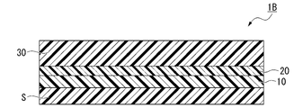
- FIG. 10 is a schematic cross-sectional view of an optical sheet 1B according to a third embodiment of the invention; It is a schematic cross section of the optical sheet 1C which concerns on 4th embodiment of this invention. It is a schematic cross section of optical sheet 1D which concerns on 5th embodiment of this invention.
- FIG. 11 is a schematic cross-sectional view of an optical sheet 1E according to a sixth embodiment of the invention; FIG.
- 11 is a schematic cross-sectional view of an optical sheet 1F according to a seventh embodiment of the invention.
- 4 is a graph showing light transmission profiles of transparent substrates. It is a spectrum of a light source used for evaluation of transmission characteristics. It is the spectrum of the light source used for evaluation of color reproducibility.
- FIGS. 1 to 7 are schematic cross-sectional views of optical sheets 1 and 1A to 1F according to first to seventh embodiments of the present invention, respectively.
- the upper side in FIGS. 1 to 7 corresponds to the observation side when observing the display image of the display device.
- FIG. 1 is a schematic cross-sectional view of an optical sheet 1 according to this embodiment.
- the optical sheet 1 includes a colored adhesive layer (first adhesive layer) 10 and an ultraviolet shielding layer 20 formed on the colored adhesive layer 10 . Both sides in the thickness direction of the optical sheet 1 are configured as sheets having adhesiveness. Both sides of the optical sheet 1 in the thickness direction are protected by a separator S or the like until use.
- the separator S a resin film, paper, or the like can be used.
- the optical sheet 1 can be used without peeling the separator S off.
- the direction in which the colored adhesive layer 10 and the ultraviolet shielding layer 20 are laminated is referred to as the thickness direction, and one side in the thickness direction (observation side when observing the displayed image of the display device) is the upper side. Okay, the other side is called the bottom side.
- the colored adhesive layer 10 contains an adhesive and a pigment.
- An adhesive is a resin that exhibits adhesiveness.
- the resin component of the pressure-sensitive adhesive is not particularly limited, and examples thereof include silicone-based pressure-sensitive adhesives, acrylic pressure-sensitive adhesives, and urethane-based pressure-sensitive adhesives. Dyes selectively absorb wavelength bands of visible light.
- the colored adhesive layer 10 has a structure in which a dye is contained in a base adhesive that exerts adhesiveness.
- the pigment includes at least one of the first to third coloring material groups shown below.
- the type of colorant to be included is not limited to one type, and two or more types of colorant may be included.
- the first coloring material has a maximum absorption wavelength within the range of 470 nm to 530 nm, and a half width (full width at half maximum) of the absorption spectrum of 15 nm to 45 nm.
- the second coloring material has a maximum absorption wavelength within the range of 560 nm to 620 nm, and a half width (full width at half maximum) of the absorption spectrum of 15 nm to 55 nm.
- the third colorant has a wavelength of 650 to 800 nm with the lowest transmittance in the wavelength range of 400 to 800 nm.
- the half width of the absorption spectrum refers to the full width at half maximum.
- the colored adhesive layer 10 has an absorption such that the transmittance of the maximum absorption wavelength in one of the absorption wavelength bands of the colorant is 1% or more and less than 50%.
- the first to third coloring materials to be contained in the colored adhesive layer 10 by using the coloring materials having the above-described absorption characteristics, among the visible light emitted by the display device, the wavelength range with relatively low emission intensity of visible light can be absorbed by the colored adhesive layer 10 .
- visible light in the wavelength range of 400 to 800 nm, visible light in the range of 470 nm to 530 nm, 560 nm to 620 nm, and 650 to 800 nm, respectively is colored adhesive. It can be absorbed into layer 10 .
- the wavelengths absorbed by the first, second, and third colorants are relatively It is a range that overlaps with the wavelength range where the emission intensity is low.
- the display device is not limited to the above organic EL display device, and other display devices may be used.
- a metal complex having a porphyrin structure, a pyrromethene structure, a phthalocyanine structure, or a squarylium structure in the molecule.
- the colored adhesive layer 10 may contain at least one of a radical scavenger, a singlet oxygen quencher and a peroxide decomposer.
- the colorant contained in the colored adhesive layer 10 is also degraded by light rays, heat, etc. accelerated under the influence of oxygen.
- a hindered amine light stabilizer can be used as a radical scavenger.
- a hindered amine light stabilizer having a molecular weight of 2,000 or more is particularly preferred because it provides a high effect of suppressing fading.
- the molecular weight of the radical scavenger is low, it is likely to volatilize, so few molecules remain in the colored adhesive layer 10, and it may be difficult to obtain a sufficient anti-fading effect.
- Examples of materials suitably used as radical scavengers include Chimassorb 2020FDL, Chimassorb 944FDL, Tinuvin 622 manufactured by BASF, and LA-63P manufactured by ADEKA.
- singlet oxygen quenchers include transition metal complexes, dyes, amines, phenols, and sulfides, and particularly preferred materials include dialkyl phosphate, dialkyldithiocarbanate, benzenedithiol, and the like. Transition metal complexes of dithiols can be exemplified, and nickel, copper or cobalt is preferably used as the central metal of these transition metal complexes.
- the peroxide decomposer decomposes the peroxide that is generated when the pigment is oxidatively deteriorated, stops the auto-oxidation cycle, and suppresses pigment deterioration (fading).
- Phosphorus-based antioxidants and sulfur-based antioxidants can be used as peroxide decomposers.
- Phosphorus antioxidants include, for example, 2,2′-methylenebis(4,6-di-t-butyl-1-phenyloxy)(2-ethylhexyloxy)phosphorus, 3,9-bis(2,6-di -tert-butyl-4-methylphenoxy)-2,4,8,10-tetraoxa-3,9-diphosphaspiro[5.5]undecane, and 6-[3-(3-t-butyl-4-hydroxy- 5-methylphenyl)propoxy]-2,4,8,10-tetra-t-butyldibenz[d,f][1,3,2]dioxaphosphepine and the like.
- sulfur-based antioxidants examples include 2,2-bis( ⁇ [3-(dodecylthio)propionyl]oxy ⁇ methyl)-1,3-propanediyl-bis[3-(dodecylthio)propionate], 2-mercaptobenz imidazole, dilauryl-3,3'-thiodipropionate, dimyristyl-3,3'-thiodipropionate, distearyl-3,3'-thiodipropionate, pentaerythrityl-tetrakis(3-laurylthiopropionate pionate), 2-mercaptobenzothiazole, and the like.
- the ultraviolet shielding layer 20 contains an ultraviolet absorber in order to suppress deterioration of the dye contained in the colored adhesive layer 10 . Thereby, the ultraviolet shielding layer 20 has an ultraviolet shielding rate of 85% or more.
- the UV shielding rate is a value measured according to JIS L 1925, and calculated by the following formula.
- Ultraviolet shielding rate (%) 100 - average transmittance of ultraviolet rays with a wavelength of 290 to 400 nm (%)
- the absorption wavelength range in the ultraviolet region of the ultraviolet absorbent contained in the ultraviolet shielding layer 20 is preferably in the range of 290 to 370 nm.
- ultraviolet absorbers include benzophenone-based, benzotriazole-based, triazine-based, oxalic acid anilide-based, and cyanoacrylate-based compounds.
- the ultraviolet absorber is blended in order to suppress deterioration of the dye contained in the colored adhesive layer 10 . For this reason, an ultraviolet absorber is used that absorbs light in the wavelength range that contributes to deterioration of the dye contained in the colored adhesive layer 10 in the ultraviolet region.
- the ultraviolet shielding layer 20 may further contain a resin exhibiting adhesiveness.
- the ultraviolet shielding layer 20 contains resin which exhibits adhesiveness, it is also called the "ultraviolet absorption adhesive layer 20" or the “second adhesive layer 20.”
- the ultraviolet-absorbing adhesive layer 20 there is no particular limitation on the resin component exhibiting adhesiveness, and the same resin as that for the colored adhesive layer 10 can be used.
- one of a colored adhesive layer 10 and an ultraviolet shielding layer (ultraviolet absorbing adhesive layer) 20 is formed on a base film made of resin or the like, and the other is formed thereon, and then the base film is peeled off. It can be manufactured by It may be used as the separator S as it is without peeling off the base film.
- the colored adhesive layer 10 and the ultraviolet shielding layer (ultraviolet absorbing adhesive layer) 20 can be formed, for example, by applying a coating liquid containing constituent materials of each layer and drying.
- the optical sheet 1 can attach the colored adhesive layer 10 or the ultraviolet shielding layer (ultraviolet absorbing adhesive layer) 20 to various objects by bonding, and can be provided with color correction capability.
- the object to which the optical sheet 1 is attached include various optically functional films such as antireflection films and antiglare films, display devices such as displays, and the like.
- the optical sheet 1 is attached so that external light including incident ultraviolet rays passes through the ultraviolet shielding layer (ultraviolet absorbing adhesive layer) 20 and then enters the colored adhesive layer 10 .
- wavelength components near the maximum absorption wavelength of the colorant contained therein are absorbed.
- the color purity of the display device can be improved.
- unlike a color filter it is not necessary to increase the color material concentration so much, so the color purity can be improved without excessively decreasing the luminance of the display device.
- the coloring material contained in the colored adhesive layer 10 has an excellent color correcting function, it may not have sufficient resistance to light rays, particularly ultraviolet rays. Therefore, when irradiated with ultraviolet rays, it deteriorates over time and becomes unable to absorb light in the vicinity of the maximum absorption wavelength.
- the ultraviolet shielding layer (ultraviolet absorbing adhesive layer) 20 has a high ultraviolet shielding rate. It does not pass through the absorbing adhesive layer) 20 and does not reach the colored adhesive layer 10 .
- ⁇ E*ab which is the chromaticity difference before and after the light resistance test (xenon lamp illuminance 60 W/cm 2 (300 to 400 nm), temperature 45° C., humidity 50% RH, irradiation for 120 hours), is calculated by the following formula ( 1): ⁇ E*ab ⁇ 5 Formula (1) can satisfy That is, it is possible to prevent deterioration of the coloring material contained in the colored adhesive layer 10, and to maintain the color correction function for a long time.
- ⁇ E*ab in Equation (1) is a chromaticity difference standardized by CIE (Commission international de l'eclairage).
- FIG. 2 is a schematic cross-sectional view showing the layer structure of the optical sheet 1A of this embodiment.
- the optical sheet 1A includes a transparent substrate 30 instead of the ultraviolet absorbing adhesive layer 20.
- the separator S is arranged only on the colored adhesive layer 10 side.
- the transparent substrate 30 has an ultraviolet shielding rate of 85% or more and functions as an ultraviolet shielding layer.
- the definition of the UV shielding rate is the same as that described for the UV shielding layer (ultraviolet absorbing adhesive layer) 20 .
- Materials for the transparent substrate 30 include polyolefins such as polyethylene and polypropylene; polyesters such as polyethylene terephthalate, polybutylene terephthalate and polyethylene naphthalate; polyacrylates such as polymethyl methacrylate; polyamides such as nylon 6 and nylon 66; Transparent resins such as arylate, polycarbonate, triacetylcellulose, polyacrylate, polyvinyl alcohol, polyvinyl chloride, cycloolefin copolymer, norbornene-containing resin, polyethersulfone, and polysulfone, and inorganic glass can be used.
- a film made of polyethylene terephthalate (PET), a film made of triacetyl cellulose (TAC), a film made of polymethyl methacrylate (PMMA), and a film made of polyester can be preferably used.
- the thickness of the transparent substrate 30 is not particularly limited, it is preferably 10 to 100 ⁇ m.
- FIG. 8 shows light transmission profiles of transparent substrates made of these materials.
- the UV shielding rate of the transparent base material is as follows, and any of them can be suitably used as the transparent base material 30 .
- the UV shielding rate of the transparent substrate may be based on the absorption characteristics of the resin itself, or may be the UV absorber exemplified for the UV shielding layer (UV absorbing adhesive layer) 20, and is not particularly limited.
- the transparent base material 30 suppresses deterioration of the coloring material contained in the colored adhesive layer 10 due to ultraviolet rays.
- a transparent adhesive layer may be provided on the side of the transparent substrate 30 on which the colored adhesive layer 10 is not provided (upper side of the transparent substrate 30). By doing so, the side on which the colored adhesive layer 10 is not provided can be bonded to the object, and versatility is enhanced.
- FIG. 3 is a schematic cross-sectional view showing the layer structure of the optical sheet 1B of this embodiment.
- the optical sheet 1B in the structure of the optical sheet 1, in the ultraviolet shielding layer (ultraviolet absorbing adhesive layer) 20, the surface opposite to the surface provided with the colored adhesive layer 10 (upper surface of the ultraviolet shielding layer 20) is provided with a transparent base material. 30.
- the transparent substrate 30 may contain the ultraviolet absorber exemplified for the ultraviolet shielding layer 20 .
- the separator S is arranged only on the surface (lower surface of the colored adhesive layer 10) of the colored adhesive layer 10 opposite to the surface on which the ultraviolet shielding layer (ultraviolet absorbing adhesive layer) 20 is provided.
- the transparent substrate 30 and the ultraviolet shielding layer (ultraviolet absorbing adhesive layer) 20 suppress deterioration of the coloring material contained in the colored adhesive layer 10 due to ultraviolet rays.
- the same effects as those of the optical sheet 1 according to the first embodiment and/or the optical sheet 1A according to the second embodiment, or greater effects can be obtained.
- a transparent adhesive layer may be provided on the side of the transparent substrate 30 on which the colored adhesive layer 10 is not provided (upper side of the transparent substrate 30). In this way, the side on which the colored adhesive layer 10 is not provided (upper side of the transparent base material 30) can be bonded to the object, and versatility is enhanced.
- FIG. 4 is a schematic cross-sectional view showing the layer structure of the optical sheet 1C of this embodiment.
- the optical sheet 1C has an oxygen barrier layer 40 on the surface of the transparent substrate 30 opposite to the surface on which the colored adhesive layer 10 is provided (the upper surface of the transparent substrate 30).
- the transparent base material 30 contains the absorption properties of the resin or the ultraviolet absorbing agent exemplified in the ultraviolet absorbing adhesive layer 20 and has an ultraviolet shielding ability
- the transparent base material 30 is an ultraviolet shielding layer as in the example shown in FIG. may be
- the oxygen barrier layer 40 is a transparent layer having optical transparency, and has an oxygen permeability of 10 cc/(m 2 ⁇ day ⁇ atm) or less, preferably 5 cc/(m 2 ⁇ day ⁇ atm) or less. It is more preferably 1 cc/(m 2 ⁇ day ⁇ atm) or less.
- the material for forming the oxygen barrier layer 40 preferably contains polyvinyl alcohol (PVA), ethylene-vinyl alcohol copolymer (EVOH), vinylidene chloride, siloxane resin, etc. Maxieve (registered trademark) manufactured by Mitsubishi Gas Chemical Company, Inc. , EVAL manufactured by Kuraray Co., Ltd., Saran Latex and Saran Resin manufactured by Asahi Kasei Corporation can be used.
- the thickness of the oxygen barrier layer 40 is not particularly limited, and may be a thickness that provides desired oxygen barrier properties.
- Inorganic particles may also be dispersed in the oxygen barrier layer 40 .
- Oxygen permeability can be further reduced by the inorganic particles, and oxidative deterioration (discoloration) of the colored adhesive layer 10 can be further suppressed.
- the size and content of the inorganic particles are not particularly limited, and may be appropriately set according to the thickness of the oxygen barrier layer 40 and the like.
- the size (maximum length) of the inorganic particles dispersed in the oxygen barrier layer 40 is preferably less than the thickness of the oxygen barrier layer 40, and the smaller the better.
- the size of the inorganic particles dispersed in the oxygen barrier layer 40 may be uniform or non-uniform. Specific examples of inorganic particles dispersed in the oxygen barrier layer 40 include silica particles, alumina particles, silver particles, copper particles, titanium particles, zirconia particles, and tin particles.
- the oxygen barrier layer 40 suppresses the deterioration of the coloring material contained in the colored adhesive layer 10 due to light rays, heat, etc., which are accelerated under the influence of oxygen in the outside air, and has a color correction function. Can last longer.
- the number and positions of the oxygen barrier layers 40 can be set appropriately.
- the oxygen barrier layer 40 may be laminated on the observer side above the colored adhesive layer 10 .
- an oxygen barrier layer 40 may be provided between the colored adhesive layer 10 and the transparent substrate 30.
- an oxygen barrier layer 40 is provided between the colored adhesive layer 10 and the ultraviolet absorbing adhesive layer 20 or between the ultraviolet absorbing adhesive layer 20 and the transparent substrate 30.
- oxygen barrier layer 40 oxygen contained in the outside air does not reach the colored adhesive layer 10 unless it permeates the oxygen barrier layer 40, as in the fourth embodiment.
- a transparent adhesive layer may be provided on the oxygen barrier layer 40 .
- FIG. 5 is a schematic cross-sectional view showing the layer structure of the optical sheet 1D of this embodiment.
- the optical sheet 1D includes a transparent base material 30, a colored adhesive layer 10 laminated on the first surface side of the transparent base material 30 (the lower surface side of the transparent base material 30), and the first surface on the transparent base material 30 opposite to the first surface. and an optical function layer 50 formed on the second surface of the side (the upper surface side of the transparent base material 30).
- the optical sheet 1D includes a hard coat layer 51 as an optical functional layer 50 and a low refractive index layer 52 formed on the hard coat layer 51 .
- the hard coat layer 51 preferably has a pencil hardness of H or higher with a load of 500 g on the surface.
- the hard coat layer 51 is a hard resin layer and enhances the scratch resistance of the optical sheet 1D. Moreover, the hard coat layer 51 may have a higher refractive index than the low refractive index layer 52 .
- the resin constituting the hard coat layer 51 is a resin that is polymerized and cured by irradiation with active energy rays such as ultraviolet rays and electron beams. Available.
- active energy rays such as ultraviolet rays and electron beams.
- active energy rays such as ultraviolet rays and electron beams. Available.
- (meth)acrylate is a generic term for both acrylate and methacrylate
- (meth)acryloyl is a generic term for both acryloyl and methacryloyl.
- Examples of monofunctional (meth)acrylate compounds include 2-hydroxyethyl (meth)acrylate, 2-hydroxypropyl (meth)acrylate, 2-hydroxybutyl (meth)acrylate, n-butyl (meth)acrylate, isobutyl ( meth)acrylate, t-butyl (meth)acrylate, glycidyl (meth)acrylate, acryloylmorpholine, N-vinylpyrrolidone, tetrahydrofurfuryl acrylate, cyclohexyl (meth)acrylate, 2-ethylhexyl (meth)acrylate, isobornyl (meth)acrylate ) acrylate, isodecyl (meth) acrylate, lauryl (meth) acrylate, tridecyl (meth) acrylate, cetyl (meth) acrylate, stearyl (meth) acrylate, benzyl (meth) acrylate,
- bifunctional (meth)acrylate compounds include ethylene glycol di(meth)acrylate, diethylene glycol di(meth)acrylate, butanediol di(meth)acrylate, hexanediol di(meth)acrylate, nonanediol di(meth) acrylates, ethoxylated hexanediol di(meth)acrylate, propoxylated hexanediol di(meth)acrylate, diethylene glycol di(meth)acrylate, polyethylene glycol di(meth)acrylate, tripropylene glycol di(meth)acrylate, polypropylene glycol di( Di(meth)acrylates such as meth)acrylate, neopentyl glycol di(meth)acrylate, ethoxylated neopentyl glycol di(meth)acrylate, tripropylene glycol di(meth)acrylate, and neopentylglycol
- tri- or higher functional (meth)acrylate compounds include trimethylolpropane tri(meth)acrylate, ethoxylated trimethylolpropane tri(meth)acrylate, propoxylated trimethylolpropane tri(meth)acrylate, and tris-2-hydroxyethyl.
- Tri(meth)acrylates such as isocyanurate tri(meth)acrylate, glycerin tri(meth)acrylate, pentaerythritol tri(meth)acrylate, dipentaerythritol tri(meth)acrylate, ditrimethylolpropane tri(meth)acrylate, etc.) Functional (meth)acrylate compounds, pentaerythritol tetra(meth)acrylate, ditrimethylolpropane tetra(meth)acrylate, dipentaerythritol tetra(meth)acrylate, dipentaerythritol penta(meth)acrylate, ditrimethylolpropane penta(meth)acrylate, ) acrylate, dipentaerythritol hexa (meth) acrylate, ditrimethylolpropane hexa (meth) acrylate trifunctional or higher polyfunctional (meth) acrylate compounds,
- Urethane (meth)acrylate can also be used as an active energy ray-curable resin.
- urethane (meth)acrylates include those obtained by reacting a product obtained by reacting a polyester polyol with an isocyanate monomer or a prepolymer with a (meth)acrylate monomer having a hydroxyl group. .
- urethane (meth)acrylates examples include pentaerythritol triacrylate hexamethylene diisocyanate urethane prepolymer, dipentaerythritol pentaacrylate hexamethylene diisocyanate urethane prepolymer, pentaerythritol triacrylate toluene diisocyanate urethane prepolymer, dipentaerythritol pentaacrylate toluene diisocyanate.
- Examples include urethane prepolymers, pentaerythritol triacrylate isophorone diisocyanate urethane prepolymers, and dipentaerythritol pentaacrylate isophorone diisocyanate urethane prepolymers.
- the resins described above may be used alone or in combination of two or more. Further, the above resin may be a monomer in the hard coat layer forming composition, or may be a partially polymerized oligomer.
- the hard coat layer 51 may contain the above-described UV absorber in order to suppress the deterioration of the pigment contained in the colored adhesive layer 10 .
- an ultraviolet absorber whose absorption wavelength range in the ultraviolet region is different from the absorption wavelength region in the ultraviolet region of the photopolymerization initiator, and to suppress curing inhibition when the ultraviolet absorber is contained.
- an acylphosphine oxide-based photopolymerization initiator can be preferably used.
- acylphosphine oxide-based photopolymerization initiators include diphenyl(2,4,6-trimethylbenzoyl)phosphine oxide and phenylbis(2,4,6-trimethylbenzoyl)phosphine oxide.
- composition for forming the hard coat layer 51 may contain metal oxide fine particles for the purpose of adjusting the refractive index and imparting hardness.
- Metal oxide fine particles include zirconium oxide, titanium oxide, niobium oxide, antimony trioxide, antimony pentoxide, tin oxide, indium oxide, indium tin oxide, and zinc oxide.
- the hard coat layer 51 can be easily formed by forming the hard coat layer 51 with an energy ray curable compound such as an ultraviolet curable resin.
- the hard coat layer 51 can be formed by applying a coating liquid containing an energy ray-curable compound, a polymerization initiator, and an ultraviolet absorber, and irradiating the corresponding energy ray.
- the low refractive index layer 52 is arranged on the side closest to the user (viewer) viewing the display when the optical sheet 1D is applied to the display device.
- the low refractive index layer 52 prevents strong reflection of external light and improves the visibility of the display device.
- the low refractive index layer 52 may be a layer made of an inorganic material or an inorganic compound.
- inorganic substances and inorganic compounds include fine particles such as LiF, MgF, 3NaF.AlF, AlF, Na 3 AlF 6 and silica fine particles.
- silica fine particles have voids inside the particles such as porous silica fine particles and hollow silica fine particles, it is effective in lowering the refractive index of the low refractive index layer.
- the composition for forming the low refractive index layer 52 may appropriately contain the photopolymerization initiator, solvent, and other additives described for the hard coat layer 51 .
- the refractive index of the low refractive index layer 52 should be lower than the refractive index of the transparent substrate 30, preferably 1.55 or less.
- the thickness of the low refractive index layer 52 is not particularly limited, but is preferably 40 nm to 1 ⁇ m.
- the low refractive index layer 52 may contain any one of silicon oxide, fluorine-containing silane compound, fluoroalkylsilazane, fluoroalkylsilane, fluorine-containing silicon-based compound, and perfluoropolyether group-containing silane coupling agent. These materials can impart water repellency and/or oil repellency to the low refractive index layer 52, so that antifouling properties can be enhanced.
- the low refractive index layer 52 may be formed by vapor deposition, sputtering, or the like, for example. Alternatively, it may be formed by applying a coating liquid containing the constituent material of the low refractive index layer 52 and drying it.
- the optical sheet 1 ⁇ /b>D according to this embodiment can exhibit the same effects as those of the above-described embodiments, and can exhibit optical functions based on the optical function layer 50 .
- FIG. 6 is a schematic cross-sectional view showing the layer structure of the optical sheet 1E of this embodiment.
- the optical sheet 1 ⁇ /b>E includes a colored adhesive layer 10 , an ultraviolet shielding layer 20 , a transparent substrate 30 and an optical functional layer 50 .
- the ultraviolet shielding layer 20 is formed on the first surface side of the transparent substrate 30 (the lower surface side of the transparent substrate 30).
- the optical function layer 50 is formed on the second surface of the transparent substrate 30 opposite to the first surface (the upper surface side of the transparent substrate 30).
- the optical sheet 1 ⁇ /b>E includes an antiglare layer 53 as the optical functional layer 50 .
- the optical sheet 1E includes the colored adhesive layer 10, the transparent substrate 30, and It is sufficient if the optical function layer 50 is provided.
- the anti-glare layer 53 is a layer that has minute unevenness on the surface and reduces reflection of outside light by scattering outside light with the unevenness.
- the antiglare layer 53 can be formed by applying and curing an antiglare layer forming composition containing an active energy ray-curable resin and, if necessary, organic fine particles and/or inorganic fine particles.
- the active energy ray-curable resin used in the composition for forming the antiglare layer the resin described for the hard coat layer 51 can be used.
- the film thickness of the antiglare layer 53 is not particularly limited, it is preferably 1 to 10 ⁇ m.
- the organic fine particles used in the composition for forming the antiglare layer are mainly materials that form fine irregularities on the surface of the antiglare layer 53 and provide the function of diffusing external light.
- translucent resin materials such as acrylic resins, polystyrene resins, styrene-(meth)acrylic acid ester copolymers, polyethylene resins, epoxy resins, silicone resins, polyvinylidene fluoride, and polyethylene fluoride resins are used. Resin particles can be used. In order to adjust the refractive index and the dispersibility of the resin particles, two or more kinds of resin particles having different materials (refractive indexes) may be mixed and used.
- the inorganic fine particles used in the composition for forming the antiglare layer are mainly materials for adjusting the sedimentation and aggregation of the organic fine particles in the antiglare layer 53 .
- silica fine particles, metal oxide fine particles, various mineral fine particles, and the like can be used.
- silica fine particles that can be used include colloidal silica and silica fine particles surface-modified with reactive functional groups such as (meth)acryloyl groups.
- metal oxide fine particles that can be used include alumina, zinc oxide, tin oxide, antimony oxide, indium oxide, titania, and zirconia.
- Mineral fine particles include, for example, mica, synthetic mica, vermiculite, montmorillonite, iron montmorillonite, bentonite, beidellite, saponite, hectorite, stevensite, nontronite, magadiite, islarite, kanemite, layered titanate, smectite, synthetic Smectite or the like can be used.
- Mineral fine particles may be either natural products or synthetic products (including substituted products and derivatives), and a mixture of both may be used.
- layered organoclays are more preferred.
- a layered organic clay is a swelling clay in which organic onium ions are introduced between layers.
- the organic onium ion is not limited as long as it can be organicized by utilizing the cation exchange property of the swelling clay.
- the synthetic smectite described above can be preferably used. Synthetic smectite has the function of increasing the viscosity of the coating liquid for forming the antiglare layer, suppressing the sedimentation of resin particles and inorganic fine particles, and adjusting the irregular shape of the surface of the optical function layer.
- the antiglare layer-forming composition may contain any one of silicon oxide, fluorine-containing silane compound, fluoroalkylsilazane, fluoroalkylsilane, fluorine-containing silicon-based compound, and perfluoropolyether group-containing silane coupling agent. good. Since these materials can impart water repellency and/or oil repellency to the antiglare layer 53, antifouling properties can be enhanced.
- the antiglare layer 53 is a layer in which a layer with a relatively high refractive index and a layer with a relatively low refractive index are laminated in order from the colored adhesive layer 10 side (lower side) by unevenly distributing the material. may be formed.
- the antiglare layer 53 in which the material is unevenly distributed for example, is coated with a composition containing a low refractive index material containing surface-modified silica fine particles or hollow silica fine particles and a high refractive index material, and the surfaces of both It can be formed by phase separation using the difference in free energy.
- the refractive index of the layer having a relatively high refractive index on the side of the transparent substrate 30 is set to 1.50 to 2.40, and the refractive index of the layer on the surface side of the optical sheet 1E is set to It is preferable that the refractive index of the layer having a relatively low refractive index is 1.20 to 1.55.
- the antiglare layer 53 can be formed, for example, by applying a coating liquid containing constituent materials of each layer and drying the coating liquid.
- the optical sheet 1 ⁇ /b>E according to this embodiment has the same effects as those of the above-described embodiments, and can exhibit optical functions based on the optical function layer 50 .
- FIG. 7 is a schematic cross-sectional view showing the layer structure of the optical sheet 1F of this embodiment.
- the optical sheet 1F includes a colored adhesive layer 10, an ultraviolet shielding layer 20, a transparent substrate 30, and an optical functional layer 50.
- the ultraviolet shielding layer 20 is formed on the first surface side of the transparent substrate 30 (the lower surface side of the transparent substrate 30).
- the optical function layer 50 is formed on the second surface of the transparent substrate 30 opposite to the first surface (the upper surface side of the transparent substrate 30).
- the optical sheet 1 ⁇ /b>E includes an antiglare layer 53 and a low refractive index layer 52 formed on the antiglare layer 53 as the optical functional layer 50 .
- the optical sheet 1F includes the colored adhesive layer 10, the transparent base material 30, and It is sufficient if the optical function layer 50 is provided.
- the optical sheet 1F is obtained by laminating the ultraviolet shielding layer 20 and the colored adhesive layer 10 or the colored adhesive layer 10 on the first surface side of the transparent base material 30 (the lower surface side of the transparent base material 30). It can be manufactured by sequentially forming the antiglare layer 53 and the low refractive index layer 52 on the second surface opposite to the one surface (the upper surface side of the transparent base material 30).
- the antiglare layer 53 and the low refractive index layer 52 can prevent reflection and strong reflection of external light, thereby improving the visibility of the display device.
- the optical function layer 50 is not limited to the configuration described above, and the optical function exhibited by changing the configuration also changes.
- an antireflection layer in which a plurality of low refractive index layers and high refractive index layers are combined is also an example of the optical function layer 50 in the present invention.
- the low refractive index layer may have the same structure as the low refractive index layer 52 described in the fifth embodiment.
- the high refractive index layer may be arranged below the low refractive index layer and have a higher refractive index than the low refractive index layer.
- An antireflection layer including a high refractive index layer and an antiglare layer is also an example of the optical function layer 50 in the present invention.
- the antiglare layer may have the same structure as the antiglare layer 53 described in the sixth embodiment.
- the high refractive index layer may be arranged below the antiglare layer 53 and have a higher refractive index than the antiglare layer 53 .
- the antireflection layer including the high refractive index layer and the antiglare layer may further have a low refractive index layer 52 .
- the optical function layer 50 may function as an ultraviolet shielding layer by imparting an ultraviolet shielding function (ultraviolet absorbing ability).
- the transparent substrate 30 does not have to have an ultraviolet shielding function.
- an ultraviolet absorber may be added to the hard coat layer 51 and the antiglare layer 53 .
- the hard coat layer 51 made of an ultraviolet curable resin contains an ultraviolet absorber, the absorption wavelength range of the polymerization initiator in the ultraviolet region is preferably different from that of the ultraviolet absorber in the ultraviolet region.
- optical sheet according to the present invention will be further described using examples and comparative examples.
- the present invention is not limited at all by the specific contents of each of the following examples.
- TAC Triacetyl cellulose film (TG60UL manufactured by Fuji Film Co., Ltd., substrate thickness 60 ⁇ m, UV shielding rate 92.9%)
- PMMA1 Polymethyl methacrylate film (W001U80 manufactured by Sumitomo Chemical Co., Ltd., substrate thickness 80 ⁇ m, UV shielding rate 93.4%)
- PMMA2 Polymethyl methacrylate film (W002N80 manufactured by Sumitomo Chemical Co., Ltd., substrate thickness 80 ⁇ m, UV shielding rate 13.9%)
- PET1 Polyethylene terephthalate film (SRF manufactured by Toyobo Co., Ltd., substrate thickness 80 ⁇ m, UV shielding rate 88.3%)
- PET2 Polyethylene terephthalate film (TOR20 manufactured by SKC, substrate thickness 40 ⁇ m, UV shielding rate 88.6%)
- compositions shown in Table 4 were prepared by using the materials of the hard coat layer forming composition used to form the hard coat layer below.
- DPHA dipentaerythritol hexaacrylate
- PETA penentaerythritol triacrylate
- the hard coat-forming composition shown in Table 4 was applied onto the transparent base material or oxygen barrier layer shown in Tables 1 to 3, dried in an oven at 80°C for 60 seconds, and then irradiated with an ultraviolet irradiation device.
- the coating film is cured by performing ultraviolet irradiation (light source H bulb, manufactured by Fusion UV Systems Japan Co., Ltd.) at a dose of 150 mJ / cm 2 , and the hard film shown in Tables 1 to 3 having a film thickness of 5.0 ⁇ m after curing.
- Coat layers 1 and 2 were formed. Since the hard coat layer 2 contains an ultraviolet absorber, it also functions as an ultraviolet shielding layer.
- composition for forming low refractive index layer (Composition for forming low refractive index layer) The following materials were used as the composition for forming a low refractive index layer.
- ⁇ Refractive index adjuster Porous silica fine particle dispersion (average particle diameter 75 nm, solid content 20%, solvent methyl isobutyl ketone) 8.5 parts by mass
- Antifouling agent Optool AR-110 (manufactured by Daikin Industries, Ltd., solid content 15%, solvent methyl isobutyl ketone) 5.6 parts by mass
- Active energy ray curable resin Pentaerythritol triacrylate 0.4 parts by mass Initiator: Omnirad 184 (manufactured by IGM Resins B.V.) 0.07 parts by mass
- Solvent Methyl isobutyl ketone 83.73 parts by mass
- the composition for forming a low refractive index layer having the above composition is applied, dried in an oven at 80 ° C. for 60 seconds, and then an ultraviolet irradiation device (Fusion UV Systems Japan Co., Ltd. , Light source H bulb) was used to cure the coating film by irradiating with ultraviolet rays at an irradiation dose of 200 mJ / cm 2 , and the low refractive index layers of Tables 1 to 3 having a film thickness after curing of 100 nm were formed. .
- an ultraviolet irradiation device Fusion UV Systems Japan Co., Ltd. , Light source H bulb
- composition for forming antiglare layer Composition for forming antiglare layer
- the following materials were used to prepare the compositions shown in Table 5.
- ⁇ Active energy ray-curable resin Light acrylate PE-3A (manufactured by Kyoeisha Chemical Co., Ltd., refractive index 1.52)
- ⁇ Photoinitiator Omnirad TPO (manufactured by IGM Resins B.V.)
- Organic fine particles Styrene-methyl methacrylate copolymer particles (refractive index 1.515, average particle size 2.0 ⁇ m)
- Inorganic fine particles 1 Synthetic smectite/inorganic fine particles 2: Alumina nanoparticles, average particle size 40 nm ⁇ Solvent toluene isopropyl alcohol
- Example 13 On the transparent substrate of Example 13 shown in Table 2, the composition for forming an antiglare layer shown in Table 5 was applied, dried in an oven at 80 ° C. for 60 seconds, and then irradiated with an ultraviolet irradiation device. The coating film was cured by irradiating with ultraviolet rays at 150 mJ/cm 2 (manufactured by Fusion UV Systems Japan, light source H bulb) to form the antiglare layer shown in Table 2 having a film thickness of 5.0 ⁇ m after curing.
- Adhesive resin 70 parts by mass of butyl acrylate (BA) / hydroxyethyl methacrylate (HEMA) copolymer solution dissolved in ethyl acetate
- Curing agent 0.037 parts by mass of isocyanate cross-linking agent
- Additive silane coupling Agent 0.048 parts by mass
- Solvent MEK (methyl ethyl ketone) 30 parts by mass
- First and second adhesive layer-forming compositions The compositions shown in Table 6 were prepared using the materials of the adhesive layer-forming composition used for forming the following first and second adhesive layers. The maximum absorption wavelength and half width of the coloring material were calculated from the spectral transmittance of the characteristic values in the adhesive layer.
- the composition for forming an adhesive layer obtained as described above is applied to a release substrate film so as to have a dry thickness of 25 ⁇ m, dried sufficiently, and then laminated with a release film, A sticky layer was obtained.
- the release film on one side of the obtained adhesive layer was peeled off, and the adhesive layer was attached to a non-alkali glass support (adherend) having a thickness of 0.7 mm.
- the release film on the other side of the adhesive layer was peeled off, and the substrates laminated with the functional layers shown in Tables 1 to 3 were laminated to obtain optical sheets 1 to 22.
- Each of the samples of Examples 1 to 14 and Comparative Examples 1 to 8 is constructed by bonding an optical sheet to an adherend.
- the adherend is not particularly limited as long as it is a material that does not interfere with the evaluation of the characteristics of the optical sheet, and may be other than alkali-free glass.
- Tables 7 and 8 show the results of evaluating the above items.
- the optical sheets of Examples 1 to 14 each include a first adhesive layer (colored adhesive layer) and a layer having ultraviolet absorption ability disposed above the first adhesive layer.
- the adhesive layer 8 which is the second adhesive layer
- the hard coat layer 2 contains an ultraviolet absorber.
- the base material has UV absorbability.
- the UV shielding rate of the layer arranged above the first adhesive layer is 85% or more. From the results in Tables 7 and 8, the optical sheet provided with the colored adhesive layer of the present invention significantly improved the light resistance by providing the upper layer with an ultraviolet shielding layer having an ultraviolet shielding rate of 85% or more.
- Display device characteristic evaluation In Examples 15 to 17 and Comparative Examples 9 to 12 below, display device characteristics of display devices 1 to 7 using the obtained optical sheets 6, 11, 12 and 19 to 22 were evaluated by simulation as follows. .
- the display devices 1 to 7 had a configuration in which an optical sheet was bonded to an organic EL display device (object).
- the spectral spectrum is as shown in FIG. 9 during white display, and the single spectrum as shown in FIG. Become.
- the transmittance of the obtained optical sheet was measured using an automatic spectrophotometer (U-4100, manufactured by Hitachi, Ltd.). A single spectral spectrum during white display of the EL display device was multiplied to calculate a spectral spectrum after transmission through the optical sheet.
- the Y value is calculated by multiplying the spectrum of the organic EL display device when white is displayed alone and the spectral spectrum after transmission of the optical sheet by the relative luminosity, and the spectrum of the organic EL display device when white is displayed alone. Efficiency was defined as the ratio when the Y value obtained from the above was 100, and was evaluated as an index of the transmission characteristics of the display device.
- the transmittance of the obtained optical sheet was measured using an automatic spectrophotometer (U-4100, manufactured by Hitachi, Ltd.). Red, green, and blue of the CIE (Commission International de l'eclairage) 1931 color system after transmission through the optical sheet are obtained by multiplying the single spectra during red display, green display, and blue display of the EL display device. Chromaticity (x, y) of each single color was calculated.
- CIE Commission International de l'eclairage
- Table 9 shows white display transmission characteristics and color reproducibility as evaluations of the characteristics of the display device.
- the display devices 1 to 3 (Examples 15 to 17) provided with the colored adhesive layer, which is the first adhesive layer in the present invention, exhibited an sRGB chromaticity inclusion rate of 99% or more, and the adhesive layer Color reproducibility was improved as compared with Comparative Example 9 containing no coloring material (not provided with a colored adhesive layer).
- Comparative Example 10 in which the first colorant and the second colorant have deep absorption in a plurality of wavelength bands, has low white display transmission characteristics. From this, when the first adhesive layer contains a plurality of types of colorants, the transmittance at the maximum absorption wavelength of only one of the maximum absorption wavelengths of each colorant is 1% or more and less than 50%.
- the optical sheet may include a first adhesive layer (colored adhesive layer) 10 and a layer having ultraviolet absorption ability disposed above the first adhesive layer.
- the layer having ultraviolet absorption ability may be the ultraviolet shielding layer 20 , the transparent base material 30 or the optical function layer 50 . It is preferable that the layer having an ultraviolet absorbing ability disposed above the first adhesive layer 10 has an ultraviolet shielding rate of 85% or more according to JIS L 1925.
- the optical sheet may further include an antistatic layer and an antifouling layer.
- the antireflection layer of the optical functional layer 50 of the optical sheet includes a high refractive index layer, an antiglare layer 53, and a low refractive index layer 52, and the high refractive index layer, the antiglare layer 53, or the low refractive index layer 52 is included. At least one of them may have antistatic properties, and at least one of the high refractive index layer, the antiglare layer 53 and the low refractive index layer 52 may have antifouling properties.
- an antistatic agent may be added to the high refractive index layer and the antiglare layer 53 to impart antistatic properties.
- the low refractive index layer 52 may contain a material having water repellency and/or oil repellency to impart antifouling properties to the low refractive index layer 52 .
- the high refractive index layer and the antiglare layer 53 may be provided with antifouling properties.
- At least one of the high refractive index layer, the antiglare layer 53 and the low refractive index layer 52 may be provided with both antistatic properties and antifouling properties. Thereby, a further function can be imparted to the optical function layer.
- the present invention can be used as an optical sheet used in display devices.
- Optical sheet 10 Colored adhesive layer (first adhesive layer) 20 UV shielding layer (ultraviolet absorbing adhesive layer, second adhesive layer) 30 transparent substrate (ultraviolet shielding layer) 40 oxygen barrier layer 50 optical function layer 51 hard coat layer 52 low refractive index layer 53 antiglare layer S separator
Landscapes
- Physics & Mathematics (AREA)
- Chemical & Material Sciences (AREA)
- General Physics & Mathematics (AREA)
- Optics & Photonics (AREA)
- Organic Chemistry (AREA)
- Health & Medical Sciences (AREA)
- Chemical Kinetics & Catalysis (AREA)
- Medicinal Chemistry (AREA)
- Polymers & Plastics (AREA)
- Toxicology (AREA)
- Engineering & Computer Science (AREA)
- Theoretical Computer Science (AREA)
- Inorganic Chemistry (AREA)
- Optical Filters (AREA)
- Electroluminescent Light Sources (AREA)
- Laminated Bodies (AREA)
- Devices For Indicating Variable Information By Combining Individual Elements (AREA)
- Optical Elements Other Than Lenses (AREA)
- Surface Treatment Of Optical Elements (AREA)
- Adhesives Or Adhesive Processes (AREA)
Priority Applications (4)
| Application Number | Priority Date | Filing Date | Title |
|---|---|---|---|
| JP2022576954A JP7468709B2 (ja) | 2021-01-19 | 2021-07-15 | 光学シート及び表示装置 |
| EP21921114.1A EP4283348A4 (en) | 2021-01-19 | 2021-07-15 | OPTICAL FILM AND DISPLAY DEVICE |
| KR1020237020844A KR20230129057A (ko) | 2021-01-19 | 2021-07-15 | 광학 시트 및 표시 장치 |
| CN202180091038.2A CN116710816A (zh) | 2021-01-19 | 2021-07-15 | 光学片材及显示装置 |
Applications Claiming Priority (2)
| Application Number | Priority Date | Filing Date | Title |
|---|---|---|---|
| JP2021-006750 | 2021-01-19 | ||
| JP2021006750 | 2021-01-19 |
Publications (1)
| Publication Number | Publication Date |
|---|---|
| WO2022158008A1 true WO2022158008A1 (ja) | 2022-07-28 |
Family
ID=82549642
Family Applications (1)
| Application Number | Title | Priority Date | Filing Date |
|---|---|---|---|
| PCT/JP2021/026647 Ceased WO2022158008A1 (ja) | 2021-01-19 | 2021-07-15 | 光学シート及び表示装置 |
Country Status (7)
| Country | Link |
|---|---|
| US (1) | US20230358931A1 (https=) |
| EP (1) | EP4283348A4 (https=) |
| JP (1) | JP7468709B2 (https=) |
| KR (1) | KR20230129057A (https=) |
| CN (1) | CN116710816A (https=) |
| TW (1) | TW202237405A (https=) |
| WO (1) | WO2022158008A1 (https=) |
Families Citing this family (2)
| Publication number | Priority date | Publication date | Assignee | Title |
|---|---|---|---|---|
| EP4283347A4 (en) * | 2021-01-19 | 2025-05-21 | Toppan Inc. | Optical film, display device, and composition for forming colored layer |
| JP7088353B1 (ja) * | 2021-03-12 | 2022-06-21 | 凸版印刷株式会社 | 粘着シート、光学シート及び表示装置 |
Citations (9)
| Publication number | Priority date | Publication date | Assignee | Title |
|---|---|---|---|---|
| JP2001147319A (ja) * | 1999-05-31 | 2001-05-29 | Fuji Photo Film Co Ltd | 光学フィルターおよび反射防止膜 |
| WO2006118277A1 (ja) * | 2005-04-28 | 2006-11-09 | Api Corporation | 近赤外線吸収色素含有粘着剤 |
| JP2009031733A (ja) * | 2007-07-02 | 2009-02-12 | Nitto Denko Corp | 色補正フィルター、画像表示装置および液晶表示装置 |
| JP2009115882A (ja) * | 2007-11-02 | 2009-05-28 | Toray Ind Inc | プラズマディスプレイパネル用フィルター |
| JP2010061066A (ja) * | 2008-09-08 | 2010-03-18 | Toray Ind Inc | ディスプレイ用フィルター |
| JP2011141356A (ja) * | 2010-01-06 | 2011-07-21 | Toppan Printing Co Ltd | 染料を含有する着色組成物、カラーフィルタ及びその製造方法、それを具備する液晶表示装置並びに有機el表示装置 |
| JP2018136361A (ja) * | 2017-02-20 | 2018-08-30 | 東洋インキScホールディングス株式会社 | カラーフィルタ用着色組成物、およびカラーフィルタ |
| JP2019056865A (ja) * | 2017-09-22 | 2019-04-11 | 株式会社巴川製紙所 | ディスプレイ用光学フィルタ及びこれを用いたディスプレイ |
| JP2021006750A (ja) | 2019-06-28 | 2021-01-21 | ダイニチ工業株式会社 | 加湿装置 |
Family Cites Families (9)
| Publication number | Priority date | Publication date | Assignee | Title |
|---|---|---|---|---|
| JPS5917659U (ja) | 1982-07-23 | 1984-02-02 | 株式会社日立製作所 | 光送信集積回路 |
| JP3708298B2 (ja) * | 1996-07-29 | 2005-10-19 | 三井化学株式会社 | 光記録媒体 |
| JPH11231301A (ja) * | 1998-02-10 | 1999-08-27 | Kureha Chem Ind Co Ltd | カラー画像表示装置 |
| JP2003315544A (ja) | 2002-04-23 | 2003-11-06 | Mitsubishi Chemicals Corp | 偏光フィルム及びこれを用いた液晶ディスプレイ装置 |
| JP5103849B2 (ja) | 2006-09-28 | 2012-12-19 | カシオ計算機株式会社 | 液晶表示装置 |
| JP2012247501A (ja) * | 2011-05-25 | 2012-12-13 | Asahi Glass Co Ltd | 光学フィルタおよび画像表示装置 |
| CN110799864A (zh) * | 2017-06-27 | 2020-02-14 | 住友化学株式会社 | 光学膜 |
| KR20190109988A (ko) * | 2018-03-19 | 2019-09-27 | 삼성에스디아이 주식회사 | 광학표시장치 및 이를 위한 광학 부재 |
| KR102939378B1 (ko) * | 2018-03-27 | 2026-03-13 | 세키스이가가쿠 고교가부시키가이샤 | 조광체 및 조광 창유리 |
-
2021
- 2021-07-15 JP JP2022576954A patent/JP7468709B2/ja active Active
- 2021-07-15 EP EP21921114.1A patent/EP4283348A4/en active Pending
- 2021-07-15 CN CN202180091038.2A patent/CN116710816A/zh active Pending
- 2021-07-15 WO PCT/JP2021/026647 patent/WO2022158008A1/ja not_active Ceased
- 2021-07-15 KR KR1020237020844A patent/KR20230129057A/ko active Pending
-
2022
- 2022-01-18 TW TW111101943A patent/TW202237405A/zh unknown
-
2023
- 2023-07-18 US US18/354,563 patent/US20230358931A1/en active Pending
Patent Citations (9)
| Publication number | Priority date | Publication date | Assignee | Title |
|---|---|---|---|---|
| JP2001147319A (ja) * | 1999-05-31 | 2001-05-29 | Fuji Photo Film Co Ltd | 光学フィルターおよび反射防止膜 |
| WO2006118277A1 (ja) * | 2005-04-28 | 2006-11-09 | Api Corporation | 近赤外線吸収色素含有粘着剤 |
| JP2009031733A (ja) * | 2007-07-02 | 2009-02-12 | Nitto Denko Corp | 色補正フィルター、画像表示装置および液晶表示装置 |
| JP2009115882A (ja) * | 2007-11-02 | 2009-05-28 | Toray Ind Inc | プラズマディスプレイパネル用フィルター |
| JP2010061066A (ja) * | 2008-09-08 | 2010-03-18 | Toray Ind Inc | ディスプレイ用フィルター |
| JP2011141356A (ja) * | 2010-01-06 | 2011-07-21 | Toppan Printing Co Ltd | 染料を含有する着色組成物、カラーフィルタ及びその製造方法、それを具備する液晶表示装置並びに有機el表示装置 |
| JP2018136361A (ja) * | 2017-02-20 | 2018-08-30 | 東洋インキScホールディングス株式会社 | カラーフィルタ用着色組成物、およびカラーフィルタ |
| JP2019056865A (ja) * | 2017-09-22 | 2019-04-11 | 株式会社巴川製紙所 | ディスプレイ用光学フィルタ及びこれを用いたディスプレイ |
| JP2021006750A (ja) | 2019-06-28 | 2021-01-21 | ダイニチ工業株式会社 | 加湿装置 |
Also Published As
| Publication number | Publication date |
|---|---|
| EP4283348A4 (en) | 2024-11-20 |
| CN116710816A (zh) | 2023-09-05 |
| TW202237405A (zh) | 2022-10-01 |
| JPWO2022158008A1 (https=) | 2022-07-28 |
| KR20230129057A (ko) | 2023-09-05 |
| JP7468709B2 (ja) | 2024-04-16 |
| EP4283348A1 (en) | 2023-11-29 |
| US20230358931A1 (en) | 2023-11-09 |
Similar Documents
| Publication | Publication Date | Title |
|---|---|---|
| JP7186249B2 (ja) | 光学フィルム、これを用いた表示装置、光学フィルムの製造に用いる着色層形成用組成物 | |
| US20230357603A1 (en) | Adhesive sheet, display device using the same, composition for forming adhesive layer used for production of adhesive film | |
| US20230358932A1 (en) | Optical film and display device | |
| JP7768045B2 (ja) | 着色層形成用組成物 | |
| JP7248057B2 (ja) | 光学フィルムおよび表示装置 | |
| US20230358931A1 (en) | Optical sheet and display device | |
| JP7468708B2 (ja) | 光学フィルム、及び表示装置 | |
| JP7724809B2 (ja) | 光学フィルム、これを用いた表示装置 | |
| JP7248058B2 (ja) | 光学フィルムおよび表示装置 | |
| TWI918830B (zh) | 光學薄膜及顯示裝置 |
Legal Events
| Date | Code | Title | Description |
|---|---|---|---|
| 121 | Ep: the epo has been informed by wipo that ep was designated in this application |
Ref document number: 21921114 Country of ref document: EP Kind code of ref document: A1 |
|
| ENP | Entry into the national phase |
Ref document number: 2022576954 Country of ref document: JP Kind code of ref document: A |
|
| WWE | Wipo information: entry into national phase |
Ref document number: 202180091038.2 Country of ref document: CN |
|
| NENP | Non-entry into the national phase |
Ref country code: DE |
|
| ENP | Entry into the national phase |
Ref document number: 2021921114 Country of ref document: EP Effective date: 20230821 |