WO2022153917A1 - 遺伝子検出用具及び遺伝子検出用キット - Google Patents
遺伝子検出用具及び遺伝子検出用キット Download PDFInfo
- Publication number
- WO2022153917A1 WO2022153917A1 PCT/JP2022/000225 JP2022000225W WO2022153917A1 WO 2022153917 A1 WO2022153917 A1 WO 2022153917A1 JP 2022000225 W JP2022000225 W JP 2022000225W WO 2022153917 A1 WO2022153917 A1 WO 2022153917A1
- Authority
- WO
- WIPO (PCT)
- Prior art keywords
- gene
- electrode
- layer
- metal layer
- gene detection
- Prior art date
- Legal status (The legal status is an assumption and is not a legal conclusion. Google has not performed a legal analysis and makes no representation as to the accuracy of the status listed.)
- Ceased
Links
Images



Classifications
-
- C—CHEMISTRY; METALLURGY
- C12—BIOCHEMISTRY; BEER; SPIRITS; WINE; VINEGAR; MICROBIOLOGY; ENZYMOLOGY; MUTATION OR GENETIC ENGINEERING
- C12M—APPARATUS FOR ENZYMOLOGY OR MICROBIOLOGY; APPARATUS FOR CULTURING MICROORGANISMS FOR PRODUCING BIOMASS, FOR GROWING CELLS OR FOR OBTAINING FERMENTATION OR METABOLIC PRODUCTS, i.e. BIOREACTORS OR FERMENTERS
- C12M1/00—Apparatus for enzymology or microbiology
-
- C—CHEMISTRY; METALLURGY
- C12—BIOCHEMISTRY; BEER; SPIRITS; WINE; VINEGAR; MICROBIOLOGY; ENZYMOLOGY; MUTATION OR GENETIC ENGINEERING
- C12Q—MEASURING OR TESTING PROCESSES INVOLVING ENZYMES, NUCLEIC ACIDS OR MICROORGANISMS; COMPOSITIONS OR TEST PAPERS THEREFOR; PROCESSES OF PREPARING SUCH COMPOSITIONS; CONDITION-RESPONSIVE CONTROL IN MICROBIOLOGICAL OR ENZYMOLOGICAL PROCESSES
- C12Q1/00—Measuring or testing processes involving enzymes, nucleic acids or microorganisms; Compositions therefor; Processes of preparing such compositions
- C12Q1/68—Measuring or testing processes involving enzymes, nucleic acids or microorganisms; Compositions therefor; Processes of preparing such compositions involving nucleic acids
- C12Q1/6844—Nucleic acid amplification reactions
-
- C—CHEMISTRY; METALLURGY
- C12—BIOCHEMISTRY; BEER; SPIRITS; WINE; VINEGAR; MICROBIOLOGY; ENZYMOLOGY; MUTATION OR GENETIC ENGINEERING
- C12Q—MEASURING OR TESTING PROCESSES INVOLVING ENZYMES, NUCLEIC ACIDS OR MICROORGANISMS; COMPOSITIONS OR TEST PAPERS THEREFOR; PROCESSES OF PREPARING SUCH COMPOSITIONS; CONDITION-RESPONSIVE CONTROL IN MICROBIOLOGICAL OR ENZYMOLOGICAL PROCESSES
- C12Q1/00—Measuring or testing processes involving enzymes, nucleic acids or microorganisms; Compositions therefor; Processes of preparing such compositions
- C12Q1/68—Measuring or testing processes involving enzymes, nucleic acids or microorganisms; Compositions therefor; Processes of preparing such compositions involving nucleic acids
- C12Q1/6844—Nucleic acid amplification reactions
- C12Q1/686—Polymerase chain reaction [PCR]
Definitions
- the present invention relates to a gene detection tool and a gene detection kit.
- the hybridization method has been widely used as a technique for detecting a gene having a specific base sequence, and an electrochemical detection method using an electrode type sensor is known as one of the techniques (1).
- an electrochemical detection method using an electrode type sensor is known as one of the techniques (1).
- Patent Document 1 Japanese Patent Document 1
- Patent Document 1 proposes that an amplification reaction and an electrochemical measurement of a test sample that may contain a gene to be detected are performed in the same amplification reaction tube provided with an electrode. An electrode is embedded in the wall surface of the amplification reaction tube so that an electrochemical measurement can be performed on the solution in the tube.
- a nucleic acid amplification buffer is injected into an amplification reaction tube, and a test sample is added. After closing and sealing the lid of the nucleic acid amplification buffer and the amplification reaction tube containing the test sample, the tube is set in the amplification device. Subsequently, the solution in the tube is heated by the amplification device to amplify the gene to be detected, and then the reduction current of the solution in the tube is measured.
- Patent Document 1 requires an operation of collecting a test sample in a sampling tool separate from the amplification reaction tube and an operation of adding the collected test sample to the amplification reaction tube, which is complicated. There was a problem.
- patient-derived samples for example, saliva samples and blood samples
- the amplification reaction tubes and sampling tools are basically disposable, so the sampling tools should be used. There is also a problem that the cost is increased by using the sample and the amount of waste generated by the inspection is increased.
- An object of the present invention is to provide a gene detection tool and a gene detection kit that can quickly collect and add a test sample by a simple operation and can further reduce the amount of waste.
- the gene detection tool includes a container body for accommodating a liquid for gene synthesis reaction, a container lid for sealing the container body, and a container lid provided on the container lid and inserted into the container body. It is provided with an electrode unit and a sampling unit, and the sampling unit is configured to be able to suck a test sample that may contain a gene to be detected.
- the sampling unit on the container lid, it is not necessary to use the sampling tool, so that the test sample can be quickly collected and added by a simple operation. At the same time, the amount of waste can be reduced.
- the sampling unit may be provided at the tip of the electrode unit.
- the operation of bringing the sampling part into contact with the test sample for sampling becomes easy, and when the container lid is attached to the container body, the gene synthesis reaction liquid contained in the container body is contained.
- the sampling part (test sample) can be reliably immersed in the sample.
- the saliva sample is easily and easily sucked and collected by the sampling part by bringing the sampling part provided at the tip of the electrode part into contact with saliva in the oral cavity of the patient. can.
- the gene detection tool can have a simple structure.
- the electrode portion includes a plurality of electrodes provided on an insulating base material, an insulating layer covering the electrodes, and a sensor portion in which a part of the plurality of electrodes is exposed.
- the sampling unit may be provided above the sensor unit.
- the electrode portion and the sampling portion are collected by providing the sampling portion on the sensor portion in which a part of the electrodes is exposed while preventing erroneous detection by covering the plurality of electrodes with an insulating layer.
- the part can be made compact and simple.
- the sampling portion is further formed by a recess of the insulating layer that opens to the outer surface of the electrode portion, and at least a part of the inner wall surface of the recess has hydrophilicity. You may do so.
- "at least a part of the inner wall surface is hydrophilic” means that the contact angle of the inner wall surface portion with respect to the test sample (aqueous liquid) is less than 90 degrees and it is easy to get wet.
- the hydrophilicity of the inner wall surface portion may be formed by either the chemical composition or the surface roughness of the inner wall surface portion.
- a simple structure can be realized by forming the sampling part with a part of the insulating layer, and the inner wall surface of the sampling part has hydrophilicity, so that the test sample can be obtained. It can be reliably sucked and collected in the sampling section.
- the electrode portion includes an action electrode and a reference electrode as the electrodes, or includes an action electrode and a reference electrode and a counter electrode, and the electrode is the insulating group.
- the upper portion includes a metal layer formed on the material, a carbon layer formed on the metal layer, and an upper adhesive layer formed between the upper surface of the metal layer and the carbon layer.
- the adhesive layer may be made of silicon.
- each electrode since each electrode has a metal layer, the electric resistance can be lowered and the measurement sensitivity can be improved. Further, by covering the metal layer with a carbon layer, oxidation-reduction of the metal layer can be prevented, and measurement sensitivity and reproducibility can be improved. Furthermore, by providing an upper adhesive layer made of silicon between the upper surface of the metal layer and the carbon layer, the adhesion between the metal layer and the carbon layer is improved, and silicon has a higher electrical resistivity than the metal. Since it is high, it is possible to suppress the generation of hydrogen on the upper surface of the metal layer during measurement, prevent the metal layer and the carbon layer from peeling off, and improve the measurement sensitivity and reproducibility.
- the gene detection kit of one embodiment of the present invention includes the gene detection tool of the above embodiment and the gene synthesis reaction solution.
- the gene synthesis reaction solution contains at least a primer capable of synthesizing a gene using the gene to be detected as a template.
- the gene detection tool of the above embodiment can quickly collect and add a test sample by a simple operation, and therefore, a gene detection operation in a medical institution, a testing institution, or the like. Becomes easier.
- the patient himself / herself can easily and surely collect and add his / her own sample sample (for example, saliva sample or blood sample) at home or the like, versatility and convenience are improved.
- the present invention can provide a gene detection tool and a gene detection kit that can quickly collect and add a test sample by a simple operation and can further reduce the amount of waste.
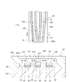
- FIG. 1 It is a schematic vertical sectional view which shows one Embodiment of a gene detection tool. It is an exploded side view which shows the same embodiment. It is a schematic diagram which shows the tip part of the electrode part of the same embodiment in an enlarged manner, (A) is a plan view which showed by omitting an insulating layer, (B) is a cross section corresponding to the BB position of (A). The figure, (C) is a cross-sectional view corresponding to the CC position of (A). It is a schematic diagram which shows the tip part of the electrode part of another embodiment in an enlarged manner, (A) is a plan view showing by omitting an insulating layer, and (B) corresponds to the DD position of (A). It is a sectional view. Each of (A) and (B) is a schematic cross-sectional view showing a tip portion of an electrode portion of still another embodiment.
- FIG. 1 is a schematic vertical sectional view showing the embodiment.
- FIG. 2 is an exploded side view showing the embodiment.
- FIG. 3 is an enlarged schematic view showing the tip of the electrode portion of the same embodiment,
- A) is a plan view,
- B) is a sectional view corresponding to the BB position of (A), and
- C Is a cross-sectional view corresponding to the CC position of (A).
- the gene detection tool 2 includes a container body 21 for accommodating the gene synthesis reaction liquid 10, a container lid 22 for sealing the container body 21, and an electrode portion provided on the container lid 22 and inserted into the container body 21. 23 and a sampling unit 24 are provided.
- the sampling unit 24 is configured to be able to suck a test sample that may contain a gene to be detected.
- the container body 21 has the form of a bottomed cylindrical member with one end closed and the other end open, and is a so-called tube.
- the container lid 22 is configured to be attached to the container body 21 so as to seal the opening 211 of the container body 21.
- the container lid 22 has a cylindrical lid cylinder portion 221 fitted into the opening 211 of the container main body 21, a lid top surface portion 222 that closes one end side of the lid cylinder portion 221 and an outer circumference of the lid cylinder portion 221. It has a substantially circular lid flange portion 223 that projects outward from the upper part of the surface.
- the electrode portion 23 is fixed to the container lid 22 so as to penetrate the lid top surface portion 222 of the container lid 22. As shown in FIG. 3, the electrode portion 23 includes a plurality of electrodes 232, 233, 234 provided on the insulating base material 231, an insulating layer 235 covering the electrodes 232, 233, 234, and electrodes 232, 233. , 234 is provided with a sensor unit 236 that exposes a part of 234.
- the insulating base material 231 has a substantially rectangular flat plate shape in a plan view.
- a working electrode 232, a counter electrode 233, and a reference electrode 234 are provided on the insulating base material 231 so as to be insulated from each other.
- the electrodes 232, 233, and 234 are formed of, for example, a gold thin film, and are provided from the vicinity of one end to the vicinity of the other end of the insulating base material 231 in the longitudinal direction.
- An insulating layer 235 that insulates the working electrode 232, the counter electrode 233, and the reference electrode 234 from each other is formed on the insulating base material 231.
- the insulating layer 235 has an adhesive layer (not shown) on the surface of the insulating base material 231 side. Then, the insulating layer 235 is attached to the insulating base material 231 so as to cover the electrodes 232, 233, 234, is embedded between the electrodes 232, 233, 234, and the side surfaces of the electrodes 232, 233, 234. Covering.
- the thickness of the insulating base material 231 is about 0.35 mm
- the thickness of the electrodes 232, 233, 234 is about 100 nm
- the thickness of the insulating layer 235 is about 0.1 mm.
- the thicknesses of the insulating base material 231, the electrodes 232, 233, 234 and the insulating layer 235 are schematically shown.
- a sampling portion 24 formed by a recess 235a of the insulating layer 235 that opens to the tip surface (outer surface) of the electrode portion 23 is provided on one end side of the electrode portion 23 .
- One end side of the working electrode 232, the counter electrode 233 and the reference electrode 234 is exposed in the sampling unit 24. That is, one end side of the working electrode 232, the counter electrode 233 and the reference electrode 234 is not covered with the insulating layer 235, and constitutes the sensor unit 236.
- the sampling unit 24 is provided at the tip of the electrode unit 23 and above the sensor unit 236.
- a silver chloride layer 237 is formed on the upper surface of the reference electrode 234 on one end side.
- At least a part of the inner wall surface of the recess 235a of the insulating layer 235 forming the sampling portion 24 has hydrophilicity.
- the inner wall surface of the top surface portion 241 of the sampling portion 24 has hydrophilicity, which facilitates suction collection of a test sample that may contain a gene to be detected.
- the surface of the insulating base material 231 exposed in the sampling unit 24 and the surface of the electrodes 232, 233, 234 may be hydrophilic.
- the container body 21 can be sealed by fitting the lid tube portion 221 of the container lid 22 into the opening 211 of the container body 21.
- the tip of the electrode unit 23 (the end where the sensor unit 236 and the sampling unit 24 are provided) is arranged near the bottom of the container body 21. ing. As a result, the sensor unit 236 and the sampling unit 24 are surely immersed in the gene synthesis reaction liquid 10 contained in the container body 21.
- the other end side of the electrode portion 23 is provided so as to project upward from the container lid 22.
- the other end side of the electrodes 232, 233, 234 (the end portion opposite to the sensor portion 236) is exposed, and the terminal portion 238 is formed.
- a connector 8 connected to the electrochemical measuring device is detachably attached to the terminal portion 238.
- the gene synthesis reaction liquid 10 is housed in the container body 21.
- the gene synthesis reaction liquid 10 may be pre-sealed in the container body 21 using a cap or film (not shown) separate from the container lid 22.
- the tester (for example, the patient himself / herself) picks up the container lid 22 and brings the tip of the electrode portion 23 into contact with a test sample that may contain a gene to be detected, and puts the sample collection section 24 on the sample. Collect the test sample by suction. For example, the patient himself / herself brings the tip of the electrode portion 23 into contact with saliva in his / her oral cavity, and collects a saliva sample as a test sample in the sampling portion 24.
- the inspector attaches the container lid 22 held in his hand to the container body 21, seals the container body 21, and immerses the tip of the electrode portion 23 in the gene synthesis reaction liquid 10.
- the test sample in the sampling unit 24 is diffused into the gene synthesis reaction solution 10. Further, the gene synthesis reaction liquid 10 enters the sampling unit 24, and the gene synthesis reaction liquid 10 comes into contact with the sensor unit 236. In this way, the tester can quickly and easily collect and add the test sample using the container lid 22 having the sampling unit 24.
- the entire gene detection tool 2, or at least the container body 21, is installed in an appropriate incubator (for example, a PCR device), while the connector 8 connected to the electrochemical measurement device is connected to the terminal 238 of the electrode 23. To connect.
- an appropriate incubator for example, a PCR device
- the incubator is operated to amplify the gene to be detected in the test sample, and the amplification of the gene to be detected is intermittently or continuously detected by the electrochemical measuring device.
- the detection process of the gene to be detected is performed in an incubator until the time predicted to be required for amplification of the gene to be detected (set amplification time) has elapsed. It is done after activating.
- the gene to be detected can be detected electrochemically while amplifying the gene to be detected.
- the test can be completed and the test time can be shortened. If the gene to be detected is not detected even after the set amplification time has elapsed from the start of the gene amplification process, it can be determined that the test sample does not contain the gene to be detected.
- the shape of the container body is not limited to the cylindrical shape shown in FIGS. 1 and 2, and may be any other shape such as a prismatic shape. Further, the gene detection tool of the present invention is not limited to the monochannel type in which the combination of the container body and the container lid is only one set, but is a multi-channel type including two or more sets of the container body and the container lid. May be good. In the case of the multi-channel type, the inspection can be performed under the same conditions.
- the dimensions of the gene detection tool of the present invention are not particularly limited.
- the total length of the gene detection tool 2 (on the bottom side of the container body 21).
- the total length from the end portion to the end portion of the electrode portion 23 on the terminal portion 238 side) can be about 20 to 60 mm, and the total length of the container body 21 can be about 10 to 50 mm.
- the inner diameter of the container body 21 can be, for example, about 3 to 10 mm.
- the gene detection tool of the present invention may be smaller or larger than the above dimensions.
- the material of the gene detection tool of the present invention is also not particularly limited, and can be molded from, for example, a plastic material (for example, polyolefin, particularly polyethylene, polyester, particularly polyethylene terephthalate, or polyacrylate, particularly polymethylmethacrylate).
- a plastic material for example, polyolefin, particularly polyethylene, polyester, particularly polyethylene terephthalate, or polyacrylate, particularly polymethylmethacrylate.
- a transparent material for example, polyolefin, particularly polyethylene, polyester, particularly polyethylene terephthalate, or polyacrylate, particularly polymethylmethacrylate.
- the material of the insulating base material 231 of the electrode portion 23 is not particularly limited, and for example, polystyrene (PI), glass, polyethylene terephthalate (PET), methacrylic resin (PMMA), polycarbonate (PC), polypropylene (PP), etc. Examples thereof include polyethylene (PE), polystyrene (PS), polyvinyl chloride (PVC), polyoxymethylene (POM), and ABS resin (ABS).
- the material of the insulating base material 231 is not limited to these, and may be ceramics, quartz, or the like. Further, the shape, thickness and size of the insulating base material 231 are not particularly limited.
- the gene to be detected to which the present invention can be applied is not particularly limited as long as it is a gene for which a primer for a gene synthesis reaction can be designed and a gene synthesis reaction can be carried out using the primer.
- the "gene” in the present specification includes both DNA and RNA.
- test sample to which the present invention can be applied is not particularly limited as long as it may contain a gene to be detected, and for example, a biological sample (for example, an animal (including human)).
- a biological sample for example, an animal (including human)
- Body fluids eg, saliva, blood, serum, plasma, spinal fluid, tears, sweat, urine, pus, or sputum
- excrement eg, feces
- organs, tissues, or animals and plants themselves or their dried bodies eg, an environment-derived sample (eg, river water, lake water, or seawater, or soil) can be mentioned.
- an environment-derived sample eg, river water, lake water, or seawater, or soil
- the present invention can be operated in a sealed state, it is particularly suitably applied to a dangerous test sample or a test sample in which a risk exists (for example, a test sample derived from a virus-infected patient). Can be done.
- the gene synthesis reaction solution 10 may contain an electrochemically active substance that can specifically bind to a gene.
- the electrochemically active substance specifically binds to a gene to generate a detectable electrochemical signal. That is, it does not bind to substances other than genes, but specifically binds to genes, and exhibits oxidative or reducing activity in electrochemical measurement.
- a specific voltage is applied to the sample solution in which the gene to which the electrochemically active substance is bound is present, a signal proportional to the amount of the gene-binding substance is obtained.
- the electrochemically active substance is not particularly limited as long as it can specifically bind to a gene and is an electrochemically active gene-binding substance, but for example, a double chain.
- An intercalating agent that can specifically bind to DNA and is electrochemically active is preferable.
- “specifically binds to double-stranded DNA” means that it does not bind to single-stranded DNA but binds to a gene.
- electrochemically active substance examples include bisbendiimide derivatives, ferrocene derivatives, quinone derivatives, indophenol derivatives, aclysine derivatives, flavin derivatives, viologen derivatives, ruthenium complexes, osmium complexes, cobalt complexes, platinum complexes, and copper complexes. , Actinomycin D or donomycin or derivatives thereof and the like.
- a test sample that may contain the gene to be detected and a gene synthesis reaction solution containing at least a primer capable of synthesizing the gene using the gene to be detected as a template are used.
- Perform a gene synthesis reaction is not particularly limited as long as it is a reaction capable of synthesizing a gene that binds to a gene-binding substance using the gene to be detected in the test sample as a template, but is not particularly limited, for example, gene amplification.
- a reaction, a replication reaction, a transcription reaction, or a reverse transcription reaction can be mentioned, and the gene amplification reaction is preferable.
- any known method for example, polymerase chain reaction (PCR), LAMP (Loop mediated isothermal amplification) method, ICAN (Isothermal and chimeric primer-initiated amplification of nucleic acids) method, TMA (Transcription mediated amplification) method ) Method, SDA (Strand displacement amplification) method, LCR (Ligase chain reaction) method, NASBA (Nucleic acid sequence-based amplification) method, or the like can be used.
- PCR polymerase chain reaction
- LAMP Loop mediated isothermal amplification
- ICAN Isothermal and chimeric primer-initiated amplification of nucleic acids
- TMA Transcription mediated amplification
- SDA String displacement amplification
- LCR Low cost of DNA mediated amplification
- NASBA Nucleic acid sequence-based amplification
- the reaction itself of the above gene synthesis reaction can be carried out in exactly the same way as a normal gene synthesis reaction.
- PCR when PCR is carried out as the above gene synthesis reaction, it can be carried out in the same manner as ordinary PCR.
- the gene to be detected is DNA
- a heat-resistant DNA polymerase for example, Taq polymerase
- an initial degeneration reaction for example, at 97 ° C. for 2 to 3 minutes
- DNA degeneration step
- annealing step of single-stranded DNA and primer 50-55 ° C for 30 seconds
- DNA synthesis step with heat-resistant DNA polymerase 70
- PCR can be performed by repeating the amplification cycle (eg, 15-45 times) consisting of ⁇ 75 ° C. for 1-2 minutes).
- RNA When the gene to be detected is RNA, it can be carried out by, for example, the reverse transcription PCR (RT-PCR) method. That is, after performing a reverse transcription reaction using reverse transcriptase and an oligo (dT) primer, an initial denaturation reaction and an initial denaturation reaction using a thermostable DNA polymerase (for example, Taq polymerase) as in the case of the above DNA. Subsequent amplification cycles can be repeated.
- RT-PCR reverse transcription PCR
- the gene to be detected is detected by electrochemically detecting the gene to be detected after the completion of the above (3) synthesis step and before the above (1) denaturation step.
- the test can be completed as a positive judgment even before the end of the specified number of amplification cycles.
- the electrochemical measuring device connected to the terminal portion 238 of the electrode portion 23 of the gene detection tool 2 is generated when a potential is applied to the solution in the container body 21 (for example, the gene synthesis reaction liquid 10 to which the test sample is added). By measuring the current value, the electrochemical response can be measured.
- LSV linear sweep voltammetry
- CA couloamperimetry
- CC coulochronometry
- CV cyclic voltammetry
- the detection in the test sample is based on the following principle.
- the presence or absence of the gene to be detected can be determined. That is, the electrochemically active substance can specifically bind to a gene and is electrochemically active. Therefore, the electrochemical response when the gene synthesis reaction solution 10 to which the test sample is added does not contain a gene or the amount of the gene is small, and the gene synthesis reaction solution 10 to which the test sample is added Comparing with the electrochemical response when a large amount of gene is contained, in the latter case, since the gene-binding substance binds to the gene, the electrochemical response of the latter is higher than that of the former. It is reduced, resulting in an electrochemically detectable difference.
- the electrochemical response is compared with the electrochemical response in a comparative test (for example, a test in which the gene synthesis reaction is not performed). Decreases. In this case, it can be determined that the gene to be detected is present in the test sample.
- the double-stranded DNA is inserted (that is, intercalation) between adjacent base pairs in the double-stranded DNA as a gene-binding substance.
- An insert that can specifically bind to can be used.
- the electrochemical response is higher than the electrochemical response in the comparative test. ,descend. In this case, it can be determined that the gene to be detected is present in the test sample.
- a threshold value may be set in advance for the current value generated when the potential is applied, and the presence or absence of the gene to be detected may be determined. In this case, since the comparative test does not have to be performed, the inspection operation can be simplified and the inspection cost can be reduced.
- the gene detection kit of the present invention contains a gene synthesis reaction solution in addition to the gene detection tool of the present invention described above.
- the gene synthesis reaction solution may contain an electrochemically active substance that can specifically bind to a gene.
- the gene synthesis reaction solution may be stored in a container separate from the gene detection tool, or may be enclosed in a container body.
- each of the working electrode 232, the counter electrode 233, and the reference electrode 234 has a metal layer 41 formed on the insulating base material 231 and a carbon layer 42 formed over the metal layer 41.
- a lower adhesive layer 43 formed between the insulating base material 231 and the metal layer 41, and an upper adhesive layer 44 formed between the upper surface of the metal layer 41 and the carbon layer 42 are provided.
- the lower adhesive layer 43 is a thin film that prevents the insulating base material 231 and the metal layer 41 from peeling off, and is formed of, for example, silicon.
- silicon any material having good adhesion to the insulating base material 231 and the metal layer 41 may be used, and in addition to silicon, for example, chromium, titanium, and tungsten can be used.
- the lower adhesive layer 43 may be formed of a surface-treated layer formed by subjecting the surface of the insulating base material 231 to a surface treatment for improving the adhesion with the metal layer 41.
- a surface treatment include plasma treatment, corona treatment, frame treatment, etching treatment, vapor treatment, ion beam treatment and the like.
- the metal layer 41 is formed of a material having a lower electrical resistivity than the carbon layer 42, and is formed on the lower adhesive layer 43.
- the metal layer 41 is for reducing the electrical resistance between one end and the other end of each of the working electrode 232, the counter electrode 233 and the reference electrode 234 (between the sensor unit 236 and the terminal unit 238).
- As the material of the metal layer 41 for example, silver, ruthenium, tantalum, titanium, copper, aluminum, platinum, niobium, zirconium, alloys of these elements, alloys of these elements and carbon, and the like can be used.
- the upper adhesive layer 44 is formed on the upper surface of the metal layer 41, is a thin film that prevents peeling between the upper surface of the metal layer 41 and the carbon layer 42, and is made of silicon.
- the carbon layer 42 is formed on the metal layer 41 via the upper adhesive layer 44.
- the carbon layer 42 is formed of, for example, amorphous carbon or diamond-like carbon (DLC).
- carbon Since carbon has the following characteristics, it is suitable for use of the carbon layer 42 that protects the metal layer 41. (1) Has excellent stability even in a vacuum of 3000 ° C (in air at 500 ° C), (2) is not easily attacked by chemicals, (3) does not allow gas or solution to permeate, (4) excellent hardness, Strong, (5) excellent electrical conductivity, (6) resistant to wetting of metal salts, etc., (7) good blood and tissue compatibility, (8) physical and chemical properties Is isotropic.
- the lower adhesive layer 43, the metal layer 41, the upper adhesive layer 44, and the carbon layer 42 are preferably manufactured by a vapor deposition method because the shape and film thickness of each layer can be controlled with high accuracy.
- a vapor deposition method a so-called physical vapor deposition method (PVD) such as a vacuum vapor deposition method, an ion plating method, or a sputtering method, or a so-called chemical vapor deposition method (CVD) can be used.
- PVD physical vapor deposition method
- CVD chemical vapor deposition method
- the manufacturing method of each layer is not limited to the vapor deposition method, and may be a printing method such as a screen printing method or an inkjet printing method.
- a second insulating layer 45 is formed on the insulating base material 231 so as to surround the contours of the lower adhesive layer 43, the metal layer 41, and the upper adhesive layer 44 in a plan view.
- the side surface of the metal layer 41 is covered with the second insulating layer 45.
- the side surface of the lower adhesive layer 43, the side surface of the upper adhesive layer 44, and the side surface of the carbon layer 42 are also covered with the second insulating layer 45.
- the lower surface of the second insulating layer 45 is in contact with the insulating base material 231.
- the lower adhesive layer 43, the metal layer 41, and the upper adhesive layer 44 are isolated from the surrounding atmosphere by being surrounded by the insulating base material 231 and the second insulating layer 45.
- the material of the second insulating layer 45 is not particularly limited, and examples thereof include a silicon oxide film (SiO2), a silicon nitride film (Si3N4), and aluminum oxide (Al2O3).
- the second insulating layer 45 is not limited to those made of these materials, and the side surfaces of the electrodes 232, 233 and 234 (at least the side surfaces of the metal layer 41) can be shielded from the surrounding atmosphere and do not allow moisture to pass through. It may be an insulator.
- the height position (thickness) of the upper surface of the second insulating layer 45 may be such that the second insulating layer 45 can cover at least the side surface of the metal layer 41.
- the height position of the upper surface of the second insulating layer 45 is about the same as the height position of the upper surface of the carbon layer 42.
- the electrodes 232, 233, and 234 have a metal layer 41 formed on the insulating insulating base material 231 and a carbon layer formed on the insulating base material 231 so as to cover the metal layer 41. It includes a 42 and a lower adhesive layer 43 formed between the insulating base material 231 and the metal layer 41. Since the electrodes 232, 233, and 234 have the metal layer 41, the electrical resistance can be lowered and the measurement sensitivity can be improved. Further, by covering the upper surface of the metal layer 41 with the carbon layer 42 and covering the side surface of the metal layer 41 with the second insulating layer 45, the redox of the metal layer 41 can be prevented, and the measurement sensitivity and reproducibility can be improved.
- the upper adhesive layer 44 made of silicon between the upper surface of the metal layer 41 and the carbon layer 42, the adhesion between the metal layer 41 and the carbon layer 42 is improved, and silicon is more electric than metal. Since the resistivity is high, it is possible to suppress the generation of hydrogen on the upper surface of the metal layer 41 during measurement. Further, since the side surface of the metal layer 41 is covered with the second insulating layer 45, moisture does not reach the side surface, and hydrogen can be prevented from being generated on the side surface of the metal layer 41. As a result, peeling of the insulating base material 231 and the metal layer 41 can be prevented, and the measurement sensitivity and reproducibility can be improved.
- the electrodes 232, 233, and 234 include the lower adhesive layer 43 formed between the insulating base material 231 and the metal layer 41, the insulating base material 231 and the metal layer 41 during the measurement It is possible to prevent a decrease in adhesion and improve measurement sensitivity and reproducibility.
- the metal layer 41, the carbon layer 42 and the adhesive layers 43 and 44 are formed by a vapor deposition method, and the metal layer 41, the carbon layer 42 and the adhesive layers 43 and 44 are formed in the same shape in a plan view. ing.
- the shape and film thickness of each layer 41, 42, 43, 44 can be controlled with high accuracy, and the entire electricity of each of the electrodes 232, 233, 234 can be controlled. The stability of resistance can be improved.
- the lower adhesive layer 43 is made of silicon. Since silicon has good adhesion to glass and metal, the adhesion between the metal layer 41 and the insulating base material 231 can be strengthened.
- the upper adhesive layer 44 is also made of silicon. Since silicon has good adhesion to metal and carbon, it is possible to strengthen the adhesion between the metal layer 41 and the carbon layer 42.
- the electrode portion 23 includes a working electrode 232, a reference electrode 234, and a counter electrode 233, it can be applied to a three-electrode electrochemical measurement.
- the electrical resistance of the working electrode 232, the reference electrode 234, and the counter electrode 233 can be lowered, the redox of the metal layer 41 can be prevented, and the metal layer 41 can be prevented from peeling off, so that the measurement sensitivity and reproducibility can be improved. ..
- the electrode portion 23 may be applicable to a two-electrode electrochemical measurement using a working electrode and a reference electrode. If both the working electrode and the reference electrode are composed of an electrode having a metal layer, a carbon layer and an adhesive layer, the electrical resistance of both the working electrode and the reference electrode can be lowered and the oxidation-reduction of the metal layer is prevented. It is possible to prevent the metal layer from peeling off, so that the measurement sensitivity and reproducibility can be improved.
- Silicon with a thickness of about 20 nm is used on a glass substrate with a thickness of about 2500 nm (2.5 ⁇ m) as an insulating base material 231 by a sputtering method using a metal mask having an opening pattern corresponding to the lower adhesive layer forming region.
- the layer was formed as a lower adhesive layer 43.
- the film thickness of the lower adhesive layer 43 made of silicon is not particularly limited.
- a silver layer having a thickness of about 150 nm is formed as a metal layer 41 on the lower adhesive layer 43 by a sputtering method. did.
- a silicon layer having a thickness of about 20 nm was formed as the upper adhesive layer 44 on the metal layer 41 by a sputtering method.
- the film thickness of the upper adhesive layer 44 made of silicon is not particularly limited.
- a carbon layer 42 having a thickness of about 1000 nm was formed on the upper adhesive layer 44 by a sputtering method using a metal mask having the same opening pattern as the opening pattern corresponding to the lower adhesive layer forming region.
- a working electrode 232, a counter electrode 233 and a reference electrode 234 having the lower adhesive layer 43, the metal layer 41, the upper adhesive layer 44 and the carbon layer 42 were formed.
- the lower adhesive layer 43, the metal layer 41, the upper adhesive layer 44, and the carbon layer 42 are used on the insulating base material 231 using the same metal mask. Was formed without being carried out of the chamber.
- the time required for film formation of the lower adhesive layer 43, the metal layer 41, the upper adhesive layer 44 and the carbon layer 42 can be shortened, and foreign matter can be prevented from adhering between the layers.
- the metal layer 41, the carbon layer 42, and the adhesive layers 43, 44 are formed in the same shape in a plan view.
- the line width of the electrodes 223, 233, 234 (dimensions in the width direction orthogonal to the longitudinal direction) is about 1.0 mm.
- the distance between the electrodes 223, 233, and 234 is about 0.5 mm.
- a metal mask having an opening pattern around the lower adhesive layer forming region is used, and the side surfaces (electrodes 232, 233, and carbon layers 42) of the lower adhesive layer 43, the metal layer 41, the upper adhesive layer 44, and the carbon layer 42 are used.
- a second insulating layer 45 having a thickness of about 1200 nm was formed on the insulating base material 231 so as to cover the side surface of 234). The second insulating layer 45 is formed so as to surround the electrodes 232, 233 and 234 and to be embedded between the electrodes 232, 233 and 234.
- the lower adhesive layer 43, the metal layer 41, the upper adhesive layer 44 and the carbon layer 42, and the second insulating layer 45 are formed by using a metal mask having an opening pattern.
- a metal mask having an opening pattern By forming the layers, patterning by an etching method or a lift-off method is not required after the film formation of each layer, and the manufacturing cost can be reduced.
- a silver layer having a thickness of about 100 nm was formed on the upper surface of the carbon layer 42 on one end side of the reference electrode 234 by a film forming method, and a silver chloride layer 237 was formed by chlorination treatment. In this way, the electrode portion 23 was manufactured.
- the silver-silver chloride layer 237 may be formed after the second insulating layer 45 is formed, or the silver-silver chloride layer 237 may be formed before the second insulating layer 45 is formed.
- the insulating layer 235 is attached on the insulating base material 231 so as to cover the electrodes 232, 233, 234 and the second insulating layer 45 to form the sensor unit 236 and the sampling unit 24.
- the film thickness of the metal layer 41 is not particularly limited, but is preferably 50 nm or more and 1000 nm or less. If the film thickness of the metal layer 41 is thinner than 50 nm, the electrodes 223, 233 and 234 have high resistance and the measurement sensitivity is lowered. Further, if the film thickness of the metal layer 41 is thicker than 1000 nm, when the metal layer 41 is formed by a vapor deposition method (for example, a sputtering method), the time required for forming the metal layer 41 becomes longer, and the production efficiency becomes higher. descend.
- a vapor deposition method for example, a sputtering method
- the manufacturing cost can be reduced by providing regions of a plurality of electrode portions 23 on one insulating base material 231 to form the plurality of electrode portions 23 at the same time, and then separating each electrode portion 23 into individual pieces. ..
- a surface treatment layer 46 formed by subjecting the surface of the insulating base material 231 to a surface treatment for improving adhesion is formed as a lower adhesive layer, and the surface treatment is performed.
- a metal layer 41 and a second insulating layer 45 may be formed on the layer 46.
- the insulating layer 235 has a lower insulating layer 235b in which a portion forming the sampling portion 24 is cut out and a lower insulating layer so as to cover the cutout portion of the lower insulating layer 235b. It may be formed by the upper insulating layer 235c formed on the 235b. Since the lower surface of the upper insulating layer 235c forming the top surface portion 241 of the sampling section 24 is hydrophilic, suction sampling of the test sample to the sampling section 24 can be reliably performed. In this way, the insulating layer 235 may be formed of a plurality of layers.
- the configuration of the insulating layer 235 shown in FIG. 5 (B) is also applicable to the insulating layer 235 of the electrode portion 23 shown in FIGS. 4 and 5 (A).
- the attachment structure of the container lid 22 to the container main body 21 may be a structure in which the container lid 22 is fitted to the outer periphery of the container main body 21, or may be a screw type connection structure.
- sampling unit 24 may be provided on the electrode unit 23 at a position different from that of the sensor unit 236, or may be provided on the container lid 22 at a position different from the electrode unit 23.
- the electrode portion 23 may have a configuration in which the working electrode 232 and the reference electrode 234 are provided as electrodes and the counter electrode 233 is not provided, and may be a configuration applicable to the two-electrode electrochemical measurement.
- 2 gene detection tool 10 gene synthesis reaction solution, 21 container body, 22 container lid, 23 electrode part, 24 sampling part, 41 metal layer, 42 carbon layer, 44 upper adhesive layer, 231 insulating base material, 232 action Electrode, 233 counter electrode, 234 reference electrode, 235 insulating layer, 235a recess, 236 sensor part
Landscapes
- Chemical & Material Sciences (AREA)
- Life Sciences & Earth Sciences (AREA)
- Organic Chemistry (AREA)
- Health & Medical Sciences (AREA)
- Engineering & Computer Science (AREA)
- Zoology (AREA)
- Wood Science & Technology (AREA)
- Bioinformatics & Cheminformatics (AREA)
- Proteomics, Peptides & Aminoacids (AREA)
- Biotechnology (AREA)
- General Engineering & Computer Science (AREA)
- Biochemistry (AREA)
- Genetics & Genomics (AREA)
- General Health & Medical Sciences (AREA)
- Microbiology (AREA)
- Chemical Kinetics & Catalysis (AREA)
- Biophysics (AREA)
- Physics & Mathematics (AREA)
- Analytical Chemistry (AREA)
- Immunology (AREA)
- Molecular Biology (AREA)
- Medicinal Chemistry (AREA)
- Biomedical Technology (AREA)
- Sustainable Development (AREA)
- Apparatus Associated With Microorganisms And Enzymes (AREA)
Priority Applications (2)
| Application Number | Priority Date | Filing Date | Title |
|---|---|---|---|
| JP2022575554A JP7756370B2 (ja) | 2021-01-14 | 2022-01-06 | 遺伝子検出用具及び遺伝子検出用キット |
| CN202280009510.8A CN116761897A (zh) | 2021-01-14 | 2022-01-06 | 基因检测用具和基因检测用试剂盒 |
Applications Claiming Priority (2)
| Application Number | Priority Date | Filing Date | Title |
|---|---|---|---|
| JP2021004242 | 2021-01-14 | ||
| JP2021-004242 | 2021-01-14 |
Publications (1)
| Publication Number | Publication Date |
|---|---|
| WO2022153917A1 true WO2022153917A1 (ja) | 2022-07-21 |
Family
ID=82447617
Family Applications (1)
| Application Number | Title | Priority Date | Filing Date |
|---|---|---|---|
| PCT/JP2022/000225 Ceased WO2022153917A1 (ja) | 2021-01-14 | 2022-01-06 | 遺伝子検出用具及び遺伝子検出用キット |
Country Status (3)
| Country | Link |
|---|---|
| JP (1) | JP7756370B2 (https=) |
| CN (1) | CN116761897A (https=) |
| WO (1) | WO2022153917A1 (https=) |
Citations (7)
| Publication number | Priority date | Publication date | Assignee | Title |
|---|---|---|---|---|
| WO2003089929A1 (en) * | 2002-04-22 | 2003-10-30 | Hokuto Scientific Industry, Co., Ltd. | Device, method, and kit for gene detection |
| WO2015025946A1 (ja) * | 2013-08-23 | 2015-02-26 | 京セラ株式会社 | センサ |
| JP2018060995A (ja) * | 2016-02-18 | 2018-04-12 | 株式会社半導体エネルギー研究所 | 半導体装置およびその作製方法、表示装置、並びに電子機器、 |
| JP2020031503A (ja) * | 2018-08-23 | 2020-02-27 | 株式会社半導体エネルギー研究所 | 半導体装置 |
| WO2021009845A1 (ja) * | 2019-07-16 | 2021-01-21 | 株式会社オプトラン | 電極及び電極チップ |
| WO2021192248A1 (ja) * | 2020-03-27 | 2021-09-30 | 子誠 朱 | 電極及び電極チップ |
| WO2021192247A1 (ja) * | 2020-03-27 | 2021-09-30 | 子誠 朱 | 電気化学分析チップ |
Family Cites Families (2)
| Publication number | Priority date | Publication date | Assignee | Title |
|---|---|---|---|---|
| TW200510724A (en) * | 2003-07-30 | 2005-03-16 | Riken | Kit for nucleic acid detection |
| JP6627564B2 (ja) * | 2016-02-25 | 2020-01-08 | 株式会社島津製作所 | 反応容器及びそれを用いた試薬キット |
-
2022
- 2022-01-06 JP JP2022575554A patent/JP7756370B2/ja active Active
- 2022-01-06 CN CN202280009510.8A patent/CN116761897A/zh active Pending
- 2022-01-06 WO PCT/JP2022/000225 patent/WO2022153917A1/ja not_active Ceased
Patent Citations (7)
| Publication number | Priority date | Publication date | Assignee | Title |
|---|---|---|---|---|
| WO2003089929A1 (en) * | 2002-04-22 | 2003-10-30 | Hokuto Scientific Industry, Co., Ltd. | Device, method, and kit for gene detection |
| WO2015025946A1 (ja) * | 2013-08-23 | 2015-02-26 | 京セラ株式会社 | センサ |
| JP2018060995A (ja) * | 2016-02-18 | 2018-04-12 | 株式会社半導体エネルギー研究所 | 半導体装置およびその作製方法、表示装置、並びに電子機器、 |
| JP2020031503A (ja) * | 2018-08-23 | 2020-02-27 | 株式会社半導体エネルギー研究所 | 半導体装置 |
| WO2021009845A1 (ja) * | 2019-07-16 | 2021-01-21 | 株式会社オプトラン | 電極及び電極チップ |
| WO2021192248A1 (ja) * | 2020-03-27 | 2021-09-30 | 子誠 朱 | 電極及び電極チップ |
| WO2021192247A1 (ja) * | 2020-03-27 | 2021-09-30 | 子誠 朱 | 電気化学分析チップ |
Non-Patent Citations (2)
| Title |
|---|
| NAOKI NAGATANI, KEIICHIRO YAMANAKA, MASATO SAITO, RITSUKO KOKETSU, TADAHIRO SASAKI, KAZUYOSHI IKUTA, TOSHIRO MIYAHARA, EIICHI TAMI: "Semi-real time electrochemical monitoring for influenza virus RNA by reverse transcription loop-mediated isothermal amplification using a USB powered portable potentiostat", THE ANALYST, vol. 136, no. 24, 1 January 2011 (2011-01-01), pages 5143, XP055181783, ISSN: 00032654, DOI: 10.1039/c1an15638a * |
| TAMIYA, EIICHI: "Development of Printable Biosensors", JOURNAL OF PRINTING SCIENCE AND TECHNOLOGY, vol. 51, no. 1, 1 January 2014 (2014-01-01), JP , pages 2 - 10, XP009538250, ISSN: 0914-3319, DOI: 10.11413/nig.51.002 * |
Also Published As
| Publication number | Publication date |
|---|---|
| JP7756370B2 (ja) | 2025-10-20 |
| CN116761897A (zh) | 2023-09-15 |
| JPWO2022153917A1 (https=) | 2022-07-21 |
Similar Documents
| Publication | Publication Date | Title |
|---|---|---|
| JP3642574B2 (ja) | 遺伝子検出用具、検出方法及び検出用キット | |
| EP3830572B1 (en) | Nanopore device and methods of detecting charged particles using same | |
| CN102103112B (zh) | 一种识别残留农药的光寻址分子印迹阵列传感器 | |
| BRPI0709971B1 (pt) | Método de fabrico de tiras de teste | |
| US20210247378A1 (en) | Nanopore device and methods of detecting and classifying charged particles using same | |
| JP7756370B2 (ja) | 遺伝子検出用具及び遺伝子検出用キット | |
| JP5193396B2 (ja) | ピロリン酸の測定方法およびsnpタイピング方法 | |
| CN115343343B (zh) | 一种用于冠状病毒核酸检测的微电极及其制备方法与应用 | |
| WO2010010211A2 (es) | Biosensor amperométrico desechable, método de fabricación del mismo y método de determinación de la presencia de analitos en alimentos | |
| CN101216451B (zh) | 一种dna生物传感器电极的制作方法及其应用 | |
| Franklin et al. | Iridium oxide reference electrodes for neurochemical sensing with MEMS microelectrode arrays | |
| JP4856017B2 (ja) | バイオセンサ | |
| JPWO2009130797A1 (ja) | Abo式血液型を判定するためのプローブセット | |
| Nair et al. | Microfluidic flexible device for real-time enzyme free uric acid detection | |
| BR102020012146B1 (pt) | Sensores eletroquímicos não enzimáticos para detecção de glicose em amostras de saliva | |
| BR102020012146A2 (pt) | Sensores eletroquímicos não enzimáticos para detecção de glicose em amostras de saliva | |
| CN109781821B (zh) | 一种血糖检测仪 | |
| Pucci | Microfluidic platform development for electrochemical biosensing of cancer biomarkers | |
| Petralla et al. | Miniaturized electrochemical cells for sensing applications: Silicon device containing three planar microelectrodes for electrochemical sensing | |
| Lenigk | Construction of electrochemical transducers with recessed microelectrode arrays for biomedical applications using CMOS processes | |
| Veselinovic | Nanoporous Gold Biosensors for Electrochemical Detection of Nucleic Acids | |
| JP4567490B2 (ja) | スーパーオキシドアニオンラジカルの測定方法 | |
| Lam et al. | Nanostructured Electrochemical Biosensors | |
| JP2006145342A (ja) | ポリヌクレオチドの分析方法 | |
| Tiwari et al. | Microfaradaic Electrochemical Biosensors for the Study of Anticancer Action of DNA Intercalating Drug: Epirubicin |
Legal Events
| Date | Code | Title | Description |
|---|---|---|---|
| 121 | Ep: the epo has been informed by wipo that ep was designated in this application |
Ref document number: 22739326 Country of ref document: EP Kind code of ref document: A1 |
|
| ENP | Entry into the national phase |
Ref document number: 2022575554 Country of ref document: JP Kind code of ref document: A |
|
| WWE | Wipo information: entry into national phase |
Ref document number: 202280009510.8 Country of ref document: CN |
|
| NENP | Non-entry into the national phase |
Ref country code: DE |
|
| 122 | Ep: pct application non-entry in european phase |
Ref document number: 22739326 Country of ref document: EP Kind code of ref document: A1 |