WO2022149557A1 - 酸化物スパッタリングターゲット、および、酸化物スパッタリングターゲットの製造方法 - Google Patents
酸化物スパッタリングターゲット、および、酸化物スパッタリングターゲットの製造方法 Download PDFInfo
- Publication number
- WO2022149557A1 WO2022149557A1 PCT/JP2021/048909 JP2021048909W WO2022149557A1 WO 2022149557 A1 WO2022149557 A1 WO 2022149557A1 JP 2021048909 W JP2021048909 W JP 2021048909W WO 2022149557 A1 WO2022149557 A1 WO 2022149557A1
- Authority
- WO
- WIPO (PCT)
- Prior art keywords
- oxide
- sputtering target
- oxide sputtering
- atomic
- range
- Prior art date
- Legal status (The legal status is an assumption and is not a legal conclusion. Google has not performed a legal analysis and makes no representation as to the accuracy of the status listed.)
- Ceased
Links
Images
Classifications
-
- C—CHEMISTRY; METALLURGY
- C04—CEMENTS; CONCRETE; ARTIFICIAL STONE; CERAMICS; REFRACTORIES
- C04B—LIME, MAGNESIA; SLAG; CEMENTS; COMPOSITIONS THEREOF, e.g. MORTARS, CONCRETE OR LIKE BUILDING MATERIALS; ARTIFICIAL STONE; CERAMICS; REFRACTORIES; TREATMENT OF NATURAL STONE
- C04B35/00—Shaped ceramic products characterised by their composition; Ceramics compositions; Processing powders of inorganic compounds preparatory to the manufacturing of ceramic products
- C04B35/01—Shaped ceramic products characterised by their composition; Ceramics compositions; Processing powders of inorganic compounds preparatory to the manufacturing of ceramic products based on oxide ceramics
- C04B35/453—Shaped ceramic products characterised by their composition; Ceramics compositions; Processing powders of inorganic compounds preparatory to the manufacturing of ceramic products based on oxide ceramics based on zinc, tin, or bismuth oxides or solid solutions thereof with other oxides, e.g. zincates, stannates or bismuthates
-
- C—CHEMISTRY; METALLURGY
- C23—COATING METALLIC MATERIAL; COATING MATERIAL WITH METALLIC MATERIAL; CHEMICAL SURFACE TREATMENT; DIFFUSION TREATMENT OF METALLIC MATERIAL; COATING BY VACUUM EVAPORATION, BY SPUTTERING, BY ION IMPLANTATION OR BY CHEMICAL VAPOUR DEPOSITION, IN GENERAL; INHIBITING CORROSION OF METALLIC MATERIAL OR INCRUSTATION IN GENERAL
- C23C—COATING METALLIC MATERIAL; COATING MATERIAL WITH METALLIC MATERIAL; SURFACE TREATMENT OF METALLIC MATERIAL BY DIFFUSION INTO THE SURFACE, BY CHEMICAL CONVERSION OR SUBSTITUTION; COATING BY VACUUM EVAPORATION, BY SPUTTERING, BY ION IMPLANTATION OR BY CHEMICAL VAPOUR DEPOSITION, IN GENERAL
- C23C14/00—Coating by vacuum evaporation, by sputtering or by ion implantation of the coating forming material
- C23C14/22—Coating by vacuum evaporation, by sputtering or by ion implantation of the coating forming material characterised by the process of coating
- C23C14/34—Sputtering
Definitions
- the present invention relates to an oxide sputtering target made of an oxide sintered body containing Zn as a main component as a metal component, and a method for manufacturing the oxide sputtering target.
- the present application claims priority based on Japanese Patent Application No. 2021-000440 filed in Japan on January 5, 2021, and the contents thereof are incorporated herein by reference.
- a protective film is formed in order to protect the recording layer and the light reflecting film.
- patterned wiring films and electrodes are widely used in electronic devices such as touch panels, solar cells, and organic EL displays, and these wiring films and electrodes have a structure in which a protective film is laminated on a metal film. It is said that.
- Patent Documents 1 and 2 oxide films such as ITO film and ZnO film having excellent visible light transmittance are used.
- the above-mentioned oxide film is formed by a sputtering method using an oxide sputtering target.
- Patent Documents 3 and 4 propose adding various elements to an oxide sputtering target in order to improve the characteristics of a ZnO film formed by a sputtering method.
- Patent Document 3 describes an oxide sputtering target in which Ti and one or more selected from Ga or Al are added to ZnO.
- the content of Ga or Al is 0.03 or less as the atomic number ratio of (Ga + Al) / (Zn + Ti + Ga + Al), and the content of Ti is 0.05 to 0 as the atomic number ratio of Ti / (Zn + Ti + Ga + Al). It is said to be .25.
- Patent Document 4 describes an oxide sputtering target in which Ti and Ga are added to ZnO.
- the Ti and Ga contents are in the range of Ti 1.1 at% or more or Ga 4.5 at% or more
- the Ga content y (at%) is the Ti content x (at%). It is in the range of the value represented by (-2.5x + 9.8) or less and the range of the value represented by the titanium content x (at%) (-0.5x + 1.1) or more.
- Japanese Patent Application Laid-Open No. 07-114841 A) Japanese Patent Application Laid-Open No. 2009-252576 (A) Japanese Patent Application Laid-Open No. 2009-298649 (A) Japanese Patent No. 4295811 (B)
- the characteristics of the formed oxide film vary depending on the initial / middle / final stage of the sputter film formation. In some cases, it was not possible to form an oxide film in a stable manner.
- the present invention has been made in view of the above-mentioned circumstances, and is an oxide sputtering target capable of stably forming a uniform oxide film with little variation in characteristics at the initial / middle / final stage of sputtering deposition.
- An object of the present invention is to provide a method for producing the oxide sputtering target.
- the oxide sputtering target of the present invention was made based on the above findings, and is composed of an oxide sintered body containing Zn as a main component as a metal component, and has a coefficient of variation of specific resistance value in the thickness direction. It is characterized by being 0.20 or less.
- the oxide sputtering target having the above configuration is composed of an oxide sintered body containing Zn as a main component as a metal component, and the fluctuation coefficient of the specific resistance value in the thickness direction is suppressed to 0.20 or less.
- the reduction state does not differ significantly between the surface layer, which is the sputtered surface of the target, and the inside, and even when sputtering progresses, it is possible to suppress variations in the film resistance of the deposited oxide film. , It becomes possible to stably form a uniform oxide film.
- Ga is 10.0 atomic% or more and 20.0 atomic% or less
- Ti is 0.5 atomic% or more and 5. It is preferably composed of an oxide containing 0 atomic% or less and the balance being Zn and an unavoidable impurity metal element.
- an oxide film can be stably formed by a normal sputtering method such as a DC (direct current) sputtering method. Further, when a laminated film with a metal is produced, a laminated film having excellent environmental resistance can be obtained.
- the oxide sputtering target of the present invention further, Zr, Hf, V, Nb, Ta, Cr, Mo, W, Mn, Fe, Co, Ni, B, Al, In, Si, Ge, Sn, A total of at least one or two or more additive elements selected from the element group consisting of elements of the Pb, Sb, Bi and lanthanoid series, 0.01 atomic% or more and 10.0 with the total metal component as 100 atomic%. It is preferably contained in the range of atomic% or less. In this case, it is possible to form an oxide film having further improved environmental resistance and a lower resistance value.
- the oxide has a composite oxide and the abundance ratio of the composite oxide is 15% or more.
- the oxide sintered body becomes dense, and cracks and cracks during sputtering can be more reliably suppressed.
- the method for producing an oxide sputtering target of the present invention is a method for producing an oxide sputtering target for producing the above-mentioned oxide sputtering target, which is a temporary firing step of tentatively firing a sintered raw material powder and a calcined raw material. It includes a crushing step of crushing the powder and a sintering step of sintering the crushed sintered raw material powder to obtain a sintered body, and the degree of vacuum in the preliminary firing step is within the range of 15 Pa or less. It is characterized in that the firing temperature is within the range of 600 ° C. or higher and 1000 ° C. or lower, and the holding time at the firing temperature is within the range of 2 hours or more and 6 hours or less.
- a calcination step of calcination raw material powder is provided, and the calcination conditions of the calcination step are defined as described above.
- the raw material powder can be reduced to a certain extent, and the local reduction reaction in the subsequent sintering step can be suppressed. As a result, the difference in the degree of reduction in the thickness direction becomes small, and the variation in the specific resistance value in the thickness direction can be suppressed.
- the degree of vacuum in the sintering step is within the range of 15 Pa or less
- the sintering temperature is within the range of 900 ° C. or higher and 1100 ° C. or lower
- the sintering temperature is high. It is preferable that the holding time is within the range of 2 hours or more and 6 hours or less.
- the sintering conditions in the sintering step are defined as described above, the composite oxide can be sufficiently produced and a dense oxide sintered body can be obtained.
- an oxide sputtering target capable of stably forming a uniform oxide film with little variation in characteristics at the initial / middle / final stage of sputter film formation, and a method for manufacturing the oxide sputtering target are provided. Can be provided.
- oxide sputtering target which is an embodiment of the present invention, and a method for manufacturing the oxide sputtering target will be described.
- the oxide sputtering target of the present embodiment is, for example, a protective film of an optical recording medium, a water vapor barrier film in various devices such as a liquid crystal display element, an organic EL element, and a solar cell, a touch panel, a solar cell, an organic EL display, and the like. It is used when forming an oxide film that serves as a wiring film and a protective film for electrodes in an electronic device.
- This oxide film is required to have excellent visible light transmittance, and in the present embodiment, it is an oxide film containing Zn as a main component as a metal component.
- the oxide sputtering target of the present embodiment is made of an oxide sintered body containing Zn as a main component as a metal component.
- the range of the Zn content ratio is preferably 60 atomic% or more and 90 atomic% or less.
- the coefficient of variation of the specific resistance value in the thickness direction is 0.20 or less, and the variation of the specific resistance value is suppressed to be small at least in the thickness direction of the sputtered surface.
- the coefficient of variation of the specific resistance value in the thickness direction is preferably 0.12 or less, and the coefficient of variation of the specific resistance value in the thickness direction is more preferably 0.10 or less.
- the lower limit of the coefficient of variation is not particularly limited, but may be 0.001.
- the thickness direction of the oxide sputtering target in the present embodiment means a direction substantially perpendicular to the main surface to be a sputtering surface, that is, a depth direction from the sputtering surface.
- the sputtered surface means a surface on which the sputtering particles are discharged when the sputtering process is performed.
- the oxide sputtering target has a flat plate shape, and the specific resistance value is set at a plurality of points in the thickness direction in one or more, preferably three or more regions in the main surface.
- the coefficient of variation is calculated by the following formula from the average value and standard deviation.
- Ga is 10.0 atomic% or more and 20.0 atomic% or less
- Ti is 0.5 atomic% or more and Ti is 0.5 atomic% or more, assuming that the total of the metal components is 100 atomic%. It may be composed of an oxide containing 5.0 atomic% or less and the balance being Zn and an unavoidable impurity metal element.
- additive elements selected from the element group consisting of elements of the lanthanoid series, 0.01 atomic% or more and 10.0 atoms with the total metal component as 100 atomic%. It may be contained in the range of% or less.
- the oxide sputtering target of the present embodiment may have either a single-phase oxide which is an oxide containing a single metal element or a composite oxide which is an oxide containing a plurality of metal elements.
- the abundance ratio of the composite oxide is preferably 15% or more. Further, the abundance ratio of the composite oxide is preferably 50% or less.
- the coefficient of variation of the specific resistance value in the thickness direction is preferably 0.12 or less.
- the composite oxide for example, when Ga and Ti are contained in addition to Zn, ZnGa 2 O 4 , ZnTIO 3 , Zn 2 TIO 4 , and the like can be mentioned.
- the abundance ratio of the composite oxide can be calculated from the intensity of the main peak of each phase (single phase oxide, composite oxide) by X-ray diffraction measurement (XRD).
- raw material powder such as zinc oxide powder is prepared.
- gallium oxide powder and titanium oxide powder are prepared in addition to zinc oxide powder, weighed so as to have a predetermined ratio, and mixed with a ball mill or the like. By mixing using an apparatus, a sintered raw material powder is obtained.
- Temporal firing step S02 Next, the sintered raw material powder is tentatively fired.
- the sintered raw material powder is inserted into the carbon crucible and temporarily fired in a vacuum atmosphere.
- the entire sintered raw material powder is slightly reduced.
- the sintered raw material powder may be temporarily fired in a reducing atmosphere such as CO gas or H2 gas.
- the degree of vacuum in the temporary firing step S02 is within the range of 15 Pa or less
- the firing temperature is within the range of 600 ° C. or higher and 1000 ° C. or lower
- the holding time at the firing temperature is within the range of 2 hours or more and 6 hours or less. It is said that.
- the crushed sintered raw material powder is filled in a molding die, pressed and heated to be sintered, and a sintered body is obtained.
- sintering is performed by a hot press device.
- the sintering temperature at this time is in the range of 900 ° C. or higher and 1100 ° C. or lower
- the holding time at the sintering temperature is in the range of 2 hours or more and 6 hours or less
- the pressurizing pressure is in the range of 10 MPa or higher and 35 MPa or lower. It is preferably inside.
- the atmosphere is preferably a vacuum atmosphere (15 Pa or less).
- a sufficient density can be obtained by setting the sintering temperature to 900 ° C. or higher.
- by setting the sintering temperature to 1100 ° C. or lower sublimation of zinc oxide can be suppressed, and composition deviation and occurrence of cracking of the sintered body can be suppressed.
- the oxide sputtering target of the present embodiment having the above configuration is composed of an oxide sintered body containing Zn as a main component as a metal component, and the coefficient of variation of the specific resistance value in the thickness direction is 0. Since it is suppressed to 20 or less, it is possible to suppress variations in the film resistivity of the oxide film formed even when sputtering progresses, and to stably form a uniform oxide film. Is possible.
- Ga is 10.0 atomic% or more and 20.0 atomic% or less
- Ti is 0.5 atomic% or more and 5.0, assuming that the total of the metal components is 100 atomic%.
- a stable oxide film is formed by a normal sputtering method such as a DC (DC) sputtering method. be able to. Further, in this case, an oxide film having excellent environmental resistance and alkali resistance can be formed.
- DC DC
- the environmental resistance of the oxide sputtering target is further improved, and an oxide film having a lower resistance value can be formed in the state after sputtering.
- the oxide sintered body becomes dense and cracks and cracks are more surely generated during sputtering. Can be suppressed.
- the method for producing an oxide sputtering target according to the present embodiment includes a tentative firing step S02 for tentatively firing the sintered raw material powder, in which the degree of vacuum in the tentative firing step S02 is within the range of 15 Pa or less and the firing temperature is 600. Since the holding time at the firing temperature is within the range of 2 hours or more and 6 hours or less within the range of ° C. or higher and 1000 ° C. or lower, the sintering raw material powder can be slightly reduced in advance, and the subsequent sintering can be performed. The local reduction reaction in the process can be suppressed. As a result, at least the difference in the degree of reduction in the thickness direction substantially perpendicular to the sputtered surface of the sintered body becomes small, and the variation in the specific resistance value in the thickness direction can be suppressed.
- the degree of vacuum in the sintering step S04 is within the range of 15 Pa or less
- the sintering temperature is within the range of 900 ° C. or higher and 1100 ° C. or lower
- the holding time at the sintering temperature is 2 hours or more and 6 hours.
- the present invention is not limited to this, and can be appropriately changed without departing from the technical idea of the invention.
- the present invention is not limited to this, and a cylindrical-shaped sputtering target may be used, or a sputtering target having another shape may be used. May be good.
- the thickness direction is the radial direction of the cylinder.
- a protective film for an optical recording medium a steam barrier film for various devices such as a liquid crystal display element, an organic EL element, and a solar cell, and a wiring film for an electronic device such as a touch panel, a solar cell, and an organic EL display.
- a steam barrier film for various devices such as a liquid crystal display element, an organic EL element, and a solar cell
- a wiring film for an electronic device such as a touch panel, a solar cell, and an organic EL display.
- raw material powder zinc oxide (ZnO) powder with an average particle size of 1 ⁇ m and a purity of 99.50 mass% or more, gallium oxide (Ga 2 O 3 ) powder with an average particle size of 2 ⁇ m and a purity of 99.99 mass% or more, and an average particle size of 15 ⁇ m. Titanium oxide (TiO 2 ) powder having a purity of 99.00 mass% or more was prepared. These raw material powders were weighed so as to have the composition shown in Table 1 and mixed uniformly with a ball mill device to obtain sintered raw material powders.
- the obtained sintered raw material powder was filled in a carbon crucible, and temporary firing (vacuum firing) was carried out under the conditions shown in Table 1. Then, the calcined raw material powder that had been calcined was crushed by a ball mill device. The sintered raw material powder after crushing was charged into a hot press device in a state of being filled in a carbon mold, and hot pressed under the conditions of atmosphere: vacuum, pressure 25 MPa, sintering temperature and holding time shown in Table 1. By grinding the obtained sintered body, Examples 1 to 14 and Comparative Examples 1 to 5 of the present invention having the same composition as the compounding composition of Table 1 having a diameter of 178 ⁇ 126 ⁇ 6 mm. Oxide sputtering target was prepared.
- ZnO (101) ICDD 01-080-0074 TiO 2 : (110) ICDD 01-076-1939 Ga 2 O 3 : (111) ICDD 01-087-1901 ZnGa 2 O 4 : (311) ICDD 01-086-0410 ZnTIO 3 : (104) ICDD 00-026-1500 Zn 2 TiO 4 : (311) ICDD 00-025-1164
- the specific resistance values were measured on the sputtered surface of the oxide sputtering targets of Examples 1 to 14 of the present invention and the surface ground by 1 mm from the sputtered surface, the surface grinded by 2 mm, and the surface grinded by 3 mm, respectively.
- the specific resistance value was measured by a four-probe method using a low resistivity meter (Loresta-GP) manufactured by Mitsubishi Chemical Corporation. The temperature at the time of measurement was 23 ⁇ 5 ° C., and the humidity was 50 ⁇ 20%.
- the mean value and standard deviation were obtained from the measurement results of four points, and the coefficient of variation of the specific resistance value in the thickness direction was calculated by acid.
- the film resistance of the oxide film formed at the initial stage of spatter film formation and the oxide film formed 2 hours after the start of spatter film formation was measured as follows.
- the film resistance was measured by a four-probe method using a low resistivity meter (Loresta-GP) manufactured by Mitsubishi Chemical Corporation.
- the firing temperature in the temporary firing step was 400 ° C., and the coefficient of variation of the specific resistance value of the oxide sputtering target was as large as 0.210.
- the film resistance changed significantly between the oxide film formed at the initial stage of sputter film formation and the oxide film formed 2 hours after the start of sputter film formation.
- the holding time at the firing temperature in the temporary firing step was set to 1 hour, and the coefficient of variation of the specific resistance value of the oxide sputtering target was as large as 0.220.
- the film resistance changed significantly between the oxide film formed at the initial stage of sputter film formation and the oxide film formed 2 hours after the start of sputter film formation.
- Comparative Examples 4 and 5 the temporary firing step was not carried out, and the coefficient of variation of the specific resistance value of the oxide sputtering target became as large as 0.240 and 0.310, respectively. As a result, the film resistance changed significantly between the oxide film formed at the initial stage of sputter film formation and the oxide film formed 2 hours after the start of sputter film formation. Further, in Comparative Examples 4 and 5, the contents of Ga and Ti were smaller than those in Comparative Example 3, and the composite oxide was not sufficiently produced. Therefore, cracks having a length of 2 mm or more were confirmed after the sputtering film formation.
- the firing temperature in the temporary firing step is within the range of 600 ° C. or higher and 1000 ° C. or lower, and the holding time at the firing temperature is within the range of 2 hours or more and 6 hours or less.
- the coefficient of variation of the specific resistance value of the oxide sputtering target was 0.20 or less. As a result, the amount of change in film resistance was suppressed between the oxide film formed at the initial stage of sputter film formation and the oxide film formed 2 hours after the start of sputter film formation.
- Example 11 of the present invention set at ° C. and Example 13 of the present invention in which the holding time at the firing temperature was 2 hours in the calcination step the composite oxide was not sufficiently formed and the length was 2 mm or more after the sputter film formation. Crack was confirmed.
- an oxide sputtering target capable of stably forming a uniform oxide film with little variation in characteristics at the initial / middle / final stage of sputtering deposition, and an oxide thereof. It was confirmed that it is possible to provide a method for manufacturing a sputtering target.
Landscapes
- Chemical & Material Sciences (AREA)
- Engineering & Computer Science (AREA)
- Materials Engineering (AREA)
- Organic Chemistry (AREA)
- Ceramic Engineering (AREA)
- Chemical Kinetics & Catalysis (AREA)
- Mechanical Engineering (AREA)
- Metallurgy (AREA)
- Manufacturing & Machinery (AREA)
- Structural Engineering (AREA)
- Physical Vapour Deposition (AREA)
- Compositions Of Oxide Ceramics (AREA)
Abstract
本発明の酸化物スパッタリングターゲットは、金属成分としてZnを主成分とする酸化物焼結体からなり、厚さ方向における比抵抗値の変動係数が0.20以下であることを特徴とする。本発明の酸化物スパッタリングターゲットの製造方法は、焼結原料粉を仮焼成する仮焼成工程と、焼成した焼結原料粉を解砕する解砕工程と、解砕した焼結原料粉を焼結して焼結体を得る焼結工程と、を備えており、前記仮焼成工程における真空度が15Pa以下の範囲内、焼成温度が600℃以上かつ1000℃以下の範囲内、焼成温度での保持時間が2時間以上かつ6時間以下の範囲内とされていることを特徴とする。
Description
本発明は、金属成分としてZnを主成分とする酸化物焼結体からなる酸化物スパッタリングターゲット、および、この酸化物スパッタリングターゲットの製造方法に関する。
本願は、2021年1月5日に、日本に出願された特願2021-000440号に基づき優先権を主張し、それらの内容をここに援用する。
本願は、2021年1月5日に、日本に出願された特願2021-000440号に基づき優先権を主張し、それらの内容をここに援用する。
従来、光ディスク等の光記録媒体においては、記録層や光反射膜を保護するために、保護膜が形成されている。
また、タッチパネルや太陽電池、有機ELディスプレイなどの電子デバイスにはパターニングされた配線膜や電極が広く使用されており、これら配線膜や電極においては、金属膜の上に保護膜が積層された構造とされている。
また、タッチパネルや太陽電池、有機ELディスプレイなどの電子デバイスにはパターニングされた配線膜や電極が広く使用されており、これら配線膜や電極においては、金属膜の上に保護膜が積層された構造とされている。
上述の保護膜として、例えば特許文献1,2に示すように、可視光の透過率に優れたITO膜やZnO膜などの酸化物膜が利用されている。
ここで、上述の酸化物膜は、酸化物スパッタリングターゲットを用いたスパッタ法によって成膜される。例えば、特許文献3,4には、スパッタ法により成膜されるZnO膜の特性を向上させるために、酸化物スパッタリングターゲットに各種元素を添加することが提案されている。
ここで、上述の酸化物膜は、酸化物スパッタリングターゲットを用いたスパッタ法によって成膜される。例えば、特許文献3,4には、スパッタ法により成膜されるZnO膜の特性を向上させるために、酸化物スパッタリングターゲットに各種元素を添加することが提案されている。
特許文献3には、ZnOに、Tiと、Ga又はAlから選ばれる1種以上を添加した酸化物スパッタリングターゲットが記載されている。この特許文献3では、Ga又はAlの含有量は、(Ga+Al)/(Zn+Ti+Ga+Al)原子数比として0.03以下、Tiの含有量は、Ti/(Zn+Ti+Ga+Al)原子数比として0.05~0.25とされている。
特許文献4には、ZnOに、TiとGaを添加した酸化物スパッタリングターゲットが記載されている。この特許文献4では、TiとGaの含有量は、Ti1.1at%以上又はGa4.5at%以上の範囲で、且つGaの含有量y(at%)が、Tiの含有量x(at%)で表される値(-2.5x+9.8)以下の範囲で且つチタンの含有量x(at%)で表される値(-0.5x+1.1)以上の範囲とされている。
ところで、金属成分としてZnを主成分とする酸化物焼結体からなる酸化物スパッタリングターゲットにおいては、スパッタ成膜の初期/中期/終期で、成膜された酸化物膜の特性にばらつきが生じ、安定して酸化物膜を成膜できないことがあった。
この発明は、前述した事情に鑑みてなされたものであって、スパッタ成膜の初期/中期/終期で特性のばらつきが少なく均一な酸化物膜を安定して成膜可能な酸化物スパッタリングターゲット、および、この酸化物スパッタリングターゲットの製造方法を提供することを目的とする。
上記課題を解決するために、本発明者らが鋭意検討した結果、以下のような知見を得た。金属成分としてZnを主成分とする酸化物焼結体からなる酸化物スパッタリングターゲットにおいては、焼結時に表層部分が局所的に還元されてしまい、表層と内部とで還元状態が異なることがわかった。そして、この還元状態の違いによって、該ターゲットにおける比抵抗値が変動することがわかった。
本発明の酸化物スパッタリングターゲットは、上述の知見に基づいてなされたものであって、金属成分としてZnを主成分とする酸化物焼結体からなり、厚さ方向における比抵抗値の変動係数が0.20以下であることを特徴としている。
上述の構成の酸化物スパッタリングターゲットによれば、金属成分としてZnを主成分とする酸化物焼結体からなり、厚さ方向における比抵抗値の変動係数が0.20以下に抑えられているので、該ターゲットのスパッタ面となる表層と内部とで還元状態がそれぞれ大きく異なっておらず、スパッタが進行した場合であっても、成膜した酸化物膜の膜抵抗にばらつきが生じることが抑えられ、均一な酸化物膜を安定して成膜することが可能となる。
ここで、本発明の酸化物スパッタリングターゲットにおいては、金属成分の合計を100原子%として、Gaが10.0原子%以上かつ20.0原子%以下、Tiが0.5原子%以上かつ5.0原子%以下、残部がZnおよび不可避不純物金属元素とされた割合で含有する酸化物からなることが好ましい。
この場合、上述の組成の酸化物で構成されているので、DC(直流)スパッタ法などの通常のスパッタ法により安定して酸化物膜を成膜することができる。また、金属との積層膜を作成した際に、耐環境性に優れた積層膜を得ることができる。
この場合、上述の組成の酸化物で構成されているので、DC(直流)スパッタ法などの通常のスパッタ法により安定して酸化物膜を成膜することができる。また、金属との積層膜を作成した際に、耐環境性に優れた積層膜を得ることができる。
また、本発明の酸化物スパッタリングターゲットにおいては、さらに、Zr、Hf、V、Nb、Ta、Cr、Mo、W、Mn、Fe、Co、Ni、B、Al、In、Si、Ge、Sn、Pb、Sb、Bi及びランタノイド系列の元素からなる元素群より選ばれる少なくとも1種または2種以上の添加元素を合計で、金属成分の合計を100原子%として0.01原子%以上かつ10.0原子%以下の範囲内で含有することが好ましい。
この場合、耐環境性がより向上し、抵抗値がより低減した酸化物膜を成膜することができる。
この場合、耐環境性がより向上し、抵抗値がより低減した酸化物膜を成膜することができる。
さらに、本発明の酸化物スパッタリングターゲットにおいては、複合酸化物を有し、複合酸化物の存在比率が15%以上であることが好ましい。
この場合、複合酸化物の存在比率が15%以上とされているので、酸化物焼結体が緻密となり、スパッタリング時の割れや亀裂の発生をより確実に抑制できる。
この場合、複合酸化物の存在比率が15%以上とされているので、酸化物焼結体が緻密となり、スパッタリング時の割れや亀裂の発生をより確実に抑制できる。
本発明の酸化物スパッタリングターゲットの製造方法は、上述の酸化物スパッタリングターゲットを製造する酸化物スパッタリングターゲットの製造方法であって、焼結原料粉を仮焼成する仮焼成工程と、焼成した焼結原料粉を解砕する解砕工程と、解砕した焼結原料粉を焼結して焼結体を得る焼結工程と、を備えており、前記仮焼成工程における真空度が15Pa以下の範囲内、焼成温度が600℃以上かつ1000℃以下の範囲内、焼成温度での保持時間が2時間以上かつ6時間以下の範囲内とされていることを特徴としている。
上述の構成の酸化物スパッタリングターゲットの製造方法によれば、焼結原料粉を仮焼成する仮焼成工程を備えており、仮焼成工程の焼成条件が上述のように規定されているので、焼結原料粉を一定程度還元処理することができ、その後の焼結工程における局所的な還元反応を抑制することができる。これにより、厚さ方向における還元度の差が小さくなり、厚さ方向における比抵抗値のばらつきを抑えることができる。
ここで、本発明の酸化物スパッタリングターゲットの製造方法においては、前記焼結工程における真空度が15Pa以下の範囲内、焼結温度が900℃以上かつ1100℃以下の範囲内、焼結温度での保持時間が2時間以上かつ6時間以下の範囲内とされていることが好ましい。
この場合、焼結工程における焼結条件が上述のように規定されているので、複合酸化物を十分に生成することができ、緻密な酸化物焼結体を得ることができる。
この場合、焼結工程における焼結条件が上述のように規定されているので、複合酸化物を十分に生成することができ、緻密な酸化物焼結体を得ることができる。
本発明によれば、スパッタ成膜の初期/中期/終期で特性のばらつきが少なく均一な酸化物膜を安定して成膜可能な酸化物スパッタリングターゲット、および、この酸化物スパッタリングターゲットの製造方法を提供することができる。
以下に、本発明の一実施形態である酸化物スパッタリングターゲット、および、酸化物スパッタリングターゲットの製造方法について説明する。
本実施形態である酸化物スパッタリングターゲットは、例えば、光記録媒体の保護膜、あるいは、液晶表示素子、有機EL素子、太陽電池等の各種デバイスにおける水蒸気バリア膜、タッチパネルや太陽電池、有機ELディスプレイなどの電子デバイスにおける配線膜および電極の保護膜となる酸化物膜を成膜する際に用いられるものである。
この酸化物膜は、可視光の透過率に優れていることが求められており、本実施形態では、金属成分としてZnを主成分とする酸化物膜とされている。
この酸化物膜は、可視光の透過率に優れていることが求められており、本実施形態では、金属成分としてZnを主成分とする酸化物膜とされている。
本実施形態である酸化物スパッタリングターゲットは、金属成分としてZnを主成分とする酸化物焼結体からなる。金属成分の合計を100原子%とした場合のZnの含有比率の範囲は、60原子%以上かつ90原子%以下であることが好ましい。
そして、本実施形態である酸化物スパッタリングターゲットにおいては、厚さ方向における比抵抗値の変動係数が0.20以下とされており、少なくともスパッタ面の厚さ方向において比抵抗値のばらつきが小さく抑えられている。また、厚さ方向における比抵抗値の変動係数は0.12以下が好ましく、更には厚さ方向における比抵抗値の変動係数は0.10以下がより好ましい。変動係数の下限値については、特に限定されないが、0.001としてもよい。
本実施形態における酸化物スパッタリングターゲットの厚さ方向は、スパッタ面となる主面に略垂直な方向、すなわち、スパッタ面からの深さ方向を意味している。スパッタ面は、スパッタリング処理を行う際に、スパッタリング粒子が放出される面を意味している。
なお、本実施形態では、酸化物スパッタリングターゲットは、平板形状をなしており、主面内の一つ以上、好ましくは三つ以上の領域において、その厚さ方向の複数の点で比抵抗値を測定し、その平均値と標準偏差とから、下記の式によって変動係数が算出される。比抵抗値を複数領域で測定する場合、測定した全領域で算出される変動係数の平均を、酸化物スパッタリングターゲットの変動係数とする。
(変動係数)=(標準偏差)/(平均値)
そして、本実施形態である酸化物スパッタリングターゲットにおいては、厚さ方向における比抵抗値の変動係数が0.20以下とされており、少なくともスパッタ面の厚さ方向において比抵抗値のばらつきが小さく抑えられている。また、厚さ方向における比抵抗値の変動係数は0.12以下が好ましく、更には厚さ方向における比抵抗値の変動係数は0.10以下がより好ましい。変動係数の下限値については、特に限定されないが、0.001としてもよい。
本実施形態における酸化物スパッタリングターゲットの厚さ方向は、スパッタ面となる主面に略垂直な方向、すなわち、スパッタ面からの深さ方向を意味している。スパッタ面は、スパッタリング処理を行う際に、スパッタリング粒子が放出される面を意味している。
なお、本実施形態では、酸化物スパッタリングターゲットは、平板形状をなしており、主面内の一つ以上、好ましくは三つ以上の領域において、その厚さ方向の複数の点で比抵抗値を測定し、その平均値と標準偏差とから、下記の式によって変動係数が算出される。比抵抗値を複数領域で測定する場合、測定した全領域で算出される変動係数の平均を、酸化物スパッタリングターゲットの変動係数とする。
(変動係数)=(標準偏差)/(平均値)
ここで、本実施形態である酸化物スパッタリングターゲットにおいては、金属成分の合計を100原子%として、Gaが10.0原子%以上かつ20.0原子%以下、Tiが0.5原子%以上かつ5.0原子%以下、残部がZnおよび不可避不純物金属元素とされた割合で含有する酸化物で構成されていてもよい。
また、Ga,Ti,Znに加えて、さらに、Zr、Hf、V、Nb、Ta、Cr、Mo、W、Mn、Fe、Co、Ni、B、Al、In、Si、Ge、Sn、Pb、Sb、Bi及びランタノイド系列の元素からなる元素群より選ばれる少なくとも1種または2種以上の添加元素を合計で、金属成分の合計を100原子%として0.01原子%以上かつ10.0原子%以下の範囲内で含有していてもよい。
また、Ga,Ti,Znに加えて、さらに、Zr、Hf、V、Nb、Ta、Cr、Mo、W、Mn、Fe、Co、Ni、B、Al、In、Si、Ge、Sn、Pb、Sb、Bi及びランタノイド系列の元素からなる元素群より選ばれる少なくとも1種または2種以上の添加元素を合計で、金属成分の合計を100原子%として0.01原子%以上かつ10.0原子%以下の範囲内で含有していてもよい。
また、本実施形態である酸化物スパッタリングターゲットは、単数の金属元素を含む酸化物である単相酸化物、複数の金属元素を含む酸化物である複合酸化物のいずれを有してもよい。酸化物スパッタリングターゲットを構成する酸化物のうち、複合酸化物の存在比率が15%以上であることが好ましい。また、複合酸化物の存在比率は50%以下であることが好ましい。なお、酸化物スパッタリングターゲットにおける複合酸化物の存在比率が15%以上である場合、厚さ方向における比抵抗値の変動係数は0.12以下が好ましい。
ここで、複合酸化物としては、例えば、Znの他にGa、Tiを含有する場合には、ZnGa2O4,ZnTiO3,Zn2TiO4等が挙げられる。
なお、複合酸化物の存在比率は、X線回折測定(XRD)による各相(単相酸化物、複合酸化物)のメインピークの強度から算出することができる。例えば、Znの他にGa、Tiを含有する場合には、ZnO相,Ga2O3相,TiO2相のピーク強度の合計Aと、上述の複合酸化物(ZnGa2O4,ZnTiO3,Zn2TiO4等)のピーク強度の合計Bとから、複合酸化物の存在比率は、以下の式で算出される。
複合酸化物の存在比率(%)=B/(A+B)×100
ここで、複合酸化物としては、例えば、Znの他にGa、Tiを含有する場合には、ZnGa2O4,ZnTiO3,Zn2TiO4等が挙げられる。
なお、複合酸化物の存在比率は、X線回折測定(XRD)による各相(単相酸化物、複合酸化物)のメインピークの強度から算出することができる。例えば、Znの他にGa、Tiを含有する場合には、ZnO相,Ga2O3相,TiO2相のピーク強度の合計Aと、上述の複合酸化物(ZnGa2O4,ZnTiO3,Zn2TiO4等)のピーク強度の合計Bとから、複合酸化物の存在比率は、以下の式で算出される。
複合酸化物の存在比率(%)=B/(A+B)×100
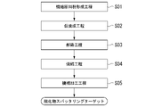
次に、本実施形態である酸化物スパッタリングターゲットの製造方法について、図1のフロー図を参照して説明する。
(焼結原料粉形成工程S01)
まず、酸化亜鉛粉等の原料粉を準備する。例えば、Znの他にGa、Tiを含有する場合には、酸化亜鉛粉の他に酸化ガリウム粉と酸化チタン粉を準備し、これらを所定の割合となるように秤量して、ボールミル等の混合装置を用いて混合することにより、焼結原料粉を得る。
まず、酸化亜鉛粉等の原料粉を準備する。例えば、Znの他にGa、Tiを含有する場合には、酸化亜鉛粉の他に酸化ガリウム粉と酸化チタン粉を準備し、これらを所定の割合となるように秤量して、ボールミル等の混合装置を用いて混合することにより、焼結原料粉を得る。
(仮焼成工程S02)
次に、焼結原料粉を仮焼成する。本実施形態では、カーボン坩堝内に焼結原料粉を挿入し、真空雰囲気で仮焼成する。この仮焼成工程S02により、焼結原料粉の全体を微還元処理しておく。なお、仮焼成工程S02においては、COガス、H2ガス等の還元雰囲気下で焼結原料粉を仮焼成してもよい。
ここで、仮焼成工程S02における真空度は15Pa以下の範囲内とされ、焼成温度は600℃以上かつ1000℃以下の範囲内、焼成温度での保持時間が2時間以上かつ6時間以下の範囲内とされている。
次に、焼結原料粉を仮焼成する。本実施形態では、カーボン坩堝内に焼結原料粉を挿入し、真空雰囲気で仮焼成する。この仮焼成工程S02により、焼結原料粉の全体を微還元処理しておく。なお、仮焼成工程S02においては、COガス、H2ガス等の還元雰囲気下で焼結原料粉を仮焼成してもよい。
ここで、仮焼成工程S02における真空度は15Pa以下の範囲内とされ、焼成温度は600℃以上かつ1000℃以下の範囲内、焼成温度での保持時間が2時間以上かつ6時間以下の範囲内とされている。
(解砕工程S03)
次に、仮焼成工程S02によって仮焼成した焼結原料粉を、ボールミル装置等を用いて解砕する。
次に、仮焼成工程S02によって仮焼成した焼結原料粉を、ボールミル装置等を用いて解砕する。
(焼結工程S04)
解砕した焼結原料粉を成形型に充填し、加圧および加熱して焼結し、焼結体を得る。本実施形態では、ホットプレス装置によって焼結を行う。
なお、このときの焼結温度は900℃以上かつ1100℃以下の範囲内、焼結温度での保持時間は2時間以上かつ6時間以下の範囲内、加圧圧力は10MPa以上かつ35MPa以下の範囲内とすることが好ましい。また、雰囲気は真空雰囲気(15Pa以下)とすることが好ましい。
焼結温度を900℃以上とすることで十分な密度が得ることができる。一方、焼結温度を1100℃以下とすることで、酸化亜鉛の昇華を抑え、組成ずれや焼結体割れの発生を抑制することができる。
解砕した焼結原料粉を成形型に充填し、加圧および加熱して焼結し、焼結体を得る。本実施形態では、ホットプレス装置によって焼結を行う。
なお、このときの焼結温度は900℃以上かつ1100℃以下の範囲内、焼結温度での保持時間は2時間以上かつ6時間以下の範囲内、加圧圧力は10MPa以上かつ35MPa以下の範囲内とすることが好ましい。また、雰囲気は真空雰囲気(15Pa以下)とすることが好ましい。
焼結温度を900℃以上とすることで十分な密度が得ることができる。一方、焼結温度を1100℃以下とすることで、酸化亜鉛の昇華を抑え、組成ずれや焼結体割れの発生を抑制することができる。
(機械加工工程S05)
次に、得られた焼結体を機械加工する。これにより、本実施形態である酸化物スパッタリングターゲットが製造される。
次に、得られた焼結体を機械加工する。これにより、本実施形態である酸化物スパッタリングターゲットが製造される。
以上のような構成とされた本実施形態である酸化物スパッタリングターゲットにおいては、金属成分としてZnを主成分とする酸化物焼結体からなり、厚さ方向における比抵抗値の変動係数が0.20以下に抑えられているので、スパッタが進行した場合であっても、成膜した酸化物膜の膜抵抗にばらつきが生じることが抑えられ、均一な酸化物膜を安定して成膜することが可能となる。
また、本実施形態の酸化物スパッタリングターゲットが、金属成分の合計を100原子%として、Gaが10.0原子%以上かつ20.0原子%以下、Tiが0.5原子%以上かつ5.0原子%以下、残部がZnおよび不可避不純物金属元素とされた割合で含有する酸化物からなる場合には、DC(直流)スパッタ法などの通常のスパッタ法により安定して酸化物膜を成膜することができる。また、この場合には、耐環境性と耐アルカリ性に優れた酸化物膜を成膜することができる。
Zn,Ga,Tiに加えて、さらにZr、Hf、V、Nb、Ta、Cr、Mo、W、Mn、Fe、Co、Ni、B、Al、In、Si、Ge、Sn、Pb、Sb、Bi及びランタノイド系列の元素からなる元素群より選ばれる少なくとも1種または2種以上の添加元素を合計で、金属成分の合計を100原子%として0.01原子%以上かつ10.0原子%以下の範囲内で含有する場合には、酸化物スパッタリングターゲットの耐環境性がより向上し、スパッタリング後の状態で抵抗値がより低減した酸化物膜を成膜することができる。
さらに、本実施形態において、複合酸化物を有し、複合酸化物の存在比率が15%以上である場合には、酸化物焼結体が緻密となり、スパッタリング時の割れや亀裂の発生をより確実に抑制できる。
本実施形態である酸化物スパッタリングターゲットの製造方法においては、焼結原料粉を仮焼成する仮焼成工程S02を備えており、仮焼成工程S02における真空度が15Pa以下の範囲内、焼成温度が600℃以上かつ1000℃以下の範囲内、焼成温度での保持時間が2時間以上かつ6時間以下の範囲内とされているので、予め焼結原料粉を微還元することができ、その後の焼結工程における局所的な還元反応を抑制することができる。これにより、少なくとも焼結体のスパッタ面と略垂直な厚さ方向における還元度の差が小さくなり、該厚さ方向における比抵抗値のばらつきを抑えることができる。
また、本実施形態において、焼結工程S04における真空度が15Pa以下の範囲内、焼結温度が900℃以上かつ1100℃以下の範囲内、焼結温度での保持時間が2時間以上かつ6時間以下の範囲内とされている場合には、複合酸化物を十分に生成することができ、緻密な酸化物焼結体をえることができる。
以上、本発明の実施形態について説明したが、本発明はこれに限定されることはなく、その発明の技術的思想を逸脱しない範囲で適宜変更可能である。
例えば、本実施形態では、平板形状のスパッタリングターゲットを用いる場合について説明したが、これに限定されることはなく、円筒形状のスパッタリングターゲットを用いてもよいし、他の形状のスパッタリングターゲットを用いてもよい。円筒形状のスパッタリングターゲットを用いる場合の厚さ方向は、円筒の径方向となる。
例えば、本実施形態では、平板形状のスパッタリングターゲットを用いる場合について説明したが、これに限定されることはなく、円筒形状のスパッタリングターゲットを用いてもよいし、他の形状のスパッタリングターゲットを用いてもよい。円筒形状のスパッタリングターゲットを用いる場合の厚さ方向は、円筒の径方向となる。
また、本実施形態では、光記録媒体の保護膜、あるいは、液晶表示素子、有機EL素子、太陽電池等の各種デバイスにおける水蒸気バリア膜、タッチパネルや太陽電池、有機ELディスプレイなどの電子デバイスにおける配線膜および電極の保護膜となる酸化物膜を成膜する際に用いられるものとして説明したが、これに限定されることはなく、その他の用途で用いられる膜を成膜するものとしてもよい。
以下に、本発明の作用効果について評価した評価試験の結果を説明する。
原料粉末として、平均粒径1μmで純度99.50mass%以上の酸化亜鉛(ZnO)粉末、平均粒径2μmで純度99.99mass%以上の酸化ガリウム(Ga2O3)粉末、平均粒径15μmで純度99.00mass%以上の酸化チタン(TiO2)粉末、を用意した。
これら原料粉末を表1に示される配合組成となるように秤量し、ボールミル装置で均一に混合し、焼結原料粉を得た。
これら原料粉末を表1に示される配合組成となるように秤量し、ボールミル装置で均一に混合し、焼結原料粉を得た。
得られた焼結原料粉をカーボン坩堝に充填し、表1に示す条件で仮焼成(真空焼成)を実施した。その後、仮焼成した焼結原料粉をボールミル装置で解砕した。
解砕後の焼結原料粉を、カーボン型に充填した状態で、ホットプレス装置に装入し、雰囲気:真空、圧力25MPa、表1に示す焼結温度および保持時間の条件でホットプレスした。
得られた焼結体を研削加工することにより、いずれも直径:178×126×6mmの寸法をもった表1の配合組成と同じ成分組成を有する本発明例1~14および比較例1~5の酸化物スパッタリングターゲットを作製した。
解砕後の焼結原料粉を、カーボン型に充填した状態で、ホットプレス装置に装入し、雰囲気:真空、圧力25MPa、表1に示す焼結温度および保持時間の条件でホットプレスした。
得られた焼結体を研削加工することにより、いずれも直径:178×126×6mmの寸法をもった表1の配合組成と同じ成分組成を有する本発明例1~14および比較例1~5の酸化物スパッタリングターゲットを作製した。
得られた本発明例1~14および比較例1~5の酸化物スパッタリングターゲットについて、以下の項目について評価した。評価結果を表2に示す。
(複合酸化物の存在比率)
本発明例1~14および比較例1~5の酸化物スパッタリングターゲットから観察試料を採取し、X線回折測定(XRD)を実施し、実施形態に記載した手順により、各相のメインピークの強度から複合酸化物の存在比率を算出した。なお、X線回折測定(XRD)条件を以下に示す。
装置:理学電気社製(RINT-Ultima/PC)
管球:Cu
管電圧:40kV
管電流:40mA
走査範囲(2θ):10度~90度
スリット:発散(DS)2/3度、散乱(SS)2/3度、
受光(RS)0.8mm
測定ステップ幅:2θで0.04度
スキャンスピード:毎分2度
試料台回転スピード:30rpm
本発明例1~14および比較例1~5の酸化物スパッタリングターゲットから観察試料を採取し、X線回折測定(XRD)を実施し、実施形態に記載した手順により、各相のメインピークの強度から複合酸化物の存在比率を算出した。なお、X線回折測定(XRD)条件を以下に示す。
装置:理学電気社製(RINT-Ultima/PC)
管球:Cu
管電圧:40kV
管電流:40mA
走査範囲(2θ):10度~90度
スリット:発散(DS)2/3度、散乱(SS)2/3度、
受光(RS)0.8mm
測定ステップ幅:2θで0.04度
スキャンスピード:毎分2度
試料台回転スピード:30rpm
また、測定した各相のメインピークを以下に示す。
ZnO:(101) ICDD 01-080-0074
TiO2:(110) ICDD 01-076-1939
Ga2O3:(111) ICDD 01-087-1901
ZnGa2O4:(311) ICDD 01-086-0410
ZnTiO3:(104) ICDD 00-026-1500
Zn2TiO4:(311) ICDD 00-025-1164
ZnO:(101) ICDD 01-080-0074
TiO2:(110) ICDD 01-076-1939
Ga2O3:(111) ICDD 01-087-1901
ZnGa2O4:(311) ICDD 01-086-0410
ZnTiO3:(104) ICDD 00-026-1500
Zn2TiO4:(311) ICDD 00-025-1164
(比抵抗)
本発明例1~14および比較例1~5の酸化物スパッタリングターゲットのスパッタ面、スパッタ面から1mm研削した面、2mm研削した面、3mm研削した面で、それぞれ比抵抗値を測定した。比抵抗値は、三菱化学株式会社製の低抵抗率計(Loresta-GP)を用い、四探針法で測定した。測定時の温度は23±5℃、湿度は50±20%にて測定した。
4点の測定結果から平均値および標準偏差を求め、比抵抗値の厚さ方向の変動係数を酸算出した。
本発明例1~14および比較例1~5の酸化物スパッタリングターゲットのスパッタ面、スパッタ面から1mm研削した面、2mm研削した面、3mm研削した面で、それぞれ比抵抗値を測定した。比抵抗値は、三菱化学株式会社製の低抵抗率計(Loresta-GP)を用い、四探針法で測定した。測定時の温度は23±5℃、湿度は50±20%にて測定した。
4点の測定結果から平均値および標準偏差を求め、比抵抗値の厚さ方向の変動係数を酸算出した。
(酸化物膜の膜抵抗)
本発明例1~14および比較例1~5の酸化物スパッタリングターゲットを用いて、下記の条件にて、膜厚40nmの酸化物膜をガラス基板上にスパッタ成膜した。
電源:DC
電力:300W
全圧:0.67Pa
ガス:Ar:50.0sccm
本発明例1~14および比較例1~5の酸化物スパッタリングターゲットを用いて、下記の条件にて、膜厚40nmの酸化物膜をガラス基板上にスパッタ成膜した。
電源:DC
電力:300W
全圧:0.67Pa
ガス:Ar:50.0sccm
スパッタ成膜初期に成膜された酸化物膜と、スパッタ成膜開始から2時間経過時に成膜された酸化物膜について、以下のように膜抵抗を測定した。
膜抵抗は、三菱化学株式会社製の低抵抗率計(Loresta-GP)を用い、四探針法で測定した。
膜抵抗は、三菱化学株式会社製の低抵抗率計(Loresta-GP)を用い、四探針法で測定した。
(スパッタ後の割れ・亀裂の有無)
上述の条件でスパッタ成膜を2時間実施した後の酸化物スパッタリングターゲットの割れおよび亀裂の有無を評価した。
スパッタリングターゲット表面において、長さ2mm以上の割れおよび亀裂が一つ以上存在するものを、割れ・亀裂「有り」と評価し、長さ2mm以上の割れおよび亀裂が存在しないものを、割れ・亀裂「なし」と評価した。
上述の条件でスパッタ成膜を2時間実施した後の酸化物スパッタリングターゲットの割れおよび亀裂の有無を評価した。
スパッタリングターゲット表面において、長さ2mm以上の割れおよび亀裂が一つ以上存在するものを、割れ・亀裂「有り」と評価し、長さ2mm以上の割れおよび亀裂が存在しないものを、割れ・亀裂「なし」と評価した。

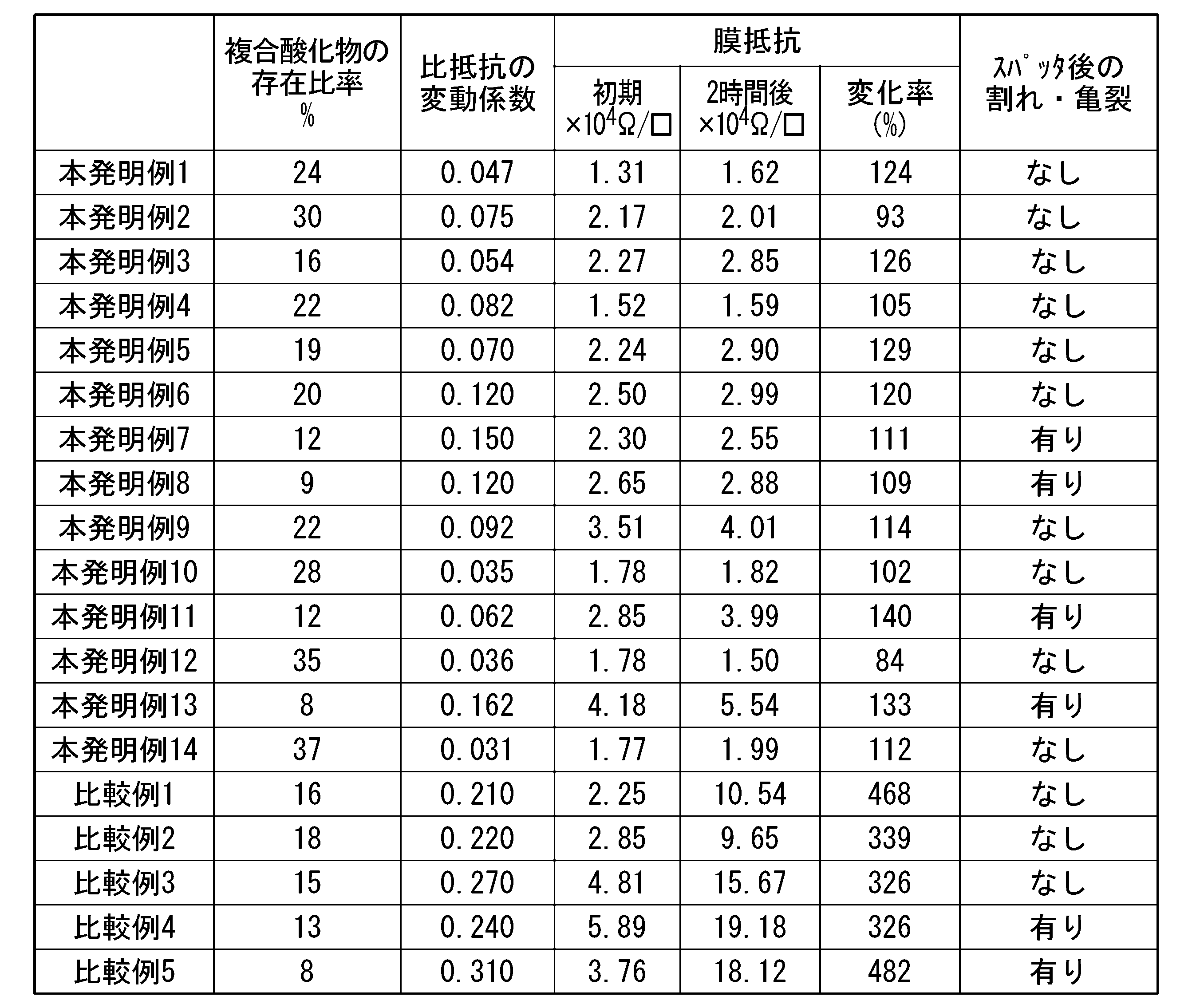
比較例1においては、仮焼成工程における焼成温度が400℃とされており、酸化物スパッタリングターゲットの比抵抗値の変動係数が0.210と大きくなった。これにより、スパッタ成膜初期に成膜された酸化物膜とスパッタ成膜開始から2時間経過時に成膜された酸化物膜とで、膜抵抗が大きく変化した。
比較例2においては、仮焼成工程における焼成温度での保持時間が1時間とされており、酸化物スパッタリングターゲットの比抵抗値の変動係数が0.220と大きくなった。これにより、スパッタ成膜初期に成膜された酸化物膜とスパッタ成膜開始から2時間経過時に成膜された酸化物膜とで、膜抵抗が大きく変化した。
比較例3においては、仮焼成工程を実施しておらず、酸化物スパッタリングターゲットの比抵抗値の変動係数が0.270と大きくなった。これにより、スパッタ成膜初期に成膜された酸化物膜とスパッタ成膜開始から2時間経過時に成膜された酸化物膜とで、膜抵抗が大きく変化した。
比較例4,5においては、仮焼成工程を実施しておらず、酸化物スパッタリングターゲットの比抵抗値の変動係数がそれぞれ0.240,0.310と大きくなった。これにより、スパッタ成膜初期に成膜された酸化物膜とスパッタ成膜開始から2時間経過時に成膜された酸化物膜とで、膜抵抗が大きく変化した。また、比較例4,5においては、比較例3に比べてGaおよびTiの含有量が少なく、複合酸化物が十分に生成しなかった。このため、スパッタ成膜後に長さ2mm以上の割れが確認された。
これに対して、本発明例1~14においては、仮焼成工程における焼成温度が600℃以上かつ1000℃以下の範囲内、焼成温度での保持時間が2時間以上かつ6時間以下の範囲内とされており、酸化物スパッタリングターゲットの比抵抗値の変動係数が0.20以下となった。これにより、スパッタ成膜初期に成膜された酸化物膜とスパッタ成膜開始から2時間経過時に成膜された酸化物膜とで膜抵抗の変化量が抑えられていた。
なお、焼結工程において焼結温度での保持時間が1時間とされた本発明例7、焼結工程において焼結温度が750℃とされた本発明例8、仮焼成工程において焼成温度が600℃とされた本発明例11、仮焼成工程において焼成温度での保持時間が2時間とされた本発明例13においては、複合酸化物が十分に生成せず、スパッタ成膜後に長さ2mm以上の割れが確認された。
以上の結果から、本発明例によれば、スパッタ成膜の初期/中期/終期で特性のばらつきが少なく均一な酸化物膜を安定して成膜可能な酸化物スパッタリングターゲット、および、この酸化物スパッタリングターゲットの製造方法を提供可能であることが確認された。
Claims (6)
- 金属成分としてZnを主成分とする酸化物焼結体からなり、
厚さ方向における比抵抗値の変動係数が0.20以下であることを特徴とする酸化物スパッタリングターゲット。 - 金属成分の合計を100原子%として、Gaが10.0原子%以上かつ20.0原子%以下、Tiが0.5原子%以上かつ5.0原子%以下、残部がZnおよび不可避不純物金属元素とされた割合で含有する酸化物からなることを特徴とする請求項1に記載の酸化物スパッタリングターゲット。
- さらに、Zr、Hf、V、Nb、Ta、Cr、Mo、W、Mn、Fe、Co、Ni、B、Al、In、Si、Ge、Sn、Pb、Sb、Bi及びランタノイド系列の元素からなる元素群より選ばれる少なくとも1種または2種以上の添加元素を合計で、金属成分の合計を100原子%として0.01原子%以上かつ10.0原子%以下の範囲内で含有することを特徴とする請求項2に記載の酸化物スパッタリングターゲット。
- 複合酸化物を有し、複合酸化物の存在比率が15%以上であることを特徴とする請求項2又は請求項3のいずれか一項に記載の酸化物スパッタリングターゲット。
- 請求項1から請求項4のいずれか一項に記載の酸化物スパッタリングターゲットを製造する酸化物スパッタリングターゲットの製造方法であって、
焼結原料粉を仮焼成する仮焼成工程と、焼成した焼結原料粉を解砕する解砕工程と、解砕した焼結原料粉を焼結して焼結体を得る焼結工程と、を備えており、
前記仮焼成工程における真空度が15Pa以下の範囲内、焼成温度が600℃以上かつ1000℃以下の範囲内、焼成温度での保持時間が2時間以上かつ6時間以下の範囲内とされていることを特徴とする酸化物スパッタリングターゲットの製造方法。 - 前記焼結工程における真空度が15Pa以下の範囲内、焼結温度が900℃以上かつ1100℃以下の範囲内、焼結温度での保持時間が2時間以上かつ6時間以下の範囲内とされていることを特徴とする請求項5に記載の酸化物スパッタリングターゲットの製造方法。
Applications Claiming Priority (2)
| Application Number | Priority Date | Filing Date | Title |
|---|---|---|---|
| JP2021000440A JP2022105853A (ja) | 2021-01-05 | 2021-01-05 | 酸化物スパッタリングターゲット、および、酸化物スパッタリングターゲットの製造方法 |
| JP2021-000440 | 2021-01-05 |
Publications (1)
| Publication Number | Publication Date |
|---|---|
| WO2022149557A1 true WO2022149557A1 (ja) | 2022-07-14 |
Family
ID=82357765
Family Applications (1)
| Application Number | Title | Priority Date | Filing Date |
|---|---|---|---|
| PCT/JP2021/048909 Ceased WO2022149557A1 (ja) | 2021-01-05 | 2021-12-28 | 酸化物スパッタリングターゲット、および、酸化物スパッタリングターゲットの製造方法 |
Country Status (2)
| Country | Link |
|---|---|
| JP (1) | JP2022105853A (ja) |
| WO (1) | WO2022149557A1 (ja) |
Citations (3)
| Publication number | Priority date | Publication date | Assignee | Title |
|---|---|---|---|---|
| JP2004244723A (ja) * | 2003-01-22 | 2004-09-02 | Canon Inc | 焼結体とそれを用いた成膜方法 |
| JP2015052165A (ja) * | 2013-08-06 | 2015-03-19 | 三菱マテリアル株式会社 | スパッタリングターゲット及びその製造方法 |
| JP2016098396A (ja) * | 2014-11-20 | 2016-05-30 | Tdk株式会社 | スパッタリングターゲット、透明導電性酸化物薄膜、及び導電性フィルム |
-
2021
- 2021-01-05 JP JP2021000440A patent/JP2022105853A/ja active Pending
- 2021-12-28 WO PCT/JP2021/048909 patent/WO2022149557A1/ja not_active Ceased
Patent Citations (3)
| Publication number | Priority date | Publication date | Assignee | Title |
|---|---|---|---|---|
| JP2004244723A (ja) * | 2003-01-22 | 2004-09-02 | Canon Inc | 焼結体とそれを用いた成膜方法 |
| JP2015052165A (ja) * | 2013-08-06 | 2015-03-19 | 三菱マテリアル株式会社 | スパッタリングターゲット及びその製造方法 |
| JP2016098396A (ja) * | 2014-11-20 | 2016-05-30 | Tdk株式会社 | スパッタリングターゲット、透明導電性酸化物薄膜、及び導電性フィルム |
Also Published As
| Publication number | Publication date |
|---|---|
| JP2022105853A (ja) | 2022-07-15 |
Similar Documents
| Publication | Publication Date | Title |
|---|---|---|
| JP4552950B2 (ja) | ターゲット用酸化物焼結体、その製造方法、それを用いた透明導電膜の製造方法、及び得られる透明導電膜 | |
| KR101741278B1 (ko) | 산화물 소결물체와 그 제조 방법, 타겟 및 투명 도전막 | |
| JP5558420B2 (ja) | スパッタリングターゲット、透明導電性酸化物、およびスパッタリングターゲットの製造方法 | |
| TWI519502B (zh) | Zn-Sn-O系氧化物燒結體及其製造方法 | |
| US10144674B2 (en) | Process for preparing ceramics, ceramics thus obtained and uses thereof, especially as a sputtering target | |
| JP5003600B2 (ja) | 酸化物焼結体、ターゲット、およびそれを用いて得られる透明導電膜、導電性積層体 | |
| JP5764828B2 (ja) | 酸化物焼結体およびそれを加工したタブレット | |
| CN108349816B (zh) | Sn-Zn-O系氧化物烧结体及其制造方法 | |
| WO2012017659A1 (ja) | スパッタリングターゲットの製造方法およびスパッタリングターゲット | |
| WO2007034733A1 (ja) | スパッタリングターゲット、透明導電膜及び透明電極 | |
| KR101990663B1 (ko) | 투명 산화물막 형성용 스퍼터링 타깃 및 그 제조 방법 | |
| JPWO2007034749A1 (ja) | 酸化物材料、及びスパッタリングターゲット | |
| EP3210952B1 (en) | Oxide sintered compact, oxide sputtering target, and oxide thin film | |
| JP2000256059A (ja) | 透明導電材料、透明導電ガラス及び透明導電フィルム | |
| JP5392633B2 (ja) | ZnO系透明導電膜用ターゲットおよびその製造方法 | |
| WO2022149557A1 (ja) | 酸化物スパッタリングターゲット、および、酸化物スパッタリングターゲットの製造方法 | |
| JP5878045B2 (ja) | 酸化亜鉛系焼結体およびその製造方法 | |
| CN1303959A (zh) | 掺铟钛酸钡材料及其制备方法 |
Legal Events
| Date | Code | Title | Description |
|---|---|---|---|
| 121 | Ep: the epo has been informed by wipo that ep was designated in this application |
Ref document number: 21917777 Country of ref document: EP Kind code of ref document: A1 |
|
| NENP | Non-entry into the national phase |
Ref country code: DE |
|
| 122 | Ep: pct application non-entry in european phase |
Ref document number: 21917777 Country of ref document: EP Kind code of ref document: A1 |