WO2022149371A1 - 電子部品 - Google Patents
電子部品 Download PDFInfo
- Publication number
- WO2022149371A1 WO2022149371A1 PCT/JP2021/043701 JP2021043701W WO2022149371A1 WO 2022149371 A1 WO2022149371 A1 WO 2022149371A1 JP 2021043701 W JP2021043701 W JP 2021043701W WO 2022149371 A1 WO2022149371 A1 WO 2022149371A1
- Authority
- WO
- WIPO (PCT)
- Prior art keywords
- resistance film
- insulating layer
- film
- wiring
- insulating
- Prior art date
- Legal status (The legal status is an assumption and is not a legal conclusion. Google has not performed a legal analysis and makes no representation as to the accuracy of the status listed.)
- Ceased
Links
Images









Classifications
-
- H—ELECTRICITY
- H10—SEMICONDUCTOR DEVICES; ELECTRIC SOLID-STATE DEVICES NOT OTHERWISE PROVIDED FOR
- H10W—GENERIC PACKAGES, INTERCONNECTIONS, CONNECTORS OR OTHER CONSTRUCTIONAL DETAILS OF DEVICES COVERED BY CLASS H10
- H10W20/00—Interconnections in chips, wafers or substrates
- H10W20/40—Interconnections external to wafers or substrates, e.g. back-end-of-line [BEOL] metallisations or vias connecting to gate electrodes
- H10W20/498—Resistive arrangements or effects of, or between, wiring layers
-
- H—ELECTRICITY
- H10—SEMICONDUCTOR DEVICES; ELECTRIC SOLID-STATE DEVICES NOT OTHERWISE PROVIDED FOR
- H10D—INORGANIC ELECTRIC SEMICONDUCTOR DEVICES
- H10D1/00—Resistors, capacitors or inductors
- H10D1/40—Resistors
- H10D1/47—Resistors having no potential barriers
- H10D1/474—Resistors having no potential barriers comprising refractory metals, transition metals, noble metals, metal compounds or metal alloys, e.g. silicides
-
- H—ELECTRICITY
- H10—SEMICONDUCTOR DEVICES; ELECTRIC SOLID-STATE DEVICES NOT OTHERWISE PROVIDED FOR
- H10W—GENERIC PACKAGES, INTERCONNECTIONS, CONNECTORS OR OTHER CONSTRUCTIONAL DETAILS OF DEVICES COVERED BY CLASS H10
- H10W20/00—Interconnections in chips, wafers or substrates
- H10W20/40—Interconnections external to wafers or substrates, e.g. back-end-of-line [BEOL] metallisations or vias connecting to gate electrodes
- H10W20/41—Interconnections external to wafers or substrates, e.g. back-end-of-line [BEOL] metallisations or vias connecting to gate electrodes characterised by their conductive parts
- H10W20/44—Conductive materials thereof
- H10W20/4403—Conductive materials thereof based on metals, e.g. alloys, metal silicides
- H10W20/4437—Conductive materials thereof based on metals, e.g. alloys, metal silicides the principal metal being a transition metal
- H10W20/4441—Conductive materials thereof based on metals, e.g. alloys, metal silicides the principal metal being a transition metal the principal metal being a refractory metal
- H10W20/4446—Refractory-metal alloys
-
- H—ELECTRICITY
- H10—SEMICONDUCTOR DEVICES; ELECTRIC SOLID-STATE DEVICES NOT OTHERWISE PROVIDED FOR
- H10W—GENERIC PACKAGES, INTERCONNECTIONS, CONNECTORS OR OTHER CONSTRUCTIONAL DETAILS OF DEVICES COVERED BY CLASS H10
- H10W72/00—Interconnections or connectors in packages
- H10W72/90—Bond pads, in general
- H10W72/921—Structures or relative sizes of bond pads
- H10W72/922—Bond pads being integral with underlying chip-level interconnections
-
- H—ELECTRICITY
- H10—SEMICONDUCTOR DEVICES; ELECTRIC SOLID-STATE DEVICES NOT OTHERWISE PROVIDED FOR
- H10W—GENERIC PACKAGES, INTERCONNECTIONS, CONNECTORS OR OTHER CONSTRUCTIONAL DETAILS OF DEVICES COVERED BY CLASS H10
- H10W72/00—Interconnections or connectors in packages
- H10W72/90—Bond pads, in general
- H10W72/921—Structures or relative sizes of bond pads
- H10W72/922—Bond pads being integral with underlying chip-level interconnections
- H10W72/9223—Bond pads being integral with underlying chip-level interconnections with redistribution layers [RDL]
-
- H—ELECTRICITY
- H10—SEMICONDUCTOR DEVICES; ELECTRIC SOLID-STATE DEVICES NOT OTHERWISE PROVIDED FOR
- H10W—GENERIC PACKAGES, INTERCONNECTIONS, CONNECTORS OR OTHER CONSTRUCTIONAL DETAILS OF DEVICES COVERED BY CLASS H10
- H10W72/00—Interconnections or connectors in packages
- H10W72/90—Bond pads, in general
- H10W72/921—Structures or relative sizes of bond pads
- H10W72/923—Bond pads having multiple stacked layers
-
- H—ELECTRICITY
- H10—SEMICONDUCTOR DEVICES; ELECTRIC SOLID-STATE DEVICES NOT OTHERWISE PROVIDED FOR
- H10W—GENERIC PACKAGES, INTERCONNECTIONS, CONNECTORS OR OTHER CONSTRUCTIONAL DETAILS OF DEVICES COVERED BY CLASS H10
- H10W72/00—Interconnections or connectors in packages
- H10W72/90—Bond pads, in general
- H10W72/941—Dispositions of bond pads
- H10W72/9415—Dispositions of bond pads relative to the surface, e.g. recessed, protruding
-
- H—ELECTRICITY
- H10—SEMICONDUCTOR DEVICES; ELECTRIC SOLID-STATE DEVICES NOT OTHERWISE PROVIDED FOR
- H10W—GENERIC PACKAGES, INTERCONNECTIONS, CONNECTORS OR OTHER CONSTRUCTIONAL DETAILS OF DEVICES COVERED BY CLASS H10
- H10W72/00—Interconnections or connectors in packages
- H10W72/90—Bond pads, in general
- H10W72/941—Dispositions of bond pads
- H10W72/942—Dispositions of bond pads relative to underlying supporting features, e.g. bond pads, RDLs or vias
-
- H—ELECTRICITY
- H10—SEMICONDUCTOR DEVICES; ELECTRIC SOLID-STATE DEVICES NOT OTHERWISE PROVIDED FOR
- H10W—GENERIC PACKAGES, INTERCONNECTIONS, CONNECTORS OR OTHER CONSTRUCTIONAL DETAILS OF DEVICES COVERED BY CLASS H10
- H10W72/00—Interconnections or connectors in packages
- H10W72/90—Bond pads, in general
- H10W72/951—Materials of bond pads
- H10W72/952—Materials of bond pads comprising metals or metalloids, e.g. PbSn, Ag or Cu
-
- H—ELECTRICITY
- H10—SEMICONDUCTOR DEVICES; ELECTRIC SOLID-STATE DEVICES NOT OTHERWISE PROVIDED FOR
- H10W—GENERIC PACKAGES, INTERCONNECTIONS, CONNECTORS OR OTHER CONSTRUCTIONAL DETAILS OF DEVICES COVERED BY CLASS H10
- H10W72/00—Interconnections or connectors in packages
- H10W72/90—Bond pads, in general
- H10W72/951—Materials of bond pads
- H10W72/953—Materials of bond pads not comprising solid metals or solid metalloids, e.g. polymers, ceramics or liquids
Definitions
- Patent Document 1 discloses a dielectric substrate and an integrated SiCr metal thin film resistor including a SiCr film formed on the dielectric substrate.
- One embodiment provides an electronic component capable of improving the reliability of a resistance film containing an alloy crystal composed of a metallic element and a non-metallic element.
- One embodiment comprises a chip having a main surface, an insulating layer laminated on the main surface, and an alloy crystal disposed within the insulating layer and composed of metallic and non-metallic elements, one side.
- a resistance film having a first end portion and a second end portion on the other side, a first wiring interposed between the main surface and the first end portion in the insulating layer, and the said in the insulating layer.
- the second wiring interposed between the main surface and the second end portion separated from the first wiring is partitioned into a region between the first wiring and the second wiring in the insulating layer, and the said.
- electronic components comprising an insulating region formed only by an insulating portion located in a thickness range between the main surface and the resistance film in the insulating layer.
- One embodiment includes a chip having a main surface, an insulating layer laminated on the main surface, and a resistance film arranged in the insulating layer and containing alloy crystals composed of metal elements and non-metal elements.
- electronic components including a plurality of top wirings arranged on the insulating layer at intervals from the peripheral edge of the resistance film to a region outside the resistance film so as not to overlap the resistance film in a plan view. do.
- a chip having a main surface is laminated on the main surface with a thickness of more than 2200 nm, and an insulation having a first end on the chip side and a second end on the opposite side to the chip.
- a layer and a resistance film comprising an alloy crystal arranged in the insulating layer so as not to be located in a thickness range of less than 2200 nm with respect to the first end and composed of metallic and non-metallic elements. Provide electronic components.
- a chip having a main surface is laminated on the main surface with a thickness of more than 2200 nm, and an insulation having a first end on the chip side and a second end on the opposite side to the chip.
- the insulating layer having only a layer and an insulator in the thickness direction of the insulating layer, and an insulating region formed in the insulating layer with a thickness of 2200 nm or more, and directly covering the insulating region.
- electronic components comprising a resistance film located in the region between the second end and the insulating region and comprising an alloy crystal composed of metallic and non-metallic elements.
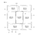
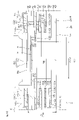
- FIG. 1 is a schematic plan view showing an electronic component according to the first embodiment.
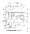
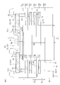
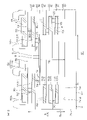
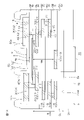
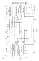
- FIG. 2 is a cross-sectional view showing a cross-sectional structure along the line II-II shown in FIG. 1 together with a resistance film according to the first embodiment.
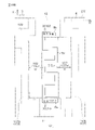
- FIG. 3 is an enlarged view of the region III shown in FIG.
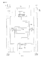
- FIG. 4 is a cross-sectional view showing a cross-sectional structure along the line II-II shown in FIG. 1 together with a resistance film according to a second embodiment.
- FIG. 5 is a cross-sectional view showing a cross-sectional structure along the line II-II shown in FIG. 1 together with a resistance film according to a third embodiment.
- FIG. 1 is a schematic plan view showing an electronic component according to the first embodiment.
- FIG. 2 is a cross-sectional view showing a cross-sectional structure along the line II-II shown in FIG. 1 together with a resistance film according to the first embodiment.
- FIG. 3 is an enlarged view of the region III
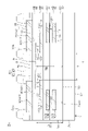
- FIG. 6 is a cross-sectional view showing a cross-sectional structure along the line II-II shown in FIG. 1 together with a resistance film according to a fourth embodiment.
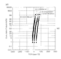
- FIG. 7 is a graph showing the sheet resistance of the resistance film.
- FIG. 8 is a graph showing the linear coefficient of the temperature coefficient of resistance of the resistance film.
- FIG. 9 is a graph showing a quadratic coefficient of the temperature coefficient of resistance of the resistance film.
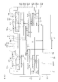
- FIG. 14 is a schematic plan view showing an electronic component according to a sixth embodiment.
- FIG. 15 is an enlarged view showing the region XV shown in FIG.
- FIG. 16 is a cross-sectional view taken along the line XVI-XVI shown in FIG.
- FIG. 17 is a cross-sectional view taken along the line XVII-XVII shown in FIG.
- FIG. 18A is an enlarged view showing the region XV shown in FIG. 14 together with the resistance film according to the second pattern.
- FIG. 18B is an enlarged view showing the region XV shown in FIG. 14 together with the resistance film according to the third pattern.
- FIG. 18C is an enlarged view showing the region XV shown in FIG. 14 together with the resistance film according to the fourth pattern.
- FIG. 19 is a graph showing the sheet resistance of the resistance film shown in FIG.
- FIG. 20 is a graph showing a linear coefficient of the temperature coefficient of resistance of the resistance film shown in FIG.
- FIG. 21 is a graph showing a quadratic coefficient of the temperature coefficient of resistance of the resistance film shown in FIG.
- FIG. 1 is a schematic plan view showing an electronic component 1 according to the first embodiment.
- FIG. 2 is a cross-sectional view showing a cross-sectional structure along the line II-II shown in FIG. 1 together with the resistance film 8 according to the first embodiment.
- FIG. 3 is an enlarged view of the region III shown in FIG.
- the electronic component 1 is, in this form, a semiconductor device including various functional devices utilizing the properties of the semiconductor.
- the electronic component 1 includes a semiconductor chip 2 (chip) formed in a rectangular cuboid shape.
- the semiconductor chip 2 has a relatively high first thermal conductivity K1.
- the semiconductor chip 2 may be a Si (silicon) chip or a WBG (wide band gap) semiconductor chip.
- the WBG semiconductor is a semiconductor having a bandgap that exceeds the bandgap of Si.
- the WBG semiconductor chip may consist of a SiC chip, a GaN chip, or a GaAs chip.
- the semiconductor chip 2 is made of a Si chip and has a first thermal conductivity K1 ( ⁇ 160 Wm ⁇ K) due to Si.
- the semiconductor chip 2 includes a first main surface 2a on one side, a second main surface 2b on the other side, and a side surface 2c connecting the first main surface 2a and the second main surface 2b.
- the first main surface 2a and the second main surface 2b are formed in a square shape in a plan view seen from their normal directions.
- the electronic component 1 includes a device area 3 provided on the first main surface 2a.
- the device region 3 is partitioned in the inner portion of the first main surface 2a at a distance from the side surface 2c in a plan view.
- the number, arrangement and shape of the device area 3 are arbitrary and are not limited to a specific number, arrangement and shape.
- the electronic component 1 includes a functional device formed in the device region 3.
- the functional device may include at least one of a semiconductor switching device, a semiconductor rectifying device and a passive device.
- JFETs Joint Field Effect Transistors
- MISFETs Metal Insulator Semiconductor Field Effect Transistors
- BJTs Bipolar Junction Transistors
- IGBTs Insulated Transistors
- It may contain at least one of (Gate Bipolar Junction Transistor).
- the semiconductor rectifying device may include at least one of a pn junction diode, a pin junction diode, a Zener diode, a Schottky barrier diode and a fast recovery diode.
- the passive device may include at least one of a resistor, a capacitor, an inductor and a fuse.
- the functional device may include a network (eg, an integrated circuit such as an LSI) in which at least two devices of a semiconductor switching device, a semiconductor rectifying device and a passive device are selectively combined.
- the electronic component 1 includes an outer region 4 provided on the first main surface 2a.
- the outer region 4 is an region outside the device region 3.
- the outer region 4 is a region in which the functional device is not included in the first main surface 2a, and is partitioned into an arbitrary position on the first main surface 2a with an arbitrary shape and an arbitrary number.
- the outer region 4 is partitioned in this form into a region between the side surface 2c and the device region 3 on the first main surface 2a.
- the outer region 4 may be partitioned on the region between the plurality of device regions 3.
- the electronic component 1 includes an insulating layer 5 laminated on the first main surface 2a.
- the insulating layer 5 covers the device region 3 and the outer region 4. That is, the insulating layer 5 has a region that covers the functional device and a region that does not cover the functional device.
- the insulating layer 5 has a second thermal conductivity K2 (K1 ⁇ K2) which is less than the first thermal conductivity K1 of the semiconductor chip 2. That is, the insulating layer 5 has a higher heat storage property than the semiconductor chip 2.
- the insulating layer 5 contains at least one of silicon oxide and silicon nitride. That is, the insulating layer 5 is caused by at least one of the thermal conductivity ( ⁇ 1.3 Wm ⁇ K) caused by silicon oxide and the thermal conductivity ( ⁇ 29.3 Wm ⁇ K) caused by silicon nitride. It has 2 thermal conductivity K2. In this form, the insulating layer 5 is made of silicon oxide and has a second thermal conductivity K2 ( ⁇ 1.3 Wm ⁇ K) due to silicon oxide.
- the insulating layer 5 has a first end 5a on one side in the thickness direction (semiconductor chip 2 side), a second end 5b on the other side in the thickness direction (opposite side to the semiconductor chip 2), and a first end 5a and a first end. It has an insulating side surface 5c connecting the two ends 5b.
- the first end 5a is connected to the semiconductor chip 2 (first main surface 2a).
- the second end 5b is formed flat so as to extend substantially parallel to the first main surface 2a, and is formed in a square shape consistent with the first main surface 2a in a plan view.
- the insulating side surface 5c extends from the peripheral edge of the second end 5b toward the semiconductor chip 2 side and is connected to the side surface 2c of the semiconductor chip 2.
- the insulating layer 5 has a predetermined thickness TA.
- the thickness TA is the distance between the first end 5a and the second end 5b.
- the thickness TA is over 2200 nm.
- the upper limit of the thickness TA is adjusted according to the specifications of the functional device, and is set to a value that does not interfere with the forming process time of the insulating layer 5.
- the thickness TA may have an upper limit of any one of 30,000 nm or less, 25,000 nm or less, 20,000 nm or less, 15,000 nm or less, 10,000 nm or less, and 5,000 nm or less.
- the thickness TA is preferably set to 3000 nm or more and 10,000 nm or less.
- the thickness TA is set to 4500 nm in this form.
- the insulating layer 5 has a laminated structure including a plurality of interlayer insulating films 6 laminated on the first main surface 2a.
- the plurality of interlayer insulating films 6 are laminated on the first main surface 2a by a CVD (chemical vapor deposition) method.
- the insulating layer 5 has the thickness TA (2200 nm ⁇ TA)
- the number of layers of the interlayer insulating film 6 is arbitrary and is not limited to a specific number of layers.
- the number of layers of the interlayer insulating film 6 is set to a general value that does not interfere with the forming process time of the insulating layer 5.
- the number of laminated interlayer insulating films 6 may be 2 or more and 25 or less.
- the number of laminated interlayer insulating films 6 is preferably 2 or more and 10 or less.
- the insulating layer 5 preferably has a laminated structure including three or more interlayer insulating films 6. It is particularly preferable that the insulating layer 5 has a laminated structure including four or more interlayer insulating films 6. In this form, the insulating layer 5 has a laminated structure including six interlayer insulating films 6.
- the six-layer interlayer insulating film 6 includes a first interlayer insulating film 6A, a second interlayer insulating film 6B, a third interlayer insulating film 6C, a fourth interlayer insulating film 6D, and a fifth interlayer insulating film in order from the first main surface 2a side. 6E and a sixth interlayer insulating film 6F are included.
- the plurality of interlayer insulating films 6 may include at least one of a silicon oxide film and a silicon nitride film, respectively. In this form, the plurality of interlayer insulating films 6 each have a single-layer structure made of a silicon oxide film. As a result, the insulating layer 5 made of silicon oxide is formed.
- the plurality of interlayer insulating films 6 may each have a thickness of 100 nm or more and 3000 nm or less. It is preferable that the plurality of interlayer insulating films 6 each have a thickness of 300 nm or more and 1500 nm or less.
- the plurality of interlayer insulating films 6 may have different thicknesses from each other, or may have equal thicknesses to each other.
- the electronic component 1 includes an insulating region 7 formed in an arbitrary region in the insulating layer 5.
- the insulating region 7 is a region having only an insulator without having a conductor film (metal film or the like) in the thickness direction of the insulating layer 5.
- the insulating region 7 is formed in a portion of the insulating layer 5 that covers the outer region 4. That is, the insulating region 7 covers the outer region 4 outside the device region 3 and does not cover the functional device. In other words, the functional device is not formed below the insulating region 7.
- the insulating region 7 is formed up to the middle portion in the thickness direction of the insulating layer 5 toward the second end 5b with the first end 5a (first main surface 2a) as a reference (zero point).
- the insulating region 7 has a laminated structure composed of a part of a plurality of interlayer insulating films 6 (in this form, the first to fifth interlayer insulating films 6A to 6E).
- the insulating region 7 has a predetermined insulating thickness TB with respect to the thickness direction of the insulating layer 5.
- the insulation thickness TB is set to 2200 nm or more.
- the upper limit of the insulation thickness TB is less than the thickness TA of the insulation layer 5 (TB ⁇ TA).
- the insulation thickness TB may have an upper limit of any one of less than 30,000 nm, 25,000 nm or less, 20,000 nm or less, 15,000 nm or less, 10,000 nm or less, and 5,000 nm or less.
- the insulating thickness TB is preferably set to 3100 nm or more.
- the insulation thickness TB is set to 3900 nm in this form.
- the electronic component 1 includes a resistance film 8 arranged in the insulating layer 5.
- the resistance film 8 is a so-called thin film resistance.
- the resistance film 8 contains alloy crystals composed of metallic elements and non-metallic elements.
- the resistance film 8 is formed through a sputtering step and a crystallization step. In the sputtering step, an alloy containing a metallic element and a non-metallic element is sprayed on the interlayer insulating film 6 to be formed by a sputtering method. As a result, the base alloy film that is the base of the resistance film 8 is formed on the interlayer insulating film 6 to be formed.
- the base alloy film immediately after film formation is in an amorphous state.
- the base alloy film is heated at a temperature (for example, a temperature of 300 ° C. or higher and 500 ° C. or lower) and time at which the base alloy film crystallizes.
- a temperature for example, a temperature of 300 ° C. or higher and 500 ° C. or lower
- the resistance film 8 made of the alloy crystal film is formed.
- the crystallization temperature and crystallization time of the base alloy film are set to a temperature and time that do not interfere with the electrical characteristics of the functional device.
- the sheet resistance Rs of the resistance film 8 is determined by the sheet resistance Rs of the alloy crystal film produced through the crystallization step.
- the type of alloy crystal constituting the resistance film 8 is arbitrary as long as the crystallization step is carried out.
- the resistance film 8 may include at least one of a CrSi film, a CrSiN film, a CrSiO film, a TaN film, and a TiN film.
- the resistance film 8 has a single-layer structure made of a CrSi film.
- the resistance film 8 may be referred to as a “CrSi resistance film”.
- the content of the metal (Cr) with respect to the total weight of the resistance film 8 (CrSi film) may be 5 wt% or more and 50 wt% or less.
- the resistance film 8 may have a thickness of 0.1 nm or more and 100 nm or less.
- the lower limit of the thickness of the resistance film 8 is preferably 0.5 nm or more.
- the lower limit of the thickness of the resistance film 8 is most preferably 1 nm or more.
- the upper limit of the thickness of the resistance film 8 is preferably 10 nm or less.
- the upper limit of the thickness of the resistance film 8 is most preferably 5 nm or less.
- the sheet resistance Rs of the resistance film 8 may be 100 ⁇ / ⁇ or more and 50,000 ⁇ / ⁇ or less.
- the sheet resistance Rs is preferably 1000 ⁇ / ⁇ or more and 10000 ⁇ / ⁇ or less.
- the sheet resistance Rs is adjusted by adjusting the thickness of the resistance film 8, the flat area of the resistance film 8, the metal content, and the like.
- the resistance film 8 is arranged on the interlayer insulating film 6 of the third layer or more (any of the third to fifth interlayer insulating films 6C to 6E), and is located below the third layer of the interlayer insulating film 6 (first). It is preferable that it is not arranged on the second interlayer insulating film 6A to 6B).
- the resistance film 8 is arranged on the interlayer insulating film 6 of the fourth layer or more (any of the fourth to fifth interlayer insulating films 6D to 6E), and is located below the fourth layer of the interlayer insulating film 6 (first). It is particularly preferable that the material is not arranged on the third interlayer insulating film 6A to 6C).
- the resistance film 8 is arranged on the fifth interlayer insulating film 6E and covered with the sixth interlayer insulating film 6F. It is preferable that the resistance film 8 exclusively occupies the interlayer insulating film 6 (in this form, the fifth interlayer insulating film 6E) to be formed. That is, it is preferable that the conductor film (metal film) other than the resistance film 8 is not arranged in the same layer as the resistance film 8.
- the resistance film 8 is arranged in the region between the second end 5b and the insulating region 7 in the insulating layer 5 and covers the insulating region 7.
- the resistance film 8 preferably directly covers the insulating region 7. That is, it is preferable that the resistance film 8 is arranged in the insulating layer 5 so as not to be located in the thickness range of less than 2200 nm with respect to the first end 5a (first main surface 2a). It is particularly preferable that the resistance film 8 is arranged in the insulating layer 5 so as not to be located in the thickness range of less than 3100 nm with respect to the first end 5a (first main surface 2a).
- the resistance film 8 is arranged in the insulating layer 5 so as not to be located in the thickness range of less than 3900 nm with respect to the first end 5a (first main surface 2a).
- the thickness between the first end 5a (first main surface 2a) and the resistance film 8 (insulation thickness TB) in the insulating layer 5 is the thickness between the second end 5b and the resistance film 8 in the insulating layer 5. It is preferable that it is more than that.
- the insulation thickness TB in this form exceeds the thickness between the second end 5b and the resistance film 8.
- the resistance film 8 faces the first main surface 2a with the insulating region 7 interposed therebetween. That is, the resistance film 8 includes a portion of the insulating layer 5 facing the first main surface 2a with a region in which the conductor film (metal film) is not arranged. Further, the resistance film 8 includes a portion that faces the outer region 4 with the insulating region 7 interposed therebetween and does not face the functional device. In this form, the resistance film 8 does not face the functional device in the thickness direction of the insulating layer 5.
- the planar shape of the resistance film 8 is arbitrary.
- the resistance film 8 may have a square shape, a rectangular shape (strip shape), a polygonal shape, a knotted shape (zigzag shape), or a shape in which these are selectively combined in a plan view.
- the electronic component 1 includes an inorganic insulating film 9 that covers the resistance film 8 in the insulating layer 5.
- the inorganic insulating film 9 is interposed in the region between the resistance film 8 and the interlayer insulating film 6 (in this form, the sixth interlayer insulating film 6F), and faces the insulating region 7 with the resistance film 8 interposed therebetween.
- the inorganic insulating film 9 preferably covers the entire area of the resistance film 8.
- the inorganic insulating film 9 has a planar shape that matches the planar shape of the resistance film 8.
- the inorganic insulating film 9 may include at least one of a silicon oxide film and a silicon nitride film. In this form, the inorganic insulating film 9 has a single-layer structure made of a silicon oxide film.
- the electronic component 1 includes a plurality of interlayer wirings 10 laminated and arranged in the thickness range of the first end 5a and the second end 5b in the insulating layer 5.
- the plurality of interlayer wires 10 are electrically connected to the corresponding functional device and / or the resistance film 8.
- the plurality of interlayer wirings 10 may electrically connect a plurality of functional devices to each other.
- the plurality of interlayer wirings 10 may electrically connect the resistance film 8 to any functional device.
- the arrangement location and routing mode of the plurality of interlayer wirings 10 are arbitrary.
- the plurality of interlayer wirings 10 are laminated and arranged within the thickness range of the first end 5a and the resistance film 8 in the insulating layer 5, and are arranged between the second end 5b and the resistance film 8 in the insulating layer 5. Not placed in the thickness range.
- the plurality of interlayer wirings 10 are respectively arranged on the corresponding interlayer insulating film 6. That is, the plurality of interlayer wirings 10 form a multilayer wiring structure with the plurality of interlayer insulating films 6 and resistance films 8.
- the number of layers of the plurality of interlayer wirings 10 is adjusted according to the number of layers of the interlayer insulating film 6.
- the plurality of interlayer wirings 10 include at least one first interlayer wiring 10A, at least one second interlayer wiring 10B, at least one third interlayer wiring 10C, and at least one fourth interlayer wiring 10D in this form.
- the first interlayer wiring 10A is arranged on the first interlayer insulating film 6A and is covered with the second interlayer insulating film 6B.
- the second interlayer wiring 10B is arranged on the second interlayer insulating film 6B and is covered with the third interlayer insulating film 6C.
- the third interlayer wiring 10C is arranged on the third interlayer insulating film 6C and is covered with the fourth interlayer insulating film 6D.
- the fourth interlayer wiring 10D is arranged on the fourth interlayer insulating film 6D and is covered with the fifth interlayer insulating film 6E.
- the plurality of interlayer wirings 10 are not arranged on the interlayer insulating film 6 (in this embodiment, the fifth interlayer insulating film 6E) in which the resistance film 8 is arranged.
- the plurality of interlayer wirings 10 include a first lower wiring 11 and a second lower wiring 12 for the resistance film 8.
- the first lower wiring 11 is arranged directly below one end of the resistance film 8.
- One end of the resistance film 8 means an electrical connection end.
- the first lower wiring 11 is composed of one of the fourth interlayer wiring 10D.
- the first lower wiring 11 is arranged along the insulating region 7 so as to partition the insulating region 7 in a plan view.
- the second lower wiring 12 is arranged directly below the other end of the resistance film 8.
- the other end of the resistance film 8 means an electrical connection end.
- the second lower wiring 12 is arranged on the same layer as the first lower wiring 11 at intervals from the first lower wiring 11.
- the second lower wiring 12 is composed of one of the fourth interlayer wiring 10D.
- the second lower wiring 12 is arranged along the insulating region 7 so as to partition the insulating region 7 in a plan view.
- the second lower wiring 12 faces the first lower wiring 11 with the insulating region 7 interposed therebetween in a plan view.
- the resistance film 8 covers the insulating region 7 and is arranged in the insulating layer 5 so as to overlap the first lower wiring 11 and the second lower wiring 12 in a plan view.
- Each of the plurality of interlayer wirings 10 has a thickness exceeding the thickness of the resistance film 8.
- the plurality of interlayer wirings 10 each have a laminated structure including a first barrier membrane 13, a main body film 14, and a second barrier membrane 15 laminated in this order from the semiconductor chip 2 side.
- the first barrier membrane 13 is made of a Ti-based metal film.
- the first barrier film 13 may have a laminated structure including a Ti film 16 and a TiN film 17 laminated in this order from the semiconductor chip 2 side.
- the main body film 14 is made of an Al-based metal film or a Cu-based metal film, and has a thickness exceeding the thickness of the first barrier film 13.
- the main body film 14 is at least one of a pure Al film (Al film having a purity of 99% or more), a pure Cu film (Al film having a purity of 99% or more), an AlCu alloy film, an AlSi alloy film, and an AlSiCu alloy film. May include.
- the second barrier film 15 is made of a Ti-based metal film and has a thickness less than the thickness of the main body film 14.
- the second barrier film 15 may have a laminated structure including a Ti film 18 and a TiN film 19 laminated in this order from the main body film 14 side.
- the electronic component 1 includes a plurality of via electrodes 20 arranged in the insulating layer 5.
- the plurality of via electrodes 20 are electrically connected to arbitrary two interlayer wirings 10 facing each other in the thickness direction.
- the plurality of via electrodes 20 include a first via electrode 21 and a second via electrode 22 for the resistance film 8.
- the first via electrode 21 is interposed between one end of the resistance film 8 and the first lower wiring 11, and is electrically connected to one end of the resistance film 8 and the first lower wiring 11.
- the second via electrode 22 is interposed between the other end of the resistance film 8 and the second lower wiring 12, and is electrically connected to the other end of the resistance film 8 and the second lower wiring 12.
- the upper end portion of the first via electrode 21 and the upper end portion of the second via electrode 22 may protrude from the main surface of the corresponding interlayer insulating film 6 (in this embodiment, the main surface of the fifth interlayer insulating film 6E).
- the resistance film 8 is formed in a film shape along the upper end portion (main surface and part of the side wall) of the first via electrode 21 and the upper end portion (part of the main surface and side wall) of the second via electrode 22. It may have a raised portion due to the upper end portion of the first via electrode 21 and the upper end portion of the second via electrode 22.
- the plurality of via electrodes 20 each have a laminated structure including a via barrier film 24 and a via body 25 laminated in this order from the inner wall of the via hole 23 formed in the corresponding interlayer insulating film 6.
- the via barrier film 24 is formed in a film shape along the inner wall of the via hole 23, and partitions the recess in the via hole 23.
- the via barrier film 24 is made of a Ti-based metal film.
- the via barrier film 24 may have a laminated structure including a Ti film 26 and a TiN film 27 laminated in this order from the inner wall of the via hole 23.
- the via body 25 is embedded in the via hole 23 with the via barrier film 24 interposed therebetween.
- the via body 25 contains W (tungsten) or Cu (copper) embedded as an integrated member in the via hole 23.
- the electronic component 1 includes a plurality of top wirings 30 arranged on the second end 5b of the insulating layer 5.
- the plurality of top wires 30 are electrically connected to the corresponding functional device and / or the resistance film 8, respectively.
- the plurality of top wirings 30 are terminal electrodes connected to conducting wires (for example, bonding wires).
- the plurality of top wirings 30 transmit an input signal from the outside to each functional device, or transmit an output signal from each functional device to the outside.
- the plurality of top wirings 30 include a first upper wiring 31 and a second upper wiring 32 for the resistance film 8.
- the first upper wiring 31 is arranged directly above the first lower wiring 11.
- the second upper wiring 32 is arranged directly above the second lower wiring 12.
- the plurality of top wirings 30 have a thickness exceeding the thickness of the plurality of interlayer wirings 10. Similar to the plurality of interlayer wirings 10, the plurality of top wirings 30 are laminated including the first barrier film 13, the main body film 14, and the second barrier membrane 15 laminated in this order from the semiconductor chip 2 side (insulating layer 5 side). Each has a structure.
- the electronic component 1 includes a plurality of long via electrodes 40 arranged in the insulating layer 5.
- the plurality of long via electrodes 40 are electrically connected to any interlayer wiring 10 and any top wiring 30 facing each other in the thickness direction.
- the long via electrode 40 is a via electrode 20 that straddles at least two interlayer insulating films 6 of the via electrodes 20.
- the plurality of long via electrodes 40 include a first long via electrode 41 and a second long via electrode 42 for the resistance film 8.
- the first long via electrode 41 is interposed in the region between the first lower wiring 11 and the first upper wiring 31, and is electrically connected to the first lower wiring 11 and the first upper wiring 31.
- the first long via electrode 41 is arranged at a distance from the resistance film 8 and extends from the second end 5b toward the first end 5a so as to cross the resistance film 8.
- the second long via electrode 42 is interposed in the region between the second lower wiring 12 and the second upper wiring 32, and is electrically connected to the second lower wiring 12 and the second upper wiring 32.
- the second long via electrode 42 is arranged at a distance from the resistance film 8 and extends from the second end 5b side toward the first end 5a side so as to cross the resistance film 8.
- the plurality of long via electrodes 40 each have a laminated structure including a via barrier film 24 and a via body 25 laminated in this order from the inner wall of the via hole 23 formed in the corresponding interlayer insulating film 6. is doing.
- the electronic component 1 includes a top insulating layer 50 that partially covers a plurality of top wirings 30 on the second end 5b of the insulating layer 5.
- the top insulating layer 50 may be referred to as a "passivation layer”.
- the top insulating layer 50 has a plurality of pad openings 50a that partially expose the inner portions of the plurality of top wirings 30, and covers the peripheral edges of the plurality of top wirings 30.
- the top insulating layer 50 has a laminated structure including a first insulating film 51 and a second insulating film 52 laminated in this order from the insulating layer 5 side.
- the first insulating film 51 may include a silicon oxide film.
- the second insulating film 52 contains an insulator different from that of the first insulating film 51.
- the second insulating film 52 may include a silicon nitride film.
- the top insulating layer 50 may have a single-layer structure composed of the first insulating film 51 or the second insulating film 52.
- FIG. 4 is a cross-sectional view showing a cross-sectional structure along the line II-II shown in FIG. 1 together with the resistance film 8 according to the second embodiment.
- the same references will be given to the structures corresponding to the structures shown in FIGS. 1 to 3, and the description thereof will be omitted.
- the insulating layer 5 includes the first to fifth interlayer insulating films 6A to 6E laminated in this order from the first main surface 2a side, and has a thickness TA of 3600 nm. ing.
- the insulating region 7 includes a laminated structure composed of a part of the first to fourth interlayer insulating films 6A to 6D, and has an insulating thickness TB of 3100 nm.
- the resistance film 8 is arranged in the insulating layer 5 so as not to be located in the thickness range of less than 3100 nm with respect to the first end 5a (first main surface 2a).
- the plurality of interlayer wirings 10 include the first to third interlayer wirings 10A to 10C.
- the plurality of interlayer wirings 10 include the first lower wiring 11 and the second lower wiring 12 for the resistance film 8 from one of the third interlayer wiring 10C in this embodiment.
- FIG. 5 is a cross-sectional view showing a cross-sectional structure along the line II-II shown in FIG. 1 together with the resistance film 8 according to the third embodiment.
- the same references will be given to the structures corresponding to the structures shown in FIGS. 1 to 3, and the description thereof will be omitted.
- the insulating layer 5 includes the first to fourth interlayer insulating films 6A to 6D laminated in this order from the first main surface 2a side, and has a thickness TA of 2700 nm. ing.
- the insulating region 7 includes a laminated structure composed of a part of the first to third interlayer insulating films 6A to 6C, and has an insulating thickness TB of 2200 nm.
- the resistance film 8 is arranged in the insulating layer 5 so as not to be located in the thickness range of less than 2200 nm with respect to the first end 5a (first main surface 2a).
- the plurality of interlayer wirings 10 include the first and second interlayer wirings 10A to 10B.
- the first lower wiring 11 and the second lower wiring 12 for the resistance film 8 are each composed of one of the second interlayer wiring 10B in this form.
- FIG. 6 is a cross-sectional view showing a cross-sectional structure along the line II-II shown in FIG. 1 together with the resistance film 8 according to the fourth embodiment.
- the same references will be given to the structures corresponding to the structures shown in FIGS. 1 to 3, and the description thereof will be omitted.
- the insulating layer 5 includes the first to third interlayer insulating films 6A to 6C laminated in this order from the first main surface 2a side, and has a thickness TA of 1900 nm. ing.
- the insulating region 7 includes a laminated structure composed of a part of the first and second interlayer insulating films 6A to 6B, and has an insulating thickness TB of 1400 nm.
- the resistance film 8 is arranged in the insulating layer 5 so as not to be located in the thickness range of less than 1400 nm with respect to the first end 5a (first main surface 2a).
- the plurality of interlayer wirings 10 include the first interlayer wiring 10A.
- the first lower wiring 11 and the second lower wiring 12 for the resistance film 8 are each composed of one of the first interlayer wiring 10A.
- the electrical characteristics of the resistance film 8 according to the first to fourth embodiments will be described with reference to FIGS. 7 to 9.
- the sheet resistance Rs the primary coefficient TCR1 of the resistance temperature coefficient (TCR: Temperature Coefficient Resistance)
- TCR2 Temperature Coefficient Resistance
- the number of samples of the resistance film 8 according to the first to fourth embodiments used for acquiring the graphs of FIGS. 7 to 9 is 68, respectively.
- FIG. 7 is a graph showing the sheet resistance Rs of the resistance film 8.
- the vertical axis shows the cumulative probability [%]
- the horizontal axis shows the sheet resistance Rs [ ⁇ / ⁇ ] of the resistance film 8.
- FIG. 7 shows the first characteristic S1, the second characteristic S2, the third characteristic S3, and the fourth characteristic S4.
- the design values of the sheet resistance Rs are 1700 ⁇ / ⁇ or more and 2300 ⁇ / ⁇ or less.
- the sheet resistance Rs falls within the range of 1970 ⁇ / ⁇ or more and 2110 ⁇ / ⁇ or less, and the median value M1 (50%) of the sheet resistance Rs is. It is about 2050 ⁇ / ⁇ .
- the sheet resistance Rs falls within the range of 1930 ⁇ / ⁇ or more and 2120 ⁇ / ⁇ or less, and the median value M1 (50%) of the sheet resistance Rs is. It is about 2050 ⁇ / ⁇ .
- the sheet resistance Rs falls within the range of 2140 ⁇ / ⁇ or more and 2230 ⁇ / ⁇ or less, and the median value M1 (50%) of the sheet resistance Rs is. It is about 2150 ⁇ / ⁇ .
- the sheet resistance Rs falls within the range of 2130 ⁇ / ⁇ or more and 2390 ⁇ / ⁇ or less, and the median value M1 (50%) of the sheet resistance Rs is. It is about 2270 ⁇ / ⁇ .
- the sheet resistance Rs depends on the arrangement of the resistance film 8, and the accuracy of the sheet resistance Rs with respect to the design value improves as the distance between the first end 5a of the insulating layer 5 and the resistance film 8 increases. Specifically, the accuracy of the sheet resistance Rs with respect to the design value is improved in the order of the fourth form example, the third form example, the second form example, and the first form example. Since the first characteristic S1 and the second characteristic S2 are almost the same, the sheet resistance Rs converges toward the design value without diverging due to the increase in the distance between the first end 5a and the resistance film 8. Have a tendency to.
- the resistance film 8 is arranged in the insulating layer 5 so as not to be located in the thickness range of less than 2200 nm with respect to the first end 5a of the insulating layer 5. According to this structure, the accuracy of the sheet resistance Rs with respect to the design value can be improved.
- the resistance film 8 preferably covers the insulating region 7 having an insulating thickness TB of 2200 nm or more.
- the resistance film 8 covers the insulating region 7 having a thickness of 3100 nm or more. According to this structure, the accuracy of the sheet resistance Rs with respect to the design value can be further improved. In this case, it is preferable that the resistance film 8 is arranged in the insulating layer 5 so as not to be located in the thickness range of less than 3100 nm with respect to the first end 5a of the insulating layer 5.
- FIG. 8 is a graph showing the primary coefficient TCR1 of the TCR of the resistance film 8.
- the vertical axis shows the cumulative probability [%]
- the horizontal axis shows the TCR primary coefficient TCR1 [ppm / ° C.].
- FIG. 8 shows the first characteristic S11, the second characteristic S12, the third characteristic S13, and the fourth characteristic S14.
- the first characteristic S11 shows the characteristics of the resistance film 8 according to the first embodiment.
- the second characteristic S12 shows the characteristics of the resistance film 8 according to the second embodiment.
- the third characteristic S13 shows the characteristics of the resistance film 8 according to the third embodiment.
- the fourth characteristic S14 shows the characteristics of the resistance film 8 according to the fourth embodiment.
- the design values of the first-order coefficient TCR1 are all -100 ppm / ° C. or higher and + 100 ppm / ° C. or lower.
- the optimum value of the first-order coefficient TCR1 is 0 ppm / ° C.
- the primary coefficient TCR1 is within the range of ⁇ 20 ppm / ° C. or higher and + 25 ppm / ° C. or lower, and the median M2 (50%) is approximately 0 ppm. / ° C.
- the first-order coefficient TCR1 according to the first characteristic S11 is within the range of ⁇ 10 ppm / ° C. or higher and + 10 ppm / ° C. or lower in the range of ⁇ 20% with respect to the median M1 (50%).
- the primary coefficient TCR1 falls within the range of ⁇ 20 ppm / ° C. or higher and + 25 ppm / ° C. or lower, and the median M2 (50%) is approximately 0 ppm. / ° C.
- the first-order coefficient TCR1 according to the second characteristic S12 is within the range of ⁇ 10 ppm / ° C. or higher and + 10 ppm / ° C. or lower in the range of ⁇ 20% with respect to the median M1 (50%).
- the primary coefficient TCR1 falls within the range of + 5 ppm / ° C. or higher and + 60 ppm / ° C. or lower, and the median M2 (50%) is + 21 ppm / ° C. Degree.
- the primary coefficient TCR1 falls within the range of +34 ppm / ° C. or higher and +84 ppm / ° C. or lower, and the median M2 (50%) is + 52 ppm / ° C. Degree.
- the primary coefficient TCR1 depends on the arrangement of the resistance film 8, and is improved as the distance between the first end 5a of the insulating layer 5 and the resistance film 8 is increased. Specifically, the first-order coefficient TCR1 is improved in the order of the fourth form example, the third form example, the second form example, and the first form example. Since the first characteristic S11 and the second characteristic S12 are almost the same, the primary coefficient TCR1 does not diverge due to the increase in the distance between the first end 5a and the resistance film 8 toward the design value. Has a tendency to converge.
- the resistance film 8 is arranged in the insulating layer 5 so as not to be located in the thickness range of less than 2200 nm with respect to the first end 5a of the insulating layer 5.
- the resistance film 8 having the primary coefficient TCR1 can be formed in the range of ⁇ 20 ppm / ° C. or higher and + 60 ppm / ° C. or lower.
- the resistance film 8 preferably covers the insulating region 7 having an insulating thickness TB of 2200 nm or more.
- the resistance film 8 is arranged in the insulating layer 5 so as not to be located in the thickness range of less than 3100 nm with respect to the first end 5a of the insulating layer 5.
- the resistance film 8 having the primary coefficient TCR1 can be formed in the range of ⁇ 20 ppm / ° C. or higher and + 25 ppm / ° C. or lower.
- the resistance film 8 covers the insulating region 7 having a thickness of 3100 nm or more.
- FIG. 9 is a graph showing the secondary coefficient TCR2 of the TCR of the resistance film 8.
- the vertical axis shows the cumulative probability [%]
- the horizontal axis shows the secondary coefficient TCR2 [ppm / ° C2 ] of the TCR of the resistance film 8.
- FIG. 9 shows the first characteristic S21, the second characteristic S22, the third characteristic S23, and the fourth characteristic S24.
- the first characteristic S21 shows the characteristics of the resistance film 8 according to the first embodiment.
- the second characteristic S22 shows the characteristics of the resistance film 8 according to the second embodiment.
- the third characteristic S23 shows the characteristics of the resistance film 8 according to the third embodiment.
- the fourth characteristic S24 shows the characteristics of the resistance film 8 according to the fourth embodiment.
- the design value of the secondary coefficient TCR2 is ⁇ 0.5 ppm / ° C. 2 or more and 0.5 ppm / ° C. 2 or less.
- the optimum value of the quadratic coefficient TCR2 is 0 ppm / ° C 2 .
- the secondary coefficient TCR2 is within the range of ⁇ 0.16 ppm / ° C. 2 or more and ⁇ 0.08 ppm / ° C. 2 or less, and the median value is M3. (50%) is about 0.13 ppm / ° C. 2 .
- the quadratic coefficient TCR2 related to the first characteristic S21 falls within the range of ⁇ 0.15 ppm / ° C. 2 or more and ⁇ 0.1 ppm / ° C. 2 or less in the range of ⁇ 20% based on the median M3 (50%). There is.
- the secondary coefficient TCR2 is within the range of ⁇ 0.16 ppm / ° C. 2 or more and ⁇ 0.10 ppm / ° C. 2 or less, and the median value is M3. (50%) is about 0.13 ppm / ° C. 2 .
- the quadratic coefficient TCR2 related to the second characteristic S22 falls within the range of ⁇ 0.15 ppm / ° C. 2 or more and ⁇ 0.1 ppm / ° C. 2 or less in the range of ⁇ 20% based on the median M3 (50%). There is.
- the secondary coefficient TCR2 is within the range of ⁇ 0.23 ppm / ° C. 2 or more and ⁇ 0.14 ppm / ° C. 2 or less, and the median value is M3. (50%) is about 0.17 ppm / ° C. 2 .
- the secondary coefficient TCR2 is within the range of ⁇ 0.32 ppm / ° C. 2 or more and ⁇ 0.19 ppm / ° C. 2 or less, and the median value is M3. (50%) is about 0.22 ppm / ° C. 2 .
- the secondary coefficient TCR2 depends on the arrangement of the resistance film 8, and is improved as the distance between the first end 5a of the insulating layer 5 and the resistance film 8 is increased. Specifically, the quadratic coefficient TCR2 is improved in the order of the fourth form example, the third form example, the second form example, and the first form example. Since the first characteristic S21 and the second characteristic S22 are almost the same, the secondary coefficient TCR2 does not diverge due to the increase in the distance between the first end 5a and the resistance film 8 toward the design value. Has a tendency to converge.
- the resistance film 8 is arranged in the insulating layer 5 so as not to be located in the thickness range of less than 2200 nm with respect to the first end 5a of the insulating layer 5.
- the resistance film 8 having the secondary coefficient TCR2 can be formed in the range of ⁇ 0.23 ppm / ° C. 2 or more and ⁇ 0.08 ppm / ° C. 2 or less.
- the resistance film 8 preferably covers the insulating region 7 having an insulating thickness TB of 2200 nm or more.
- the resistance film 8 covers the insulating region 7 having a thickness of 3100 nm or more.
- the resistance film 8 having the secondary coefficient TCR2 can be formed in the range of ⁇ 0.16 ppm / ° C. 2 or more and ⁇ 0.08 ppm / ° C. 2 or less.
- the resistance film 8 is arranged in the insulating layer 5 so as not to be located in the thickness range of less than 3100 nm with respect to the first end 5a of the insulating layer 5.
- the electrical characteristics of the resistance film 8 depend on the distance between the first end 5a (semiconductor chip 2) of the insulating layer 5 and the resistance film 8. This is because the electrical characteristics of the resistance film 8 are almost fixed in the crystallization step performed during the formation step of the resistance film 8. That is, in the crystallization step, the base alloy film that is the base of the resistance film 8 is heated at the crystallization temperature. At this time, the larger the distance between the first end 5a and the base alloy film in the insulating layer 5, the greater the heat storage effect in the region between the first end 5a and the base alloy film.
- the resistance film 8 is efficiently crystallized by utilizing the temperature rise of the insulating region 7. be able to. That is, the insulating region 7 becomes a heat storage region during the manufacturing process.
- the insulating region 7 is preferably provided on the outer region 4 side outside the device region 3. According to this structure, thermal interference of the insulating region 7 with respect to the functional device can be suppressed. Further, it is possible to suppress the resistance film 8 from electrically interfering with the functional device.
- the insulating layer 5 preferably has a second thermal conductivity K2 that is less than the first thermal conductivity K1 of the semiconductor chip 2. According to this structure, the heat storage effect of the region between the base alloy film and the semiconductor chip 2 (specifically, the semiconductor wafer that is the base of the semiconductor chip 2) in the insulating layer 5 can be improved. In other words, when the distance between the semiconductor chip 2 and the resistance film 8 becomes small, the temperature rise of the base alloy film and the insulating layer 5 is hindered due to the heat dissipation through the semiconductor chip 2, and the base alloy film is crystallized. Is suppressed. Therefore, the distance between the first end 5a and the resistance film 8 in the insulating layer 5 needs to be set to a predetermined distance or more.
- the electrical characteristics of the resistance film 8 tend to converge toward the design value without diverging due to the increase in the distance between the first end 5a and the resistance film 8. It is considered that this is because the base alloy film approaches the crystallization limit due to the heat storage effect. With reference to the evaluation results of the first embodiment and the evaluation results of the second embodiment shown in FIGS. 7 to 9, the accuracy is high when the distance between the first end 5a and the base alloy film is at least 3100 nm. It is understood that the resistance film 8 having electrical characteristics can be stably formed. Therefore, it can be said that the distance between the first end 5a and the resistance film 8 is preferably 2200 nm or more, and particularly preferably 3100 nm or more.
- the electrical characteristics of the resistance film 8 hardly change due to the thickness of the insulator covering the resistance film 8 (that is, the number of layers and the thickness of the interlayer insulating film 6 located above the resistance film 8). .. This is because the insulator covering the resistance film 8 is laminated after the step of forming the resistance film 8. Therefore, once the thickness position where the resistance film 8 (base alloy film) should be arranged is determined, the upper limit of the thickness TA of the insulating layer 5 becomes arbitrary.
- the electronic component 1 includes the semiconductor chip 2 (chip), the insulating layer 5, and the resistance film 8.
- the semiconductor chip 2 has a first main surface 2a (main surface).
- the insulating layer 5 is laminated on the first main surface 2a with a thickness of more than 2200 nm.
- the insulating layer 5 has a first end 5a on the semiconductor chip 2 side and a second end 5b on the opposite side to the semiconductor chip 2.
- the resistance film 8 contains alloy crystals composed of metallic elements and non-metallic elements.
- the resistance film 8 is arranged in the insulating layer 5 so as not to be located in the thickness range of less than 2200 nm with respect to the first end 5a. According to this structure, the reliability of the resistance film 8 can be improved.
- the same reference numerals are given to the structures corresponding to the structures described for the electronic component 1, and the description thereof will be omitted.
- the electronic component 61 includes a semiconductor chip 2, a device region 3, an outer region 4, an insulating layer 5, an insulating region 7, a resistance film 8, an inorganic insulating film 9, and a plurality of electronic components 61, similarly to the electronic component 1. It includes an interlayer wiring 10, a plurality of via electrodes 20, a plurality of top wirings 30, a plurality of long via electrodes 40, and a top insulating layer 50.
- the insulating layer 5 includes the first to sixth interlayer insulating films 6A to 6F laminated in this order from the first main surface 2a side, as in the case of the first embodiment.
- the insulating region 7 includes a laminated structure composed of a part of the first to fourth interlayer insulating films 6A to 6D, and has an insulating thickness TB of 2200 nm or more.
- the insulation thickness TB is preferably 3100 nm or more.
- the resistance film 8 is arranged in the insulating layer 5 so as to be covered with a laminated film of two or more layers of the interlayer insulating film 6.
- the resistance film 8 is arranged on the fourth interlayer insulating film 6D and covered with the fifth to sixth interlayer insulating films 6E to 6F.
- the resistance film 8 occupies the fourth interlayer insulating film 6D.
- the number of layers of the interlayer insulating film 6 covering the resistance film 8 is arbitrary, and may be three or more layers.
- the plurality of interlayer wires 10 have a thickness between the second end 5b and the resistance film 8 in the insulating layer 5 in addition to the thickness range of the first end 5a and the resistance film 8 in the insulating layer 5. It is located within the range.
- the plurality of interlayer wirings 10 include a plurality of upper interlayer wirings 62 in addition to the first to third interlayer wirings 10A to 10C.
- the first to third interlayer wirings 10A to 10C are laminated and arranged in the insulating layer 5 within the thickness range of the first end 5a and the resistance film 8, respectively.
- the first to third interlayer wirings 10A to 10C are laminated and arranged on the first to third interlayer insulating films 6A to 6C, respectively.
- the plurality of upper interlayer wirings 62 are arranged within the thickness range between the second end 5b and the resistance film 8 in the insulating layer 5.
- the upper interlayer wiring 62 is arranged on the fifth interlayer insulating film 6E and is covered with the sixth interlayer insulating film 6F.
- a plurality of upper interlayer wirings 62 are laminated within the thickness range between the second end 5b and the resistance film 8 in the insulating layer 5. It may be arranged.
- the plurality of interlayer wirings 10 include a first lower wiring 11, a second lower wiring 12, a first upper wiring 31 and a second upper wiring 32 for the resistance film 8.
- the first lower wiring 11 and the second lower wiring 12 are each composed of one of the third interlayer wiring 10C.
- the first upper wiring 31 and the second upper wiring 32 are each composed of one of the upper interlayer wiring 62. That is, in the electronic component 61, the first upper wiring 31 and the second upper wiring 32 are configured by the interlayer wiring 10 instead of the top wiring 30.
- the plurality of via electrodes 20 include a first via electrode 21 and a second via electrode 22 for the resistance film 8.
- the first via electrode 21 is interposed in the region between one end of the resistance film 8 and the first lower wiring 11, and is electrically connected to one end of the resistance film 8 and the first lower wiring 11.
- the second via electrode 22 is interposed in the region between one end of the resistance film 8 and the second lower wiring 12, and is electrically connected to the other end of the resistance film 8 and the second lower wiring 12.
- the plurality of long via electrodes 40 are electrically connected to an arbitrary interlayer wiring 10 and an arbitrary upper interlayer wiring 62 facing in the thickness direction.
- the first long via electrode 41 and the second long via electrode 42 for the resistance film 8 are included.
- the first long via electrode 41 is interposed in the region between the first lower wiring 11 and the first upper wiring 31 (upper interlayer wiring 62), and is electrically connected to the first lower wiring 11 and the first upper wiring 31.
- the second long via electrode 42 is interposed in the region between the first lower wiring 11 and the second upper wiring 32 (upper interlayer wiring 62), and is electrically connected to the second lower wiring 12 and the second upper wiring 32. There is.
- the electronic component 61 includes a plurality of top via electrodes 63.
- the plurality of top via electrodes 63 are electrically connected to an arbitrary interlayer wiring 10 (upper interlayer wiring 62) facing in the thickness direction and an arbitrary top wiring 30. Similar to the plurality of via electrodes 20, the plurality of top via electrodes 63 each have a laminated structure including a via barrier film 24 and a via body 25 laminated in this order from the inner wall of the via hole 23 formed in the corresponding interlayer insulating film 6. Have.
- the electronic component 61 also produces the same effect as that described for the electronic component 1.
- the same reference numerals are given to the structures corresponding to the structures described for the electronic component 1, and the description thereof will be omitted.
- the electronic component 71 includes a semiconductor chip 2, a device region 3, an outer region 4, an insulating layer 5, an insulating region 7, a resistance film 8, an inorganic insulating film 9, and a plurality of electronic components 71, similarly to the electronic component 1. It includes an interlayer wiring 10, a plurality of via electrodes 20, a plurality of top wirings 30, a plurality of long via electrodes 40, and a top insulating layer 50.
- the insulating layer 5 includes the first to sixth interlayer insulating films 6A to 6F laminated in this order from the first main surface 2a side, as in the case of the first embodiment.
- the insulating region 7 includes a laminated structure composed of a part of the first to fifth interlayer insulating films 6A to 6E, and has an insulating thickness TB of 2200 nm or more.
- the insulation thickness TB is preferably 3100 nm or more.
- the resistance film 8 is arranged on the fifth interlayer insulating film 6E and covered with the sixth interlayer insulating film 6F as in the case of the first embodiment.
- the resistance film 8 is arranged in the region between the second end 5b and the insulating region 7 in the insulating layer 5 and directly covers the insulating region 7.
- the resistance film 8 faces the semiconductor chip 2 (first main surface 2a) with only the insulating region 7 interposed therebetween in the insulating layer 5. That is, the resistance film 8 does not face the conductor film (metal film) in the region between the resistance film 8 and the first end 5a.
- the plurality of interlayer wirings 10 are laminated and arranged within the thickness range of the first end 5a and the resistance film 8 in the insulating layer 5, and the second end 5b and the second end 5b in the insulating layer 5. It is not arranged in the thickness range between the resistance films 8.
- the plurality of interlayer wirings 10 include the first to fourth interlayer wirings 10A to 10D.
- the plurality of interlayer wirings 10 do not have the first lower wiring 11 and the second lower wiring 12 for the resistance film 8 in this form.
- the plurality of via electrodes 20 are electrically connected to any two interlayer wirings 10 facing each other in the thickness direction.
- the plurality of top wirings 30 include a first upper wiring 31 and a second upper wiring 32 for the resistance film 8.
- the first upper wiring 31 faces one end of the resistance film 8 with a part of the insulating layer 5 sandwiched between them, and the second upper wiring 32 faces the other end of the resistance film 8 with a part of the insulating layer 5 sandwiched between them.
- the resistance film 8 covers the insulating region 7 and is arranged in the insulating layer 5 so as to overlap the first upper wiring 31 and the second upper wiring 32 in a plan view.
- the plurality of long via electrodes 40 are electrically connected to any interlayer wiring 10 and any top wiring 30 facing each other in the thickness direction.
- the electronic component 71 includes a first pad electrode 72 and a second pad electrode 73 arranged in the insulating layer 5.
- the first pad electrode 72 penetrates the inorganic insulating film 9 in the insulating layer 5 (in this form, in the sixth interlayer insulating film 6F) and is electrically connected to one end of the resistance film 8.
- the second pad electrode 73 penetrates the inorganic insulating film 9 in the insulating layer 5 (in this form, in the sixth interlayer insulating film 6F) and is electrically connected to the other end of the resistance film 8.
- the electronic component 71 includes a first pad via electrode 74 and a second pad via electrode 75 arranged in the insulating layer 5.
- the first pad via electrode 74 is interposed in the region between the first pad electrode 72 and the first upper wiring 31, and is electrically connected to the first pad electrode 72 and the first upper wiring 31.
- the second pad via electrode 75 is interposed in the region between the second pad electrode 73 and the second upper wiring 32, and is electrically connected to the second pad electrode 73 and the second upper wiring 32. Similar to the plurality of via electrodes 20, the first pad via electrode 74 and the second pad via electrode 75 have a via barrier film 24 and a via body 25 laminated in this order from the inner wall of the via hole 23 formed in the corresponding interlayer insulating film 6. Each has a laminated structure including.
- the electronic component 71 also produces the same effect as that described for the electronic component 1.
- the resistance film 8 faces the semiconductor chip 2 with only the insulating region 7 sandwiched in the thickness direction of the insulating layer 5
- a part of the interlayer wiring 10 may be interposed in the region between the first end 5a and the resistance film 8. That is, the resistance film 8 may face the insulating region 7 and a part of the conductor film (metal film) in the thickness direction of the insulating layer 5.
- the same reference numerals will be given to the structures corresponding to the structures described for the electronic component 71, and the description thereof will be omitted.
- the electronic component 81 includes a semiconductor chip 2, a device region 3, an outer region 4, an insulating layer 5, an insulating region 7, a resistance film 8, an inorganic insulating film 9, and a plurality of electronic components 81, similarly to the electronic component 71.
- Interlayer wiring 10 a plurality of via electrodes 20, a plurality of top wirings 30, a plurality of long via electrodes 40, a top insulating layer 50, a first pad electrode 72, a second pad electrode 73, a first pad via electrode 74 and a second pad via electrode 75. including.
- the insulating layer 5 includes the first to sixth interlayer insulating films 6A to 6F laminated in this order from the first main surface 2a side, as in the case of the electronic component 71.
- the insulating region 7 includes a laminated structure composed of a part of the first to fourth interlayer insulating films 6A to 6D, and has an insulating thickness TB of 2200 nm or more.
- the insulation thickness TB is preferably 3100 nm or more.
- the resistance film 8 is arranged in the insulating layer 5 so as to be covered with a laminated film of two or more layers of the interlayer insulating film 6.
- the resistance film 8 is arranged on the fourth interlayer insulating film 6D and covered with the fifth to sixth interlayer insulating films 6E to 6F.
- the resistance film 8 occupies the fourth interlayer insulating film 6D.
- the number of layers of the interlayer insulating film 6 covering the resistance film 8 is arbitrary, and may be three or more layers.
- the plurality of interlayer wires 10 have a thickness between the second end 5b and the resistance film 8 in the insulating layer 5 in addition to the thickness range of the first end 5a and the resistance film 8 in the insulating layer 5. It is located within the range.
- the plurality of interlayer wirings 10 include the upper interlayer wiring 62 in addition to the first to third interlayer wirings 10A to 10C.
- the first to third interlayer wirings 10A to 10C are laminated and arranged in the insulating layer 5 within the thickness range of the first end 5a and the resistance film 8, respectively.
- the first to third interlayer wirings 10A to 10C are laminated and arranged on the first to third interlayer insulating films 6A to 6C, respectively.
- the plurality of upper interlayer wirings 62 are arranged within the thickness range between the second end 5b and the resistance film 8 in the insulating layer 5.
- the upper interlayer wiring 62 is arranged on the fifth interlayer insulating film 6E and is covered with the sixth interlayer insulating film 6F.
- a plurality of upper interlayer wirings 62 are laminated within the thickness range between the second end 5b and the resistance film 8 in the insulating layer 5. It may be arranged.
- the plurality of interlayer wirings 10 include the first upper wiring 31 and the second upper wiring 32 for the resistance film 8.
- the first upper wiring 31 and the second upper wiring 32 are each composed of one of the upper interlayer wirings 62 in this form.
- the plurality of long via electrodes 40 are electrically connected to an arbitrary interlayer wiring 10 and an arbitrary upper interlayer wiring 62 facing in the thickness direction.
- the plurality of long via electrodes 40 include a first long via electrode 41 and a second long via electrode 42.
- the first long via electrode 41 is interposed between the arbitrary interlayer wiring 10 and the first upper wiring 31 (upper interlayer wiring 62), and is electrically connected to the arbitrary interlayer wiring 10 and the first upper wiring 31.
- the second long via electrode 42 is interposed between the arbitrary interlayer wiring 10 and the second upper wiring 32 (upper interlayer wiring 62), and is electrically connected to the arbitrary interlayer wiring 10 and the second upper wiring 32.
- the first pad electrode 72 penetrates the inorganic insulating film 9 in the insulating layer 5 (in this form, in the fifth interlayer insulating film 6E) and is electrically connected to one end of the resistance film 8.
- the second pad electrode 73 penetrates the inorganic insulating film 9 in the insulating layer 5 (in this form, in the fifth interlayer insulating film 6E) and is electrically connected to the other end of the resistance film 8.
- the first pad via electrode 74 is interposed in the region between the first pad electrode 72 and the first upper wiring 31 (upper interlayer wiring 62), and is electrically connected to the first pad electrode 72 and the first upper wiring 31.
- the second pad via electrode 75 is interposed in the region between the second pad electrode 73 and the second upper wiring 32 (upper interlayer wiring 62), and is electrically connected to the second pad electrode 73 and the second upper wiring 32. There is.
- the electronic component 81 includes a first top via electrode 82 and a second top via electrode 83 arranged in the insulating layer 5.
- the first top via electrode 82 is interposed between the first upper wiring 31 (upper interlayer wiring 62) and the arbitrary top wiring 30, and is electrically connected to the first upper wiring 31 and the arbitrary top wiring 30.
- the second top via electrode 83 is interposed between the second upper wiring 32 (upper interlayer wiring 62) and the arbitrary top wiring 30, and is electrically connected to the second upper wiring 32 and the arbitrary top wiring 30. ..
- the first top via electrode 82 and the second top via electrode 83 are the via barrier film 24 and the via body, which are laminated in this order from the inner wall of the via hole 23 formed in the corresponding interlayer insulating film 6, similarly to the plurality of via electrodes 20.
- Each has a laminated structure including 25.
- the electronic component 81 also produces the same effect as that described for the electronic component 1.
- the same reference numerals are given to the structures corresponding to the structures described for the electronic component 1, and the description thereof will be omitted.
- the insulating region 7 has an insulating thickness TB with reference to the first end 5a (zero point).
- the insulating region 7 is insulated with reference to an arbitrary interlayer wiring 10 arranged on the first end 5a side in the insulating layer 5 (zero point). It has a thickness TB.
- the insulating region 7 has an insulating thickness TB with reference to the first interlayer wiring 10A (zero point).
- the insulation thickness TB is preferably 2200 ⁇ m or more even in this case.
- the insulation thickness TB is particularly preferably 3100 nm or more.
- the insulating region 7 according to the fifth embodiment can be applied not only to the first embodiment but also to the second to fourth embodiments.
- FIG. 14 is a schematic plan view showing the electronic component 101 according to the sixth embodiment.
- FIG. 15 is an enlarged view showing the region XV shown in FIG. 14 together with the resistance film 8 according to the first pattern.
- FIG. 16 is a cross-sectional view taken along the line XVI-XVI shown in FIG.
- FIG. 17 is a cross-sectional view taken along the line XVII-XVII shown in FIG.
- the same reference numerals are given to the structures corresponding to the structures shown in FIGS. 1 to 13, and some structures are described in detail using different viewpoints and definitions from those of the first embodiment and the like. Descriptions of other structures are omitted or simplified.
- the electronic component 101 includes a semiconductor chip 2, a device region 3, and an outer region 4, as in the case of the first embodiment.
- the electronic component 101 includes a plurality of device regions 3 provided on the first main surface 2a and at least one outer region 4.
- the plurality of device regions 3 are each partitioned in the inner portion of the first main surface 2a at intervals from the side surface 2c in a plan view.
- the number, arrangement and shape of the device area 3 are arbitrary and are not limited to a specific number, arrangement and shape.
- the electronic component 101 may have a single device region 3 as in the case of the first embodiment.
- At least one outer region 4 is provided in the region between at least two device regions 3 on the first main surface 2a.
- At least one outer region 4 is provided in this form in a region partitioned from four directions by four device regions 3 in the inner portion of the first main surface 2a.
- the electronic component 101 includes an insulating layer 5 laminated on the first main surface 2a as in the case of the first embodiment.
- the insulating layer 5 includes a plurality of interlayer insulating films 6 (in this form, the first to sixth interlayer insulating films 6A to 6F) and has the above-mentioned thickness TA (2200 nm ⁇ TA).
- the insulating layer 5 covers a plurality of device regions 3 and an outer region 4.
- the plurality of interlayer insulating films 6 each have a flat outer surface in this form.
- the outer surface of each interlayer insulating film 6 is flattened by a CMP (Chemical Mechanical Polishing) method.
- the electronic component 101 includes a resistance film 8, an inorganic insulating film 9, a plurality of interlayer wirings 10 (first to fourth interlayer wirings 10A to 10D), first lower wiring 11, and second lower wiring.
- the wiring 12 and the insulating region 7 are included.
- the plurality of interlayer wirings 10 each have a laminated structure including the first barrier membrane 13, the main body film 14, and the second barrier membrane 15.
- the resistance film 8 is arranged in the insulating layer 5 as in the case of the first embodiment.
- the resistance film 8 is arranged in a portion of the insulating layer 5 that covers the outer region 4. That is, in this form, the resistance film 8 is provided in a region between at least two device regions 3 in a plan view. Specifically, the resistance film 8 is provided in a region partitioned from four directions by four device regions 3 in a plan view.
- the resistance film 8 includes a first end portion 8a on one side, a second end portion 8b on the other side, and a resistance body portion 8c between the first end portion 8a and the second end portion 8b.
- the direction in which the straight line connecting the first end portion 8a and the second end portion 8b extends is referred to as the first direction X
- the crossing direction of the first direction X (specifically, the orthogonal direction) is referred to as the second direction Y.
- the first end portion 8a and the second end portion 8b are electrical connection ends and are portions facing other members in the thickness direction of the insulating layer 5.
- the resistance main body portion 8c is located outside the first end portion 8a and the second end portion 8b, and is a portion connecting the first end portion 8a and the second end portion 8b.
- the resistance body portion 8c extends in a band shape between the first end portion 8a and the second end portion 8b. In this form, the resistance main body portion 8c extends in a straight strip shape (rectangular shape) along the first direction X.
- the width of the resistance main body 8c may be 1 ⁇ m or more and 200 ⁇ m or less.
- the width of the resistance main body 8c is the width in the direction (second direction Y) orthogonal to the direction in which the resistance main body 8c extends (first direction X).
- the first lower wiring 11 is arranged in the insulating layer 5 between the first main surface 2a and the first end portion 8a of the resistance film 8.
- the first lower wiring 11 is composed of one of the fourth interlayer wiring 10D.
- the first lower wiring 11 is drawn out from the region below the first end portion 8a of the resistance film 8 to the region outside the resistance film 8 in the direction opposite to the second end portion 8b of the resistance film 8 in a plan view. It has been.
- the first lower wiring 11 has one end located below the first end 8a of the resistance film 8 and the other end located in the region outside the resistance film 8.
- the first lower wiring 11 (one end portion) is formed wider than the resistance main body portion 8c of the resistance film 8 in the second direction Y.
- the second lower wiring 12 is arranged between the first main surface 2a and the second end portion 8b of the resistance film 8 at intervals from the first lower wiring 11 in the first direction X.
- the second lower wiring 12 is composed of one of the fourth interlayer wiring 10D.
- the second lower wiring 12 is drawn out from the region below the second end 8b of the resistance film 8 to the region outside the resistance film 8 in the direction opposite to the first end 8a of the resistance film 8 in a plan view. It has been.
- the second lower wiring 12 faces the first lower wiring 11 with a part of the insulating layer 5 interposed therebetween.
- the second lower wiring 12 has one end located below the second end 8b of the resistance film 8 and the other end located in the region outside the resistance film 8.
- the second lower wiring 12 (one end portion) is formed wider than the resistance film 8 (resistance main body portion 8c) in the second direction Y.
- the insulating region 7 is divided into a region between the first lower wiring 11 and the second lower wiring 12 in the insulating layer 5 as in the case of the first embodiment.
- the insulating region 7 is formed only by the insulating portion 7a located in the thickness range between the first main surface 2a and the resistance film 8 in the insulating layer 5.
- the insulator portion 7a is a portion having only an insulator without having a conductor film (metal film or the like) in the thickness direction of the insulating layer 5.
- the insulating portion 7a is composed of a part of a plurality of interlayer insulating films 6 (in this form, the first to fifth interlayer insulating films 6A to 6E) located in the thickness range between the first main surface 2a and the resistance film 8. It has a laminated structure.
- the insulating region 7 (insulator portion 7a) is formed in the entire area of the facing region between the first lower wiring 11 and the second lower wiring 12 in the insulating layer 5 in a plan view and a cross-sectional view. Further, the insulating region 7 is formed in the entire area of the portion where the entire area of the resistance main body portion 8c overlaps with the first main surface 2a in the plan view and the cross-sectional view.
- the insulator portion 7a in this form, is formed in a square shape including the entire resistance main body portion 8c with reference to the outermost portion of the peripheral edge of the resistance main body portion 8c in the second direction Y in a plan view. ing.
- the electronic component 101 includes a prohibited area 102 that extends the insulating area 7 to a range outside the resistance film 8.
- the prohibited area 102 is an area in which the arrangement of the conductor film (metal film or the like) is prohibited in the insulating layer 5.
- the prohibited area 102 may be referred to as an "insulated extended area".
- the prohibited region 102 includes an insulating expansion portion 102a in which the insulating portion 7a of the insulating region 7 is expanded from the peripheral edge of the resistance film 8 to a range outside the resistance film 8.
- the insulation expansion portion 102a has the insulator portion 7a in the opposite direction of the first lower wiring 11 and the second lower wiring 12 from the region between the first lower wiring 11 and the second lower wiring 12 in a plan view. It is expanded toward a direction (second direction Y) orthogonal to (first direction X).
- the prohibited area 102 expands the insulating area 7 in a square shape in a plan view.
- the insulating expansion portion 102a covers the outer region 4.
- the insulation expansion portion 102a preferably covers the outer region 4 at intervals from the plurality of device regions 3.
- the insulating extension 102a may cover at least one device region 3 across the outer region 4.
- the prohibited region 102 forms a heat storage region for the resistance film 8 as in the insulating region 7.
- the extended width W of the prohibited region 102 is preferably 2200 nm or more (2200 nm ⁇ W, TB), similarly to the insulating thickness TB of the insulating region 7.
- the extended width W is a width along the second direction Y of the prohibited region 102 when the peripheral edge of the resistance film 8 is used as a reference (zero point) in a plan view.
- the prohibited region 102 has the same effect as that of the insulating region 7 in the lateral direction along the second end 5b of the insulating layer 5.
- the extended width W may be 3100 nm or more (3100 nm ⁇ W, TB).
- the expansion width W may be the insulation thickness TB or more (TB ⁇ W) of the insulation region 7, or may be less than the insulation thickness TB (TB> W).
- the extended width W may be the thickness TA or more (TA ⁇ W) of the insulating layer 5 or may be less than the thickness TA (TA> W).
- the upper limit of the extension width W is arbitrary.
- the upper limit of the expansion width W is preferably 10 times or less (W ⁇ 10 ⁇ TB) of the insulation thickness TB in consideration of the size of the semiconductor chip 2 and the layout of the plurality of interlayer wirings 10.
- the expansion width W is particularly preferably 3.5 ⁇ m or more and 20 ⁇ m or less.
- the prohibited region 102 extends the insulation region 7 (insulator portion 7a) to a range of 3.5 ⁇ m or more and 20 ⁇ m or less from the peripheral edge of the resistance film 8 in a plan view.
- the electronic component 101 includes a plurality of third wirings 103 arranged in the insulating layer 5.
- the plurality of third wiring 103s are each composed of an interlayer wiring 10 other than the first lower wiring 11 and the second lower wiring 12.
- the plurality of third wirings 103 are arranged in layers (first to fourth interlayer insulating films 6A to 6D) other than the layer (fifth interlayer insulating film 6E) in which the resistance film 8 is arranged.
- the plurality of third wirings 103 are arranged in the insulating layer 5 apart from the resistance film 8, the first lower wiring 11, and the second lower wiring 12.
- the plurality of third wiring 103s are arranged in the insulating layer 5 at intervals from the peripheral edge of the resistance film 8 to the region outside the resistance film 8 so as not to overlap the resistance film 8 in a plan view. Specifically, the plurality of third wirings 103 are arranged in a region outside the insulating region 7 and the prohibited region 102 in a plan view, and the resistance film 8, the insulating region 7 and the prohibited region 102 sandwich a part of the insulating layer 5. Not facing.
- At least one third wiring 103 out of the plurality of third wiring 103 is arranged in the same layer as the first lower wiring 11 and the second lower wiring 12 apart from the first lower wiring 11 and the second lower wiring 12. ing. At least one of the plurality of third wiring 103s, the third wiring 103, is a layer (first to second) different from the layer (fourth interlayer insulating film 6D) in which the first lower wiring 11 and the second lower wiring 12 are arranged. It is arranged in the third interlayer insulating film 6A to 6C).
- the at least one third wiring 103 is a layer different from the first lower wiring 11 and the second lower wiring 12, and is either one of the first lower wiring 11 and the second lower wiring 12 in the thickness direction of the insulating layer 5. They may face each other.
- the plurality of third wirings 103 form at least one (plurality in this embodiment) connection wiring 103a electrically connected to either or both of the semiconductor chip 2 (specifically, the functional device) and the resistance film 8. include.
- the plurality of third wirings 103 includes a semiconductor chip 2 (specifically, a functional device) and at least one (multiple in this embodiment) dummy wiring 103b electrically separated from the resistance film 8. Specifically, the dummy wiring 103b is electrically formed in a floating state.
- the plurality of dummy wirings 103b protect the plurality of interlayer wirings 10 from undesired corrosion in the etching process for the plurality of interlayer wirings 10.
- the plurality of dummy wirings 103b protect the interlayer insulating film 6 from undesired undulations in the step of forming the interlayer insulating film 6.
- the interlayer insulating film 6 in which the undulations are suppressed is appropriately flattened by the CMP method.
- the plurality of connection wirings 103a and the plurality of dummy wirings 103b are formed on the first to fourth interlayer insulating films 6A to 6D, respectively, in this form.
- the plurality of connection wirings 103a and the plurality of dummy wirings 103b are in the same layer as the first lower wiring 11 and the second lower wiring 12, from the first lower wiring 11 and the second lower wiring 12 to the second end 5b of the insulating layer 5. They are arranged at intervals in the horizontal direction along the. In FIGS.
- connection wiring 103a is arranged on one side (left side of the paper surface), and the dummy wiring 103b is arranged on the other side (right side of the paper surface).
- the connection wiring 103a is arranged on one side (left side of the paper surface)
- the dummy wiring 103b is arranged on the other side (right side of the paper surface).
- the ratio of the total flat area of the plurality of interlayer wirings 10 (electrode films) to the outer surface of the interlayer insulating film 6 to be film-formed in a plan view is 20% or more and 80%. They are arranged on the first to fourth interlayer insulating films 6A to 6D, respectively.
- the ratio of the total flat area is preferably 25% or more and 65% or less.
- At least one third wiring 103 (interlayer wiring 10) is 1.5 times or more the width of the resistance film 8 with respect to the peripheral edge of the resistance film 8 as a reference (zero point) in the insulating region 7 and the region outside the prohibited region 102. It is arranged within the range of 4 times or less.
- the plurality of third wiring 103s are arranged so as to be separated from the peripheral edge of the resistance film 8 by 2200 nm or more according to the expansion width W of the prohibited region 102 in a plan view. It is preferable that the plurality of third wiring 103s are arranged at a distance of 3100 nm or more from the peripheral edge of the resistance film 8. It is particularly preferable that the plurality of third wiring 103s are arranged at a distance of 3.5 ⁇ m or more from the peripheral edge of the resistance film 8. It is preferable that the plurality of third wiring 103s are not arranged at a distance of 20 ⁇ m or more from the peripheral edge of the resistance film 8 in a plan view. That is, it is particularly preferable that the plurality of third wiring 103s are arranged within a range of 3.5 ⁇ m or more and 20 ⁇ m or less from the peripheral edge of the resistance film 8 in a plan view.
- the electronic component 101 has a plurality of via electrodes 20 (first via electrode 21 and second via electrode 22) and a plurality of top wirings 30 (first upper wiring 31 and second upper wiring 32). ), A plurality of long via electrodes 40 (first long via electrode 41 and second long via electrode 42), and a top insulating layer 50.
- the plurality of via electrodes 20 each have a laminated structure including a via barrier film 24 and a via body 25 laminated in this order from the inner wall of the via hole 23 formed in the corresponding interlayer insulating film 6. is doing.
- the plurality of via electrodes 20 are electrically connected to arbitrary two interlayer wirings 10 facing each other in the thickness direction, and the first via electrode 21 and the second via electrode 21 for the resistance film 8 are connected to each other.
- the via electrode 22 is included.
- the first via electrode 21 is interposed between the first end 8a of the resistance film 8 and one end of the first lower wiring 11 as in the case of the first embodiment, and is interposed between the first end 8a of the resistance film 8 and the first end 8a of the resistance film 8. It is electrically connected to one end of the first lower wiring 11.
- a plurality of first via electrodes 21 are interposed between the first end portion 8a of the resistance film 8 and one end portion of the first lower wiring 11.
- the plurality of first via electrodes 21 are arranged in a row at intervals in the second direction Y in a plan view.
- the plurality of first via electrodes 21 may be arranged in a matrix or in a staggered manner at intervals in the first direction X and the second direction Y in a plan view.
- Each first via electrode 21 may be formed in a circular shape or a polygonal shape (for example, a square shape) in a plan view.
- the number of the first via electrodes 21 is arbitrary, and a single first via electrode 21 may be arranged.
- the second via electrode 22 is interposed between the second end 8b of the resistance film 8 and one end of the second lower wiring 12, as in the case of the first embodiment, and is interposed between the second end 8b of the resistance film 8 and the second end 8b of the resistance film 8. It is electrically connected to one end of the second lower wiring 12.
- a plurality of second via electrodes 22 are interposed between the second end portion 8b of the resistance film 8 and one end portion of the second lower wiring 12.
- the plurality of second via electrodes 22 are arranged in a row at intervals in the second direction Y in a plan view.
- the plurality of second via electrodes 22 face the plurality of first via electrodes 21 with the insulating region 7 interposed therebetween in the first direction X in a plan view.
- the plurality of second via electrodes 22 may be arranged in a matrix or in a staggered manner at intervals in the first direction X and the second direction Y in a plan view.
- Each second via electrode 22 may be formed in a circular shape or a polygonal shape (for example, a square shape) in a plan view.
- the number of the second via electrodes 22 is arbitrary, and a single second via electrode 22 may be arranged.
- the plurality of top wirings 30 are laminated including the first barrier membrane 13, the main body film 14, and the second barrier membrane 15 laminated in this order from the semiconductor chip 2 side (insulating layer 5 side). Each has a structure.
- the plurality of top wirings 30 are placed on the second end 5b of the insulating layer 5 at intervals from the peripheral edge of the resistance film 8 to the region outside the resistance film 8 so as not to overlap the resistance film 8 in a plan view. Have been placed.
- the plurality of top wirings 30 are arranged in a region outside the insulating region 7 and the prohibited region 102 in a plan view, and sandwich the part of the insulating layer 5 in the resistance film 8, the insulating region 7 and the prohibited region 102. Not facing each other.
- the plurality of top wirings 30 face any interlayer wiring 10 in the thickness direction of the insulating layer 5.
- the plurality of top wirings 30 include the first upper wiring 31 and the second upper wiring 32 for the resistance film 8 as in the case of the first embodiment.
- the first upper wiring 31 is arranged in a region outside the insulating region 7 and the prohibited region 102 in a plan view, and faces the first lower wiring 11 of the lower layer with a part of the insulating layer 5 interposed therebetween.
- the first upper wiring 31 does not face the resistance film 8 in a plan view and a cross-sectional view.
- the second upper wiring 32 is arranged in a region outside the insulating region 7 and the prohibited region 102 in a plan view, and faces the second lower wiring 12 with a part of the insulating layer 5 interposed therebetween.
- the second upper wiring 32 does not face the resistance film 8 in a plan view and a cross-sectional view.
- the plurality of top wirings 30 include, in this form, at least one (plurality in this form) dummy top wiring 104 electrically separated from the semiconductor chip 2 (specifically, the functional device) and the resistance film 8.
- FIG. 17 shows an example in which a plurality of dummy top wirings 104 are arranged. Specifically, the dummy top wiring 104 is electrically formed in a floating state. The plurality of dummy top wirings 104 protect the plurality of top wirings 30 from undesired corrosion in the etching process for the plurality of top wirings 30.
- the plurality of dummy top wirings 104 are the total flat area of the plurality of top wirings 30 (electrode films) occupying the outer surface of the uppermost interlayer insulating film 6 (sixth interlayer insulating film 6F in this embodiment) to be film-formed in a plan view.
- the ratio of the total flat area is preferably 25% or more and 65% or less.
- the plurality of top wirings 30 are arranged at a distance of 2200 nm or more from the peripheral edge of the resistance film 8 according to the expansion width W of the prohibited region 102 in a plan view. It is preferable that the plurality of top wirings 30 are arranged at a distance of 3100 nm or more from the peripheral edge of the resistance film 8. It is particularly preferable that the plurality of top wirings 30 are arranged at a distance of 3.5 ⁇ m or more from the peripheral edge of the resistance film 8. It is preferable that the plurality of top wirings 30 are not arranged at a distance of 20 ⁇ m or more from the peripheral edge of the resistance film 8 in a plan view. That is, it is particularly preferable that the plurality of top wirings 30 are arranged within a range of 3.5 ⁇ m or more and 20 ⁇ m or less from the peripheral edge of the resistance film 8 in a plan view.
- the plurality of long via electrodes 40 each have a laminated structure including a via barrier film 24 and a via body 25 laminated in this order from the inner wall of the via hole 23 formed in the corresponding interlayer insulating film 6. is doing.
- the plurality of long via electrodes 40 are electrically connected to an arbitrary interlayer wiring 10 and an arbitrary top wiring 30 facing in the thickness direction, and the first long via electrode 41 for the resistance film 8 is provided.
- a second long via electrode 42 is included.
- the first long via electrode 41 is interposed in the region between the first lower wiring 11 and the first upper wiring 31, and is electrically connected to the first lower wiring 11 and the first upper wiring 31. It is connected.
- the second long via electrode 42 is interposed in the region between the second lower wiring 12 and the second upper wiring 32 as in the case of the first embodiment, and is electrically connected to the second lower wiring 12 and the second upper wiring 32. It is connected.
- the first lower wiring 11 may be electrically connected to the lower layer interlayer wiring 10 (third wiring 103) via the via electrode 20.
- the first upper wiring 31 does not necessarily have to be electrically connected to the first lower wiring 11, and any interlayer wiring 10 (third wiring 103) located in the lower layer via the first long via electrode 41. ) May be electrically connected.
- the second lower wiring 12 may be electrically connected to the lower layer interlayer wiring 10 (third wiring 103) via the via electrode 20.
- the second upper wiring 32 does not necessarily have to be electrically connected to the second lower wiring 12, and any interlayer wiring 10 (third wiring 103) located in the lower layer via the second long via electrode 42. ) May be electrically connected.
- the electronic component 101 includes a top insulating layer 50 that partially covers a plurality of top wirings 30 on the second end 5b of the insulating layer 5, as in the case of the first embodiment.
- the top insulating layer 50 has a laminated structure including the first insulating film 51 and the second insulating film 52, as in the case of the first embodiment.
- the top insulating layer 50 covers the resistance film 8, the insulating region 7, and the prohibited region 102 with a part of the insulating layer 5 interposed therebetween in the region outside the plurality of top wirings 30.
- the top insulating layer 50 may cover the entire region outside the plurality of top wirings 30 at the second end 5b of the insulating layer 5.
- the resistance film 8 may have various patterns shown in FIGS. 18A to 18C.
- 18A to 18C are enlarged views showing the region XV shown in FIG. 14 together with the resistance film 8 according to the second to fourth patterns.
- the same references will be given to the structures corresponding to the structures shown in FIGS. 14 to 17, and the description thereof will be omitted.
- the resistance film 8 is formed wider than the first lower wiring 11 and the second lower wiring 12 in this form. That is, the first lower wiring 11 and the second lower wiring 12 are formed to be narrower than the resistance film 8.
- the resistance film 8 in this form meanders the region between the first end 8a and the second end 8b in a plan view to one side and the other side of the second direction Y.
- the first lower wiring 11 and the second lower wiring 12 are formed in this form with a width exceeding the meandering width of the resistance film 8.
- the meandering width of the resistance film 8 is a meandering range along the second direction Y of the resistance film 8. That is, the first lower wiring 11 and the second lower wiring 12 are formed so that the resistance film 8 is included in the entire facing region between the first lower wiring 11 and the second lower wiring 12 in a plan view. ..
- the resistance film 8 in this form meanders the region between the first end 8a and the second end 8b in a plan view to one side and the other side of the second direction Y.
- the first lower wiring 11 and the second lower wiring 12 are formed in this form with a width less than the meandering width of the resistance film 8.
- the meandering width of the resistance film 8 is a meandering range along the second direction Y of the resistance film 8. That is, the first lower wiring 11 and the second lower wiring 12 are formed in such a manner that a part of the resistance film 8 projects from the facing region between the first lower wiring 11 and the second lower wiring 12 in a plan view. ..
- the insulating region 7 (insulator portion 7a) also has the first lower wiring 11 and the second lower wiring 12 in the insulating layer 5 in plan view and cross-sectional view. It is formed over the entire facing area between them. Further, the insulating region 7 is formed in the entire area of the portion where the entire area of the resistance main body portion 8c overlaps with the first main surface 2a in the plan view and the cross-sectional view. Further, the insulating region 7 has a square shape including the entire resistance main body 8c with respect to the outermost portion of the peripheral edge of the resistance main body 8c in the second direction Y in the plan view and the cross-sectional view. It is formed.
- the prohibited area 102 extends the insulator portion 7a toward the direction (second direction Y) orthogonal to the facing direction (first direction X) of the first lower wiring 11 and the second lower wiring 12. It has the above-mentioned expansion width W with the peripheral edge of the resistance film 8 as a reference (zero point). In this form, the prohibited area 102 extends the insulating area 7 in a square shape in a plan view.
- FIG. 19 is a graph showing the sheet resistance Rs of the resistance film 8 shown in FIG.
- the vertical axis represents the sheet resistance Rs [ ⁇ / ⁇ ]
- the horizontal axis represents the extended width W [ ⁇ m] of the prohibited region 102.
- FIG. 19 shows the sheet resistance characteristic SR when the expansion width W is changed, and the design value line L of the sheet resistance Rs.
- the sheet resistance characteristic SR when the expansion width W is changed in the range of -5 ⁇ m or more and 20 ⁇ m or less is shown.
- the zero point of the expansion width W means the peripheral edge of the resistance film 8
- the positive expansion width W means that the third wiring 103 is arranged away from the peripheral edge of the resistance film 8, and the negative expansion width W.
- the characteristics when one third wiring 103 is arranged on the interlayer insulating film 6 (third interlayer insulating film 6C) located below the resistance film 8 are shown.
- the sheet resistance characteristic SR With reference to the sheet resistance characteristic SR, it was confirmed that the sheet resistance Rs fluctuates due to the expansion width W. Specifically, the sheet resistance Rs increased with the decrease of the expansion width W, and decreased with the increase of the expansion width W. Further, it was confirmed that the sheet resistance characteristic SR tends to be saturated in the vicinity of the design value line L.
- the sheet resistance Rs showed a steep rate of change deviating from the design value line L with respect to the rate of change of the expansion width W.
- the absolute value of the slope of the tangent line of the sheet resistance characteristic SR takes the maximum value in the range where the expansion width W is negative (-5 ⁇ m ⁇ W ⁇ 0 ⁇ m).
- the sheet resistance Rs showed a slow rate of change with respect to the rate of change of the expansion width W in the vicinity of the design value line L.
- the absolute value of the slope of the tangent line of the sheet resistance characteristic SR takes the minimum value in the range where the expansion width W is positive (0 ⁇ m ⁇ W ⁇ 20 ⁇ m).
- the absolute value of the slope of the tangent line of the sheet resistance characteristic SR changed from increasing to decreasing after the expansion width W of 3.5 ⁇ m.
- the sheet resistance characteristic SR sheet resistance Rs
- the sheet resistance characteristic SR tended to converge toward the design value line L without diverging as the expansion width W increased.
- FIG. 20 is a graph showing the primary coefficient TCR1 of the TCR of the resistance film 8 shown in FIG.
- the vertical axis shows the primary coefficient TCR1 [ppm / ° C.]
- the horizontal axis shows the extended width W [ ⁇ m] of the prohibited region 102.
- FIG. 20 shows the primary characteristic ST1 and the design range R1 of the primary characteristic ST1.
- the design range R1 is ⁇ 25 ppm / ° C. or higher and 0 ppm / ° C. or lower.
- the measurement conditions are the same as in the case of the sheet resistance characteristic SR in FIG.
- the linear coefficient TCR1 fluctuates due to the expansion width W. Specifically, the first-order coefficient TCR1 increased with the decrease of the expansion width W and decreased with the increase of the expansion width W. Further, it was confirmed that the primary characteristic ST1 tends to be saturated in the design range R1.
- the linear coefficient TCR1 showed a steep rate of change deviating from the design range R1 with respect to the rate of change of the expansion width W.
- the absolute value of the slope of the tangent line of the primary characteristic ST1 takes the maximum value in the range where the expansion width W is negative (-5 ⁇ m ⁇ W ⁇ 0 ⁇ m).
- the linear coefficient TCR1 shows a slow rate of change with respect to the rate of change of the expansion width W in the vicinity of the design range R1.
- the absolute value of the slope of the tangent line of the primary characteristic ST1 takes the minimum value in the range where the expansion width W is positive (0 ⁇ m ⁇ W ⁇ 20 ⁇ m).
- the absolute value of the slope of the tangent line of the primary characteristic ST1 changed from increasing to decreasing after the expansion width W of 3.5 ⁇ m.
- the primary characteristic ST1 first-order coefficient TCR1
- the primary coefficient TCR1 of the resistance film 8 is ⁇ 25 ppm / ° C. or higher and 0 ppm / ° C. or lower.
- FIG. 21 is a graph showing the quadratic coefficient TCR2 of the TCR of the resistance film 8 shown in FIG.
- the vertical axis represents the quadratic coefficient TCR2 [ppm / ° C. 2 ]
- the horizontal axis represents the extension width W [ ⁇ m] of the prohibited region 102.
- FIG. 21 shows the secondary characteristic ST2 and the design range R2 of the secondary characteristic ST2.
- the design range R2 is ⁇ 0.15 ppm / ° C. 2 or more and 0 ppm / ° C. 2 or less.
- the measurement conditions are the same as in the case of the sheet resistance characteristic SR in FIG.
- the secondary coefficient TCR2 fluctuates due to the expansion width W. Specifically, the quadratic coefficient TCR2 decreased with the decrease of the expansion width W and increased with the increase of the expansion width W. It was also confirmed that the secondary coefficient TCR2 tends to saturate in the design range R2.
- the quadratic coefficient TCR2 showed a steep rate of change deviating from the design range R2 with respect to the rate of change of the expansion width W.
- the absolute value of the slope of the tangent line of the secondary characteristic ST2 takes the maximum value in the range where the extension width W is negative (-5 ⁇ m ⁇ W ⁇ 0 ⁇ m).
- the quadratic coefficient TCR2 shows a slow rate of change with respect to the rate of change of the expansion width W in the vicinity of the design range R2.
- the absolute value of the slope of the tangent line of the secondary characteristic ST2 takes the minimum value in the range where the extension width W is positive (0 ⁇ m ⁇ W ⁇ 20 ⁇ m).
- the absolute value of the slope of the tangent line of the secondary characteristic ST2 changed from increasing to decreasing with the expansion width W of 3.5 ⁇ m as a boundary.
- the secondary characteristic ST2 (secondary coefficient TCR2) tends to converge toward the design range R2 without diverging as the expansion width W increases.
- the secondary coefficient TCR2 of the resistance film 8 is ⁇ 0.15 ppm / ° C. 2 or more and 0 ppm / ° C. 2 or less.
- the electrical characteristics of the resistance film 8 depend on the expansion width W of the forbidden region 102 (insulation expansion portion 102a) arranged between the resistance film 8 and the third wiring 103. Is understood. This is because the electrical characteristics of the resistance film 8 are almost fixed in the crystallization step performed during the formation step of the resistance film 8. That is, in the crystallization step, the base alloy film that is the base of the resistance film 8 is heated at the crystallization temperature. At this time, as the expansion width W in the insulating layer 5 is larger, the amount of heat transferred from the insulating region 7 and the prohibited region 102 to the third wiring 103 is reduced, and the heat storage effect in the insulating region 7 and the prohibited region 102 is increased.
- the electronic component 101 includes the semiconductor chip 2, the insulating layer 5, the resistance film 8, the first lower wiring 11, the second lower wiring 12, and the insulating region 7.
- the semiconductor chip 2 has a first main surface 2a.
- the insulating layer 5 is laminated on the first main surface 2a.
- the resistance film 8 is arranged in the insulating layer 5, contains an alloy crystal composed of metallic elements and non-metallic elements, and has a first end portion 8a on one side and a second end portion 8b on the other side. ..
- the first lower wiring 11 is interposed between the first main surface 2a and the first end portion 8a of the resistance film 8 in the insulating layer 5.
- the second lower wiring 12 is interposed in the insulating layer 5 between the first main surface 2a and the second end portion 8b of the resistance film 8 so as to be separated from the first lower wiring 11 in the insulating layer 5.
- the insulating region 7 is divided into a region between the first lower wiring 11 and the second lower wiring 12 in the insulating layer 5, and is located in the thickness range between the first main surface 2a and the resistance film 8 in the insulating layer 5. It is formed only by the insulating portion 7a. According to this structure, the reliability of the resistance film 8 can be improved.
- the electronic component 101 includes a prohibited region 102 that expands the insulating region 7 to a range outside the resistance film 8 in the insulating layer 5.
- the prohibited region 102 includes an insulating expansion portion 102a in which the insulating portion 7a of the insulating region 7 is expanded from the peripheral edge of the resistance film 8 to a range outside the resistance film 8.
- the electronic component 101 includes a plurality of third wirings 103 arranged in the insulating layer 5.
- the plurality of third wirings 103 are arranged in the insulating layer 5 apart from the resistance film 8, the first lower wiring 11 and the second lower wiring 12 so as not to be located in the insulating region 7 and the prohibited region 102. According to this structure, the reliability of the resistance film 8 can be improved in the structure in which the resistance film 8, the first lower wiring 11, the second lower wiring 12, and the plurality of third wiring 103 are arranged in the insulating layer 5. ..
- the electronic component 101 includes a semiconductor chip 2, an insulating layer 5, and a plurality of top wirings 30.
- the semiconductor chip 2 has a first main surface 2a.
- the insulating layer 5 is laminated on the first main surface 2a.
- the resistance film 8 is arranged in the insulating layer 5 and contains alloy crystals composed of metallic elements and non-metallic elements.
- the plurality of top wirings 30 are arranged on the insulating layer 5 at intervals from the peripheral edge of the resistance film 8 to the region outside the resistance film 8 so as not to overlap the resistance film 8 in a plan view. According to this structure, the stress generated in the resistance film 8 due to the plurality of top wirings 30 can be relaxed. This makes it possible to suppress fluctuations in the electrical characteristics of the resistance film 8 due to the plurality of top wirings 30. Therefore, the reliability of the resistance film 8 can be improved.
- the electronic component 101 may include a first lower wiring 11, a second lower wiring 12, and an insulating region 7.
- the first lower wiring 11 is interposed between the first main surface 2a and the first end portion 8a of the resistance film 8 in the insulating layer 5.
- the second lower wiring 12 is interposed in the insulating layer 5 between the first main surface 2a and the second end portion 8b of the resistance film 8 so as to be separated from the first lower wiring 11 in the insulating layer 5.
- the insulating region 7 is divided into a region between the first lower wiring 11 and the second lower wiring 12 in the insulating layer 5, and is located in the thickness range between the first main surface 2a and the resistance film 8 in the insulating layer 5. It is formed only by the insulating portion 7a. In this case, it is preferable that the plurality of top wirings 30 are arranged in a region outside the insulating region 7 in a plan view. According to this structure, the reliability of the resistance film 8 can be improved in the structure in which the resistance film 8, the first lower wiring 11, the second lower wiring 12, and the plurality of top wirings 30 are arranged.
- the electronic component 101 includes a prohibited region 102 that expands the insulating region 7 to a range outside the resistance film 8 in the insulating layer 5.
- the prohibited region 102 includes an insulating expansion portion 102a in which the insulating portion 7a of the insulating region 7 is expanded from the peripheral edge of the resistance film 8 to a range outside the resistance film 8.
- the plurality of top wirings 30 are arranged in a region outside the insulating region 7 and the prohibited region 102 in a plan view. According to this structure, fluctuations in the electrical characteristics of the resistance film 8 due to the plurality of top wirings 30 can be appropriately suppressed.
- the electronic component 101 may include at least one third wiring 103 arranged in the insulating layer 5 away from the resistance film 8, the first lower wiring 11 and the second lower wiring 12. According to this structure, the reliability of the resistance film 8 can be improved in the structure in which the resistance film 8, the first lower wiring 11, the second lower wiring 12, the third wiring 103, and the plurality of top wirings 30 are arranged.
- the electronic component 101 may include a top insulating layer 50 that covers the insulating layer 5. It is preferable that the top insulating layer 50 partially covers the top wiring 30 on the insulating layer 5 and covers the resistance film 8 with a part of the insulating layer 5 interposed therebetween.
- At least one top wiring 30 is electrically connected to either or both of the semiconductor chip 2 (specifically, the functional device) and the resistance film 8. It is preferable that at least one top wiring 30 is formed as a dummy top wiring 104 in an electrically floating state.
- the form of the prohibited area 102, the plurality of third wiring 103, and the plurality of top wiring 30 according to the sixth embodiment is any one of the electronic components 101 according to the second to fifth embodiments in addition to the first embodiment. Can also be applied to.
- the electronic components 1, 61, 71, 81, 91 according to the second to fifth embodiments include the insulating region 7, the prohibited region 102, the plurality of third wiring 103, and the plurality of top wiring 30, respectively. 6 It has the same effect as the effect of the embodiment.
- each of the above-mentioned embodiments can be implemented in yet another embodiment.
- a plurality of resistance films 8 may be arranged in the insulating layer 5.
- the plurality of resistance films 8 are arranged in the same layer at intervals. It is particularly preferable that the plurality of resistance films 8 occupy the main surface of any one interlayer insulating film 6.
- the plurality of resistance films 8 may be arranged in a portion of the insulating layer 5 that covers the outer region 4.
- the plurality of resistance films 8 may be arranged in the same outer region 4 in a plan view, or may be arranged in different outer regions 4. In this case, it is preferable that the insulating region 7 and the prohibited region 102 are provided for each of the plurality of resistance films 8.
- the resistance film 8 is arranged in the portion of the insulating layer 5 that covers the outer region 4 .
- the resistance film 8 may be arranged in the portion of the insulating layer 5 that covers the device region 3.
- the plurality of resistance films 8 cover the resistance film 8 arranged in the portion covering the outer region 4 in the insulating layer 5 and the device region 3 in the insulating layer 5.
- Another resistance film 8 may be included in the portion. In this case, it is preferable that each of the insulating region 7 and the prohibited region 102 is provided in the device region 3.
- the electronic components 1, 61, 71, 81, 91, 101 may be decrete components containing only a single or a plurality of resistance films 8.
- an insulator chip made of glass or ceramic may be adopted instead of the semiconductor chip 2.
- the resistance film 8 according to each of the above-described embodiments may be a fuse resistance film that blows when a current exceeding the rating flows.
- a specific embodiment in this case can be obtained by replacing the "resistance film 8" with the "fuse resistance film (8)" in each of the above-described embodiments.
- the above-mentioned features of the first to sixth embodiments can be combined in any manner among them, and an electronic component having at least two features of the features of the first to sixth embodiments is adopted at the same time. May be done. That is, the features of the second embodiment may be combined with the features of the first embodiment. Further, the features of the third embodiment may be combined with any one of the features of the first to second embodiments. Further, the features of the fourth embodiment may be combined with any one of the features of the first to third embodiments. Further, the features of the fifth embodiment may be combined with any one of the features of the first to fourth embodiments. Further, the features of the sixth embodiment may be combined with any one of the features of the first to fifth embodiments.
- a chip having a main surface and an insulating layer laminated on the main surface with a thickness of more than 2200 nm and having a first end on the chip side and a second end on the opposite side to the chip.
- An electronic component comprising a resistance film comprising an alloy crystal composed of metallic and non-metallic elements, arranged in the insulating layer so as not to be located in a thickness range of less than 2200 nm with respect to the first end. ..
- A3 It has only an insulator in the thickness direction of the insulating layer, further includes an insulating region formed in the insulating layer with a thickness of 2200 nm or more, and the resistance film covers the insulating region.
- A4 Any one of A1 to A3, further including a plurality of wirings laminated and arranged in the thickness direction of the insulating layer within the thickness range between the main surface and the resistance film in the insulating layer. Electronic components described in.
- the insulating layer has a thickness of more than 3100 nm, and the resistance film is arranged in the insulating layer so as not to be located in the thickness range of less than 3100 nm with respect to the first end.
- the electronic component according to any one of A1 to A6.
- the insulating layer has a laminated structure including three or more interlayer insulating films, and the resistance film is arranged on the third or higher interlayer insulating film, any of A1 to A7. Electronic components listed in one.
- each of the interlayer insulating films has a thickness of 100 nm or more and 3000 nm or less.
- the electronic component according to A11 further including a top insulating layer that partially covers the top wiring.
- the resistance film includes at least one of a CrSi film, a CrSiN film, a CrSiO film, a TaN film, and a TiN film.
- a chip having a main surface and an insulating layer laminated on the main surface with a thickness of more than 2200 nm and having a first end on the chip side and a second end on the opposite side to the chip.
- the insulating layer so as to directly cover the insulating region having only an insulator in the thickness direction of the insulating layer and having a thickness of 2200 nm or more in the insulating layer.
- An electronic component comprising a resistance film located in the region between the two ends and the insulating region and comprising an alloy crystal composed of metallic and non-metallic elements.
- the insulating region further includes a first wiring arranged in the insulating layer and a second wiring arranged in the insulating layer at a distance from the first wiring in a plan view. It is partitioned into a region between the first wiring and the second wiring in a plan view, and the resistance film directly covers the insulating region and overlaps the first wiring and the second wiring in a plan view.
- the electronic component according to A18 which is arranged in the insulating layer.
- the semiconductor chip including the main surface and having the first thermal conductivity is laminated on the main surface with a thickness of more than 3100 nm, and the first end on the semiconductor chip side and the semiconductor chip are Any of the insulating layers including the second end on the opposite side and having a second thermal conductivity lower than the first thermal conductivity and having only an insulator in the thickness direction of the insulating layer.
- An insulating region formed in a region having a thickness of 3100 nm or more and a region between the second end and the insulating region in the insulating layer so as to directly cover the insulating region have a thickness of 0.1 nm or more and 10 nm or less.
- the insulating layer has a laminated structure including three or more interlayer insulating films, and the CrSi resistance film is arranged on the third or higher interlayer insulating film, A21 to A23.
- the semiconductor device according to any one.
- A21 to A25 further including a plurality of wirings laminated and arranged in the thickness direction of the insulating layer within the thickness range between the first end in the insulating layer and the CrSi resistance film.
- the thickness between the first end and the CrSi resistance film in the insulating layer is equal to or greater than the thickness between the second end and the CrSi resistance film in the insulating layer, A21 to A28.
- the semiconductor device according to any one of the above.
- a chip having a main surface, an insulating layer laminated on the main surface, and an alloy crystal arranged in the insulating layer and composed of a metal element and a non-metal element, the first side of which is included.
- a resistance film having one end and a second end on the other side, a first wiring interposed between the main surface and the first end in the insulating layer, and the first wiring in the insulating layer.
- the insulating layer is divided into a region between the first wiring and the second wiring in the insulating layer and the second wiring interposed between the main surface and the second end portion separated from the wiring.
- an electronic component comprising an insulating region formed only by an insulating portion located in a thickness range between the main surface and the resistance film.
- the prohibited region has an expansion width of 2200 nm or more with respect to the peripheral edge of the resistance film in a plan view, and the plurality of the third wirings are separated from the peripheral edge of the resistance film by 2200 nm or more in a plan view.
- the expanded width is 20 ⁇ m or less, and at least one of the third wirings is arranged in any one of B3 to B5 within a range of 20 ⁇ m from the peripheral edge of the resistance film in a plan view. Described electronic components.
- At least one of the third wirings is arranged in the same layer as the first wiring apart from the first wiring, and at least one of the third wirings is arranged in a layer different from the first wiring.
- the electronic component according to any one of B2 to B6.
- the insulating layer has a laminated structure in which a plurality of interlayer insulating films are laminated, and the insulator portion has a laminated structure composed of a part of the plurality of interlayer insulating films, B1.
- the electronic component according to any one of B11.
- the insulating layer has a laminated structure including three or more layers of the interlayer insulating film, and the resistance film is arranged on the third or more layers of the interlayer insulating film, according to B12. Electronic components.
- a chip having a main surface, an insulating layer laminated on the main surface, a resistance film arranged in the insulating layer and containing alloy crystals composed of metallic elements and non-metallic elements, and a flat surface.
- An electronic component comprising a plurality of top wires arranged on the insulating layer at intervals from the peripheral edge of the resistance film to a region outside the resistance film so as not to overlap the resistance film visually.
- the second wiring interposed between the other ends is partitioned into a region between the first wiring and the second wiring in the insulating layer, and between the main surface and the resistance film in the insulating layer.
- the electronic component according to B16 further comprising an insulating region formed only by an insulator portion located in a thickness range, wherein the plurality of top wirings are arranged in a region outside the insulating region in plan view.
- a plurality of insulating expansion portions including an insulating expansion portion in which the insulating portion is expanded from the peripheral edge of the resistance film to a range outside the resistance film, and a prohibited region for expanding the insulation region to a range outside the resistance film.
- the B18 further includes the resistance film, the first wiring, and the third wiring arranged in the insulating layer away from the first wiring and the second wiring so as not to be located in the insulating region and the prohibited region. Described electronic components.
- B20 Any one of B16 to B19, further comprising a top insulating film that partially covers the top wiring on the insulating layer and further covers the resistance film by sandwiching a part of the insulating layer. Electronic components listed in one.
- the [A1] to [A29] and the [B1] to [B22] can be combined in any manner between them, and the above [A1] to [A29] and the above [B1] to [B22] can be combined.
- Electronic components equipped with at least two of them at the same time may be adopted.
Landscapes
- Semiconductor Integrated Circuits (AREA)
Abstract
Description
2 半導体チップ
2a 第1主面
5 絶縁層
5a 第1端
5b 第2端
6 層間絶縁膜
7 絶縁領域
7a 絶縁体部分
8 抵抗膜
10 層間配線
11 第1下配線
12 第2下配線
21 第1ビア電極
22 第2ビア電極
30 トップ配線
50 トップ絶縁層
61 電子部品
71 電子部品
81 電子部品
91 電子部品
101 電子部品
102 禁止領域
102a 絶縁拡張部
103 第3配線
103b ダミー配線
TCR1 1次係数
TCR2 2次係数
TA 絶縁層の厚さ
TB 絶縁領域の厚さ
W 禁止領域の拡張幅
Claims (20)
- 主面を有するチップと、
前記主面の上に2200nmを超える厚さで積層され、前記チップ側の第1端、および、前記チップとは反対側の第2端を有する絶縁層と、
前記第1端を基準に2200nm未満の厚さ範囲に位置しないように前記絶縁層内に配置され、金属元素および非金属元素によって構成された合金結晶を含む抵抗膜と、を含む、電子部品。 - 前記抵抗膜は、0.1nm以上100nm以下の厚さを有している、請求項1に記載の電子部品。
- 前記絶縁層の厚さ方向に関して絶縁体のみを有し、前記絶縁層内に2200nm以上の厚さで形成された絶縁領域をさらに含み、
前記抵抗膜は、前記絶縁領域を被覆するように前記絶縁層内に配置されている、請求項1または2に記載の電子部品。 - 前記絶縁層内における前記主面および前記抵抗膜の間の厚さ範囲内において前記絶縁層の厚さ方向に積層配置された複数の配線をさらに含む、請求項1~3のいずれか一項に記載の電子部品。
- 前記配線は、前記絶縁層内において前記第2端および前記抵抗膜の間の厚さ範囲に配置されていない、請求項4に記載の電子部品。
- 前記絶縁層内において前記第1端および前記抵抗膜の間の厚さは、前記絶縁層内において前記第2端および前記抵抗膜の間の厚さ以上である、請求項1~5のいずれか一項に記載の電子部品。
- 前記絶縁層は、3100nmを超える厚さを有し、
前記抵抗膜は、前記第1端を基準に3100nm未満の厚さ範囲に位置しないように前記絶縁層内に配置されている、請求項1~6のいずれか一項に記載の電子部品。 - 前記絶縁層は、3層以上の層間絶縁膜を含む積層構造を有し、
前記抵抗膜は、3層目以上の前記層間絶縁膜の上に配置されている、請求項1~7のいずれか一項に記載の電子部品。 - 前記絶縁層は、4層以上の前記層間絶縁膜を含み、
前記抵抗膜は、4層目以上の前記層間絶縁膜の上に配置されている、請求項8に記載の電子部品。 - 各前記層間絶縁膜は、100nm以上3000nm以下の厚さを有している、請求項8または9に記載の電子部品。
- 前記第2端の上に配置されたトップ配線をさらに含む、請求項1~10のいずれか一項に記載の電子部品。
- 前記トップ配線を部分的に被覆するトップ絶縁層をさらに含む、請求項11に記載の電子部品。
- 前記抵抗膜の抵抗温度係数の1次係数は、-20ppm/℃以上+60ppm/℃以下である、請求項1~12のいずれか一項に記載の電子部品。
- 前記1次係数は、+25ppm/℃以下である、請求項13に記載の電子部品。
- 前記抵抗膜の抵抗温度係数の2次係数は、-0.23ppm/℃2以上-0.08ppm/℃2以下である、請求項1~14のいずれか一項に記載の電子部品。
- 前記2次係数は、-0.16ppm/℃2以上である、請求項15に記載の電子部品。
- 前記抵抗膜は、CrSi膜、CrSiN膜、CrSiO膜、TaN膜およびTiN膜のうちの少なくとも1つを含む、請求項1~16のいずれか一項に記載の電子部品。
- 主面を有するチップと、
前記主面の上に2200nmを超える厚さで積層され、前記チップ側の第1端、および、前記チップとは反対側の第2端を有する絶縁層と、
前記絶縁層の厚さ方向に絶縁体のみを有し、前記絶縁層内に2200nm以上の厚さで形成された絶縁領域と、
前記絶縁領域を直接被覆するように前記絶縁層内において前記第2端および前記絶縁領域の間の領域に配置され、金属元素および非金属元素によって構成された合金結晶を含む抵抗膜と、を含む、電子部品。 - 前記絶縁層内に配置された第1配線と、
平面視で前記第1配線から間隔を空けて前記絶縁層内に配置された第2配線と、をさらに含み、
前記絶縁領域は、平面視で前記第1配線および前記第2配線の間の領域に区画され、
前記抵抗膜は、前記絶縁領域を直接被覆し、かつ、平面視で前記第1配線および前記第2配線に重なるように前記絶縁層内に配置されている、請求項18に記載の電子部品。 - 前記絶縁層内で前記抵抗膜および前記第1配線の間に配置された第1ビア電極と、
前記絶縁層内で前記抵抗膜および前記第2配線の間に配置された第2ビア電極と、をさらに含む、請求項19に記載の電子部品。
Priority Applications (4)
| Application Number | Priority Date | Filing Date | Title |
|---|---|---|---|
| JP2022573941A JPWO2022149371A1 (ja) | 2021-01-08 | 2021-11-29 | |
| DE112021006302.2T DE112021006302T5 (de) | 2021-01-08 | 2021-11-29 | Elektronische komponente |
| CN202180089345.7A CN116783689A (zh) | 2021-01-08 | 2021-11-29 | 电子部件 |
| US18/347,623 US20230343702A1 (en) | 2021-01-08 | 2023-07-06 | Electronic component |
Applications Claiming Priority (4)
| Application Number | Priority Date | Filing Date | Title |
|---|---|---|---|
| JP2021-002263 | 2021-01-08 | ||
| JP2021002263 | 2021-01-08 | ||
| JP2021-073596 | 2021-04-23 | ||
| JP2021073596 | 2021-04-23 |
Related Child Applications (1)
| Application Number | Title | Priority Date | Filing Date |
|---|---|---|---|
| US18/347,623 Continuation US20230343702A1 (en) | 2021-01-08 | 2023-07-06 | Electronic component |
Publications (1)
| Publication Number | Publication Date |
|---|---|
| WO2022149371A1 true WO2022149371A1 (ja) | 2022-07-14 |
Family
ID=82357405
Family Applications (1)
| Application Number | Title | Priority Date | Filing Date |
|---|---|---|---|
| PCT/JP2021/043701 Ceased WO2022149371A1 (ja) | 2021-01-08 | 2021-11-29 | 電子部品 |
Country Status (4)
| Country | Link |
|---|---|
| US (1) | US20230343702A1 (ja) |
| JP (1) | JPWO2022149371A1 (ja) |
| DE (1) | DE112021006302T5 (ja) |
| WO (1) | WO2022149371A1 (ja) |
Cited By (1)
| Publication number | Priority date | Publication date | Assignee | Title |
|---|---|---|---|---|
| WO2024014473A1 (ja) * | 2022-07-15 | 2024-01-18 | ローム株式会社 | 半導体装置 |
Citations (3)
| Publication number | Priority date | Publication date | Assignee | Title |
|---|---|---|---|---|
| WO2016181710A1 (ja) * | 2015-05-13 | 2016-11-17 | 株式会社村田製作所 | 薄膜デバイス |
| JP2020043324A (ja) * | 2018-09-05 | 2020-03-19 | ローム株式会社 | 電子部品 |
| JP2020161703A (ja) * | 2019-03-27 | 2020-10-01 | ローム株式会社 | 薄膜抵抗およびその製造方法、ならびに、薄膜抵抗を備えた電子部品 |
Family Cites Families (3)
| Publication number | Priority date | Publication date | Assignee | Title |
|---|---|---|---|---|
| EP1938361A2 (en) | 2004-09-28 | 2008-07-02 | Koninklijke Philips Electronics N.V. | Integrated sicr metal thin film resistors for sige rf-bicmos technology |
| JP7360259B2 (ja) | 2019-06-24 | 2023-10-12 | 株式会社事業性評価研究所 | 設備評価システム、プログラム、及び方法 |
| RU2019128018A (ru) | 2019-09-05 | 2021-03-05 | Общество С Ограниченной Ответственностью "Яндекс" | Способ и система для определения ответа для цифровой задачи, выполняемой в компьютерной краудсорсинговой среде |
-
2021
- 2021-11-29 WO PCT/JP2021/043701 patent/WO2022149371A1/ja not_active Ceased
- 2021-11-29 JP JP2022573941A patent/JPWO2022149371A1/ja active Pending
- 2021-11-29 DE DE112021006302.2T patent/DE112021006302T5/de active Pending
-
2023
- 2023-07-06 US US18/347,623 patent/US20230343702A1/en active Pending
Patent Citations (3)
| Publication number | Priority date | Publication date | Assignee | Title |
|---|---|---|---|---|
| WO2016181710A1 (ja) * | 2015-05-13 | 2016-11-17 | 株式会社村田製作所 | 薄膜デバイス |
| JP2020043324A (ja) * | 2018-09-05 | 2020-03-19 | ローム株式会社 | 電子部品 |
| JP2020161703A (ja) * | 2019-03-27 | 2020-10-01 | ローム株式会社 | 薄膜抵抗およびその製造方法、ならびに、薄膜抵抗を備えた電子部品 |
Cited By (1)
| Publication number | Priority date | Publication date | Assignee | Title |
|---|---|---|---|---|
| WO2024014473A1 (ja) * | 2022-07-15 | 2024-01-18 | ローム株式会社 | 半導体装置 |
Also Published As
| Publication number | Publication date |
|---|---|
| JPWO2022149371A1 (ja) | 2022-07-14 |
| DE112021006302T5 (de) | 2023-09-21 |
| US20230343702A1 (en) | 2023-10-26 |
Similar Documents
| Publication | Publication Date | Title |
|---|---|---|
| CN1830042B (zh) | 集成薄膜电阻器与金属-绝缘体-金属电容器的方法 | |
| US11062992B2 (en) | Electronic component | |
| TWI877130B (zh) | 整合式rc架構及其製造方法 | |
| JP6120528B2 (ja) | 半導体装置およびその製造方法 | |
| JP7659539B2 (ja) | 電子部品 | |
| JP6939497B2 (ja) | 抵抗素子 | |
| US10332872B2 (en) | Thin-film device | |
| JP7340948B2 (ja) | 電子部品 | |
| US20230343702A1 (en) | Electronic component | |
| CN111263978B (zh) | 半导体装置 | |
| US11804430B2 (en) | Electronic component | |
| US11545304B2 (en) | Capacitor cluster having capacitors with different shapes | |
| JP7232679B2 (ja) | 電子部品 | |
| US9299657B2 (en) | Semiconductor device and method for manufacturing semiconductor device | |
| CN116783689A (zh) | 电子部件 | |
| JP6655469B2 (ja) | 半導体装置およびその製造方法 | |
| JP7498094B2 (ja) | 半導体装置 | |
| JP2016139711A (ja) | 半導体装置およびその製造方法 | |
| JP7440212B2 (ja) | 薄膜抵抗およびその製造方法、ならびに、薄膜抵抗を備えた電子部品 | |
| JP6895094B2 (ja) | 半導体装置 | |
| US9806020B1 (en) | Semiconductor device | |
| JP3850389B2 (ja) | 半導体装置及びその製造方法 | |
| WO2023276520A1 (ja) | 電子部品 | |
| TWI871180B (zh) | 電阻器及其製造方法 | |
| JP2025142920A (ja) | 半導体装置 |
Legal Events
| Date | Code | Title | Description |
|---|---|---|---|
| 121 | Ep: the epo has been informed by wipo that ep was designated in this application |
Ref document number: 21917593 Country of ref document: EP Kind code of ref document: A1 |
|
| ENP | Entry into the national phase |
Ref document number: 2022573941 Country of ref document: JP Kind code of ref document: A |
|
| WWE | Wipo information: entry into national phase |
Ref document number: 202180089345.7 Country of ref document: CN |
|
| WWE | Wipo information: entry into national phase |
Ref document number: 112021006302 Country of ref document: DE |
|
| 122 | Ep: pct application non-entry in european phase |
Ref document number: 21917593 Country of ref document: EP Kind code of ref document: A1 |