WO2022145084A1 - 光メモリ、光回折素子、及び、記録方法 - Google Patents
光メモリ、光回折素子、及び、記録方法 Download PDFInfo
- Publication number
- WO2022145084A1 WO2022145084A1 PCT/JP2021/030685 JP2021030685W WO2022145084A1 WO 2022145084 A1 WO2022145084 A1 WO 2022145084A1 JP 2021030685 W JP2021030685 W JP 2021030685W WO 2022145084 A1 WO2022145084 A1 WO 2022145084A1
- Authority
- WO
- WIPO (PCT)
- Prior art keywords
- nanoparticles
- optical memory
- optical
- light
- phase
- Prior art date
- Legal status (The legal status is an assumption and is not a legal conclusion. Google has not performed a legal analysis and makes no representation as to the accuracy of the status listed.)
- Ceased
Links
Images


Classifications
-
- G—PHYSICS
- G11—INFORMATION STORAGE
- G11C—STATIC STORES
- G11C13/00—Digital stores characterised by the use of storage elements not covered by groups G11C11/00, G11C23/00, or G11C25/00
- G11C13/0002—Digital stores characterised by the use of storage elements not covered by groups G11C11/00, G11C23/00, or G11C25/00 using resistive RAM [RRAM] elements
- G11C13/0004—Digital stores characterised by the use of storage elements not covered by groups G11C11/00, G11C23/00, or G11C25/00 using resistive RAM [RRAM] elements comprising amorphous/crystalline phase transition cells
-
- G—PHYSICS
- G11—INFORMATION STORAGE
- G11B—INFORMATION STORAGE BASED ON RELATIVE MOVEMENT BETWEEN RECORD CARRIER AND TRANSDUCER
- G11B7/00—Recording or reproducing by optical means, e.g. recording using a thermal beam of optical radiation by modifying optical properties or the physical structure, reproducing using an optical beam at lower power by sensing optical properties; Record carriers therefor
- G11B7/004—Recording, reproducing or erasing methods; Read, write or erase circuits therefor
- G11B7/0045—Recording
- G11B7/00454—Recording involving phase-change effects
-
- G—PHYSICS
- G02—OPTICS
- G02B—OPTICAL ELEMENTS, SYSTEMS OR APPARATUS
- G02B5/00—Optical elements other than lenses
- G02B5/18—Diffraction gratings
-
- G—PHYSICS
- G11—INFORMATION STORAGE
- G11B—INFORMATION STORAGE BASED ON RELATIVE MOVEMENT BETWEEN RECORD CARRIER AND TRANSDUCER
- G11B7/00—Recording or reproducing by optical means, e.g. recording using a thermal beam of optical radiation by modifying optical properties or the physical structure, reproducing using an optical beam at lower power by sensing optical properties; Record carriers therefor
- G11B7/002—Recording, reproducing or erasing systems characterised by the shape or form of the carrier
- G11B7/0033—Recording, reproducing or erasing systems characterised by the shape or form of the carrier with cards or other card-like flat carriers, e.g. flat sheets of optical film
-
- G—PHYSICS
- G11—INFORMATION STORAGE
- G11B—INFORMATION STORAGE BASED ON RELATIVE MOVEMENT BETWEEN RECORD CARRIER AND TRANSDUCER
- G11B7/00—Recording or reproducing by optical means, e.g. recording using a thermal beam of optical radiation by modifying optical properties or the physical structure, reproducing using an optical beam at lower power by sensing optical properties; Record carriers therefor
- G11B7/12—Heads, e.g. forming of the optical beam spot or modulation of the optical beam
- G11B7/135—Means for guiding the beam from the source to the record carrier or from the record carrier to the detector
- G11B7/1353—Diffractive elements, e.g. holograms or gratings
-
- G—PHYSICS
- G11—INFORMATION STORAGE
- G11B—INFORMATION STORAGE BASED ON RELATIVE MOVEMENT BETWEEN RECORD CARRIER AND TRANSDUCER
- G11B7/00—Recording or reproducing by optical means, e.g. recording using a thermal beam of optical radiation by modifying optical properties or the physical structure, reproducing using an optical beam at lower power by sensing optical properties; Record carriers therefor
- G11B7/12—Heads, e.g. forming of the optical beam spot or modulation of the optical beam
- G11B7/135—Means for guiding the beam from the source to the record carrier or from the record carrier to the detector
- G11B7/1365—Separate or integrated refractive elements, e.g. wave plates
- G11B7/1367—Stepped phase plates
-
- G—PHYSICS
- G11—INFORMATION STORAGE
- G11B—INFORMATION STORAGE BASED ON RELATIVE MOVEMENT BETWEEN RECORD CARRIER AND TRANSDUCER
- G11B7/00—Recording or reproducing by optical means, e.g. recording using a thermal beam of optical radiation by modifying optical properties or the physical structure, reproducing using an optical beam at lower power by sensing optical properties; Record carriers therefor
- G11B7/24—Record carriers characterised by shape, structure or physical properties, or by the selection of the material
- G11B7/2403—Layers; Shape, structure or physical properties thereof
- G11B7/24035—Recording layers
-
- G—PHYSICS
- G11—INFORMATION STORAGE
- G11B—INFORMATION STORAGE BASED ON RELATIVE MOVEMENT BETWEEN RECORD CARRIER AND TRANSDUCER
- G11B7/00—Recording or reproducing by optical means, e.g. recording using a thermal beam of optical radiation by modifying optical properties or the physical structure, reproducing using an optical beam at lower power by sensing optical properties; Record carriers therefor
- G11B7/24—Record carriers characterised by shape, structure or physical properties, or by the selection of the material
- G11B7/241—Record carriers characterised by shape, structure or physical properties, or by the selection of the material characterised by the selection of the material
- G11B7/242—Record carriers characterised by shape, structure or physical properties, or by the selection of the material characterised by the selection of the material of recording layers
- G11B7/243—Record carriers characterised by shape, structure or physical properties, or by the selection of the material characterised by the selection of the material of recording layers comprising inorganic materials only, e.g. ablative layers
-
- G—PHYSICS
- G11—INFORMATION STORAGE
- G11B—INFORMATION STORAGE BASED ON RELATIVE MOVEMENT BETWEEN RECORD CARRIER AND TRANSDUCER
- G11B7/00—Recording or reproducing by optical means, e.g. recording using a thermal beam of optical radiation by modifying optical properties or the physical structure, reproducing using an optical beam at lower power by sensing optical properties; Record carriers therefor
- G11B7/24—Record carriers characterised by shape, structure or physical properties, or by the selection of the material
- G11B7/241—Record carriers characterised by shape, structure or physical properties, or by the selection of the material characterised by the selection of the material
- G11B7/252—Record carriers characterised by shape, structure or physical properties, or by the selection of the material characterised by the selection of the material of layers other than recording layers
- G11B7/253—Record carriers characterised by shape, structure or physical properties, or by the selection of the material characterised by the selection of the material of layers other than recording layers of substrates
Definitions
- the present invention relates to an optical memory, an optical diffraction element, and a recording method.
- Patent Document 1 describes an optical memory (DVD, Blu-Ray (registered trademark) disc, etc.) that is a disc type and the shape of the recording material is a bulk & plain type. Such an optical memory is also called an optical disk. Some optical discs are read-only, some are writable only once, and some are rewritable multiple times.
- the rewritable optical disc uses a compound typified by the Ge-Sb-Te system as a recording material. These compounds are also called chalcogenide glass. Further, as an example thereof, Ge 2 Sb 2 Te 5 can be mentioned. In the following, Ge-Sb-Te compounds are simply referred to as GST.
- GST is a phase change type recording material that utilizes an amorphous phase and a crystalline phase.
- the amorphous phase is obtained by quenching the GST heated to a temperature above the melting point. Further, the crystal layer is obtained by annealing the amorphous phase at a temperature equal to or higher than the glass transition point and lower than the melting point.
- each section of the recording material is irradiated with a laser beam for writing.
- the phase change is realized by heating each section of the recording material to a predetermined temperature region by using this laser beam irradiation.
- the amorphous phase and the crystalline phase have different optical physical properties such as the refractive index, the absorptivity, and the reflectance of light. Therefore, in the optical disc, it is possible to read out whether each section of the recording material is an amorphous phase or a crystalline phase by using a laser beam for reading.
- a rewritable optical disc GST, which is a recording material, is provided on a substrate which is a disk-shaped resin so as to uniformly cover the entire effective region of the substrate.
- the rewritable optical disc adopts a plain type or a recording material having a concavo-convex structure called a groove-shaped groove or land.
- the layer of recording material is formed as a bulk-sized continuum. Therefore, the volume of the GST constituting the recording material is significantly larger than the volume of each section of the recording material.
- the energy required for the phase transition of the bulk-sized continuum itself is high, and the heat generated by absorbing the laser beam spreads outside the irradiation spot due to heat conduction and is easily lost. It requires high light power and / or energy to make it less energy efficient.
- One aspect of the present invention has been made in view of the above-mentioned problems, and an object thereof is to improve energy efficiency when phase-changing each section in an optical memory.
- the optical memory is composed of a support and a plurality of phase changing materials that change phase between a crystalline phase and an amorphous phase by irradiation with light. It comprises a plurality of nanoparticles that are nanoparticles and are supported by the support. In this optical memory, the nanoparticles are separated from each other in at least one of the in-plane direction of the specific surface and the normal direction of the specific surface.
- the optical diffraction element includes a plurality of cells in which the thickness or the refractive index are set independently of each other, and any of the above-mentioned first to fifth aspects.
- the optical memory according to one aspect includes an optical memory stacked in the plurality of cells. In this optical diffractive element, each of the regions obtained by projecting the bottom surface of each cell onto the specific surface is used as a partition of the optical memory, and each partition is one or a plurality of nanoparticles that are a part of the plurality of nanoparticles. Nanoparticles are arranged.
- the recording method comprises a plurality of nanoparticles composed of a phase changing material that undergoes a phase change between a crystalline phase and an amorphous phase by irradiation with light. Therefore, it is a recording method using an optical memory having a plurality of nanoparticles separated from each other in a specific in-plane direction.
- a first step in which a plurality of signal lights having a spatial intensity distribution representing specific information, each of which has a time difference, is incident on the optical memory, and a light for writing each signal light.
- the second step of recording each signal light in the optical memory is included.
- FIG. 7 It is an enlarged perspective view of a part of the optical memory which concerns on 1st Embodiment of this invention. It is sectional drawing of the optical memory shown in FIG. It is sectional drawing of the optical memory which is a modification of the optical memory shown in FIG. It is a perspective view of the light diffraction element which concerns on 2nd Embodiment of this invention. It is an enlarged perspective view of a part of the light diffraction element shown in FIG. FIG. 3 is an enlarged plan view of a part of the optical diffraction element shown in FIG. 4. It is a perspective view of the recording system which concerns on 3rd Embodiment of this invention. It is a flowchart of the recording method executed by the recording system shown in FIG. 7.
- FIG. 1 It is a schematic diagram which illustrates the information recorded by the recording method shown in FIG. It is a perspective view of an optical arithmetic unit and an optical memory constituting the recording system which is a modification of the recording system which concerns on 3rd Embodiment of this invention.
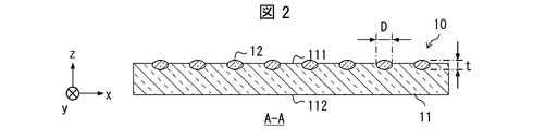
- FIG. 1 is an enlarged perspective view of a part of the optical memory 10.
- FIG. 2 is an enlarged cross-sectional view of a part of the optical memory 10, and is a cross-sectional view taken along the line AA shown in FIG.
- the optical memory 10 includes a support 11 and a plurality of nanoparticles 12.
- the support 11 is a two-dimensionally extending layered member.
- the main surfaces 111 and 112, which are a pair of main surfaces of the support 11, are parallel to the xy plane, that is, the normal direction of the main surfaces 111 and 112 is parallel to the z-axis direction.
- the orthogonal coordinate system is defined in.
- the main surface 111 is an example of a specific surface
- the in-plane direction of the main surface 111 is an example of a specific in-plane direction.
- the direction parallel to the z-axis direction is an example of the normal direction of a specific surface.
- the normal direction of a specific surface is referred to as a thickness direction.
- the thickness of the support 11 is not limited and can be appropriately determined.
- the support 11 is shown in an independent state without being supported by other members (for example, a substrate).
- the support 11 may be independent of other members or may be supported by other members such as a substrate.
- the support 11 can be supported by using the substrate.
- the support 11 is preferably made of a translucent material.
- a methacrylic resin is used as the material constituting the support 11.
- the translucent material is not limited to the methacrylic resin, and general vinyl resins, polyimides, polyethers, polyesters, polyols, epoxies, olefins, and alicyclic olefins. It may be a kind or the like.
- the material having translucency may be glass typified by quartz glass.
- the material constituting the support 11 also has translucency.
- the support 11 is arranged along the plane so that the main surfaces 111 and 112 are parallel to the xy plane.
- the support 11 may be arranged along a curved surface.
- Each of the plurality of nanoparticles 12 functions as a recording material for recording the material non-volatilely in the optical memory 10.
- Each nanoparticles 12 are composed of a phase change material that undergoes a phase change between a crystalline phase and an amorphous phase upon irradiation with light.
- Ge 2 Sb 2 Te 5 is used as a material constituting each nanoparticles 12.
- Ge 2 Sb 2 Te 5 is an example of a Ge-Sb-Te system compound also called chalcogenide glass.
- the Ge-Sb-Te system compound is simply referred to as GST
- the Ge 2 Sb 2 Te 5 is referred to as GST 225.
- GST225 has translucency.
- the material constituting each nanoparticles 12 is not limited to GST225.
- the material constituting each nanoparticles 12 can be appropriately selected from the phase change materials that undergo a phase change between the two phases due to the energy of light and / or heat, and other than pseudo-two-dimensional compounds such as GST.
- a binary compound such as Sb-Te and a multidimensional compound obtained by adding a small amount of Ge, Ag, In or the like to the binary compound can also be preferably used.
- As the multidimensional compound Ag-In-Sb-Te (AIST), Ge-Sb-Se-Te (GSST) and the like are preferably used.
- the phase change material can be appropriately selected from materials used as recording materials such as rewritable DVDs and Blu-Ray (registered trademark) discs.
- GST225 can take an amorphous phase and a crystalline phase depending on the temperature history of exposure.
- an amorphous phase is obtained.
- a crystal layer is obtained by annealing the amorphous phase at a temperature of the glass transition point Tg or more and the melting point Tm or less.
- each nanoparticle 12 is irradiated with light for writing, as in the case of an optical disc.
- the light for writing is also referred to as signal light.
- the phase change is realized by heating each nanoparticles 12 to a predetermined temperature region using this signal light.
- each nanoparticle 12 is an amorphous phase or a crystalline phase by using light for reading.
- the diameter D is the particle size of each nanoparticles 12 in a specific in-plane direction.
- the diameter D is preferably small, for example, 50 nm or less.
- the diameter D is not limited to these examples, and can be appropriately selected within the range included in the order of nanometers, that is, within the range of 1 nm or more and less than 1000 nm.
- the shape of each nanoparticles 12 in a specific in-plane direction is not circular, the diameter of the circumscribed circle of each nanoparticles 12 can be used as the diameter D.
- the thickness t of each nanoparticles 12 is used as the thickness t of each nanoparticles 12.
- the thickness t is not limited to this, and may be substantially equal to or larger than the diameter D.
- each nanoparticles 12 is embedded in the support 11 (see FIG. 2).
- each nanoparticles 12 are supported by the support 11.
- all of the nanoparticles 12 may be embedded in the support 11.
- all of the i-th nanoparticles 12i are embedded in the support 11A.
- the nanoparticles 12 are arranged so as to be separated from each other in the in-plane direction of the main surface 111. It can be said that the nanoparticles 12 are scattered in layers (two-dimensionally) in the plane of the main surface 111.
- a square lattice is adopted as an arrangement pattern of each nanoparticles 12 in a specific in-plane direction.
- the arrangement pattern of each nanoparticles 12 in a specific in-plane direction is not limited to this, and can be appropriately set.
- this arrangement pattern is preferably a periodic arrangement pattern, and each nanoparticles 12 are preferably arranged periodically.
- An example of an arrangement pattern other than the square grid is a hexagonal grid.
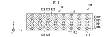
- FIG. 3 is an enlarged cross-sectional view of a part of the optical memory 10A.
- FIG. 3 is a cross-sectional view corresponding to the cross-sectional view taken along the line AA of the optical memory 10 shown in FIG.
- Each of the support 11A, the main surfaces 11A1, 11A2, and the nanoparticles 12A in the optical memory 10A corresponds to the support 11, the main surfaces 111, 112, and the nanoparticles 12 in the optical memory 10, respectively.
- a part of the plurality of nanoparticles 12 is embedded in the support 11, and the nanoparticles 12 are scattered in layers (two-dimensionally) in the plane of the main surface 111.
- the plurality of nanoparticles 12A are composed of the first nanoparticles 121, the second nanoparticles 122, the third nanoparticles 123, the fourth nanoparticles 124, and the fifth nanoparticles 125. Has been done.
- the first to fifth nanoparticles 121 to 125 are not distinguished, they are also referred to as the i-th nanoparticles 12i (i is an integer of 1 or more and 5 or less).
- Each of the i-th nanoparticles 12i is scattered in a layer like the nanoparticles 12 of the optical memory 10. However, each of the i-th nanoparticles 12i has a different scattered depth (distance from the main surface 11A1 in the thickness direction) as compared with the nanoparticles 12.
- the first nanoparticles 121 are provided in the vicinity of the main surface 11A1 in the inside of the support 11A.
- the second nanoparticles 122 are provided on the lower side (negative direction side of the z-axis) of the first nanoparticles 121 and at positions separated by a distance D12.
- the third nanoparticles 123 are provided on the lower side (negative direction side of the z-axis) of the second nanoparticles 122 and at positions separated by a distance D23.
- the fourth nanoparticles 124 are provided at positions below the third nanoparticles 123 (on the negative direction side of the z-axis) and separated by a distance D34.
- the fifth nanoparticles 125 are provided on the lower side (negative direction side of the z-axis) of the fourth nanoparticles 124 and at positions separated by a distance D34.
- each of the i-th nanoparticles 12i is laminated inside the support 11A.
- each of the i-th nanoparticles 12i is arranged on one axis along the thickness direction (see FIG. 3).
- the optical memory 10A when the first nanoparticles 121 to the fifth nanoparticles 125 arranged on one axis along the thickness direction are regarded as one nanoparticles group, a plurality of nanoparticles groups are formed. I have. The nanoparticles are separated from each other when the main surface 11A1 is viewed in a plan view from the normal direction. Therefore, the optical memory 10A is an example of an optical memory in which some of the plurality of nanoparticles 12A are arranged along the thickness direction. However, in one modification of the optical memory 10A, a configuration having only one nanoparticle group can be adopted. One modification of the optical memory 10A is an example of an optical memory in which all of the plurality of nanoparticles 12A are arranged along the thickness direction.
- the optical memory 10 shown in FIGS. 1 and 2 and the optical memory 10A shown in FIG. 3 include film forming technology represented by sputtering and vacuum vapor deposition, and microfabrication technology represented by photolithography and electron beam lithography. , Can be manufactured by combining.
- various methods that enable selective etching and selective deposition by FIB (Focused Ion Beam), and a technique called ALD (Atomic Layer Deposition) that can selectively add and deposit one atomic layer at a time are also suitable. It can be used.
- nanoparticles 12 and 12A for example, a hot injection technique used for manufacturing quantum dots, a nanoparticle manufacturing technique using a microreactor, silica, titanium oxide, and the like are formed.
- the sol-gel method used in the above can be diverted.
- the technique for producing nanoparticles 12 and 12A is not limited to this.
- a method may be used in which a desired phase change material layer is formed into a flat film by a method such as sputtering or vacuum vapor deposition, and then etched into nanoparticles by a method such as lithography.
- a self-assembly type nanostructure forming technique using a block copolymer can be used.
- this technique can be preferably used.
- a Subtractive molding method by combining a conventional photolithography technique and a self-assembly technique using a block copolymer can be used, or additive processing can be performed by combining an ALD or the like and a self-assembly technique. You can also.
- a desired pattern can be formed by scraping off unnecessary parts by etching using a fine pattern self-formed by the block copolymer as a mask.
- a desired shape can be formed by selectively adsorbing atoms only to one of the polymer chain components of the block copolymer using ALD or the like.
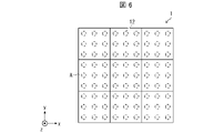
- FIG. 4 is a perspective view of the light diffraction element 1.
- FIG. 5 is an enlarged perspective view of a part (9 cells) of the optical diffraction element 1.
- FIG. 6 is an enlarged plan view of a part (9 cells) of the optical diffractive element 1, wherein the optical diffractive element 1 is mounted on the main surface of the support 11 (main surfaces 111 and 112 shown in FIG. 1). It is a plan view obtained when viewed in a plan view from a normal and an elaborate direction (z-axis direction).
- the substrate S constituting the optical diffraction element 1 is not shown.
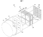
- the optical diffraction element 1 is a flat plate-shaped optical diffraction element, and in the first embodiment, a plurality of microcells A having thicknesses or refractive indexes set independently of each other, a base B, and the first embodiment. It is composed of the above-described optical memory 10 and the substrate S.
- Each microcell A is an example of a cell and is made of a translucent resin.
- the signal light transmitted through the microcells A interferes with each other, so that a predetermined optical calculation is performed.
- the intensity distribution of the signal light output from the optical diffraction element 1 represents the result of the optical signal.
- the "microcell” refers to, for example, a cell having a cell size of less than 10 ⁇ m.
- the "cell size” refers to the square root of the area of the cell. For example, when the plan view shape of the microcell is square, the cell size is the length of one side of the cell.
- the lower limit of the cell size is not particularly limited, but is, for example, 1 nm.
- the optical diffraction element 1 illustrated in FIG. 4 is composed of 2000 ⁇ 2000 microcells A arranged in a matrix.
- the plan view shape of each microcell A is, for example, a 1 ⁇ m ⁇ 1 ⁇ m square, and the plan view shape of the light diffraction element 1 is, for example, a 2 mm ⁇ 2 mm square.
- the cell size, the plan view shape of each microcell A, and the plan view shape of the light diffraction element 1 are not limited to the above examples, and can be appropriately determined.
- each microcell A is composed of a square columnar pillar having a square bottom surface whose side length is equal to the cell size.
- the amount of phase change of the light transmitted through the microcell A is determined according to the height of the pillar. That is, the amount of phase change of the light transmitted through the microcell A composed of the pillars having a high height becomes large, and the amount of the phase change of the light transmitted through the microcell A composed of the pillars having a low height becomes small.
- the base B is made of the same resin as each microcell A.
- the thickness of the base B is, for example, 100 ⁇ m, but is not limited thereto.
- FIG. 4 in order to make the configuration of the optical diffraction element 1 easy to understand, the base B and each microcell A are only shown separately in the optical diffraction element 1.
- the base B and each microcell A are manufactured as an optical diffraction element 1 integrated with the same resin. Therefore, in FIG. 5, the boundary between the base B and each microcell A is illustrated by a virtual line (dashed-dotted line) in the same manner as the boundary between adjacent microcells A.
- optical memory 10 shown in FIG. 4 has the same configuration as the optical memory 10 described with reference to FIGS. 1 and 2 in the first embodiment. Therefore, in the present embodiment, the same reference numerals are given to the optical memory 10 and each member constituting the optical memory 10, and the description thereof will be omitted. In the present embodiment, the optical memory 10 is interposed between the substrate S, which will be described later, and the base B of the optical diffraction element 1.
- the nine nanoparticles 12 which are a part of the plurality of nanoparticles 12 and which are a group of nine nanoparticles 12 in the in-plane direction of the main surface of the support 11 are in the optical memory 10. It constitutes one section (see FIG. 6). Then, each microcell A is assigned any one of the compartments composed of nine nanoparticles 12.
- the light diffractive element 1 When light having a spatial intensity distribution (that is, signal light) is incident, the light diffractive element 1 changes the spatial intensity distribution of the incident light into another spatial intensity distribution according to the thickness or refractive index of each microcell A. Output after conversion. According to the optical diffraction element 1, since each microcell A and each partition have a one-to-one correspondence, signal light having a spatial intensity distribution is used as light for writing, and the optical diffraction element 1 converts it. It is possible to record the spatial intensity distribution after this.
- the optical diffraction element 1 instead of using the signal light having a spatial intensity distribution as the light for writing, the light for writing different from the signal light is used to write something to each microcell A of the optical memory 10. May be done. By writing something to each microcell A of the optical memory 10, the amount of phase change of the light transmitted through each microcell A can be changed. Therefore, in the optical diffraction element 1, the optical memory 10 functions as a phase change amount variable mechanism for adjusting the phase change amount of the light transmitted through each microcell A after the fact.
- the substrate S is a plate-shaped member made of a translucent material.
- quartz glass is used as a translucent material.
- the material having translucency is not limited to quartz glass and can be appropriately selected.
- the optical memory 10, the base B, and the plurality of microcells A are laminated on one main surface of the substrate S in this order.
- the light diffraction element 1 adopts a transmission type configuration.
- the light diffraction element according to one aspect of the present invention is not limited to the transmission type and may be a reflection type.
- a substrate whose main surface is a mirror surface can be used instead of the substrate S made of a translucent material.
- a configuration may be adopted in which a substrate having a mirror surface as the main surface is superposed on the main surface on the side of the pair of main surfaces of the substrate S on which the optical memory 10 is not formed.
- the optical memory 10A shown in FIG. 3 can be used instead of the optical memory 10 shown in FIGS. 1 and 2.
- the optical memory 10A instead of the optical memory 10
- the spatial intensity distribution after the conversion by the optical diffraction element 1 can be recorded at multiple levels.
- the optical memory 10A may be used as the phase change amount variable mechanism.
- the fifth layer of nanoparticles 12i are arranged along the thickness direction of the support 11A. Therefore, the optical memory 10A can widen the adjustment range when changing the phase change amount of the light transmitted through each microcell A as compared with the optical memory 10. Therefore, according to this configuration, it is possible to provide the optical diffraction element 1 having a wider adjustment range of the amount of phase change in each microcell A.
- one optical diffraction element 1 has been described as having an optical memory 10.
- a plurality of stages of optical diffraction elements for example, optical diffraction elements 221 to 225
- the optical memory 10 in FIG. 7
- the optical memory 10B may be arranged further after the optical diffraction element (for example, the optical diffraction element 225) in the final stage.
- Each of the optical diffractive elements 221 to 225 acts in order on the signal light having the spatial intensity distribution, so that the multi-stage optical diffractive element functions as an optical arithmetic unit.
- the optical memory 10 is provided after the optical diffraction element 225, it is possible to record the optical calculation result by the optical diffraction elements 221 to 225.
- the plurality of stages of the optical diffraction element may be a transmission type or a reflection type.
- one optical diffraction element 1 includes an optical memory 10, and an optical arithmetic unit can be configured by stacking a plurality of such optical diffraction elements 1 in a plurality of stages.
- an optical arithmetic unit capable of ex post facto adjusting the calculation content. Can be done.
- the optical memory 10A instead of the optical memory 10
- the adjustment range in each optical diffraction element 221 to 225 can be further widened.
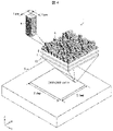
- FIG. 7 is a perspective view of the recording system 20.
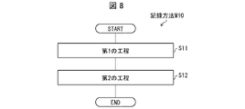
- FIG. 8 is a flowchart of the recording method M10 executed by the recording system 20.
- FIG. 9 is a schematic diagram illustrating the information recorded by the recording method M10.
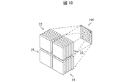
- FIG. 10 is a perspective view of the optical arithmetic units 22 to 24 and the optical memory 10C constituting the recording system 20C, which is a modification of the recording system 20.
- the recording system 20 includes a beam splitter 21, four optical arithmetic units 22 to 25, and an optical memory 10B.
- the beam splitter 21 is a tunnel type beam splitter having an entrance surface 211 and an exit surface 212.
- the exit surface 212 is provided with a first region 2121, a second region 2122, a third region 2123, and a fourth region 2124 on which still images having different shooting timings are formed. ..
- the beam splitter 21 includes a split projection unit and a delay generation unit.
- the divided projection unit divides and projects the moving image incident on the incident surface 211 onto a plurality of (four in the present embodiment) sub moving images. At this point, the four sub-moving images that are divided and projected are the same moving image.
- the beam splitter 21 may be, for example, a normal beam splitter followed by a mechanism such as a rotary optical chopper that can be time-lagged. Further, a special structure having both functions as used in a high-speed camera is also preferably used.
- the delay generation unit generates a still image frame by frame from each of the four sub-moving images while changing the shooting timing.
- each still image generated from each of the four sub moving images is, in order from the earliest shooting timing, the first still image, the second still image, the third still image, and the fourth. Called a still image.
- the delay generation unit forms an image of each of the first to fourth still images in the first to fourth regions 2121 to 2124, respectively.
- the difference in shooting timing between temporally adjacent still images is the same. Therefore, it exists between the first still image and the second still image, between the second still image and the third still image, and between the third still image and the fourth still image.
- the delay times are all the same.
- This delay time can be appropriately set according to the observation target, but in the present embodiment, it is appropriately set within a range of, for example, 10 n seconds or more and 2 ms or less. By setting the delay time within this range, each still image can be taken at a higher speed than the typical high-speed cameras on the market.
- optical calculation storage Each of the optical arithmetic units 22 to 25 is configured in the same manner. Therefore, here, the optical arithmetic unit 22 will be used for description.
- the optical arithmetic unit 22 is composed of five optical diffraction elements 221 to 225 (see FIG. 7).
- the optical diffractive element so that the region in which the microcell A, which is the effective region of each of the optical diffractive elements 221 to 225, is formed, exactly overlaps. 221 to 225 are laminated in this order.
- the light diffractive elements 221 to 225 stacked in this way function as an optical arithmetic unit by sequentially acting on signal light having a spatial intensity distribution.
- the optical arithmetic unit 22 uses the first still image formed in the first region 2121 as the signal light, and obtains the calculation result which is the result of the optical diffraction elements 221 to 225 acting on the signal light in order. Output to.
- each of the optical arithmetic devices 23 to 25 uses each of the second to fourth still images imaged in the second to fourth regions 2122 to 2124 as signal light, and 5 for each signal light.
- the calculation result which is the result of the light diffraction elements of the stage acting in order, is output to the subsequent stage.
- the optical memory 10B is an optical memory configured in the same manner as the optical memory 10 shown in FIGS. 1 and 2.
- the light receiving surface of the optical memory 10B is divided into first to fourth regions R1 to R4.
- Each of the first to fourth regions R1 to R4 is arranged so as to face the fifth stage optical diffraction element of the optical arithmetic units 22 to 25, respectively.
- the first region R1 records the result of optical arithmetic performed by the optical arithmetic unit 22 on the first still image.
- the second region R2 records the result of the calculation by the optical arithmetic unit 23 for the second still image
- the third region R3 is the optical arithmetic unit for the third still image.
- 24 records the result of the calculation
- the fourth region R4 records the result of the optical calculation device 25 performing the calculation on the fourth still image. Therefore, the optical memory 10B records the results of optical calculations performed by the optical arithmetic units 22 to 25 on the first to fourth still images in different first to fourth regions R1 to R4.
- each optical calculation device 22 to 25 performs optical calculation on a plurality of still images with a slight time difference due to the delay generation unit of the beam splitter 21.
- the optical calculation result can be recorded.
- the recording method M10 carried out by the recording system 20 includes a first step S11 and a second step S12.
- each of the first to fourth still images with a time difference due to the delay generation unit of the beam splitter 21 is incident on the first to fourth regions R1 to R4 of the optical memory 10B, respectively. It is a process.
- Each of the first to fourth still images is an example of a plurality of signal lights whose spatial intensity distribution represents specific information.
- the second step S12 is a step of writing the first to fourth still images to the optical memory 10B, using each of the first to fourth still images as light for writing.
- each of the first to fourth still images may be recorded in the first to fourth regions R1 to R4, which are different regions of the optical memory 10B. However, it may be recorded in the same area as in the optical memory 10C shown in FIG.
- the recording system 20 irradiates the entire surface of the optical memory 10B with a light source that emits light for reading and the light for reading in order to read the information recorded in the optical memory 10B. It includes a configured optical system and a photodetector that detects light after passing through the optical memory 10B.
- the light for reading is different from the first to fourth still images, which are signal lights for writing.
- the light for reading is emitted from the gap provided between the optical arithmetic units 22 to 25 and the optical memory 10B to the entire surface of the optical memory 10B using an optical system.
- the photodetector is an optical sensor array in which a plurality of optical sensors are arranged in a matrix so that the light transmitted through the nanoparticles 12 constituting the optical memory 10B can be detected.
- the control unit of the recording system 20 can acquire the spatial intensity distribution of light according to the light intensity signal output by the optical sensor array of the photodetector unit. Therefore, the control unit can read the information written in the optical memory 10B as the spatial intensity distribution of light.
- FIG. 9 is an example of information recorded by the recording method M10.
- the light intensity signal output by the optical sensor array of the photodetector unit is associated with the first to fourth regions R1 to R4 of the optical memory 10B.
- the lower left point in each of the first to fourth regions R1 to R4 is defined as the origin.
- the control unit determines whether or not any object OB is included in each of the first to fourth regions R1 to R4. When each of the first to fourth regions R1 to R4 includes some object OB, the control unit calculates the coordinates of the points P1 to P4 which are the centers of gravity of the object OB. The control unit can infer the locus of the object OB using the coordinates of the points P1 to P4.
- the recording system 20 configured in this way can predict the movement of an object (for example, a flying object) moving at high speed after detecting the presence of the object.
- an object for example, a flying object
- the recording system 20 is mounted on a moving object (for example, a drone)
- the moving object is moving at high speed and detects the presence of an object that may become an obstacle or collide. Then, the movement of the object can be predicted, and the movement of the object can be controlled based on the prediction result. Therefore, this moving body can avoid a collision with an object or the like.
- the optical memory according to the first aspect of the present invention is a plurality of nanoparticles composed of a support and a phase changing material that undergoes a phase change between a crystalline phase and an amorphous phase upon irradiation with light. It comprises a plurality of nanoparticles, which are supported by a support. In this optical memory, the nanoparticles are separated from each other in at least one of the in-plane direction of the specific surface and the normal direction of the specific surface.
- each nanoparticles separated from each other in at least one of the in-plane direction of the specific surface and the normal direction of the specific surface functions as a storage material. Since the storage material is composed of nanoparticles having a particle size of nano-order, the light power and / or energy required to realize the phase change in each nanoparticles is more than that of the bulk & plane type optical memory. Can also be suppressed. Therefore, this optical memory can improve the energy efficiency when changing the phase of each partition.
- the optical memory according to the second aspect of the present invention in addition to the configuration of the optical memory according to the first aspect described above, at least a part of each of the nanoparticles is embedded in the support.
- a configuration is adopted in which the thermal conductivity of the material constituting the support is lower than the thermal conductivity of the material constituting each of the nanoparticles.
- each nanoparticle can be reliably supported.
- a support made of a material having a low thermal conductivity is interposed around the nanoparticles, it is possible to suppress energy dissipation due to heat conduction from the nanoparticles. Therefore, the heat generated by each nanoparticles absorbing the laser beam for writing is less likely to escape to the surrounding support and other nanoparticles, so that energy efficiency can be further improved.
- optical memory according to the third aspect of the present invention in addition to the configuration of the optical memory according to the first aspect or the second aspect described above, some or all nanoparticles among the plurality of nanoparticles are obtained. Has adopted a configuration in which the particles are arranged along the normal direction of the specific surface.
- the number of nanoparticles whose phase changes can be controlled according to the power and / or energy of the laser beam. Since the phase-changed nanoparticles (for example, amorphous phase nanoparticles) have different light refractive index and absorption rate than the pre-phase-changed nanoparticles (for example, nanoparticles in the crystal layer), a laser for regeneration is used. The number of phase-changed nanoparticles can be detected using light. Therefore, according to this optical memory, a multi-level optical memory can be realized.
- each of the nanoparticles is in the in-plane direction. In, a configuration that is periodically arranged is adopted.
- each partition is periodically arranged inside the optical memory. Therefore, when the laser beam for writing has a spatial intensity distribution, the optical memory can record the spatial intensity distribution.
- the nanoparticles and the support are transparent.
- the configuration is adopted, which is composed of a material having light property.
- the writing light incident on the optical memory is emitted toward the rear stage of the optical memory. Therefore, the optical memory can be arranged in front of another optical element (for example, an optical diffraction element). Further, according to this configuration, when a plurality of nanoparticles are a multi-level optical memory arranged along the normal direction of a specific surface, it is possible to write to the nanoparticles provided at the last stage.
- the optical diffraction element according to the sixth aspect of the present invention is a plurality of cells in which the thickness or the refractive index are set independently of each other, and the optical memory according to any one of the above-mentioned first to fifth aspects. It is provided with an optical memory stacked in the plurality of cells.
- each of the regions obtained by projecting the bottom surface of each cell onto the specific surface is used as a partition of the optical memory, and each partition is one or a plurality of nanoparticles that are a part of the plurality of nanoparticles. Nanoparticles are arranged.
- the optical diffractive element converts the spatial intensity distribution of the incident light into another spatial intensity distribution according to the thickness or refractive index of each cell, and then outputs the light.
- the optical memory included in the optical diffraction element can increase the energy efficiency when changing the phase of each section, as in the optical memory according to the first aspect. Therefore, this optical diffractive element can increase the energy efficiency in recording the spatial intensity distribution after the optical diffractive element has been converted.
- the recording method according to the seventh aspect of the present invention is a plurality of nanoparticles composed of a phase changing material that undergoes a phase change between a crystalline phase and an amorphous phase by irradiation with light, and is in a specific plane.
- This is a recording method using an optical memory having a plurality of nanoparticles separated from each other in the direction.
- This recording method is a first step in which a plurality of signal lights whose spatial intensity distributions represent specific information, and a plurality of signal lights each having a time difference are incident on the optical memory, and light for writing each signal light.
- the second step of recording each signal light in the optical memory is included.
- each signal light is transmitted to a different region of the optical memory.
- the configuration to record is adopted.
- each signal light is recorded in a different area of the optical memory, it is easy to obtain specific information represented by each signal light as compared with the case where each signal light is recorded in the same area of the optical memory. It can be read.
- Optical diffractive element A Microcell B Base S Substrate 10, 10A, 10B Optical memory R1 to R4 First to fourth regions 11, 11A Support 111, 11A1 Main surface (specific surface) 112,11A2 Main surface 12,12A Nanoparticles 121-125 First to fifth nanoparticles 20 Recording system
Landscapes
- Physics & Mathematics (AREA)
- Optics & Photonics (AREA)
- Chemical & Material Sciences (AREA)
- Crystallography & Structural Chemistry (AREA)
- General Physics & Mathematics (AREA)
- Inorganic Chemistry (AREA)
- Optical Recording Or Reproduction (AREA)
- Optical Head (AREA)
Priority Applications (2)
| Application Number | Priority Date | Filing Date | Title |
|---|---|---|---|
| US18/265,304 US12142307B2 (en) | 2020-12-28 | 2021-08-20 | Optical memory, optical diffraction element, and recording method |
| JP2022572902A JP7492037B2 (ja) | 2020-12-28 | 2021-08-20 | 光メモリ、光回折素子、及び、記録方法 |
Applications Claiming Priority (2)
| Application Number | Priority Date | Filing Date | Title |
|---|---|---|---|
| JP2020219578 | 2020-12-28 | ||
| JP2020-219578 | 2020-12-28 |
Publications (1)
| Publication Number | Publication Date |
|---|---|
| WO2022145084A1 true WO2022145084A1 (ja) | 2022-07-07 |
Family
ID=82259234
Family Applications (1)
| Application Number | Title | Priority Date | Filing Date |
|---|---|---|---|
| PCT/JP2021/030685 Ceased WO2022145084A1 (ja) | 2020-12-28 | 2021-08-20 | 光メモリ、光回折素子、及び、記録方法 |
Country Status (3)
| Country | Link |
|---|---|
| US (1) | US12142307B2 (enExample) |
| JP (1) | JP7492037B2 (enExample) |
| WO (1) | WO2022145084A1 (enExample) |
Families Citing this family (1)
| Publication number | Priority date | Publication date | Assignee | Title |
|---|---|---|---|---|
| JP7492037B2 (ja) * | 2020-12-28 | 2024-05-28 | 株式会社フジクラ | 光メモリ、光回折素子、及び、記録方法 |
Citations (6)
| Publication number | Priority date | Publication date | Assignee | Title |
|---|---|---|---|---|
| JP2005285162A (ja) * | 2004-03-26 | 2005-10-13 | Ricoh Co Ltd | 光記録情報記録媒体 |
| JP3793040B2 (ja) * | 2001-05-09 | 2006-07-05 | 株式会社東芝 | 記録媒体およびその製造方法 |
| JP2010531995A (ja) * | 2007-06-26 | 2010-09-30 | ヒューレット−パッカード デベロップメント カンパニー エル.ピー. | 電界強化構造、及び該構造を利用した検出装置 |
| WO2011010447A1 (ja) * | 2009-07-21 | 2011-01-27 | パナソニック株式会社 | 情報記録媒体、光学情報記録再生装置、光学情報記録再生方法及び情報記録媒体の製造方法 |
| WO2013014935A1 (ja) * | 2011-07-27 | 2013-01-31 | パナソニック株式会社 | 記録媒体、光情報装置及び記録媒体の製造方法 |
| JP2013125259A (ja) * | 2011-12-16 | 2013-06-24 | Canon Inc | 回折光学素子、光学系および光学機器 |
Family Cites Families (7)
| Publication number | Priority date | Publication date | Assignee | Title |
|---|---|---|---|---|
| US6387530B1 (en) * | 1999-08-27 | 2002-05-14 | Seagate Technology Llc | Patterned magnetic media via thermally induced phase transition |
| JP2001325745A (ja) | 2000-05-16 | 2001-11-22 | Sony Corp | 光学記録媒体と、その再生装置および記録再生装置 |
| JP2001347756A (ja) * | 2000-06-06 | 2001-12-18 | Fuji Photo Film Co Ltd | 光記録媒体とこれを用いた光記録方法 |
| KR20060064647A (ko) * | 2003-08-20 | 2006-06-13 | 코닌클리케 필립스 일렉트로닉스 엔.브이. | 광 기록매체 |
| US8422197B2 (en) * | 2009-07-15 | 2013-04-16 | Applied Nanotech Holdings, Inc. | Applying optical energy to nanoparticles to produce a specified nanostructure |
| US20110297358A1 (en) * | 2010-06-07 | 2011-12-08 | The Boeing Company | Nano-coating thermal barrier and method for making the same |
| JP7492037B2 (ja) * | 2020-12-28 | 2024-05-28 | 株式会社フジクラ | 光メモリ、光回折素子、及び、記録方法 |
-
2021
- 2021-08-20 JP JP2022572902A patent/JP7492037B2/ja active Active
- 2021-08-20 WO PCT/JP2021/030685 patent/WO2022145084A1/ja not_active Ceased
- 2021-08-20 US US18/265,304 patent/US12142307B2/en active Active
Patent Citations (6)
| Publication number | Priority date | Publication date | Assignee | Title |
|---|---|---|---|---|
| JP3793040B2 (ja) * | 2001-05-09 | 2006-07-05 | 株式会社東芝 | 記録媒体およびその製造方法 |
| JP2005285162A (ja) * | 2004-03-26 | 2005-10-13 | Ricoh Co Ltd | 光記録情報記録媒体 |
| JP2010531995A (ja) * | 2007-06-26 | 2010-09-30 | ヒューレット−パッカード デベロップメント カンパニー エル.ピー. | 電界強化構造、及び該構造を利用した検出装置 |
| WO2011010447A1 (ja) * | 2009-07-21 | 2011-01-27 | パナソニック株式会社 | 情報記録媒体、光学情報記録再生装置、光学情報記録再生方法及び情報記録媒体の製造方法 |
| WO2013014935A1 (ja) * | 2011-07-27 | 2013-01-31 | パナソニック株式会社 | 記録媒体、光情報装置及び記録媒体の製造方法 |
| JP2013125259A (ja) * | 2011-12-16 | 2013-06-24 | Canon Inc | 回折光学素子、光学系および光学機器 |
Also Published As
| Publication number | Publication date |
|---|---|
| JPWO2022145084A1 (enExample) | 2022-07-07 |
| US12142307B2 (en) | 2024-11-12 |
| JP7492037B2 (ja) | 2024-05-28 |
| US20240038264A1 (en) | 2024-02-01 |
Similar Documents
| Publication | Publication Date | Title |
|---|---|---|
| US8663772B2 (en) | Minute structure and information recording medium | |
| JP4607139B2 (ja) | 追記型情報記録媒体及びマスター基板 | |
| TWI425506B (zh) | 用於製造母版之方法及用於製造光碟之方法 | |
| TW200415642A (en) | Optical recording medium and method for manufacturing the same | |
| JP7492037B2 (ja) | 光メモリ、光回折素子、及び、記録方法 | |
| EP1494229A1 (en) | Information recording medium and its production method, and optical information recording/reproducing apparatus | |
| EP1553577A1 (en) | Information recording medium, process for producing the same and optical information recording and reproducing device | |
| JP2008290227A (ja) | 微小構造体 | |
| JP2010170691A (ja) | 情報記録媒体及びその記録/再生装置 | |
| Yamada et al. | Phase‐Change Nanodot Material for an Optical Memory | |
| US8295141B2 (en) | Pattern and method for forming the same | |
| TWI311748B (en) | Optical information recording medium, method for producing the medium, and method and apparatus for recording information using the medium | |
| CN100509222C (zh) | 构造体及其制造方法、形成用媒体,光记录媒体及其再现方法 | |
| JP2000260060A (ja) | 光情報記録媒体 | |
| US20100008202A1 (en) | Optical information recording medium, recording particle, method for reproducing optical information, optical information reproducing apparatus, method for recording optical information, and optical information recording apparatus | |
| JP4000365B2 (ja) | 平板型レンズを用いた結像方法及び該結像方法を利用した高密度光記録方法 | |
| JP2004241088A (ja) | 光記録再生方法、光記録再生装置、及び光記録媒体 | |
| US20130337217A1 (en) | Information recording medium and manufacturing method of same | |
| Shintani et al. | Sub-terabyte-data-capacity optical discs realized by three-dimensional pit selection | |
| Lee et al. | High-resolution mastering using AlNiGd metallic glass thin film as thermal absorption layer | |
| Ahluwalia | Data storage devices | |
| WO2007043359A1 (ja) | 超解像光記録媒体及び超解像光記録媒体への情報記録方法 | |
| JP4134110B2 (ja) | 光記録媒体 | |
| JP2007122789A (ja) | 多層光記録媒体 | |
| JP2008257863A (ja) | 光情報記録媒体、その再生方法及びその製造方法 |
Legal Events
| Date | Code | Title | Description |
|---|---|---|---|
| 121 | Ep: the epo has been informed by wipo that ep was designated in this application |
Ref document number: 21914945 Country of ref document: EP Kind code of ref document: A1 |
|
| ENP | Entry into the national phase |
Ref document number: 2022572902 Country of ref document: JP Kind code of ref document: A |
|
| WWE | Wipo information: entry into national phase |
Ref document number: 18265304 Country of ref document: US |
|
| NENP | Non-entry into the national phase |
Ref country code: DE |
|
| 122 | Ep: pct application non-entry in european phase |
Ref document number: 21914945 Country of ref document: EP Kind code of ref document: A1 |