WO2022138733A1 - Dispositif électroluminescent - Google Patents
Dispositif électroluminescent Download PDFInfo
- Publication number
- WO2022138733A1 WO2022138733A1 PCT/JP2021/047608 JP2021047608W WO2022138733A1 WO 2022138733 A1 WO2022138733 A1 WO 2022138733A1 JP 2021047608 W JP2021047608 W JP 2021047608W WO 2022138733 A1 WO2022138733 A1 WO 2022138733A1
- Authority
- WO
- WIPO (PCT)
- Prior art keywords
- light
- light emitting
- emitting element
- reflecting surface
- light reflecting
- Prior art date
Links
- 230000003287 optical effect Effects 0.000 claims abstract description 55
- 238000006243 chemical reaction Methods 0.000 claims description 86
- 230000001681 protective effect Effects 0.000 claims description 7
- 238000013459 approach Methods 0.000 claims description 3
- 238000007789 sealing Methods 0.000 description 35
- 239000000463 material Substances 0.000 description 31
- 229910052751 metal Inorganic materials 0.000 description 29
- 239000002184 metal Substances 0.000 description 29
- 238000009826 distribution Methods 0.000 description 15
- 239000000919 ceramic Substances 0.000 description 14
- 239000004065 semiconductor Substances 0.000 description 12
- 238000000605 extraction Methods 0.000 description 8
- 238000005245 sintering Methods 0.000 description 7
- OAICVXFJPJFONN-UHFFFAOYSA-N Phosphorus Chemical compound [P] OAICVXFJPJFONN-UHFFFAOYSA-N 0.000 description 6
- 239000010931 gold Substances 0.000 description 5
- TWNQGVIAIRXVLR-UHFFFAOYSA-N oxo(oxoalumanyloxy)alumane Chemical compound O=[Al]O[Al]=O TWNQGVIAIRXVLR-UHFFFAOYSA-N 0.000 description 5
- 229920005989 resin Polymers 0.000 description 5
- 239000011347 resin Substances 0.000 description 5
- JNDMLEXHDPKVFC-UHFFFAOYSA-N aluminum;oxygen(2-);yttrium(3+) Chemical compound [O-2].[O-2].[O-2].[Al+3].[Y+3] JNDMLEXHDPKVFC-UHFFFAOYSA-N 0.000 description 4
- PMHQVHHXPFUNSP-UHFFFAOYSA-M copper(1+);methylsulfanylmethane;bromide Chemical compound Br[Cu].CSC PMHQVHHXPFUNSP-UHFFFAOYSA-M 0.000 description 4
- 238000009792 diffusion process Methods 0.000 description 4
- VYPSYNLAJGMNEJ-UHFFFAOYSA-N silicon dioxide Inorganic materials O=[Si]=O VYPSYNLAJGMNEJ-UHFFFAOYSA-N 0.000 description 4
- 239000000126 substance Substances 0.000 description 4
- 229910019901 yttrium aluminum garnet Inorganic materials 0.000 description 4
- 229910004298 SiO 2 Inorganic materials 0.000 description 3
- 229910052782 aluminium Inorganic materials 0.000 description 3
- 230000000694 effects Effects 0.000 description 3
- 239000011521 glass Substances 0.000 description 3
- 229910052737 gold Inorganic materials 0.000 description 3
- 238000012986 modification Methods 0.000 description 3
- 230000004048 modification Effects 0.000 description 3
- 230000002093 peripheral effect Effects 0.000 description 3
- 229910052594 sapphire Inorganic materials 0.000 description 3
- 239000010980 sapphire Substances 0.000 description 3
- HBMJWWWQQXIZIP-UHFFFAOYSA-N silicon carbide Chemical compound [Si+]#[C-] HBMJWWWQQXIZIP-UHFFFAOYSA-N 0.000 description 3
- 229910010271 silicon carbide Inorganic materials 0.000 description 3
- 229910052684 Cerium Inorganic materials 0.000 description 2
- 230000001154 acute effect Effects 0.000 description 2
- XAGFODPZIPBFFR-UHFFFAOYSA-N aluminium Chemical compound [Al] XAGFODPZIPBFFR-UHFFFAOYSA-N 0.000 description 2
- -1 and for example Substances 0.000 description 2
- GWXLDORMOJMVQZ-UHFFFAOYSA-N cerium Chemical compound [Ce] GWXLDORMOJMVQZ-UHFFFAOYSA-N 0.000 description 2
- 230000005284 excitation Effects 0.000 description 2
- 239000000945 filler Substances 0.000 description 2
- 230000017525 heat dissipation Effects 0.000 description 2
- CPLXHLVBOLITMK-UHFFFAOYSA-N magnesium oxide Inorganic materials [Mg]=O CPLXHLVBOLITMK-UHFFFAOYSA-N 0.000 description 2
- 239000000395 magnesium oxide Substances 0.000 description 2
- AXZKOIWUVFPNLO-UHFFFAOYSA-N magnesium;oxygen(2-) Chemical compound [O-2].[Mg+2] AXZKOIWUVFPNLO-UHFFFAOYSA-N 0.000 description 2
- 239000007769 metal material Substances 0.000 description 2
- 150000004767 nitrides Chemical class 0.000 description 2
- SIWVEOZUMHYXCS-UHFFFAOYSA-N oxo(oxoyttriooxy)yttrium Chemical compound O=[Y]O[Y]=O SIWVEOZUMHYXCS-UHFFFAOYSA-N 0.000 description 2
- RVTZCBVAJQQJTK-UHFFFAOYSA-N oxygen(2-);zirconium(4+) Chemical compound [O-2].[O-2].[Zr+4] RVTZCBVAJQQJTK-UHFFFAOYSA-N 0.000 description 2
- 238000012545 processing Methods 0.000 description 2
- 239000010453 quartz Substances 0.000 description 2
- 229910052814 silicon oxide Inorganic materials 0.000 description 2
- 229910052709 silver Inorganic materials 0.000 description 2
- 229910001928 zirconium oxide Inorganic materials 0.000 description 2
- 239000004925 Acrylic resin Substances 0.000 description 1
- 229910002704 AlGaN Inorganic materials 0.000 description 1
- 229910015363 Au—Sn Inorganic materials 0.000 description 1
- RYGMFSIKBFXOCR-UHFFFAOYSA-N Copper Chemical compound [Cu] RYGMFSIKBFXOCR-UHFFFAOYSA-N 0.000 description 1
- 229910052693 Europium Inorganic materials 0.000 description 1
- BPQQTUXANYXVAA-UHFFFAOYSA-N Orthosilicate Chemical compound [O-][Si]([O-])([O-])[O-] BPQQTUXANYXVAA-UHFFFAOYSA-N 0.000 description 1
- 229910052581 Si3N4 Inorganic materials 0.000 description 1
- 229910004283 SiO 4 Inorganic materials 0.000 description 1
- BQCADISMDOOEFD-UHFFFAOYSA-N Silver Chemical compound [Ag] BQCADISMDOOEFD-UHFFFAOYSA-N 0.000 description 1
- 229910010413 TiO 2 Inorganic materials 0.000 description 1
- 239000011358 absorbing material Substances 0.000 description 1
- 230000000903 blocking effect Effects 0.000 description 1
- 238000009529 body temperature measurement Methods 0.000 description 1
- 239000005388 borosilicate glass Substances 0.000 description 1
- 239000006229 carbon black Substances 0.000 description 1
- 239000002131 composite material Substances 0.000 description 1
- 239000004020 conductor Substances 0.000 description 1
- 229910052802 copper Inorganic materials 0.000 description 1
- 239000010949 copper Substances 0.000 description 1
- 239000013078 crystal Substances 0.000 description 1
- 238000013461 design Methods 0.000 description 1
- 238000010586 diagram Methods 0.000 description 1
- 239000003822 epoxy resin Substances 0.000 description 1
- OGPBJKLSAFTDLK-UHFFFAOYSA-N europium atom Chemical compound [Eu] OGPBJKLSAFTDLK-UHFFFAOYSA-N 0.000 description 1
- 239000002223 garnet Substances 0.000 description 1
- PCHJSUWPFVWCPO-UHFFFAOYSA-N gold Chemical compound [Au] PCHJSUWPFVWCPO-UHFFFAOYSA-N 0.000 description 1
- 238000010438 heat treatment Methods 0.000 description 1
- 239000003779 heat-resistant material Substances 0.000 description 1
- 229910010272 inorganic material Inorganic materials 0.000 description 1
- 239000011147 inorganic material Substances 0.000 description 1
- 238000005304 joining Methods 0.000 description 1
- 238000004519 manufacturing process Methods 0.000 description 1
- 238000002844 melting Methods 0.000 description 1
- 230000008018 melting Effects 0.000 description 1
- 238000000034 method Methods 0.000 description 1
- 229910052759 nickel Inorganic materials 0.000 description 1
- 239000002245 particle Substances 0.000 description 1
- 239000005011 phenolic resin Substances 0.000 description 1
- 239000000049 pigment Substances 0.000 description 1
- 229910052697 platinum Inorganic materials 0.000 description 1
- 229920000647 polyepoxide Polymers 0.000 description 1
- 239000000843 powder Substances 0.000 description 1
- 230000000630 rising effect Effects 0.000 description 1
- HQVNEWCFYHHQES-UHFFFAOYSA-N silicon nitride Chemical compound N12[Si]34N5[Si]62N3[Si]51N64 HQVNEWCFYHHQES-UHFFFAOYSA-N 0.000 description 1
- 229920002050 silicone resin Polymers 0.000 description 1
- 239000004332 silver Substances 0.000 description 1
- 238000006467 substitution reaction Methods 0.000 description 1
- 229910052715 tantalum Inorganic materials 0.000 description 1
- 229920002803 thermoplastic polyurethane Polymers 0.000 description 1
- 229920001187 thermosetting polymer Polymers 0.000 description 1
- 229910052719 titanium Inorganic materials 0.000 description 1
- 238000002834 transmittance Methods 0.000 description 1
Images


Classifications
-
- H—ELECTRICITY
- H01—ELECTRIC ELEMENTS
- H01L—SEMICONDUCTOR DEVICES NOT COVERED BY CLASS H10
- H01L33/00—Semiconductor devices having potential barriers specially adapted for light emission; Processes or apparatus specially adapted for the manufacture or treatment thereof or of parts thereof; Details thereof
- H01L33/48—Semiconductor devices having potential barriers specially adapted for light emission; Processes or apparatus specially adapted for the manufacture or treatment thereof or of parts thereof; Details thereof characterised by the semiconductor body packages
- H01L33/58—Optical field-shaping elements
- H01L33/60—Reflective elements
-
- F—MECHANICAL ENGINEERING; LIGHTING; HEATING; WEAPONS; BLASTING
- F21—LIGHTING
- F21V—FUNCTIONAL FEATURES OR DETAILS OF LIGHTING DEVICES OR SYSTEMS THEREOF; STRUCTURAL COMBINATIONS OF LIGHTING DEVICES WITH OTHER ARTICLES, NOT OTHERWISE PROVIDED FOR
- F21V7/00—Reflectors for light sources
- F21V7/04—Optical design
-
- F—MECHANICAL ENGINEERING; LIGHTING; HEATING; WEAPONS; BLASTING
- F21—LIGHTING
- F21S—NON-PORTABLE LIGHTING DEVICES; SYSTEMS THEREOF; VEHICLE LIGHTING DEVICES SPECIALLY ADAPTED FOR VEHICLE EXTERIORS
- F21S41/00—Illuminating devices specially adapted for vehicle exteriors, e.g. headlamps
- F21S41/10—Illuminating devices specially adapted for vehicle exteriors, e.g. headlamps characterised by the light source
- F21S41/14—Illuminating devices specially adapted for vehicle exteriors, e.g. headlamps characterised by the light source characterised by the type of light source
- F21S41/16—Laser light sources
-
- F—MECHANICAL ENGINEERING; LIGHTING; HEATING; WEAPONS; BLASTING
- F21—LIGHTING
- F21V—FUNCTIONAL FEATURES OR DETAILS OF LIGHTING DEVICES OR SYSTEMS THEREOF; STRUCTURAL COMBINATIONS OF LIGHTING DEVICES WITH OTHER ARTICLES, NOT OTHERWISE PROVIDED FOR
- F21V9/00—Elements for modifying spectral properties, polarisation or intensity of the light emitted, e.g. filters
- F21V9/30—Elements containing photoluminescent material distinct from or spaced from the light source
-
- H—ELECTRICITY
- H01—ELECTRIC ELEMENTS
- H01L—SEMICONDUCTOR DEVICES NOT COVERED BY CLASS H10
- H01L25/00—Assemblies consisting of a plurality of individual semiconductor or other solid state devices ; Multistep manufacturing processes thereof
- H01L25/03—Assemblies consisting of a plurality of individual semiconductor or other solid state devices ; Multistep manufacturing processes thereof all the devices being of a type provided for in the same subgroup of groups H01L27/00 - H01L33/00, or in a single subclass of H10K, H10N, e.g. assemblies of rectifier diodes
- H01L25/04—Assemblies consisting of a plurality of individual semiconductor or other solid state devices ; Multistep manufacturing processes thereof all the devices being of a type provided for in the same subgroup of groups H01L27/00 - H01L33/00, or in a single subclass of H10K, H10N, e.g. assemblies of rectifier diodes the devices not having separate containers
- H01L25/075—Assemblies consisting of a plurality of individual semiconductor or other solid state devices ; Multistep manufacturing processes thereof all the devices being of a type provided for in the same subgroup of groups H01L27/00 - H01L33/00, or in a single subclass of H10K, H10N, e.g. assemblies of rectifier diodes the devices not having separate containers the devices being of a type provided for in group H01L33/00
- H01L25/0753—Assemblies consisting of a plurality of individual semiconductor or other solid state devices ; Multistep manufacturing processes thereof all the devices being of a type provided for in the same subgroup of groups H01L27/00 - H01L33/00, or in a single subclass of H10K, H10N, e.g. assemblies of rectifier diodes the devices not having separate containers the devices being of a type provided for in group H01L33/00 the devices being arranged next to each other
-
- H—ELECTRICITY
- H01—ELECTRIC ELEMENTS
- H01S—DEVICES USING THE PROCESS OF LIGHT AMPLIFICATION BY STIMULATED EMISSION OF RADIATION [LASER] TO AMPLIFY OR GENERATE LIGHT; DEVICES USING STIMULATED EMISSION OF ELECTROMAGNETIC RADIATION IN WAVE RANGES OTHER THAN OPTICAL
- H01S5/00—Semiconductor lasers
- H01S5/02—Structural details or components not essential to laser action
- H01S5/022—Mountings; Housings
- H01S5/0225—Out-coupling of light
- H01S5/02255—Out-coupling of light using beam deflecting elements
-
- H—ELECTRICITY
- H01—ELECTRIC ELEMENTS
- H01S—DEVICES USING THE PROCESS OF LIGHT AMPLIFICATION BY STIMULATED EMISSION OF RADIATION [LASER] TO AMPLIFY OR GENERATE LIGHT; DEVICES USING STIMULATED EMISSION OF ELECTROMAGNETIC RADIATION IN WAVE RANGES OTHER THAN OPTICAL
- H01S5/00—Semiconductor lasers
- H01S5/02—Structural details or components not essential to laser action
- H01S5/022—Mountings; Housings
- H01S5/0225—Out-coupling of light
- H01S5/02257—Out-coupling of light using windows, e.g. specially adapted for back-reflecting light to a detector inside the housing
-
- H—ELECTRICITY
- H01—ELECTRIC ELEMENTS
- H01S—DEVICES USING THE PROCESS OF LIGHT AMPLIFICATION BY STIMULATED EMISSION OF RADIATION [LASER] TO AMPLIFY OR GENERATE LIGHT; DEVICES USING STIMULATED EMISSION OF ELECTROMAGNETIC RADIATION IN WAVE RANGES OTHER THAN OPTICAL
- H01S5/00—Semiconductor lasers
- H01S5/40—Arrangement of two or more semiconductor lasers, not provided for in groups H01S5/02 - H01S5/30
-
- F—MECHANICAL ENGINEERING; LIGHTING; HEATING; WEAPONS; BLASTING
- F21—LIGHTING
- F21S—NON-PORTABLE LIGHTING DEVICES; SYSTEMS THEREOF; VEHICLE LIGHTING DEVICES SPECIALLY ADAPTED FOR VEHICLE EXTERIORS
- F21S41/00—Illuminating devices specially adapted for vehicle exteriors, e.g. headlamps
- F21S41/10—Illuminating devices specially adapted for vehicle exteriors, e.g. headlamps characterised by the light source
- F21S41/19—Attachment of light sources or lamp holders
- F21S41/192—Details of lamp holders, terminals or connectors
-
- F—MECHANICAL ENGINEERING; LIGHTING; HEATING; WEAPONS; BLASTING
- F21—LIGHTING
- F21Y—INDEXING SCHEME ASSOCIATED WITH SUBCLASSES F21K, F21L, F21S and F21V, RELATING TO THE FORM OR THE KIND OF THE LIGHT SOURCES OR OF THE COLOUR OF THE LIGHT EMITTED
- F21Y2113/00—Combination of light sources
-
- H—ELECTRICITY
- H01—ELECTRIC ELEMENTS
- H01L—SEMICONDUCTOR DEVICES NOT COVERED BY CLASS H10
- H01L33/00—Semiconductor devices having potential barriers specially adapted for light emission; Processes or apparatus specially adapted for the manufacture or treatment thereof or of parts thereof; Details thereof
- H01L33/48—Semiconductor devices having potential barriers specially adapted for light emission; Processes or apparatus specially adapted for the manufacture or treatment thereof or of parts thereof; Details thereof characterised by the semiconductor body packages
- H01L33/50—Wavelength conversion elements
- H01L33/507—Wavelength conversion elements the elements being in intimate contact with parts other than the semiconductor body or integrated with parts other than the semiconductor body
Definitions
- This disclosure relates to a light emitting device.
- Patent Document 1 discloses a light source device that raises light emitted from a plurality of light emitting elements, reflects it by a reflecting surface of a mirror, and emits it to the outside.
- a plurality of light emitting elements are juxtaposed on the same side with respect to the rising mirror.
- Each light emitting element is considered to be a heat source. Therefore, if a plurality of light emitting elements are arranged close to each other, the heat sources come close to each other. Depending on the temperature characteristics of the light emitting element and the required light output, it may be preferable that the heat sources are separated from each other.
- the light emitting device is on a base having a mounting surface, a first light emitting element arranged on the mounting surface and emitting light passing through the first optical axis, and the mounting surface.
- a second light emitting element that is arranged and emits light that passes through the second optical axis
- a third light emitting element that is arranged on the mounting surface and emits light that passes through the third optical axis, and the first optical axis.
- a first light reflecting surface including a first position where light passing through is irradiated and inclined with respect to the mounting surface, and a second position including a second position where light passing through the second optical axis is irradiated and inclined with respect to the mounting surface.
- One or more light reflecting members including a second light reflecting surface and a third light reflecting surface including a third position where light passing through the third optical axis is irradiated and inclined with respect to the mounting surface.
- the first light emitting element has when the mounting surface is divided into a first region and a second region with a virtual first straight line passing through the second position and the third position as a boundary in a top view.
- the second light emitting element and the third light emitting element are arranged in the first region, and the second light emitting element and the third light emitting element are arranged in the second region, and the second light reflecting surface and the third light reflecting surface are the first 1 Arranged across a light reflecting surface.
- a light emitting device in which the arrangement of a plurality of light emitting elements serving as heat sources is dispersed.
- FIG. 3 is a cross-sectional view taken along the line II-II of FIG. 1 illustrating a light emitting device according to the present embodiment. It is a perspective view for demonstrating the internal structure of the light emitting device which concerns on this embodiment. It is a perspective view of the state which removed the wavelength conversion member and the sealing member from the light emitting device which concerns on this embodiment. It is a top view of the state which removed the wavelength conversion member and the sealing member from the light emitting device which concerns on this embodiment. It is a partially enlarged top view (No. 1) of the state which removed the wavelength conversion member and the sealing member from the light emitting device which concerns on this embodiment.
- FIG. 1 is a partially enlarged top view
- FIG. 2 is a partially enlarged top view (No. 2) in a state where the wavelength conversion member and the sealing member are removed from the light emitting device according to the present embodiment.
- FIG. 3 is a partially enlarged top view (No. 3) in a state where the wavelength conversion member and the sealing member are removed from the light emitting device according to the present embodiment.
- It is an image which shows the intensity distribution of the light incident on the 1st light reflection surface of the light emitting apparatus which concerns on this embodiment.
- It is an image which shows the intensity distribution of the light incident on the 2nd light reflection surface of the light emitting apparatus which concerns on this embodiment.
- It is a figure explaining the modification of the light reflection surface.
- a polygon such as a triangle or a quadrangle shall be referred to as a polygon including a shape in which the corners of the polygon are rounded, chamfered, chamfered, rounded, or the like. .. Further, not only the corner (edge of the side) but also the shape in which the middle part of the side is processed is also referred to as a polygon. That is, a shape that has been partially processed while leaving the polygon as a base is included in the interpretation of the "polygon" described in the present disclosure.
- the embodiments shown below exemplify a light emitting device or the like for embodying the technical idea of the present invention, and do not limit the present invention to the following.
- the dimensions, materials, shapes, relative arrangements, etc. of the components described below are not intended to limit the scope of the present invention to the specific description, but are exemplified. It was intended.
- the contents described in one embodiment can be applied to other embodiments and modifications.
- the size and positional relationship of the members shown in the drawings may be exaggerated in order to clarify the explanation. Further, in order to avoid the drawing from becoming excessively complicated, a schematic view in which some elements are not shown may be used, or an end view showing only the cut surface may be used as the cross-sectional view.
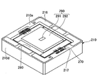
- FIG. 1 is a perspective view illustrating the light emitting device according to the present embodiment.
- FIG. 2 is a cross-sectional view taken along the line II-II of FIG. 1 illustrating the light emitting device according to the present embodiment.
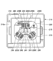
- FIG. 3 is a perspective view for explaining the internal structure of the light emitting device according to the present embodiment.
- FIG. 4 is a perspective view showing a state in which the wavelength conversion member and the sealing member are removed from the light emitting device according to the present embodiment.
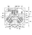
- FIG. 5 is a top view of the light emitting device according to the present embodiment in a state where the wavelength conversion member and the sealing member are removed. In FIG. 4, the wiring 270 is not shown.
- the light emitting device 200 includes a plurality of components.
- the plurality of components include a base 210, a first light emitting element 220A, a second light emitting element 220B, a third light emitting element 220C, one or more submounts 230, and one or more light reflecting members.
- a protection element 250, a temperature measuring element 260, a wiring 270, a sealing member 280, a wavelength conversion member 290, and a light shielding member 300 are included.
- the light emitting device 200 does not have to have all of these components.
- a plurality of configurations including at least a base 210, a first light emitting element 220A, a second light emitting element 220B, a third light emitting element 220C, and one or more light reflecting members having three light reflecting surfaces.
- a light emitting device 200 having an element can be realized.
- the illustrated light emitting device 200 includes a base 210, a first light emitting element 220A, a second light emitting element 220B, a third light emitting element 220C, and a sub corresponding to each light emitting element.
- a plurality of light reflecting members including a mount 230, a first light reflecting member 240A, a second light reflecting member 240B, and a third light reflecting member 240C, a protective element 250, a temperature measuring element 260, a wiring 270, and the like. It has a sealing member 280, a wavelength conversion member 290, and a light shielding member 300.
- the base 210 has an upper surface 210a, a lower surface 210b, one or more inner side surfaces 210c, one or more outer side surfaces 210d, and a bottom surface 210e.
- the bottom surface 210e is a mounting surface on which other components are arranged.
- the base 210 has a concave shape recessed in the direction from the upper surface 210a to the lower surface 210b. Further, the base portion 210 has a rectangular outer shape when viewed from above, and a recess is formed inside the outer outer shape.
- a frame is formed by one or a plurality of inner side surfaces 210c intersecting the upper surface 210a. That is, the base 210 includes a bottom surface 210e and a frame forming an inner side surface 210c extending above the bottom surface 210e. The recess of the base 210 is surrounded by the bottom surface 210e and this frame.
- top view refers to viewing the object from the normal direction of the top surface 210a of the base 210.
- shape of the upper surface 210a of the base 210 when the object is viewed from the normal direction may be referred to as a planar shape.
- the base 210 has one or more stepped portions 212 inside the frame.
- the step portion 212 is composed of only the upper surface and the side surface that intersects the upper surface and advances downward.
- the one or more inner side surfaces 210c include a side surface that intersects the upper surface 210a of the base portion 210 and a side surface of the step portion 212.
- the base 210 can be formed, for example, using ceramics as a main material.
- ceramics aluminum nitride, silicon nitride, aluminum oxide, or silicon carbide can be used as the ceramics.
- the base 210 is not limited to ceramics, and may be formed by using another material having an insulating property as a main material.
- One or more metal films 215 are provided on the bottom surface 210e of the base 210. Further, one or a plurality of metal films 216 are provided on the upper surface 210a of the base 210. Further, the one or more metal films 215 provided on the bottom surface 210e include a metal film electrically connected to the metal film 216 provided on the top surface 210a. For example, the metal film 215 provided on the bottom surface 210e and the metal film 216 provided on the top surface 210a are electrically connected via the metal material provided in the via hole. For the metal films 215 and 216, for example, Ni / Au (metal film laminated in the order of Ni, Au) or Ti / Pt / Au (metal film laminated in the order of Ti, Pt, Au) may be used. can.
- Ni / Au metal film laminated in the order of Ni, Au
- Ti / Pt / Au metal film laminated in the order of Ti, Pt, Au
- the first light emitting element 220A, the second light emitting element 220B, and the third light emitting element 220C are, for example, semiconductor laser elements.
- the first light emitting element 220A, the second light emitting element 220B, and the third light emitting element 220C are not limited to the semiconductor laser element, and may be, for example, a light emitting diode (LED) or an organic light emitting diode (OLED).
- LED light emitting diode
- OLED organic light emitting diode
- a semiconductor laser element is adopted as the first light emitting element 220A, the second light emitting element 220B, and the third light emitting element 220C.
- a light emitting element 220 refers to the first light emitting element 220A, the second light emitting element 220B, or the third light emitting element 220C in the illustrated light emitting device 200.
- the light emitting device 200 may further have one or more light emitting elements in addition to the three light emitting elements 220.
- the light emitting element 220 has, for example, a rectangular outer shape when viewed from above. Further, the side surface that intersects with one of the two short sides of the rectangle is the light emitting surface of the light emitted from the light emitting element 220. Further, the upper surface and the lower surface of the light emitting element 220 have a larger area than the light emitting surface.
- the light emitting element 220 is a semiconductor laser element
- the light (laser light) emitted from the light emitting element 220 has a spread and forms an elliptical farfield pattern (hereinafter referred to as "FFP") on a surface parallel to the light emitting surface.
- FFP indicates the shape and light intensity distribution of the emitted light at a position away from the light emitting surface.
- the direction passing through the major axis of the elliptical shape is defined as the fast axis direction of the FFP
- the direction passing through the minor axis of the elliptical shape is defined as the slow axis direction of the FFP.
- the speed axis direction of the FFP in the light emitting element 220 may coincide with the stacking direction in which a plurality of semiconductor layers including the active layer of the light emitting element 220 are laminated.
- the light having an intensity of 1 / e 2 or more with respect to the peak intensity value based on the light intensity distribution of the FFP of the light emitting element 220 is referred to as the light of the main portion.
- the angle corresponding to the intensity of 1 / e 2 is referred to as an extended angle.
- the spread angle of the FFP in the fast axis direction is larger than the spread angle of the FFP in the slow axis direction.
- the light passing through the center of the elliptical shape of the FFP in other words, the light having the peak intensity in the light intensity distribution of the FFP is referred to as the light traveling along the optical axis or the light passing through the optical axis.
- the optical path of light traveling along the optical axis is referred to as the optical axis of the light.
- the light emitting element 220 one having an emission peak wavelength of light emitted from the light emitting element 220 in the range of 320 nm to 530 nm, typically in the range of 430 nm to 480 nm can be used.
- Examples of such a light emitting device 220 include a semiconductor laser device including a nitride semiconductor.
- the nitride semiconductor for example, GaN, InGaN, or AlGaN can be used.
- the emission peak of the light emitted from the light emitting element 220 does not have to be limited to this. Further, the light emitting element 220 may emit light having a wavelength outside the wavelength range mentioned here. For example, the light emitted from the light emitting element 220 can be appropriately determined within the range of visible light.
- the emission peak wavelengths of the light emitted from the first light emitting element 220A, the second light emitting element 220B, and the third light emitting element 220C are, for example, the same. The same here includes the case where the difference in emission peak wavelength is 10 nm or less.
- the emission peak wavelengths of the light emitted from the first light emitting element 220A, the second light emitting element 220B, and the third light emitting element 220C do not have to be the same.
- the first light emitting element 220A may have a light emission peak wavelength corresponding to red light
- the second light emitting element 220B may have green light
- the third light emitting element 220C may have a light emitting peak wavelength corresponding to blue light.
- the submount 230 is configured, for example, in the shape of a rectangular parallelepiped and has a lower surface, an upper surface, and one or more side surfaces. Further, the submount 230 has the smallest width in the vertical direction. The shape is not limited to a rectangular parallelepiped.
- the submount 230 is formed using, for example, aluminum nitride or silicon carbide, but other materials may be used. Further, for example, a metal film is provided on the upper surface of the submount 230.
- the first light reflecting member 240A, the second light reflecting member 240B, and the third light reflecting member 240C have a lower surface, a plurality of side surfaces, and a light reflecting surface inclined with respect to the lower surface.
- the plurality of side surfaces include two side surfaces facing each other with the light reflecting surface interposed therebetween.
- the light reflecting surface provided on the first light reflecting member 240A is the first light reflecting surface 241 and the light reflecting surface provided on the second light reflecting member 240B is the second light reflecting surface 242, and the light reflecting surface provided on the third light reflecting member 240C is the light reflecting surface. It shall be referred to as a third light reflecting surface 243.
- the first light reflecting surface 241 and the second light reflecting surface 242, and the third light reflecting surface 243 have a light reflectance of 90% or more with respect to the peak wavelength of the irradiated light.
- the light reflectance can be 100% or less or less than 100%.
- the first light reflecting surface 241 and the second light reflecting surface 242, and the third light reflecting surface 243 are, for example, flat surfaces.
- the inclination angle with respect to the lower surface of each light reflecting member is in the range of 10 degrees or more and 80 degrees or less.
- the first light reflecting surface 241, the second light reflecting surface 242, and the third light reflecting surface 243 do not have to be a flat surface, and may be, for example, a curved surface.
- first light reflecting member 240A In the illustrated first light reflecting member 240A, second light reflecting member 240B, and third light reflecting member 240C, in the first light reflecting surface 241 and the second light reflecting surface 242, and the third light reflecting surface 243.
- the inclination angle of each light reflecting member with respect to the lower surface is 45 degrees.
- the manufactured product shall include a difference of ⁇ 5 degrees from the specific angle in consideration of manufacturing accuracy.
- the first light reflecting member 240A, the second light reflecting member 240B, and the third light reflecting member 240C can use glass, metal, or the like as the main material forming the outer shape thereof.
- the main material is preferably a heat-resistant material, and for example, glass such as quartz or BK7 (borosilicate glass), metal such as aluminum, or Si can be used.
- the first light reflecting surface 241 and the second light reflecting surface 242, and the third light reflecting surface 243 are, for example, a metal such as Ag or Al, Ta 2 O 5 / SiO 2 , TiO 2 / SiO 2 , Nb 2 . It can be formed by using a dielectric multilayer film such as O 5 / SiO 2 .
- the protection element 250 is for preventing an excessive current from flowing to a specific element such as a semiconductor laser element and destroying the element.
- a Zener diode made of Si can be used as the protection element 250.
- the temperature measuring element 260 is an element used as a temperature sensor for measuring the ambient temperature.
- a thermistor can be used as the temperature measuring element 260.
- the wiring 270 is composed of a conductor having a linear shape with both ends as joints. In other words, the wiring 270 has joints at both ends of the linear portion to join with other components. Wiring 270 is used for the electrical connection between the two components.
- a metal wire can be used as the wiring 270. Examples of the metal include gold, aluminum, silver, copper and the like.
- the sealing member 280 is a translucent member.
- the sealing member 280 has an upper surface, a lower surface opposite to the upper surface, and one or more side surfaces intersecting the upper surface and the lower surface.
- the side surface connects the outer edge of the upper surface and the outer edge of the lower surface.
- the sealing member 280 is, for example, a rectangular parallelepiped or a cube. In this case, the upper surface and the lower surface of the sealing member 280 are both rectangular, and the sealing member 280 has four rectangular side surfaces.
- the sealing member 280 is not limited to a rectangular parallelepiped or a cube. That is, the planar shape of the sealing member 280 is not limited to a rectangle, and can be any shape such as a circle, an ellipse, and a polygon.
- the sealing member 280 has a base material having a flat plate shape such as a rectangular parallelepiped.
- the base material of the sealing member 280 can be formed, for example, by using sapphire as the main material.
- Sapphire is a material with relatively high transmittance and relatively high strength.
- a translucent material containing, for example, quartz, silicon carbide, glass, or the like may be used as the main material.
- the wavelength conversion member 290 has a wavelength conversion unit 291 and a light reflection unit 292.
- the wavelength conversion unit 291 has an upper surface, a lower surface opposite to the upper surface, and one or a plurality of side surfaces intersecting the upper surface and the lower surface. One or more side surfaces connect the outer edge of the upper surface to the outer edge of the lower surface.
- the wavelength conversion unit 291 is, for example, a rectangular parallelepiped or a cube. In this case, the upper surface and the lower surface of the wavelength conversion unit 291 are both rectangular, and the wavelength conversion unit 291 has four rectangular side surfaces.
- the rectangle referred to here is a rectangle or a square.
- the wavelength conversion unit 291 is not limited to a rectangular parallelepiped or a cube. That is, the planar shape of the wavelength conversion unit 291 is not limited to a rectangle, and can be any shape such as a circle, an ellipse, or a polygon.
- the wavelength conversion unit 291 can convert the light incident from the lower surface into light having a different wavelength and emit the converted light from the upper surface.
- the wavelength conversion unit 291 may emit a part of the incident light.
- the wavelength conversion unit 291 may convert all the incident light into light having a different wavelength. In this case, the light incident on the wavelength conversion unit 291 is not emitted from the wavelength conversion unit 291.
- the wavelength conversion unit 291 can be formed by including a phosphor in the main material.
- the base material of the wavelength conversion unit 291 is formed by using an inorganic material that is not easily decomposed by light irradiation as the main material.
- the main material is, for example, ceramics.
- the ceramics used as the main material include aluminum oxide, aluminum nitride, silicon oxide, yttrium oxide, zirconium oxide, and magnesium oxide.
- As the main material of the ceramics it is preferable to select a material having a melting point of 1300 ° C. to 2500 ° C. so that the wavelength conversion unit 291 is not deformed or discolored due to heat.
- the wavelength conversion unit 291 is, for example, a sintered body formed of ceramics as a main material.
- the wavelength conversion unit 291 can be formed by sintering, for example, a phosphor and a translucent material such as aluminum oxide.
- the content of the phosphor can be 0.05% by volume to 50% by volume with respect to the total volume of the ceramics.
- ceramics obtained by sintering a powder of a fluorescent substance, which is substantially composed of only the fluorescent substance may be used.
- the wavelength conversion unit 291 may be formed of a single crystal of a phosphor.
- Examples of the fluorescent substance include yttrium aluminum garnet (YAG) activated with cerium, lutetium aluminum garnet (LAG) activated with cerium, and silicate activated with europium ((Sr, Ba) 2 SiO 4 ). Examples thereof include ⁇ -sialon fluorescent material and ⁇ -sialon fluorescent material. Among them, the YAG phosphor has good heat resistance.
- the wavelength conversion unit 291 has a YAG phosphor
- white light when blue excitation light is incident from the lower surface, white light can be emitted from the upper surface by combining blue excitation light and yellow fluorescence.
- the light reflecting portion 292 is, for example, a frame-shaped member having a rectangular opening.
- the light reflecting portion 292 connects one or a plurality of inner surfaces connecting the upper surface, the lower surface opposite to the upper surface, the inner edge of the upper surface and the inner edge of the lower surface, and the outer edge of the upper surface and the outer edge of the lower surface. It has a plurality of outer surfaces.
- the outer and inner edges of the upper surface and the outer and inner edges of the lower surface are, for example, rectangular.
- the light reflecting unit 292 has an inner surface of four rectangles and an outer surface of the four rectangles.
- the outer and inner edges of the upper surface and the outer and inner edges of the lower surface are not limited to rectangles, and can be any shape such as a circle, an ellipse, and a polygon.
- the light reflecting portion 292 is, for example, a sintered body formed of ceramics as a main material.
- the ceramics used as the main material include aluminum oxide, aluminum nitride, silicon oxide, yttrium oxide, zirconium oxide, magnesium oxide and the like. Among these, aluminum oxide is preferable in that it has a high reflectance.
- the light reflecting unit 292 does not have to use ceramics as the main material.
- the light reflecting portion 292 may be formed by using, for example, a metal, a composite of ceramics and a metal, or the like.
- the inner surface of the light reflecting unit 292 is connected to the side surface of the wavelength conversion unit 291.
- the wavelength conversion member 290 has a flat plate shape, for example, a rectangular parallelepiped.
- the upper surface of the wavelength conversion unit 291 and the upper surface of the light reflection unit 292 may form, for example, one continuous plane. Further, the lower surface of the wavelength conversion unit 291 and the lower surface of the light reflection unit 292 may form, for example, one continuous plane.
- the upper surface and / or the lower surface of the wavelength conversion unit 291 may have a shape protruding from the upper surface and / or the lower surface of the light reflection unit 292. In this case, a part of the side surface of the wavelength conversion unit 291 is connected to the inner surface of the light reflection unit 292.
- the wavelength conversion member 290 can be formed by integrally forming the wavelength conversion unit 291 and the light reflection unit 292.
- the wavelength conversion unit 291 and the light reflection unit 292 may be formed separately and joined to form the wavelength conversion member 290.
- the wavelength conversion unit 291 and the light reflection unit 292 are integrally formed by, for example, a sintered body.
- the integrally sintered body can be formed.
- the porosity can be adjusted by the sintering conditions (sintering temperature, sintering time, heating rate), particle size of the material, concentration of the sintering aid, and the like.
- the porosity of the light reflection unit 292 is made larger than the porosity of the wavelength conversion unit 291. That is, the wavelength conversion member 290 is formed so that the light reflection unit 292 includes more voids than the wavelength conversion unit 291. In this case, it is preferable to adjust the sintering conditions so that the porosity of the light reflecting portion 292 is about 10%.
- a reflection region by air is formed at the boundary between the side surface of the wavelength conversion unit 291 and the inner surface of the light reflection unit 292, and the light that hits the inner surface of the light reflection unit 292 from the wavelength conversion unit 291 side is directed to the wavelength conversion unit 291 side. Can be reflected in.
- the light-shielding member 300 is formed of a resin having a light-shielding property.
- the light-shielding property indicates a property of not transmitting light
- the light-shielding property may be realized by utilizing the property of absorbing light, the property of reflecting light, and the like in addition to the property of blocking light.
- it can be formed by containing a filler such as a light diffusing material and / or a light absorbing material in the resin.
- Examples of the resin forming the light-shielding member 300 include epoxy resin, silicone resin, acrylate resin, urethane resin, phenol resin, BT resin and the like.
- Examples of the light-absorbing filler include dark-colored pigments such as carbon black.
- one or more light reflecting members are arranged on the mounting surface of the base 210.
- One or more light reflecting members have a first light reflecting surface 241 and a second light reflecting surface 242, and a third light reflecting surface 243. That is, in the light emitting device 200, one light reflecting member may include a first light reflecting surface 241, a second light reflecting surface 242, and a third light reflecting surface 243. Further, the first light reflecting surface 241, the second light reflecting surface 242, and the third light reflecting surface 243 may be configured by the plurality of light reflecting members.
- the first light reflecting member 240A, the second light reflecting member 240B, and the third light reflecting member 240C are arranged on the mounting surface of the base 210.
- the first light reflecting member 240A, the second light reflecting member 240B, and the third light reflecting member 240C are arranged side by side.
- the second light reflecting member 240B, the first light reflecting member 240A, and the third light reflecting member 240C are arranged in this order, but the arrangement is not limited to this.
- the first light reflecting member 240A, the second light reflecting member 240B, and the third light reflecting member 240C are arranged in the center of the mounting surface in a top view.
- the direction in which the first light reflecting member 240A, the second light reflecting member 240B, and the third light reflecting member 240C are lined up is called the first direction
- the direction perpendicular to the first direction is called the second direction. It shall be.
- the center of the mounting surface divided into three equal parts in the second direction by a virtual line parallel to the first direction in the top view. It can be mentioned that the target is arranged in the area of.
- the third light reflection of the third light reflection member 240C is performed from the side surface of the second light reflection member 240B that faces the second light reflection surface 242 and does not face the first light reflection member 240A.
- the distance to the side surface that does not face the first light reflecting member 240A is 30% or more and 60% or less of the length of the bottom surface 210e of the base in the first direction. It is preferable to have it. By keeping it within this range, it is possible to contribute to the miniaturization of the light emitting device 200.
- the second light reflecting surface 242 and the third light reflecting surface 243 are arranged so as to sandwich the first light reflecting surface 241.
- the second light reflecting member 240B and the third light reflecting member 240C sandwich the first light reflecting member 240A in a top view.
- the first light reflecting surface 241 and the second light reflecting surface 242, and the third light reflecting surface 243 are arranged, for example, with their longitudinal directions facing the same direction.
- the second light reflecting surface 242 and the third light reflecting surface 243 are parallel to each other.
- the first light reflecting surface 241 is not parallel to the second light reflecting surface 242 and the third light reflecting surface 243.
- the parallelism here includes a difference of ⁇ 5 degrees.
- the second light reflecting surface 242 and the third light reflecting surface 243 are located on a virtual first plane, and the first light reflecting surface 241 is on a virtual second plane that is not on the same plane as the first plane. To position. For example, when the first light reflecting member 240A is rotated 180 degrees in the plane direction with respect to the center of the first light reflecting member 240A in a top view, the first light reflecting surface 241 becomes parallel to the first plane and also. Alternatively, the first light reflecting surface 241 is located on the first plane.
- the inclination angle of the first light reflecting surface 241 with respect to the mounting surface of the base 210 is the same as the inclination angle of the first light reflecting surface 241 with respect to the lower surface of the first light reflecting member 240A. Further, the inclination angle of the second light reflecting surface 242 with respect to the mounting surface of the base 210 is the same as the inclination angle of the second light reflecting surface 242 with respect to the lower surface of the second light reflecting member 240B. Further, the inclination angle of the third light reflecting surface 243 with respect to the mounting surface of the base 210 is the same as the inclination angle of the third light reflecting surface 243 with respect to the lower surface of the third light reflecting member 240C. The same here includes a difference of ⁇ 2 degrees.
- the submount 230 is arranged on the mounting surface.
- the submount 230 is provided for each light emitting element. That is, at least the same number of submounts 230 as the number of light emitting elements provided in the light emitting device 200 are arranged on the mounting surface. In the illustrated light emitting device 200, a plurality of submounts 230 are arranged, and more specifically, three submounts 230 are arranged.
- the lower surface of the submount 230 is joined to, for example, the upper surface of the metal film 215 formed on the mounting surface of the base 210.
- the sub mount 230 is arranged corresponding to each light reflecting surface.
- the submount 230 corresponding to the first light reflecting surface 241 has a side surface facing the first light reflecting surface 241.
- a virtual line that passes through one end of the side where the side surface and the upper surface of the submount intersect and is parallel to the second direction passes through the second light reflecting surface 242 in top view. Further, the virtual line passing through the other end of this side and parallel to the second direction passes through the third light reflecting surface 243 in top view.
- the submount 230 corresponding to the second light reflecting surface 242 has a side surface facing the second light reflecting surface 242. This side surface faces diagonally with respect to the second light reflecting surface 242.
- Both of the two virtual lines parallel to the second direction passing through both ends of the side where the side surface opposite to the side surface facing the second light reflecting surface 242 and the upper surface of the submount 230 intersect are the second in the top view. It does not pass through the light reflecting surface 242.
- the submount 230 corresponding to the third light reflecting surface 243 has a side surface facing the third light reflecting surface 243. This side surface faces diagonally with respect to the third light reflecting surface 243.
- Both of the two virtual lines parallel to the second direction passing through both ends of the side where the side surface opposite to the side surface facing the third light reflecting surface 243 and the upper surface of the submount 230 intersect are the second in the top view. It does not pass through the light reflecting surface 242.
- the submount 230 corresponding to the second light reflecting surface 242 and the submount 230 corresponding to the third light reflecting surface 243 also have the same light emitting device 200 as the submount 230 corresponding to the first light reflecting surface 241. It can contribute to the miniaturization of light and the improvement of light quality.
- the maximum area is 1.0 times or more and 2.0 times or less the minimum area.
- this magnification is 1.0 times, it means that the area of the upper surface of the submount corresponding to each light emitting element is the same. It should be noted that the equality here includes a difference within + 5%.
- the first light emitting element 220A, the second light emitting element 220B, and the third light emitting element 220C are arranged on the mounting surface of the base 210.
- the first light emitting element 220A, the second light emitting element 220B, and the third light emitting element 220C are each arranged on the mounting surface via the submount 230.
- the first light emitting element 220A has a light emitting surface facing the first light reflecting surface 241.
- the light emitting surface of the first light emitting element 220A is, for example, parallel or perpendicular to the inner surface 210c or the outer surface 210d of the base 210.
- the second light emitting element 220B has a light emitting surface facing the second light reflecting surface 242.
- the third light emitting element 220C has a light emitting surface facing the third light reflecting surface 243.
- the light emitting surfaces of the second light emitting element 220B and the third light emitting element 220C are not parallel to or perpendicular to, for example, the inner surface 210c and the outer surface 210d of the base 210.
- the second light emitting element 220B and the third light emitting element 220C are arranged so that the light emitting surface is inclined with respect to the inner side surface 210c and the outer side surface 210d of the base portion 210, for example, in a top view.
- the light emitted from the light emitting surface is applied to the first light reflecting surface 241. Further, in the second light emitting element 220B, the light emitted from the light emitting surface is applied to the second light reflecting surface 242. Further, in the third light emitting element 220C, the light emitted from the light emitting surface is applied to the third light reflecting surface 243.
- the light emitting surfaces of the two light emitting elements 220 arbitrarily selected from the plurality of light emitting elements 220 are arranged so that the other is oblique to one in the top view. ..
- the light emitted from each other's light emitting elements 220 to the corresponding light reflecting surface can be brought close to each other.
- the optical axis of the light emitted from the light emitting surface of the first light emitting element 220A is the first optical axis OA1
- the optical axis of the light emitted from the light emitting surface of the second light emitting element 220B is the second optical axis.
- the optical axis of the light emitted from the light emitting surface of the OA2 and the third light emitting element 220C is indicated by the third optical axis OA3.
- the position where the light passing through the first optical axis OA1 is irradiated is the position where the light passing through the second optical axis OA2 is irradiated on the second light reflecting surface 242.
- the position where the light passing through the third optical axis OA3 is irradiated is indicated by the third position P3.
- each region of the mounting surface divided into two with the virtual first straight line L1 passing through the second position P2 and the third position P3 as a boundary is referred to as a first region R1 and a second region R2, respectively. ..
- the first light emitting element 220A is arranged in the first region R1
- the second light emitting element 220B and the third light emitting element 220C are arranged in the second region R2. That is, the first light emitting element 220A, the second light emitting element 220B, and the third light emitting element 220C are arranged on opposite sides with respect to the light reflecting member.
- the distance between the first light emitting element 220A, the second light emitting element 220B, and the third light emitting element 220C becomes long, so that the concentration of the heat source can be suppressed even when the light emitting element becomes a heat source.
- each region of the mounting surface divided into two with the virtual second straight line L2 passing through the first optical axis OA1 as a boundary is referred to as a third region R3 and a fourth region R4, respectively.
- the second light emitting element 220B is arranged in the third region
- the third light emitting element 220C is arranged in the fourth region R4.
- the distance between the second light emitting element 220B and the third light emitting element 220C becomes long, so that the concentration of the heat source can be suppressed even when the light emitting element becomes a heat source.
- the second light emitting element 220B and the third light emitting element 220C may be arranged line-symmetrically with respect to the second straight line L2.
- the first straight line L1 is a straight line traveling in the first direction.
- the explanation in which the "first direction” is replaced with the "first straight line L1” holds true for the relationship with the first straight line L1.
- the second straight line L2 is a straight line traveling in the second direction.
- the explanation in which the "second direction” is replaced with the "second straight line L2" holds true for the relationship with the second straight line L2.
- the virtual line passing through the first position P1 and parallel to the first direction passes through the second light reflecting surface 242 and the third light reflecting surface 243.
- the virtual line passing through the second position P2 and parallel to the first direction passes through the first light reflecting surface 241 and the third light reflecting surface 243.
- the virtual line passing through the third position P3 and parallel to the first direction passes through the first light reflecting surface 241 and the second light reflecting surface 242.
- the angle with the first light emitting point as an angle is the largest.
- this triangle is an isosceles triangle in which the angle having the second light emitting point as an angle and the angle having the third light emitting point as an angle are equal.
- the term "equal angles” here includes a difference of ⁇ 5 degrees.
- the virtual straight line passing through the first light emitting point and the first position P1 is called the first optical axis line
- the virtual straight line passing through the second light emitting point and the second position P2 is called the second optical axis line
- the virtual straight line passing through the third light emitting point and the third position P3 is called the third optical axis.
- the first light emitting point of the first light emitting element 220A is located in the region surrounded by the second light axis line, the third light axis line, and the first straight line L1 in the top view. Further, the first position P1 is located in this region. Further, at least a part of the first light reflecting surface 241 is included in this region. Further, a part of the second light reflecting surface 242 and a part of the third light reflecting surface 243 are included in this region. By satisfying one or more of these conditions, the light emitting element and the light reflecting member can be arranged in a small area, which can contribute to the miniaturization of the light emitting device 200.
- the distance from the first light emitting point to the point where the virtual straight line connecting the second light emitting point and the third light emitting point and the first light axis line intersect is from the first light emitting point to the first position P1. It is preferable that the magnification is 1.5 times or more and 5 times or less of the distance. Further, this magnification is more preferably 1.5 times or more and 3 times or less. By satisfying this condition, the light emitting element and the light reflecting member can be arranged in a small area, which can contribute to the miniaturization of the light emitting device 200.
- the distance from the first light emitting point to the point where the virtual straight line connecting the second light emitting point and the third light emitting point intersects with the first light axis is the first light reflecting surface 241 and the second light reflection.
- the length in the second direction is longer than 1.0 times the length of the light reflecting surface in the second direction, and the magnification is 2.0 times or less. Is preferable.
- the light emitting element and the light reflecting member can be arranged in a small area, which can contribute to the miniaturization of the light emitting device 200.
- the center of the mounting surface overlaps with the first light reflecting surface 241.
- the second light reflecting surface 242 is arranged in the third region R3.
- the third light reflecting surface 243 is arranged in the fourth region R4.
- the second light reflecting surface 242 and the third light reflecting surface 243 may be arranged line-symmetrically with respect to the second straight line L2.
- the first light reflecting surface is arranged on the first straight line L1 in the top view.
- the light from the light emitting element 220C approaches each other. Then, in the top view, the light overlaps with each other in the region overlapping with the first light reflecting surface 241. Further, in a top view, the light overlaps with each other in a region that overlaps with the first position P1 and does not overlap with the second position P2 and the third position P3.
- the second light emitting element 220B and the third light emitting element 220C are arranged line-symmetrically with respect to the second straight line L2, and the second light reflecting surface 242 and the third light reflecting surface 243 are arranged on the second straight line L2. By arranging them line-symmetrically with respect to each other, the light emitted from each light emitting element can be efficiently overlapped.
- the light passing through the first optical axis OA1 and the normal line N1 with respect to the first light reflecting surface 241 at the first position P1 coincide with each other. That is, the light emitting surface of the first light emitting element 220A and the first light reflecting surface 241 face each other.
- the angle ⁇ 2 formed by the light passing through the second optical axis OA2 and the normal line N2 with respect to the second light reflecting surface 242 at the second position P2 is an acute angle. That is, the light emitting surface of the second light emitting element 220B and the second light reflecting surface 242 do not face each other.
- the angle ⁇ 3 formed by the light passing through the third optical axis OA3 and the normal line N3 with respect to the third light reflecting surface 243 at the third position P3 is an acute angle. That is, the light emitting surface of the third light emitting element 220C and the third light reflecting surface 243 do not face each other.
- ⁇ 2 is an angle from the top view until the normal line N2 rotates clockwise around the second position P2 and overlaps with the second optical axis OA2.
- ⁇ 3 is an angle until the normal line N3 rotates counterclockwise around the third position P3 and overlaps with the third optical axis OA3 in the top view.
- the first light emitting element 220A, the second light emitting element 220B, and the third light emitting element 220C are electrically connected in series.
- a plurality of wiring areas are formed on the mounting surface.
- a plurality of metal films 215 provided on the base 210 serve as a plurality of wiring regions.
- the plurality of wiring regions include the first wiring region H1 included in the current path between the first light emitting element 220A and the second light emitting element 220B, the second light emitting element 220B, and the third light emitting element. It includes a second wiring region H2 included in the current path between 220C and a third wiring region H3 included in the current path between the third light emitting element 220C and the first light emitting element 220A.
- a part or all of the first wiring region H1 is formed in the first region R1 and in the third region R3 in a top view.
- a part or all of the third wiring region H3 is formed in the first region R1 and in the fourth region R4 in a top view.
- a part or all of the second wiring region H2 is viewed from above, and in the second region R2, a virtual third straight line L3 passing through the second optical axis OA2 and a virtual third straight line L3 passing through the third optical axis OA3. It is formed in the region sandwiched between the four straight lines L4. Further, in top view, the second straight line L2 passes through the second wiring region H2. Further, at least one of the submount 230 in which the second light emitting element 220B is arranged or the submount 230 in which the third light emitting element 220C is arranged is not arranged in the second wiring region H2.
- the entire second wiring region H2 is formed in the region sandwiched between the third straight line L3 and the fourth straight line L4 in the second region R2 in the top view. Further, neither the submount 230 in which the second light emitting element 220B is arranged nor the submount 230 in which the third light emitting element 220C is arranged is arranged in the second wiring region H2. Further, the second wiring region H2 is arranged line-symmetrically with respect to the second straight line L2.
- a protective element 250 and a temperature measuring element 260 are arranged on the bottom surface 210e of the base 210.
- the protective element 250 is arranged and joined to the metal film 215 formed on the bottom surface 210e of the base 210.
- the temperature measuring element 260 is arranged and joined to the metal film 215 formed on the bottom surface 210e of the base 210.
- the protection element 250 and the temperature measurement element 260 are arranged in the first region R1.
- the first region R1 has a larger surplus space that can be used for component placement than the second region R2, so that the submount R1 is arranged in the first region R1.
- the mounting surface can be efficiently used and the light emitting device 200 can be miniaturized.
- one of the protection element 250 and the temperature measuring element 260 is arranged in the first region R1 and the third region R3, and the other is arranged in the first region R1 and the fourth region R4.
- the submount 230 in which the light emitting element 220 is arranged serves as a heat dissipation member in the light emitting device 200 to release the heat generated from the light emitting element 220.
- it may be formed of a material having a higher thermal conductivity than the light emitting element 220.
- the submount 230 can play a role of adjusting the light emission position of the light emitting element 220 in the light emitting device 200.
- the submount 230 can use the submount 230 as an adjusting member, for example, when it is desired to irradiate the light passing through the optical axis of the light emitting element 220 so as to be parallel to the bottom surface 210e.
- the parallelism here allows a difference of within ⁇ 3 degrees.
- the light emitting element 220, the protective element 250, and the temperature measuring element 260 are electrically connected to the metal film 215 provided on the bottom surface 210e of the base 210 via the corresponding wiring 270.
- a metal film 215 provided on the bottom surface 210e of the base 210 is used for electrical connection between these elements and an external power source. Thereby, these elements and the external power source can be electrically connected via the metal film 216 on the upper surface 210a of the base 210 which is electrically connected to the metal film 215 via the metal material provided in the via hole.
- the sealing member 280 is arranged on the upper surface side of the base 210. Specifically, the sealing member 280 is supported by a frame of the base 210 and is arranged above a plurality of light emitting elements 220 surrounded by the frame.
- the outer peripheral portion of the lower surface of the sealing member 280 is joined to, for example, the upper surface of the stepped portion 212 of the base portion 210.
- the metal film provided on the outer peripheral portion of the lower surface of the sealing member 280 and the metal film provided on the upper surface of the stepped portion 212 are joined and fixed via Au-Sn or the like.
- the sealing member 280 By joining the sealing member 280 to the base 210, a closed space in which the light emitting element 220 is arranged is formed. Further, this closed space is formed in an airtightly sealed state. By hermetically sealing, it is possible to suppress the collection of organic substances and the like on the light emitting surface of the light emitting element 220.
- the sealing member 280 is joined to the base 210, for example, with the wavelength conversion member 290 bonded to the upper surface.
- the light emitted from the light emitting element 220 passes through the sealing member 280. Specifically, the light emitted from the light emitting element 220 is reflected by the light reflecting member, then enters the lower surface of the sealing member 280, passes through the sealing member 280, and is emitted from the upper surface of the sealing member 280. Ru.
- the sealing member 280 can also be said to be a translucent member that transmits light emitted from the light emitting element 220.
- the wavelength conversion member 290 is arranged on the upper surface side of the sealing member 280.
- the wavelength conversion member 290 is, for example, smaller than the sealing member 280 in top view.
- the upper surface of the wavelength conversion member 290 is located higher than, for example, the upper surface 210a of the base 210.
- the wavelength conversion member 290 has a light incident region in which the light of the main portion is incident and a peripheral region thereof.
- the wavelength conversion unit 291 forms a light incident region. That is, the light emitted from the first light emitting element 220A and reflected by the first light reflecting surface 241, the light emitted from the second light emitting element 220B and reflected by the second light reflecting surface 242, and the light emitted from the third light emitting element 220C.
- the light reflected by the third light reflecting surface 243 passes through the sealing member 280 and is incident on the lower surface of the wavelength conversion unit 291 of the wavelength conversion member 290.
- the lower surface of the wavelength conversion unit 291 is an incident surface of the light emitted from the plurality of light emitting elements 220, and the upper surface of the wavelength conversion unit 291 is emitted from the wavelength-converted light or the plurality of light emitting elements 220. It becomes the emission surface of light.
- the wavelength conversion unit 291 and at least a part of the first light reflecting surface 241 overlap each other in the top view. Further, in top view, the wavelength conversion unit 291 does not overlap with each of the second light reflecting surface 242 and the third light reflecting surface 243. At least a part of each of the second light reflecting surface 242 and the third light reflecting surface 243 may overlap. Further, in the top view, the length of the wavelength conversion unit 291 along the first straight line L1 (see FIGS. 6 and 7) is the first light reflecting surface 241 and the second light reflecting surface 242, and the third light reflecting surface. It is shorter than the length along the first straight line L1 of the region where the 243 is arranged. It does not have to be short.
- the wavelength conversion unit 291 emits a second light obtained by converting the first light emitted from the light emitting element 220 into light having a different wavelength.
- the first light emitted from the light emitting element 220 or the second light wavelength-converted by the wavelength conversion unit 291 is emitted from the upper surface of the wavelength conversion unit 291 to the outside of the light emitting device 200.
- the first position P1, the second position P2, and the third position P3 are not in a straight line when viewed from above. Specifically, the first position P1 is closer to the first light emitting element 220A than the first straight line L1. As a result, the light emitted from the light emitting device 200 traveling along the optical axis can be prevented from being concentrated at one point on the lower surface of the wavelength conversion unit 291 and the distribution of the light can be dispersed. As shown in FIG. 8, the first position P1, the second position P2, and the third position P3 may be arranged in a straight line in a top view.
- the light extraction region is smaller than the mounting surface of the base 210 in the top view. Further, among the plurality of light emitting elements 220, the length of the light extraction region in the same direction as this distance is smaller than the distance between the two light emitting elements 220 located at the farthest positions in the top view.
- the light emitting device 200 has a light emitting device 200.
- the light emitting device 200 may be provided with a diffusing member for diffusing light instead of the wavelength conversion member 290.
- the portion of the wavelength conversion unit 291 is used as a diffusion unit for diffusing light.
- the portion of the light reflecting portion 292 at this time may be a light shielding portion that shields light.
- the light emitting device 200 may include a diffusion member 290 having a diffusion unit 291 and a light shielding unit 292.
- the component of reference numeral 290 may be a wavelength conversion member or a diffusion member.
- the light-shielding member 300 is formed inside the frame formed by the upper surface 210a of the base 210.
- the light-shielding member 300 is formed so as to fill the gap between the base 210 and the wavelength conversion member 290.
- the light-shielding member 300 can be formed, for example, by pouring a thermosetting resin and curing it with heat. By providing the light-shielding member 300, light leakage is suppressed.
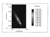
- FIG. 9 is an image showing the intensity distribution of light incident on the first light reflecting surface of the light emitting device according to the present embodiment.
- FIG. 10 is an image showing the intensity distribution of light incident on the second light reflecting surface of the light emitting device according to the present embodiment.
- FIG. 11 is an image showing the intensity distribution of light incident on the third light reflecting surface of the light emitting device according to the present embodiment.
- the first light emitting element 220A, the second light emitting element 220B, and the third light emitting element 220C are semiconductor laser elements.
- the X-Direction is the coordinate value in the first straight line L1 direction of FIGS. 6 and 7, and the Y-Direction is the coordinate value of the second straight line L2 direction of FIGS. 6 and 7. ..
- both the strong light intensity portion and the weak light intensity portion are black due to the monochrome processing, but the black color in the central portion of the light of the elliptical FFP is the strong light intensity portion.
- the black color on the outer periphery of the light of FFP is a portion where the light intensity is weak.
- the major axis direction of the elliptical FFP of the emitted light of the first light emitting element 220A is approximately oriented in the second straight line L2 direction of FIGS. 6 and 7.
- the major axis direction of the elliptical FFP of the emitted light of the second light emitting element 220B is oblique with respect to the second straight line L2 direction of FIGS. 6 and 7.
- the major axis direction of the elliptical FFP of the emitted light of the third light emitting element 220C is oblique with respect to the second straight line L2 direction of FIGS. 6 and 7.
- the major axis direction of the elliptical FFP in FIG. 10 and the major axis direction of the elliptical FFP in FIG. 11 are substantially axisymmetric with respect to the second straight line L2.
- the light from the plurality of light emitting elements 220 reflected by each light reflecting surface approaches each other and is incident on the light extraction region of the light emitting device 200, and is 3 on the light incident surface of the wavelength conversion member 290.
- the two lights overlap. That is, on the incident surface of the light extraction region, the light from the plurality of light emitting elements 220 is arranged in parallel with each other in a plan view parallel to the incident surface.
- the plurality of light emitting elements 220 are semiconductor laser elements, this relationship holds in the major axis direction or the minor axis direction of the elliptical FFP.
- the parallelism here includes a difference of ⁇ 5 degrees.
- the light emitted from each light emitting element 220 includes the light emitted to a specific point on any of the light reflecting surfaces. Further, the light irradiated to this specific point is incident on the incident surface of the light extraction region. At this time, the distance between the two points on the incident surface of the light extraction region is smaller than the distance between the two points on the light reflecting surface. Further, the magnitude relationship between the two points in the light reflecting surface and the light extraction region is established at any irradiation point where the light of the main portion is irradiated.
- the light from a plurality of light emitting elements 220 having the same light emission shape (for example, FFP in the case of a semiconductor laser element) emitted from the light emitting surface has a high proportion of light on the incident surface of the light in the light extraction region.
- FFP light emission shape
- the emission shapes of the light emitted from the plurality of light emitting elements 220 for example, 50% or more of the light of the main part can be overlapped, and further, 80% or more of the light of the main part can be overlapped. ..
- the ratio here can be obtained based on the area of the light emitting shape of FFP.
- the light emitting device 200 has at least three or more light emitting elements (first light emitting element 220A, second light emitting element 220B, third light emitting element 220C), so that the brightness of the light emitted from the light emitting device 200 is high. Can be enhanced.
- each light emitting element serves as a heat source, but in the light emitting device 200, the first light emitting element 220A, the second light emitting element 220B, and the third light emitting element 220C are placed on opposite sides to the light reflecting member.
- the arrangement of a plurality of light emitting elements serving as heat sources is dispersed.
- the distance between the light emitting elements becomes long, and even when the light emitting element becomes a heat source, the concentration of the heat source can be suppressed, so that the possibility that the light emitting efficiency of the light emitting element is lowered or the light emitting element is damaged can be reduced.
- FIG. 12 is a diagram illustrating a modified example of the light reflecting surface. As shown in FIG. 12, each light reflecting surface may be composed of a plurality of regions.
- the first light reflecting surface 241 includes a first reflecting region 241a and a second reflecting region 241b provided at a position farther from the first light emitting element 220A than the first reflecting region 241a.
- the inclination angle of the second reflection region 241b with respect to the lower surface of the first light reflection member 240A is larger than the inclination angle of the first reflection region 241a with respect to the lower surface of the first light reflection member 240A.
- the first reflection region 241a and the second reflection region 241b were the light reflected on the side of the light reflected by the first reflection region 241a close to the second reflection region 241b and the light reflected by the second reflection region 241b.
- the light reflected on the side of the light close to the first reflection region 241a intersects until it reaches the incident surface of the wavelength conversion member 290, and is formed so as to irradiate both ends of the incident surface of the wavelength conversion member 290. Has been done.
- a portion of the light reflected in the first reflection region 241a having a relatively high light intensity and a portion of the light reflected in the second reflection region 241b having a relatively high light intensity intersect in the optical path.
- the incident surface of the wavelength conversion member 290 may be provided with a first reflection region 241a and a second reflection region 241b so as to be irradiated with uniform light intensity. Even in this case, a certain effect can be obtained as compared with a conventional light emitting device having a high light intensity in the central portion.
- the first reflection region 241a and the second reflection region 241b are provided so as to change only the light intensity distribution in the longitudinal direction of the elliptical light irradiated to the first light reflection member 240A. That is, the first reflection region 241a and the second reflection region 241b are provided so that the light intensity distribution in the longitudinal direction does not become too high in the central portion without changing the light intensity distribution in the lateral direction. This is because the FFP of the first light emitting element 220A is particularly easy to spread in the longitudinal direction, and a greater effect can be obtained by controlling the light intensity distribution in the longitudinal direction.
- the first reflection region 241a and the second reflection region 241b are flat surfaces. That is, the light reflecting surface of the first light reflecting member 240A is composed of two planes. This not only facilitates the design of the first light reflecting member 240A, but also provides a margin in the allowable range of mounting deviation. Further, since the first reflection region 241a and the second reflection region 241b are flat surfaces, it becomes easy to form the first light reflection member 240A. Although the light reflecting surface is composed of two planes here, it may be composed of three or more planes. When the light intensity at both ends of the incident surface of the wavelength conversion member 290 is higher than the light intensity at the central portion, the light reflecting surface is formed by an even number of planes. Further, the first reflection region 241a and the second reflection region 241b may be curved surfaces, respectively.
- the second light reflecting surface 242 is provided at a position separated from the first reflecting region 242a and the first reflecting region 242a from the second light emitting element 220B. Also includes a second reflection region 242b. Further, the third light reflecting surface 243 includes a first reflecting region 243a and a second reflecting region 243b provided at a position farther from the third light emitting element 220C than the first reflecting region 243a. The technical significance of configuring the second light reflecting surface 242 and the third light reflecting surface 243 from a plurality of regions is the same as in the case of the first light reflecting surface 241.
- the light emitting device 200 can be used for, for example, an in-vehicle headlight. Further, the light emitting device 200 is not limited to this, and can be used as a light source for lighting, a projector, a head-mounted display, and other display backlights.
- Light emitting device 210 Base 210a Top surface 210b Bottom surface 210c Inner side surface 210d Outer side surface 210e Bottom surface 212 Stepped portion 215, 216 Metal film 220A First light emitting element 220B Second light emitting element 220C Third light emitting element 230 Submount 240A First light reflecting member 240B 2nd light reflecting member 240C 3rd light reflecting member 241 1st light reflecting surface 241a, 242a, 243a 1st reflecting area 241b, 242b, 243b 2nd reflecting area 242 2nd light reflecting surface 243 3rd light reflecting surface 250 Protective element 260 Temperature measuring element 270 Wiring 280 Sealing member 290 Frequency conversion member 291 Frequency conversion unit 292 Light reflection unit 300 Light-shielding member
Landscapes
- Physics & Mathematics (AREA)
- Engineering & Computer Science (AREA)
- Microelectronics & Electronic Packaging (AREA)
- Condensed Matter Physics & Semiconductors (AREA)
- General Physics & Mathematics (AREA)
- Optics & Photonics (AREA)
- General Engineering & Computer Science (AREA)
- Electromagnetism (AREA)
- Power Engineering (AREA)
- Spectroscopy & Molecular Physics (AREA)
- Computer Hardware Design (AREA)
- Manufacturing & Machinery (AREA)
- Led Device Packages (AREA)
Abstract
Priority Applications (2)
| Application Number | Priority Date | Filing Date | Title |
|---|---|---|---|
| JP2022571560A JPWO2022138733A1 (fr) | 2020-12-24 | 2021-12-22 | |
| US18/258,880 US20240044475A1 (en) | 2020-12-24 | 2021-12-22 | Light emitting device |
Applications Claiming Priority (2)
| Application Number | Priority Date | Filing Date | Title |
|---|---|---|---|
| JP2020215688 | 2020-12-24 | ||
| JP2020-215688 | 2020-12-24 |
Publications (1)
| Publication Number | Publication Date |
|---|---|
| WO2022138733A1 true WO2022138733A1 (fr) | 2022-06-30 |
Family
ID=82159807
Family Applications (1)
| Application Number | Title | Priority Date | Filing Date |
|---|---|---|---|
| PCT/JP2021/047608 WO2022138733A1 (fr) | 2020-12-24 | 2021-12-22 | Dispositif électroluminescent |
Country Status (3)
| Country | Link |
|---|---|
| US (1) | US20240044475A1 (fr) |
| JP (1) | JPWO2022138733A1 (fr) |
| WO (1) | WO2022138733A1 (fr) |
Citations (8)
| Publication number | Priority date | Publication date | Assignee | Title |
|---|---|---|---|---|
| JP2000251308A (ja) * | 1999-02-24 | 2000-09-14 | Sony Corp | 集積光学素子及び光学ヘッド並びに記録及び/又は再生装置 |
| US20160087399A1 (en) * | 2013-05-07 | 2016-03-24 | Osram Opto Semiconductors Gmbh | Laser Diode Apparatus |
| JP2016127022A (ja) * | 2014-12-25 | 2016-07-11 | 日亜化学工業株式会社 | 光源装置 |
| JP2018190805A (ja) * | 2017-04-28 | 2018-11-29 | 日亜化学工業株式会社 | 半導体レーザ装置 |
| JP2019134017A (ja) * | 2018-01-30 | 2019-08-08 | 日亜化学工業株式会社 | 発光装置 |
| JP2019161062A (ja) * | 2018-03-14 | 2019-09-19 | 豊田合成株式会社 | 発光装置 |
| WO2019187784A1 (fr) * | 2018-03-26 | 2019-10-03 | パナソニック株式会社 | Dispositif optique |
| JP2019220672A (ja) * | 2018-06-15 | 2019-12-26 | 日亜化学工業株式会社 | 半導体装置の製造方法 |
-
2021
- 2021-12-22 JP JP2022571560A patent/JPWO2022138733A1/ja active Pending
- 2021-12-22 US US18/258,880 patent/US20240044475A1/en active Pending
- 2021-12-22 WO PCT/JP2021/047608 patent/WO2022138733A1/fr active Application Filing
Patent Citations (8)
| Publication number | Priority date | Publication date | Assignee | Title |
|---|---|---|---|---|
| JP2000251308A (ja) * | 1999-02-24 | 2000-09-14 | Sony Corp | 集積光学素子及び光学ヘッド並びに記録及び/又は再生装置 |
| US20160087399A1 (en) * | 2013-05-07 | 2016-03-24 | Osram Opto Semiconductors Gmbh | Laser Diode Apparatus |
| JP2016127022A (ja) * | 2014-12-25 | 2016-07-11 | 日亜化学工業株式会社 | 光源装置 |
| JP2018190805A (ja) * | 2017-04-28 | 2018-11-29 | 日亜化学工業株式会社 | 半導体レーザ装置 |
| JP2019134017A (ja) * | 2018-01-30 | 2019-08-08 | 日亜化学工業株式会社 | 発光装置 |
| JP2019161062A (ja) * | 2018-03-14 | 2019-09-19 | 豊田合成株式会社 | 発光装置 |
| WO2019187784A1 (fr) * | 2018-03-26 | 2019-10-03 | パナソニック株式会社 | Dispositif optique |
| JP2019220672A (ja) * | 2018-06-15 | 2019-12-26 | 日亜化学工業株式会社 | 半導体装置の製造方法 |
Also Published As
| Publication number | Publication date |
|---|---|
| JPWO2022138733A1 (fr) | 2022-06-30 |
| US20240044475A1 (en) | 2024-02-08 |
Similar Documents
| Publication | Publication Date | Title |
|---|---|---|
| TWI817708B (zh) | 光源 | |
| US20150077972A1 (en) | Light emitting device | |
| JP6089686B2 (ja) | 発光装置 | |
| JP7235944B2 (ja) | 発光装置及び発光装置の製造方法 | |
| TW201909452A (zh) | 發光裝置、整合式發光裝置及發光模組 | |
| US11962121B2 (en) | Light emitting device | |
| TW202034598A (zh) | 發光裝置及光學裝置 | |
| JP2022031299A (ja) | 光学部材の製造方法、光学部材、発光装置の製造方法、及び、発光装置 | |
| WO2022138733A1 (fr) | Dispositif électroluminescent | |
| JP2022185010A (ja) | 発光装置 | |
| WO2021251233A1 (fr) | Dispositif électroluminescent | |
| JP7206494B2 (ja) | 発光装置の製造方法、発光装置 | |
| JP2023173809A (ja) | 発光装置 | |
| US11719415B2 (en) | Wavelength conversion member, method of manufacturing same, and light-emitting device | |
| JP2022057984A (ja) | 発光部材及びその製造方法、光学部材、発光装置 | |
| US20220173280A1 (en) | Light-transmissive member and method of manufacturing the same, optical member, and light emitting device | |
| JP2023173810A (ja) | 発光装置 | |
| JP2023047990A (ja) | 光学部材、発光装置 | |
| JP7481610B2 (ja) | 発光装置 | |
| JP2022057819A (ja) | 発光装置 | |
| US20230387360A1 (en) | Light-emitting device | |
| JP6828715B2 (ja) | 光源モジュール | |
| JP2022086988A (ja) | 透光性部材及びその製造方法、光学部材、発光装置 | |
| JP2024000863A (ja) | 発光装置 | |
| JP2021196557A (ja) | 光学部材、及び、発光装置 |
Legal Events
| Date | Code | Title | Description |
|---|---|---|---|
| 121 | Ep: the epo has been informed by wipo that ep was designated in this application |
Ref document number: 21910873 Country of ref document: EP Kind code of ref document: A1 |
|
| ENP | Entry into the national phase |
Ref document number: 2022571560 Country of ref document: JP Kind code of ref document: A |
|
| WWE | Wipo information: entry into national phase |
Ref document number: 18258880 Country of ref document: US |
|
| NENP | Non-entry into the national phase |
Ref country code: DE |
|
| 122 | Ep: pct application non-entry in european phase |
Ref document number: 21910873 Country of ref document: EP Kind code of ref document: A1 |