WO2022138583A1 - 半導体集積回路の製造方法、半導体デバイスの製造方法、および露光装置 - Google Patents
半導体集積回路の製造方法、半導体デバイスの製造方法、および露光装置 Download PDFInfo
- Publication number
- WO2022138583A1 WO2022138583A1 PCT/JP2021/047074 JP2021047074W WO2022138583A1 WO 2022138583 A1 WO2022138583 A1 WO 2022138583A1 JP 2021047074 W JP2021047074 W JP 2021047074W WO 2022138583 A1 WO2022138583 A1 WO 2022138583A1
- Authority
- WO
- WIPO (PCT)
- Prior art keywords
- semiconductor integrated
- circuit
- integrated circuit
- exposure apparatus
- substrate
- Prior art date
- Legal status (The legal status is an assumption and is not a legal conclusion. Google has not performed a legal analysis and makes no representation as to the accuracy of the status listed.)
- Ceased
Links
Images






Classifications
-
- G—PHYSICS
- G03—PHOTOGRAPHY; CINEMATOGRAPHY; ANALOGOUS TECHNIQUES USING WAVES OTHER THAN OPTICAL WAVES; ELECTROGRAPHY; HOLOGRAPHY
- G03F—PHOTOMECHANICAL PRODUCTION OF TEXTURED OR PATTERNED SURFACES, e.g. FOR PRINTING, FOR PROCESSING OF SEMICONDUCTOR DEVICES; MATERIALS THEREFOR; ORIGINALS THEREFOR; APPARATUS SPECIALLY ADAPTED THEREFOR
- G03F7/00—Photomechanical, e.g. photolithographic, production of textured or patterned surfaces, e.g. printing surfaces; Materials therefor, e.g. comprising photoresists; Apparatus specially adapted therefor
- G03F7/20—Exposure; Apparatus therefor
-
- H—ELECTRICITY
- H10—SEMICONDUCTOR DEVICES; ELECTRIC SOLID-STATE DEVICES NOT OTHERWISE PROVIDED FOR
- H10B—ELECTRONIC MEMORY DEVICES
- H10B20/00—Read-only memory [ROM] devices
- H10B20/27—ROM only
- H10B20/30—ROM only having the source region and the drain region on the same level, e.g. lateral transistors
- H10B20/38—Doping programmed, e.g. mask ROM
-
- H—ELECTRICITY
- H10—SEMICONDUCTOR DEVICES; ELECTRIC SOLID-STATE DEVICES NOT OTHERWISE PROVIDED FOR
- H10D—INORGANIC ELECTRIC SEMICONDUCTOR DEVICES
- H10D84/00—Integrated devices formed in or on semiconductor substrates that comprise only semiconducting layers, e.g. on Si wafers or on GaAs-on-Si wafers
- H10D84/01—Manufacture or treatment
- H10D84/0123—Integrating together multiple components covered by H10D12/00 or H10D30/00, e.g. integrating multiple IGBTs
- H10D84/0126—Integrating together multiple components covered by H10D12/00 or H10D30/00, e.g. integrating multiple IGBTs the components including insulated gates, e.g. IGFETs
-
- H—ELECTRICITY
- H10—SEMICONDUCTOR DEVICES; ELECTRIC SOLID-STATE DEVICES NOT OTHERWISE PROVIDED FOR
- H10D—INORGANIC ELECTRIC SEMICONDUCTOR DEVICES
- H10D84/00—Integrated devices formed in or on semiconductor substrates that comprise only semiconducting layers, e.g. on Si wafers or on GaAs-on-Si wafers
- H10D84/01—Manufacture or treatment
- H10D84/02—Manufacture or treatment characterised by using material-based technologies
- H10D84/03—Manufacture or treatment characterised by using material-based technologies using Group IV technology, e.g. silicon technology or silicon-carbide [SiC] technology
- H10D84/038—Manufacture or treatment characterised by using material-based technologies using Group IV technology, e.g. silicon technology or silicon-carbide [SiC] technology using silicon technology, e.g. SiGe
-
- H—ELECTRICITY
- H10—SEMICONDUCTOR DEVICES; ELECTRIC SOLID-STATE DEVICES NOT OTHERWISE PROVIDED FOR
- H10D—INORGANIC ELECTRIC SEMICONDUCTOR DEVICES
- H10D84/00—Integrated devices formed in or on semiconductor substrates that comprise only semiconducting layers, e.g. on Si wafers or on GaAs-on-Si wafers
- H10D84/80—Integrated devices formed in or on semiconductor substrates that comprise only semiconducting layers, e.g. on Si wafers or on GaAs-on-Si wafers characterised by the integration of at least one component covered by groups H10D12/00 or H10D30/00, e.g. integration of IGFETs
- H10D84/82—Integrated devices formed in or on semiconductor substrates that comprise only semiconducting layers, e.g. on Si wafers or on GaAs-on-Si wafers characterised by the integration of at least one component covered by groups H10D12/00 or H10D30/00, e.g. integration of IGFETs of only field-effect components
- H10D84/83—Integrated devices formed in or on semiconductor substrates that comprise only semiconducting layers, e.g. on Si wafers or on GaAs-on-Si wafers characterised by the integration of at least one component covered by groups H10D12/00 or H10D30/00, e.g. integration of IGFETs of only field-effect components of only insulated-gate FETs [IGFET]
-
- H—ELECTRICITY
- H10—SEMICONDUCTOR DEVICES; ELECTRIC SOLID-STATE DEVICES NOT OTHERWISE PROVIDED FOR
- H10P—GENERIC PROCESSES OR APPARATUS FOR THE MANUFACTURE OR TREATMENT OF DEVICES COVERED BY CLASS H10
- H10P76/00—Manufacture or treatment of masks on semiconductor bodies, e.g. by lithography or photolithography
- H10P76/20—Manufacture or treatment of masks on semiconductor bodies, e.g. by lithography or photolithography of masks comprising organic materials
- H10P76/204—Manufacture or treatment of masks on semiconductor bodies, e.g. by lithography or photolithography of masks comprising organic materials of organic photoresist masks
- H10P76/2041—Photolithographic processes
Definitions
- the present invention relates to a method for manufacturing a semiconductor integrated circuit, a method for manufacturing a semiconductor device, and an exposure apparatus.
- Non-Patent Document 1 A semiconductor integrated circuit to be improved has been proposed.
- the method for manufacturing a semiconductor integrated circuit is a manufacturing method for manufacturing a semiconductor integrated circuit in each of a plurality of regions on a substrate, using the mask pattern fixed to the mask substrate, and the plurality of regions.
- each of the semiconductor integrated circuits is formed in a part of each of the plurality of regions.
- the unique circuits formed in each of the plurality of regions are different from each other.
- the method for manufacturing a semiconductor device is to package a plurality of semiconductor integrated circuits manufactured by the method for manufacturing a semiconductor integrated circuit according to the first aspect into a plurality of semiconductor devices.
- the exposure apparatus includes a substrate holding portion that holds the substrate, a variable shaping mask that sets the shape of the light / dark pattern to be irradiated on the substrate, and a plurality of semiconductor integrated circuits formed on the substrate. It is provided with a pattern determination unit that determines the shape of the light / dark pattern to be exposed to each of the corresponding plurality of regions based on the interrelationship data indicating the mutual relationship between the plurality of semiconductor integrated circuits.
- the exposure apparatus includes a substrate holding portion for holding a substrate, a variable shaping mask for setting the shape of a light / dark pattern to be irradiated on the substrate, and a plurality of semiconductor integrated circuits formed on the substrate.
- a pattern determination unit that determines the shape of the light / dark pattern to be exposed to each of a plurality of corresponding predetermined regions based on unique information consisting of a plurality of bits of digital information to be formed in each of the plurality of semiconductor integrated circuits. To prepare for.
- the figure explaining the process of forming the circuit pattern of the part common to a plurality of semiconductor integrated circuits using a fixed mask The figure explaining the process of forming the circuit pattern of the part common to a plurality of semiconductor integrated circuits using a fixed mask.
- the figure explaining the process of forming a peculiar circuit using a variable shaping mask The figure explaining the process of forming a peculiar circuit using a variable shaping mask.
- the figure explaining the exposure process using a fixed mask and a variable shaping mask The figure explaining the exposure process using a fixed mask and a variable shaping mask.
- the figure explaining the exposure process using a fixed mask and a variable shaping mask The figure explaining the exposure process using a fixed mask and a variable shaping mask.
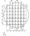
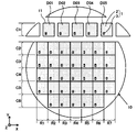
- FIG. 1 is a diagram schematically showing a plurality of semiconductor integrated circuits 1 manufactured on a substrate 10 by the method for manufacturing a semiconductor integrated circuit of the first embodiment.
- the X, Y, and Z directions indicated by the arrows in FIGS. 1 and the following figures are orthogonal to each other, and the X, Y, and Z directions each indicate the same direction in each figure. ing.
- the directions indicated by the arrows are referred to as + X direction, + Y direction, and + Z direction, respectively.
- the position in the X direction is referred to as the X position
- the position in the Y direction is referred to as the Y position
- the position in the Z direction is referred to as the Z position.
- the method for manufacturing the semiconductor integrated circuit 1 of the first embodiment is, for example, to manufacture the semiconductor integrated circuit 1 in each of a plurality of regions 11 on a substrate 10 made of silicon.
- the plurality of semiconductor integrated circuits 1 formed on the substrate 10 include a common circuit 2 which is an electronic circuit common to each semiconductor integrated circuit 1 and a unique circuit 3 representing unique information unique to each semiconductor integrated circuit 1. Is formed.
- each semiconductor integrated circuit 1 includes a common circuit 2 and a unique circuit 3.
- the shape of the semiconductor integrated circuit 1 in the XY plane is rectangular as an example, and the plurality of semiconductor integrated circuits 1 are two-dimensionally formed on the substrate 10 along the X and Y directions. It is arranged and formed.
- each semiconductor integrated circuit 1 may be identified according to the arrangement position, with the arrangement position in the X direction as row (R1 to R7) and the arrangement position in the Y direction as columns (C1 to R6).
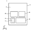
- FIG. 2 is an enlarged view showing one of the semiconductor integrated circuits 1 manufactured by the method for manufacturing a semiconductor integrated circuit according to the first embodiment.
- various circuits including an encryption circuit 22, a decoding circuit 23, and a communication circuit 24, which will be described later, are formed in the portion of the common circuit 2 described above.
- a part of the unique information storage circuit 21 is included in the common circuit 2, and the other part is included in the unique circuit 3 shown by the broken line.
- FIG. 3 is a diagram showing a circuit diagram of an example of the unique information storage circuit 21.
- the unique information storage circuit 21 is, for example, a general NAND type mask ROM circuit, in which a plurality of MOS transistors TR are arranged along a data line DL extending in the Y direction, and X is used at the gate of each MOS transistor TR.
- a selection line SL extending in the direction is connected.
- a voltage application unit 26 and a voltage detection unit 27 are arranged at both ends of each data line DL, respectively.
- a voltage application unit 28 that applies a voltage to the gate of each MOS transistor TR via the selection line SL is arranged.
- a plurality of MOS transistors TR constituting the storage area of the mask ROM circuit are included in the unique circuit 3 shown by the broken line.
- the voltage application units 26 and 28 and the voltage detection unit 27 are not included in the intrinsic circuit 3, but are included in the common circuit 2 shown in FIG.
- a circuit includes not only a completed electric circuit exhibiting one function but also a part of a completed electric circuit to some extent.
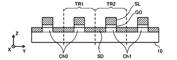
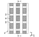
- FIG. 4A shows a top view of the structure of the partial region 25 shown by the broken line in FIG. 3 in the intrinsic circuit 3 which is a mask ROM circuit, as viewed from the + Z direction.
- FIG. 4B is a diagram showing a cross section of a portion along the AA line in FIG. 4A.
- an n-type MOS transistor TR TR1, TR1
- TR1 n-type MOS transistor
- the source / drain region SD is doped with impurity ions such as phosphorus and arsenic at a high concentration.
- the source / drain region SDs of the plurality of MOS transistors TR1 and TR2 arranged at the same X position and arranged in the Y direction are continuously formed in the Y direction.
- the source / drain region SDs of the plurality of MOS transistors TR1 and TR2 and the channel portions Ch0 and Ch1 form a data line DL (see FIG. 3) as a whole.
- the channel portion Ch0 of some MOS transistors such as the MOS transistor TR1 is in an intrinsic semiconductor state with a low concentration of impurity ions.
- the channel portion Ch1 of some MOS transistors such as the MOS transistor TR2 is in an n-type semiconductor state in which the concentration of impurity ions such as phosphorus and arsenic is high, for example.
- the MOS transistor TR2 having the channel portion Ch1 having a high concentration of impurity ions conducts regardless of whether a positive or 0 [V] potential is applied to the selection line SL which is the gate. Therefore, the channel portion Ch1 included in the MOS transistor TR2 stores, for example, a state corresponding to the data “1”.
- the MOS transistor TR1 having the channel portion Ch0 having a low concentration of impurity ions conducts only when a positive potential is applied to the selection line SL which is the gate. Therefore, the channel portion Ch0 included in the MOS transistor TR1 stores, for example, a state corresponding to the data “0”.
- the data stored in the channel portion Ch0 having a low concentration of impurity ions may be set to "1", and the data stored in the channel portion Ch1 having a high concentration of impurity ions may be set to "0".
- the plurality of semiconductor integrated circuits 1 formed on the substrate 10 include the above-mentioned common circuit 2 and the unique circuit 3, respectively.
- the distribution of the concentration of impurity ions in a part of the intrinsic circuit 3, for example, the channel portions Ch0 and Ch1 described above, is different in each of the plurality of semiconductor integrated circuits 1.
- the circuit portion common to the plurality of semiconductor integrated circuits 1 among the unique circuits 3 and the common circuit 2 have a mask pattern fixed to the mask substrate (hereinafter,).
- the mask substrate and the mask pattern are combined and also called a "fixed mask") to be formed by exposure.
- the fixed mask may be a translucent mask in which a light-shielding film such as chromium as a mask pattern or a dielectric transmissive film as a phase shifter is formed on a translucent mask substrate.
- it may be a reflective mask in which an absorbent film as a mask pattern or a stepped shape as a phase shifter is formed on the surface of a reflective mask substrate.
- the circuit portions different from each of the plurality of semiconductor integrated circuits 1 among the unique circuits 3 are formed by exposure using a variable shaping mask.
- the variable shaping mask is a so-called spatial light modulator.
- the reflection type variable shaping mask for example, a mask having a plurality of movable micromirrors formed on the reflection surface or a reflection type liquid crystal display device can be used.
- the transmissive variable shaping mask for example, a transmissive liquid crystal display device can be used. The details of the exposure apparatus using the variable shaping mask will be described later.
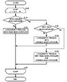
- step S100 is a step corresponding to the start of a loop including a total of N lithography steps.
- the substrate 10 is not limited to one substrate, and may be an aggregate of a plurality of substrates.
- the lithography process is a series of forming a photosensitive film (resist) on a substrate 10, patterning the photosensitive film by exposure and development, and processing the substrate 10 using the patterned photosensitive film.
- the lithography step may include a step of forming a predetermined film on the substrate 10 before forming the photosensitive film.
- the processing of the substrate 10 may be etching, oxidation, nitriding, or ion implantation into the substrate 10 or a predetermined film formed on the substrate 10.
- step S110 it is determined whether or not the jth lithography step is a step of performing exposure using a variable shaping mask. If the determination is denied (No), the process proceeds to step S120, and a lithography process including exposure using a fixed mask is performed.
- step S120 a fixed mask having a circuit pattern forming a common circuit 2 including an encryption circuit 22, a decoding circuit 23, and a communication circuit 24 of the semiconductor integrated circuit 1 is used. Therefore, in step S120, a circuit pattern forming a part of the common circuit 2 including the encryption circuit 22, the decoding circuit 23, and the communication circuit 24 is formed on the substrate 10. Since the lithographic process including exposure using a fixed mask is the same as the lithographic process usually used for manufacturing semiconductor integrated circuits, detailed description thereof will be omitted.
- the fixed mask used in step S120 may include a mask pattern corresponding to the circuit pattern of the portion common to the plurality of semiconductor integrated circuits 1 in the unique circuit 3.
- a part of the circuit pattern of the portion common to the plurality of semiconductor integrated circuits 1 of the intrinsic circuit 3 is also formed on the substrate 10. Will be done.
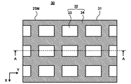
- FIG. 7A is a diagram showing an example of a fixed mask 30 for forming a circuit pattern of a portion common to a plurality of semiconductor integrated circuits 1.
- the fixed mask 30 includes a translucent mask substrate 31 and a mask pattern 32 formed on the surface of the mask substrate 31 for forming a source / drain region SD in the unique information storage circuit 21 as an example.
- the mask pattern 32 includes a light-transmitting portion 33 and a light-shielding portion 34.
- FIG. 7A shows the mask pattern 32 corresponding to the portion 25M corresponding to the partial region 25 shown in FIGS. 3 and 5 of the source / drain region SD in the intrinsic information storage circuit 21.
- the AA line in FIG. 7A is shown at a position on the mask pattern 32 corresponding to the AA line shown in FIG.
- the mask pattern 32 may include a portion other than the partial region 25 of the unique information storage circuit 21, and a mask pattern corresponding to other circuits such as the encryption circuit 22, the decoding circuit 23, and the communication circuit 24. ..
- the mask pattern 32 does not include the pattern in the partial region 25 of the unique information storage circuit 21, but includes only the mask pattern corresponding to other circuits such as the encryption circuit 22, the decoding circuit 23, and the communication circuit 24. You may stay.
- FIG. 7B is a diagram showing a process of forming a source / drain region SD in a portion corresponding to the unique circuit 3 in each region 11 on the substrate 10 by using the fixed mask 30 shown in FIG. 7A.
- FIG. 7B is a cross-sectional view of the substrate 10 on the AA line shown in FIG.
- a photosensitive film 26 such as a photoresist is formed on the substrate 10, and the photosensitive film 26 is exposed to light using a fixed mask 30 to expose the photosensitive film 26 in a portion corresponding to the translucent portion 33. Then, the exposed portion of the photosensitive film 26 is removed by development to form an opening 26o, and the surface of the substrate 10 is exposed from the opening 26o.
- the source / drain region SD is located in a portion other than the partial region 25 of the unique information storage circuit 21, and in a predetermined portion in other circuits such as the encryption circuit 22, the decryption circuit 23, and the communication circuit 24. May be formed.
- step S120 After the process of step S120 is completed, the process proceeds to step S160, and the loop from step S110 to step S160 is repeated until the process of N times is completed.
- step S110 If the judgment in step S110 is affirmed (Yes), the process proceeds to step S130.
- step S130 it is determined whether or not the j-th lithography step is a step of performing exposure using a fixed mask in addition to exposure using a variable shaping mask. If the determination is denied (No), the process proceeds to step S140, and a lithography process including exposure using a variable shaping mask is performed.
- step S140 a plurality of semiconductor integrated circuits 1 form different circuit patterns for the unique circuit 3 of the unique information storage circuit 21. However, as will be described later with reference to FIG. 12, for some semiconductor integrated circuits 1, the same pattern may be formed in the intrinsic circuit 3.
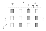
- FIG. 8A is a diagram showing the shape (brightness distribution) of the light / dark pattern 35 formed on the substrate 10 using the variable shaping mask.
- the AA line in FIG. 8A is shown at a position corresponding to the AA line shown in FIG. FIG. 8A shows only the pattern in the small area 25E corresponding to the partial area 25 among the light and dark patterns 35, but the light and dark pattern 35 may have an area corresponding to all of the intrinsic circuit 3. good.
- FIG. 8B is a diagram illustrating a method of injecting ions having a predetermined impurity concentration into each of the channel portions Ch0 and Ch1 of a plurality of MOS transistors TR included in the intrinsic circuit 3 by using the light / dark pattern 35 shown in FIG. 8A. Is. FIG. 8B is a cross-sectional view of the substrate 10 on the AA line shown in FIG.
- step S140 a photosensitive film 27 such as a photoresist is formed on the substrate 10, and the light-dark pattern 35 formed by the variable shaping mask is exposed to the photosensitive film 27.
- the shape (brightness distribution) of the light / dark pattern 35 is set so that the portion corresponding to the channel portion Ch1 becomes the bright portion 36 and the other portion becomes the dark portion 37. That is, the variable shaping mask is set so that the portion 38 corresponding to the channel portion Ch0 becomes the dark portion 37 like the portion 39 corresponding to the portions other than the channel portion Ch0 and the channel portion Ch1.
- the light-dark pattern 35 can be made different for each semiconductor integrated circuit 1 formed in each region 11 in the substrate 10.
- the photosensitive film 27 in the portion exposed by the bright portion 36 is removed by the subsequent development to become the opening 27o, and the surface of the substrate 10 is exposed from the opening 27o. Then, using the remaining photosensitive film 27, that is, the patterned photosensitive film 27 as a mask, arsenic or phosphorus is ion-implanted into the substrate 10 as an example, and impurity ions having a predetermined concentration are implanted into the channel portion Ch1. ..
- step S140 a predetermined impurity ion concentration distribution can be formed in each channel portion of the plurality of MOS transistors constituting the NAND mask ROM as an example of the unique information storage circuit 21.
- 1-bit data "1" is stored in the channel portion Ch1 doped with impurity ions at a high concentration, and 1 bit is stored in the channel portion Ch0 not doped with impurity ions (at a low concentration).
- Data "0" is stored. Therefore, if there are M MOS transistors TR each having a channel portion in the intrinsic circuit 3, the intrinsic circuit 3 can store the information of M bits.
- each part of the plurality of regions 11 on the substrate 10 represents the unique information unique to each semiconductor integrated circuit 1, and forms a unique circuit 3 in which at least a part of each circuit pattern is different. can do. It can be said that the distribution of the concentration of impurity ions in the channel portions Ch0 and Ch1 described above is also a circuit pattern.
- step S140 After the process of step S140 is completed, the process proceeds to step S160, and the loop from step S110 to step S160 is repeated until the process of N times is completed.
- step S150 If the determination in step S130 is affirmed (Yes), the process proceeds to step S150.
- FIG. 10A, FIG. 10B, and FIG. 10C are diagrams for explaining the lithography process in step S150.
- step S150 in addition to exposure using a fixed mask, exposure using a variable shaping mask is also performed. Is.
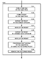
- step S150 as shown in the flow of FIG. 9, first, in step S151, a thin film is formed on the substrate 10. If it is not necessary to form a thin film, step S151 may be omitted.
- step S152 a photosensitive film 26 such as a photoresist is formed on the substrate 10.
- step S153 the photosensitive film 26 is exposed using the fixed mask 30 as shown in FIG. 7A.
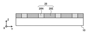
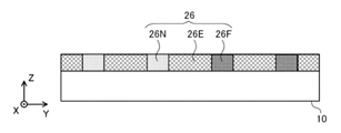
- FIG. 10A shows a cross-sectional view of the substrate 10 and the photosensitive film 26 after exposure using the fixed mask 30. Note that FIG. 10A is a cross-sectional view of the substrate 10 on the AA line of FIG. 5, similarly to FIGS. 7B and 8B.
- the photosensitive portion 26E is formed on the photosensitive film 26. The portion not exposed by the exposure using the fixed mask 30 remains as the non-photosensitive portion 26N.
- step S154 the photosensitive film 26 is developed.
- the photosensitive film 26 after development is in the same state as the photosensitive film 26 shown in FIG. 7B.
- step S155 the remaining photosensitive film 26 is exposed to the light-dark pattern 35 formed by the variable shaping mask as shown in FIG. 8A.
- step S156 the photosensitive film 26 is developed again.
- FIG. 10C the developed photosensitive film 26 is exposed only to the non-photosensitive portion 26N which was not exposed to either the exposure using the fixed mask 30 in step S153 or the exposure using the variable shaping mask in step S155. It remains on the substrate 10.
- the process proceeds to step S157, and the substrate 10 is processed using the photosensitive film 26 in which the non-photosensitive portion 26N shown in FIG. 10C remains, that is, the patterned photosensitive film 26.
- the treatment for the substrate 10 is, for example, ion implantation of arsenic or phosphorus into the substrate 10, and the source / drain region SD and the channel portion Ch1 are simultaneously formed by this ion implantation. ..
- the channel portion Ch0 is covered with the photosensitive film 26, ion implantation is not performed.
- the ion implantation may be performed on the thin film formed on the substrate 10 instead of the substrate 10.
- the photosensitive film 26 was developed after the exposure using the fixed mask and after the exposure using the variable shaping mask, respectively, but after the exposure using the fixed mask. Development (development in step S154) may be omitted.
- the photosensitive film 26 after the execution of step S155 has a photosensitive portion 26E exposed to the fixed mask 30 and a photosensitive portion 26F exposed to the variable shaping mask. And the non-photosensitive portion 26N that was not exposed to any exposure are formed.
- the photosensitive film 26 in this state may be developed in step S156 to form the photosensitive film 26 (non-photosensitive portion 26N) in the state shown in FIG. 10C.
- the exposure using the variable shaping mask is performed after the exposure using the fixed mask, but the exposure using the fixed mask may be performed after the exposure using the variable shaping mask. ..
- variable shaping mask is used to apply unique information unique to each semiconductor integrated circuit 1 to each part of the plurality of regions 11 on the substrate 10. It is possible to form a unique circuit 3 that represents and at least a part of each circuit pattern is different.
- step S150 After the process of step S150 is completed, the process proceeds to step S160, and the loop from step S110 to step S160 is repeated until the process of N times is completed.
- step S160 the individual semiconductor integrated circuits 1 may be cut (individualized) from the substrate 10 as described later.
- a selection line SL as a gate is formed on the ion-implanted channel portion Ch1 and the non-ion-implanted channel portion Ch0 in the subsequent steps. Therefore, it is difficult to analyze the concentration of impurity ions in each channel portion Ch0 and Ch1 only by observing the completed semiconductor integrated circuit 1 from the upper surface. Therefore, in the above-mentioned method, it is possible to reduce the possibility that the unique information stored in the unique circuit 3 is reverse engineered.
- the processing of the substrate 10 using the patterned photosensitive films 26 and 27 is not limited to the ion implantation described above. That is, the processing of the substrate 10 may be other processing such as etching, oxidation, and nitriding of a predetermined film formed on the substrate 10 or the substrate 10. Further, even if a groove or a hole is formed by performing a predetermined etching on the substrate 10 or a predetermined film formed on the substrate 10, a conductor such as a metal is partially embedded in the groove or the hole. good.
- steps S120 and S140 as in step S150, a step of forming a predetermined film on the substrate 10 before forming the photosensitive films 26 and 27 on the substrate 10 may be included. Further, a PEB treatment for heating the photosensitive films 26 and 27 may be included after the exposure using the fixed mask 30 or the exposure using the variable shaping mask and before the development.
- the unique information storage circuit 21 including the unique circuit 3 which represents the unique information unique to each semiconductor integrated circuit 1 and at least a part of each circuit pattern is different, and the unique information storage circuit 21 includes the above-mentioned NAND mask. It is not limited to ROM. Therefore, the pattern peculiar to each semiconductor integrated circuit 1 in the peculiar circuit 3 is not limited to the above-mentioned concentration distribution of impurity ions.
- the pattern peculiar to the semiconductor integrated circuit 1 in the peculiar circuit 3 may be the presence or absence of a specific transistor in the circuit constituting the electronic element, the difference in the gate length, the difference in the gate width, and the like. Alternatively, the presence / absence or size difference of a connection portion such as a specific via hole in the circuit constituting the electronic element may be used.
- the circuit may be a circuit in which the signal "1" or the signal "0" is stored depending on the difference in the operating characteristics of the electronic element caused by the presence or absence of these and the difference in size.
- steps S140 and S150 described above the channel portions Ch0 and Ch1 which are unique patterns representing the unique information unique to the semiconductor integrated circuit 1 in the unique circuit 3 are formed by exposure using a variable shaping exposure apparatus. It can be performed by one lithography process including. Therefore, it is possible to reduce the number of times of exposure required by using the variable shaping exposure apparatus, which takes a processing time as compared with the exposure using the fixed mask 30, and it is possible to increase the productivity of the semiconductor integrated circuit 1.
- variable shaping exposure apparatus is not limited to the above-mentioned exposure using light including ultraviolet rays, and may be exposure using charged particle beams such as electron beams.
- a so-called blanking aperture array may be used as the variable shaping mask.
- the plurality of semiconductor integrated circuits 1 are formed in each of the regions 11 two-dimensionally arranged on the substrate 10 along the X direction and the Y direction. Therefore, by arranging the intrinsic circuit 3 at a common position inside each semiconductor integrated circuit 1, the plurality of intrinsic circuits 3 are arranged two-dimensionally along the X direction and the Y direction. ..
- a plurality of unique circuits 3 may be exposed by a single scanning exposure along the Y direction, for example, as shown in FIG. 11 by using an exposure apparatus provided with a variable shaping mask. That is, a plurality of unique circuits 3 included in the semiconductor integrated circuit 1 of the plurality of regions 11 arranged in the row R1 may be exposed by scanning exposure along the scanning path SP1 shown by the broken line. Similarly, a plurality of unique circuits 3 included in the semiconductor integrated circuits 1 of the plurality of regions 11 arranged in the rows R2 to R7 may be exposed by each scanning exposure along the scanning paths SP2 to SP7. ..
- the width AW in the X direction of the intrinsic circuit 3 may be, for example, about 100 ⁇ m or less, and therefore the exposure field of view in the X direction of the exposure apparatus provided with the variable shaping mask may be about 100 ⁇ m or less.
- the exposure apparatus provided with the variable shaping mask will be described later with reference to FIG.
- the scanning directions (moving directions of the substrate 10 at the time of exposure) are mutually reversed, so that the respective scanning paths SP1 are used.
- the moving distance of the substrate 10 between ⁇ SP7 may be reduced. This may further improve the throughput.
- the scanning exposure using the exposure apparatus provided with the variable shaping mask is not limited to the one along the Y direction, and may be the one along the X direction.
- the Y direction (or X direction) can be referred to as the first direction
- the X direction (or Y direction) can be referred to as the second direction intersecting the Y direction (or X direction) which is the first direction.
- the encryption key is an encryption key used when the signal transmitted or received by the semiconductor integrated circuit 1 is encrypted by the encryption circuit 22 or decoded by the decryption circuit 23.
- As the encryption key a 4-byte hexadecimal code value such as 0x34F23E1A is used. Therefore, the unique circuit 3 in the unique information storage circuit 21 of the semiconductor integrated circuit 1 formed in each region 11 on the substrate 10 has a value according to the purpose of use of the semiconductor integrated circuit 1 formed in each region 11. To memorize the encryption key of.
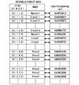
- the interrelationship data is data showing the mutual relationship between one of the plurality of semiconductor integrated circuits 1 to be manufactured and the other one or the other.
- the interrelationship data includes the substrate number W of the substrate 10 on which each semiconductor integrated circuit 1 is formed, the arrangement position (column) C in the Y direction on the substrate 10, and the arrangement position in the X direction (the arrangement position in the X direction).
- Row) Data showing the relationship of each of the semiconductor integrated circuits 1 specified by R with other semiconductor integrated circuits 1.
- An IC (W, C, R) control number (IC N0.) Is assigned to the semiconductor integrated circuit 1 arranged at the position of the substrate number W, that is, the column C and the row R of the Wth substrate. There is.
- the semiconductor integrated circuit 1 having the control number IC (1, 1, 2) is the semiconductor integrated circuit 1 that should be the master chip in the plurality of semiconductor integrated circuits 1 of the first set.
- a code (INDEX) called Master-1 is assigned to indicate that.
- the unique information storage circuit 21 of the semiconductor integrated circuit 1 having the control number IC (1, 1, 2) has an encryption key 0x34F23E1A that causes the unique information storage circuit 21 to function as a master chip in the plurality of semiconductor integrated circuits 1 of the first set. To memorize.
- the semiconductor integrated circuit 1 having the control number IC (1, 1, 3) is a Slave indicating that the semiconductor integrated circuit 1 should be the first slave chip in the plurality of semiconductor integrated circuits 1 of the first set.
- the code -1-1 is assigned.
- the unique information storage circuit 21 of the semiconductor integrated circuit 1 having the control number IC (1, 1, 3) functions as the first slave chip in the plurality of semiconductor integrated circuits 1 of the first set.
- the semiconductor integrated circuit 1 having the control number IC (1, 1, 4) corresponds to the assigned code Slave-1-2, which is used in the first set of the plurality of semiconductor integrated circuits 1.
- the semiconductor integrated circuit 1 having the control number IC (1, 2, 5) corresponds to the code assigned to Master-2, which is included in the second set of the plurality of semiconductor integrated circuits 1.
- Slave-2 is assigned to the semiconductor integrated circuit 1 of the control number IC (1,2,6) and the control number IC (1,2,7).
- the same encryption key 0x59C6AF32 which is used as a slave chip in the second set of a plurality of semiconductor integrated circuits 1 is stored.
- the semiconductor integrated circuit 1 of the control number IC (1,4,4), the control number IC (1,4,5), and the control number IC (1,4,6) is assigned.
- the circuit 1 stores a common encryption key 0xC4A25D3B which corresponds to the assigned code of Group-2 and which is used as a plurality of semiconductor integrated circuits 1 belonging to the set of Group-2.
- the encryption key is not limited to the 4-byte hexadecimal code described above, and may be digital data having an arbitrary number of bits. Further, instead of the encryption key itself, it may be, for example, digital data obtained as a result of performing a predetermined operation on the encryption key.
- the encryption key itself and the digital data obtained as a result of performing a predetermined operation on the encryption key are hereinafter also referred to as "information about the encryption key".
- the plurality of semiconductor integrated circuits 1 manufactured by the manufacturing method of the first embodiment is one or a plurality of other semiconductor integrated circuits 1 associated with a code corresponding to information about an encryption key stored in each unique circuit 3. Communication with encryption and decryption is possible only for the semiconductor integrated circuit 1. Conversely, by forming a plurality of semiconductor integrated circuits 1 with a circuit pattern that is generally common and changing some of the circuit patterns in the intrinsic circuit 3, another specific one or a plurality of semiconductor integrated circuits. It is possible to manufacture a semiconductor integrated circuit 1 capable of communicating with only 1.
- the unique information stored in the unique circuit 3 is not limited to the above-mentioned encryption key, and may be, for example, identification information representing each semiconductor integrated circuit 1.
- the semiconductor manufacturer who implements the method for manufacturing the semiconductor integrated circuit 1 of the first embodiment may determine the unique information such as the encryption key stored in the unique circuit 3. Further, the semiconductor manufacturer may also determine the correspondence between the unique information and each code included in the interrelationship data. Alternatively, the consignor who outsources the manufacture of the semiconductor integrated circuit 1 to the semiconductor manufacturer may determine the above-mentioned unique information or the correspondence between the respective unique information and the code.
- the semiconductor manufacturer determines the correspondence between the unique information and the code contained in the interrelationship data, or when the semiconductor manufacturer determines the unique information, only the semiconductor manufacturer grasps the unique information actually stored in the semiconductor integrated circuit 1. become. Therefore, in this case, since the information regarding the unique information is not known to anyone other than the semiconductor manufacturer, the confidentiality of the unique information such as the encryption key can be highly maintained.
- the correspondence between the unique information and the code contained in the interrelationship data, or the unique information is determined (generated) by the variable shaping exposure apparatus used in the exposure using the variable shaping mask as described later. ) May.
- the unique information actually stored in the semiconductor integrated circuit 1 is information that can be grasped only by the variable shaping exposure apparatus and cannot be known by anyone else. Therefore, in this case, the confidentiality of the unique information can be maintained to a higher degree.
- the interrelationship data may also be generated by the semiconductor manufacturer who implements the method for manufacturing the semiconductor integrated circuit 1 of the first embodiment, or variable shaping exposure used in exposure using a variable shaping mask as described later.
- the device may be generated.
- the interrelationship data may be determined by a consignor who outsources the manufacture of the semiconductor integrated circuit 1 to the semiconductor manufacturer.
- the interrelationship data is generated by the semiconductor manufacturer, or when the variable shaping exposure device is generated, the interrelationship data is generated by the user of the semiconductor integrated circuit 1 (semiconductor integrated circuit 1) together with the manufactured plurality of semiconductor integrated circuits 1. It is good to transfer it to the person who outsourced the production of.
- the user who uses the semiconductor integrated circuit 1 may select and use the semiconductor integrated circuit 1 suitable for the purpose of use from a plurality of semiconductor integrated circuits 1 based on the interrelationship data transferred from the manufacturer. ..
- the manufacturing method of the semiconductor integrated circuit 1 of the first embodiment described above is fixed to the mask substrate 31 in the manufacturing method of manufacturing the semiconductor integrated circuit 1 in each of the plurality of regions 11 on the substrate 10.
- an electronic circuit common circuit 2 as a part of the semiconductor integrated circuit 1 is formed in each of the plurality of regions 11, and a plurality of variable shaping exposure devices having a variable shaping mask are used.
- Each part of the region 11 is provided with a unique circuit 3 representing unique information unique to each semiconductor integrated circuit 1, and the unique circuits 3 formed in each of the plurality of regions 11 are different from each other. ..
- This configuration it is possible to inexpensively manufacture a plurality of semiconductor integrated circuits 1 each having a unique unique circuit 3.
- the electronic circuit which is the common circuit 2 includes at least a part of the circuit for encrypting or decrypting the information (encryption circuit 22 and the decryption circuit 23), and the unique information encrypts or decodes the information. It may be information about the encryption key used at the time of the operation.
- a plurality of semiconductor integrated circuits 1 are formed with a circuit pattern that is generally common, and by changing some circuit patterns in the intrinsic circuit 3, another specific one or a plurality of semiconductor integrated circuits 1 are formed. It is possible to manufacture a semiconductor integrated circuit 1 capable of communicating with only one.
- An electronic circuit (common circuit 2) is formed in each of a plurality of the regions arranged along the first direction on the substrate 10 and the second direction intersecting the first direction, and the unique circuit 3 is formed.
- the formation is performed by scanning the substrate 10 on which the photosensitive film 26 is formed relative to the variable shaping exposure apparatus along the first direction (Y direction), and during scanning, the first direction among the plurality of regions 11. It may include exposing a plurality of regions 11 arranged along (Y direction).
- the formation of the unique pattern (channel portions Ch0, Ch1) in the unique circuit 3 and representing the unique information unique to the semiconductor integrated circuit 1 is a single lithography process including exposure using a variable shaping exposure apparatus. You may go by. As a result, the number of exposures using the variable shaping exposure apparatus can be reduced, and the productivity of the semiconductor integrated circuit 1 can be further increased.
- the electronic circuit includes a NAND mask ROM (unique information storage circuit 21), and the intrinsic circuit 3 includes channel portions Ch0 and Ch1 of a plurality of MOS transistors TR constituting the NAND mask ROM. It may include the concentration distribution of the impurity ion injected into. With this configuration, the number of exposures using the variable shaping exposure apparatus can be reduced, and the productivity of the semiconductor integrated circuit 1 can be further increased.
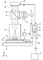
- FIG. 13 is a diagram schematically showing the configuration of the exposure apparatus 50 of the second embodiment.
- the exposure apparatus 50 of the second embodiment is a variable shaping exposure apparatus provided with a variable shaping mask 54 and exposing a light / dark pattern 35 having a variable shape on a substrate 10.
- the variable shaping mask 54 may be any one of the above-mentioned spatial light modulators, but in the present embodiment, a reflection type spatial light modulator in which a plurality of minute reflective surfaces are arranged on the variable mask surface DP is used. It is adopted.
- the exposure device 50 further includes a light transmission optical system 52, a branch element 53, an imaging optical system 55, a substrate holding unit 56, a surface plate 57, a control unit 60, and the like.
- the substrate 10 is placed on the substrate holding portion 56 arranged on the surface plate 57.
- the substrate 10 can be moved in the X direction and the Y direction on the surface plate 57 by the substrate holding portion 56. Further, the substrate 10 can be moved by the substrate holding portion 56 by a minute distance in the Z direction, and can be further rotated (tilted) by a minute angle with the X and Y directions as rotation axes.
- the positions of the substrate 10 in the X direction and the Y direction are measured by the position measuring unit 59 via the position of the scale plate 58 provided on the substrate holding unit 56, and are transmitted to the control unit 60 as the measurement signal S3.
- the control unit 60 sends a position control signal S4 to the substrate holding unit 56 based on the measurement signal S3, and controls the substrate 10 to be arranged at predetermined X and Y positions.
- the control unit 60 sends an exposure control signal S2 to the light source 51 to control the light emission timing and the light emission amount of the light source 51.
- the exposure apparatus 50 may be a scanning type exposure apparatus that exposes the substrate 10 and the substrate holding portion 56 while scanning them relative to the projection optical system 55 in the in-plane direction of the XY plane. In this case, the exposure apparatus 50 may shorten the processing time required for exposing the substrate 10 by performing scanning exposure along the scanning paths SP1 to SP7 shown in FIG.
- exposure is performed with the substrate 10 and the substrate holding portion 56 fixed to the projection optical system 55, and after the exposure is completed, the substrate 10 and the substrate holding portion 56 are sequentially moved with respect to the projection optical system 55.
- It may be a repeat type exposure apparatus.
- the control unit 60 exposes the unique circuit 3 so as not to perform unnecessary exposure on the portion of the common circuit 2 on the substrate 10.
- the light emission of the light source 51 may be stopped.
- the wavelength of the illumination light emitted from the light source 51 is, for example, a wavelength of 450 [nm] or less. As a further example, the wavelength of the illumination light may be 193 [nm] or less.
- the light source 51 may be incorporated inside the exposure apparatus 50 or may be arranged outside the exposure apparatus 50. The illumination light may be guided from the light source 51 to the exposure apparatus 50 by using a light guide member such as an optical fiber.
- the illumination light emitted from the light source 51 is shaped by the light transmission optical system 52, is incident on the branch element 53 such as a beam splitter, is reflected by the branch surface 53s of the branch element 53, and is reflected on the variable mask surface DP of the variable shaping mask 54. Is irradiated to. Then, a part of the illumination light is reflected by a plurality of minute reflecting surfaces (not shown) arranged on the variable mask surface DP, is incident on the branch element 53 again, and is transmitted through the branch surface 53s of the branch element 53. Then, it is incident on the imaging optical system 55.
- the branch element 53 such as a beam splitter
- the variable shaping mask 54 transmits a part of the reflected light through the imaging optical system 55 by changing the angle of the reflecting surface of each of the plurality of minute reflecting members (not shown) arranged on the variable mask surface DP. Reflects in a direction that cannot be done. Alternatively, the positions of the reflecting surfaces of the plurality of adjacent micro-reflecting members in the Z direction are different from each other to generate a phase-offset effect of light, and the light is directed from a predetermined portion of the variable mask surface DP toward the imaging optical system 55. Dimming the reflected light. As a result, the light / dark pattern 35 formed by the variable shaping mask 54 is projected on the surface of the substrate 10.
- the control unit 60 sends a control signal S1 to the variable shaping mask 54 to give a predetermined displacement amount of displacement to a predetermined minute reflective member in the variable mask surface DP, so that the light / dark pattern 35 formed on the surface of the substrate 10 Determine the shape (brightness distribution) of.
- the control unit 60 may include a pattern determination unit 61 and an interrelationship data generation unit 62. Further, the control unit 60 communicates with the external server 70 installed outside the exposure apparatus 50 via the network line NW.
- the pattern determination unit 61 describes the shape (brightness distribution) of the light / dark pattern 35 exposed to the unique circuit 3 portion in the plurality of regions 11 corresponding to the plurality of semiconductor integrated circuits 1 formed on the substrate 10. The determination is made based on the interrelationship data as shown in FIG. Specifically, for example, as shown in FIG. 12, a code (INDEX) for each semiconductor integrated circuit 1 on the substrate 10 is assigned to the interrelationship data received from the external server 70.
- the pattern determination unit 61 determines the unique information to be stored in the unique circuit 3 (for example, the numerical value of the encryption key consisting of the hexadecimal code described above) based on the code shown in the interrelationship data.
- the pattern determination unit 61 determines the shape (brightness distribution) of the light / dark pattern 35 for exposure transfer of the circuit pattern corresponding to the unique information on the substrate 10 based on the determined unique information. Then, the control unit 60 controls the variable shaping mask 54 by the control signal S1 so that the light / dark pattern 35 determined by the pattern determination unit 61 is projected onto the substrate 10.
- An example of the shape of the light / dark pattern 35 is the shape (light / dark distribution) shown in FIG. 8A described above.
- the exposure apparatus 50 is the scanning type exposure apparatus described above
- the light / dark pattern 35 projected on the substrate 10 moves in the X direction or the Y direction in synchronization with the scanning on the substrate 10.
- the variable shaping mask 54 is dynamically controlled.
- the pattern determination unit 61 may have a storage unit 63 that stores the shape data of the light / dark pattern 35 corresponding to the plurality of unique information. In this case, the pattern determination unit 61 may read out one shape data corresponding to the determined unique information from the storage unit 63 and use it. Therefore, the shape data of the light / dark pattern 35 can be determined in a short time as compared with the case where the shape data of the light / dark pattern 35 is generated every time the unique information is determined.
- the storage unit 63 of the pattern determination unit 61 may store the shape data of the light / dark pattern 35 corresponding to the division unique information obtained by dividing the unique information by a predetermined number of bits (1 to 16 as an example). .. In this case, the pattern determination unit 61 may read a plurality of shape data corresponding to the determined unique information from the storage unit 63 and combine the shape data to obtain the shape data of the light / dark pattern 35.
- the shape data stored in the storage unit 63 may be, for example, data representing an image such as bitmap data or TIF data, or may be data generally representing mask data such as GDSII. Further, the shape data stored in the storage unit 63 may be transmitted from the external server 70 or may be generated by the control unit 60.
- the exposure apparatus 50 as the variable shaping exposure apparatus is not limited to the exposure apparatus using light including ultraviolet rays described above, and may be an exposure apparatus using a charged particle beam such as an electron beam.
- a transmissive mask having a so-called blanking aperture array may be used as the variable shaping mask 54.
- the exposure apparatus 50 may include the interrelationship data generation unit 62 that generates the interrelationship data shown in FIG.
- the exposure apparatus 50 determines the unique information to be stored in the unique circuit 3 (for example, the numerical value of the encryption key consisting of the hexadecimal code described above) based on the interrelationship data generated by itself.
- the exposure apparatus 50 of the second embodiment is formed on the substrate 10 with a substrate holding portion 56 for holding the substrate 10, a variable shaping mask 54 for setting the shape of the light / dark pattern 35 to be irradiated on the substrate 10, and a variable shaping mask 54.
- the pattern determination unit 61 that determines the shape of the light / dark pattern 35 to be exposed to each of the plurality of regions 11 corresponding to the plurality of semiconductor integrated circuits 1 based on the interrelationship data indicating the mutual relationship between the plurality of semiconductor integrated circuits 1. And have. With this configuration, it is possible to inexpensively manufacture a plurality of semiconductor integrated circuits 1 each having a unique unique circuit 3.
- the pattern determination unit 61 determines the unique information to be formed in each of the plurality of predetermined regions 11 based on the interrelationship data, and determines the shape of the light / dark pattern 35 based on the determined unique information. good. With this configuration, it is possible to flexibly form a unique circuit 3 in which different unique information is stored for each of the plurality of semiconductor integrated circuits 1.
- the pattern determination unit 61 has a storage unit 63 for storing the shape data of the light / dark pattern 35 corresponding to the plurality of unique information, and even if the shape data corresponding to the determined unique information is read from the storage unit 63. good. Thereby, the shape data of the light / dark pattern 35 can be determined in a shorter time.
- the pattern determining unit 61 determines the shape of the light / dark pattern 35 to be exposed to each of the unique circuits 3 in the plurality of regions 11, and the pattern determination unit 61 mutually determines the shape of the plurality of semiconductor integrated circuits 1. It was decided based on the interrelationship data showing the relationship between them.
- the pattern determination unit 61 is based on the unique information consisting of a plurality of bits of digital information to be stored in the unique circuit 3 (for example, the numerical value of the encryption key consisting of the hexadecimal code described above).
- the shape of the light / dark pattern 35 to be exposed to each of 3 is determined.
- the unique information to be stored in the unique circuit 3 may be received from the external server 70 via the network line NW.
- the pattern determination unit 61 may have a storage unit 63 for storing the shape data of the light / dark pattern 35 corresponding to the plurality of unique information. Then, the pattern determination unit 61 may read out one shape data corresponding to the predetermined unique information from the storage unit 63 and use it.
- the exposure apparatus 50 of the modified example includes a substrate holding portion 56 for holding the substrate 10, a variable shaping mask 54 for setting the shape of a light / dark pattern 35 to be irradiated on the substrate 10, and a plurality of exposed devices 50 formed on the substrate 10.
- the shape of the light / dark pattern 35 to be exposed to each of the plurality of predetermined regions 11 corresponding to the semiconductor integrated circuit 1 is determined based on the unique information consisting of a plurality of bits of digital information to be formed in each of the plurality of semiconductor integrated circuits 1.
- the pattern determination unit 61 is provided. With this configuration, it is possible to inexpensively manufacture a plurality of semiconductor integrated circuits 1 each having a unique unique circuit 3.
- the pattern determination unit 61 may have a storage unit 63 for storing the shape data of the light / dark pattern 35 corresponding to the plurality of unique information. Thereby, the shape data of the light / dark pattern 35 can be determined in a shorter time.
- FIGS. 14A, 14B, and 15 A method for manufacturing a semiconductor device according to a third embodiment will be described with reference to FIGS. 14A, 14B, and 15.
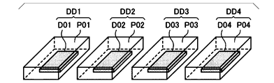
- the semiconductor integrated circuits 1 manufactured by the method for manufacturing the semiconductor integrated circuit according to the first embodiment are individually packaged to form a plurality of semiconductor devices DD1 to DD4. .. Further, based on the interrelationship data shown in FIG. 12 described above, the correspondence between the plurality of packaged semiconductor devices DD1 to DD4 and the unique information represented by the unique circuit 3 of the semiconductor integrated circuit 1 contained therein is established. It produces the second interrelationship data shown.
- FIG. 14A illustrates a step of cutting the substrate 10 on which the semiconductor integrated circuit 1 manufactured by the method for manufacturing the semiconductor integrated circuit of the first embodiment is formed for each semiconductor integrated circuit 1.
- FIG. 14A shows a state in which the five semiconductor integrated circuits 1 arranged in the column C1 are cut (individualized) from the substrate 10.
- the individualized semiconductor integrated circuits 1 are also referred to as semiconductor chips D01 to D05, respectively.
- each of the fragmented semiconductor chips D01 to D04 is packaged by the packaging members P01 to P04 to complete the semiconductor devices DD1 to DD4. Any method may be used for packaging the semiconductor chips D01 to D04.
- the semiconductor integrated circuit 1 of the substrate 10 includes the substrate number W of the substrate and the arrangement position (column) C in the Y direction on the substrate 10.
- a control number IC (W, C, R) is assigned according to the arrangement position (row) R in the X direction.
- the characteristics of each semiconductor integrated circuit 1 defined by the control number IC (W, C, R) are defined by the interrelationship data (INTERRELATIONSHIP DATA) shown in FIG.
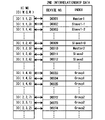
- FIG. 15 is a diagram showing an example of this second interrelationship data (2ND INTERRELATION SHIP DATA).
- the second interrelationship data includes the device numbers (DEVICE NO.) Of the plurality of semiconductor devices DD1 to DD4 and the unique information represented by the unique circuit 3 of the semiconductor integrated circuit 1 included in the semiconductor devices DD1 to DD4 of the device numbers.
- the correspondence with the corresponding code (INDEX) is also 0.
- the control number (IC N0.) Shown at the left end of FIG. 15 is a control number assigned to each semiconductor integrated circuit 1 on the substrate 10 in the interrelationship data shown in FIG.
- the second interrelationship data includes the control number (IC N0.) Of the semiconductor integrated circuit 1 in the interrelationship data shown in FIG. 12 including the semiconductor integrated circuit 1.
- the semiconductor devices DD1 to DD4 may be replaced with the device numbers D0001, D0002 and the like.
- the code (INDEX) in the second interrelationship data may be the same as the code in the interrelationship data shown in FIG.
- the reference numeral in the second interrelationship data may have the same meaning as the reference numeral in the interrelationship data shown in FIG. 12, but may have a different reference numeral.
- the sign in the interrelationship data is "Master1”
- the sign in the second interrelationship data may be "M1".
- the device number D0001 is formed on the surface of the packaging members P01 to P04 or on the surface of the semiconductor integrated circuit 1 not covered by the packaging members P01 to P04. , D0002 and the like may be engraved.
- the second interrelationship data is transferred to the purchaser together with the semiconductor devices DD1 to DD4.
- the user who uses the semiconductor devices DD1 to DD4 selects the semiconductor devices DD1 to DD4 suitable for the purpose of use from the plurality of semiconductor devices DD1 to DD4 based on the second interrelationship data transferred from the manufacturer. And use it. Therefore, it is possible to easily manage a plurality of semiconductor devices DD1 to DD4.
- each of the plurality of semiconductor integrated circuits 1 manufactured by the method for manufacturing the semiconductor integrated circuit of the first embodiment described above is packaged.
- the plurality of semiconductor devices DD1 to DD4 are set, the plurality of semiconductor devices DD1 to DD4 packaged based on the interrelationship data, and the unique circuit 3 of the semiconductor integrated circuit 1 included in the plurality of semiconductor devices DD1 to DD4. It comprises generating a second interrelationship data indicating a correspondence with the unique information represented by.
- DD1 to DD4 Semiconductor device, 1: Semiconductor integrated circuit, 2: Common circuit, 3: Unique circuit, 10: Board, 11: Region, 21: Unique information storage circuit, 22: Encryption circuit, 23: Decoding circuit, 24: Communication circuit, 25: Partial area, 26, 27: Photosensitive film, TR: MOS transistor, Ch0, Ch1: Channel part, SD: Source / drain area, 30: Fixed mask, 31: Mask substrate, 32: Mask pattern , 35: light / dark pattern, SL: selection line, 50: variable shaping exposure device (exposure device), 54: variable shaping mask, 56: substrate holding section, 60: control section, 61: pattern determination section, 62: interrelationship data Generation unit, 63: Storage unit, 70: External server
Landscapes
- Physics & Mathematics (AREA)
- General Physics & Mathematics (AREA)
- Exposure And Positioning Against Photoresist Photosensitive Materials (AREA)
- Exposure Of Semiconductors, Excluding Electron Or Ion Beam Exposure (AREA)
Abstract
基板上の複数の領域のそれぞれに半導体集積回路を製造する製造方法において、マスク基板に固定されたマスクパターンを用いて、複数の領域のそれぞれに、半導体集積回路の一部としての電子回路を形成すること、可変整形マスクを有する可変整形露光装置を用いて、複数の領域のそれぞれの一部に、それぞれの半導体集積回路に固有の固有情報を表す固有回路を形成すること、を備え、複数の領域のそれぞれに形成される固有回路は互いに異なる。
Description
本発明は、半導体集積回路の製造方法、半導体デバイスの製造方法、および露光装置に関する。
本願は、2020年12月25日に出願された日本国特願2020-217784号に基づき優先権を主張し、その内容をここに援用する。
本願は、2020年12月25日に出願された日本国特願2020-217784号に基づき優先権を主張し、その内容をここに援用する。
通信用途に使用される半導体デバイスにおいて、大部分が共通する回路を有する複数の半導体集積回路のそれぞれに、部分的に固有の情報を記憶した固有の回路を形成することにより、通信の守秘性を向上させる半導体集積回路が提案されている(非特許文献1)。
Isabelle Servin、他10名、「Process development of a maskless N40 via level for security application with multi-beam lithography」、SPIE Proceedings Vol. 10584、SPIE(米国)、2018年3月19日
第1の態様によると、半導体集積回路の製造方法は、基板上の複数の領域のそれぞれに半導体集積回路を製造する製造方法において、マスク基板に固定されたマスクパターンを用いて、前記複数の領域のそれぞれに、前記半導体集積回路の一部としての電子回路を形成すること、可変整形マスクを有する可変整形露光装置を用いて、前記複数の領域のそれぞれの一部に、それぞれの前記半導体集積回路に固有の固有情報を表す固有回路を形成すること、を備え、前記複数の領域のそれぞれに形成される前記固有回路は互いに異なる。
第2の態様によると、半導体デバイスの製造方法は、第1の態様による半導体集積回路の製造方法で製造された複数の半導体集積回路を、それぞれパッケージングして複数の半導体デバイスとすること、前記相互関係データに基づいて、パッケージングした複数の前記半導体デバイスと、複数の前記半導体デバイスに含まれる前記半導体集積回路の前記固有回路が表す前記固有情報との対応関係を示す第2の相互関係データを生成すること、を備える。
第3の態様によると、露光装置は、基板を保持する基板保持部と、前記基板上に照射する明暗パターンの形状を設定する可変整形マスクと、前記基板上に形成する複数の半導体集積回路に対応する複数の領域のそれぞれに露光する前記明暗パターンの形状を、複数の前記半導体集積回路の相互間の関係を示す相互関係データに基づいて決定するパターン決定部と、を備える。
第4の態様によると、露光装置は、基板を保持する基板保持部と、前記基板上に照射する明暗パターンの形状を設定する可変整形マスクと、前記基板上に形成する複数の半導体集積回路に対応する複数の所定領域のそれぞれに露光する前記明暗パターンの形状を、複数の前記半導体集積回路のそれぞれに形成すべき、複数ビットのデジタル情報からなる固有情報に基づいて決定するパターン決定部と、を備える。
(第1実施形態の半導体集積回路の製造方法)
図1は、第1実施形態の半導体集積回路の製造方法により基板10上に製造された複数の半導体集積回路1を模式的に示す図である。
図1は、第1実施形態の半導体集積回路の製造方法により基板10上に製造された複数の半導体集積回路1を模式的に示す図である。
図1および以下で参照する各図に矢印で示したX方向、Y方向およびZ方向はそれぞれ直交する方向であるとともに、X方向、Y方向およびZ方向のそれぞれは各図において同一の方向を示している。以下では、各矢印の示す方向を、それぞれ+X方向、+Y方向および+Z方向と呼ぶ。また、X方向の位置をX位置、Y方向の位置をY位置、Z方向の位置をZ位置と呼ぶ。
第1実施形態の半導体集積回路1の製造方法は、一例としてシリコンから成る基板10上の複数の領域11のそれぞれに半導体集積回路1を製造するものである。基板10上に形成された複数の半導体集積回路1は、それぞれの半導体集積回路1に共通する電子回路である共通回路2と、それぞれの半導体集積回路1に固有の固有情報を表す固有回路3とが形成されている。換言すれば、それぞれの半導体集積回路1は、共通回路2と固有回路3とを含むものである。
図1に示したとおり、半導体集積回路1のXY面内での形状は一例として長方形であり、複数の半導体集積回路1は、基板10上で、X方向およびY方向に沿って2次元的に配置されて形成されている。以下では、X方向の配列位置をロウ(R1~R7)、Y方向の配列位置をコラム(C1~R6)として、それぞれの半導体集積回路1をその配列位置に従って識別する場合がある。
図2は、第1実施形態の半導体集積回路の製造方法により製造された半導体集積回路1の1つを拡大して示す図である。半導体集積回路1のうち、上述した共通回路2の部分には、後述する暗号化回路22、復号化回路23、通信回路24を含む種々の回路が形成されている。固有情報記憶回路21は、その一部が共通回路2に含まれ、他の部分は破線で示した固有回路3に含まれている。
図3は、固有情報記憶回路21の一例の回路図を示す図である。固有情報記憶回路21は、一例として、一般的なNAND型のマスクROM回路であり、Y方向に延びるデータ線DLに沿って複数のMOSトランジスタTRが配置され、各MOSトランジスタTRのゲートに、X方向に延びる選択線SLが接続されている。各データ線DLの両端には、それぞれ電圧印加部26と電圧検知部27が配置されている。各選択線SLの端部には、選択線SLを介して各MOSトランジスタTRのゲートに電圧を印加する電圧印加部28が配置されている。
固有情報記憶回路21のうち、マスクROM回路の記憶領域を構成する複数のMOSトランジスタTRは、破線で示した固有回路3に含まれている。一方、電圧印加部26,28、および電圧検知部27は固有回路3には含まれず、図2に示した共通回路2に含まれている。
なお、上述したとおり、固有情報記憶回路21は、その構成自体は一般的なマスクROM回路であるため、その詳細の説明は省略する。
なお、本明細書において、回路とは、1つの機能を発揮する完成した電気回路のみではなく、ある程度完成している電気回路の一部分をも含む。
なお、上述したとおり、固有情報記憶回路21は、その構成自体は一般的なマスクROM回路であるため、その詳細の説明は省略する。
なお、本明細書において、回路とは、1つの機能を発揮する完成した電気回路のみではなく、ある程度完成している電気回路の一部分をも含む。
図4Aは、マスクROM回路である固有回路3のうちの、図3に破線で囲って示した部分領域25の構造を、+Z方向から見た上面図を示している。図4Bは、図4A中のAA線に沿った部分の断面を示す図である。
固有回路3の内部には、ソース/ドレイン領域SDと、選択線SLであるゲート電極と、ゲート酸化膜GOと、チャネル部Ch0,Ch1とからなる、一例としてn型のMOSトランジスタTR(TR1、TR2)が複数形成されている。ソース/ドレイン領域SDは、一例としてリンやヒ素である不純物イオンが高濃度でドーピングされている。
固有回路3の内部には、ソース/ドレイン領域SDと、選択線SLであるゲート電極と、ゲート酸化膜GOと、チャネル部Ch0,Ch1とからなる、一例としてn型のMOSトランジスタTR(TR1、TR2)が複数形成されている。ソース/ドレイン領域SDは、一例としてリンやヒ素である不純物イオンが高濃度でドーピングされている。
同じX位置に配置され、Y方向に並ぶ複数のMOSトランジスタTR1、TR2のそれぞれのソース/ドレイン領域SDは、Y方向にそれぞれ連続して形成されている。これにより、複数のMOSトランジスタTR1、TR2のソース/ドレイン領域SD、およびチャネル部Ch0,Ch1は、全体として、データ線DL(図3参照)を形成している。
MOSトランジスタTR1等のいくつかのMOSトランジスタのチャネル部Ch0は、不純物イオンの濃度が低い真性半導体状態とされている。一方、MOSトランジスタTR2等のいくつかのMOSトランジスタのチャネル部Ch1は、一例としてリンやヒ素である不純物イオンの濃度が高いn型半導体状態とされている。
不純物イオンの濃度が高いチャネル部Ch1を有するMOSトランジスタTR2は、ゲートである選択線SLに正または0[V]のいずれの電位が印加された状態であっても導通する。よって、MOSトランジスタTR2に含まれるチャネル部Ch1は、例えばデータ「1」に相当する状態が記憶されている。
一方、不純物イオンの濃度が低いチャネル部Ch0を有するMOSトランジスタTR1は、ゲートである選択線SLに正の電位が印加された状態に限り導通する。よって、MOSトランジスタTR1に含まれるチャネル部Ch0は、例えばデータ「0」に相当する状態が記憶されている。
なお、不純物イオンの濃度が低いチャネル部Ch0が記憶するデータを「1」とし、不純物イオンの濃度が高いチャネル部Ch1が記憶するデータを「0」としても良い。
なお、不純物イオンの濃度が低いチャネル部Ch0が記憶するデータを「1」とし、不純物イオンの濃度が高いチャネル部Ch1が記憶するデータを「0」としても良い。
基板10上に形成される複数の半導体集積回路1は、それぞれ上述した共通回路2と固有回路3とを含んでいる。そして、固有回路3のうちの一部、例えば上述したチャネル部Ch0、Ch1の不純物イオンの濃度の分布は、複数の半導体集積回路1のそれぞれで異なっている。
第1実施形態の製造方法においては、半導体集積回路1のうち、固有回路3のうち複数の半導体集積回路1に共通する回路部分および共通回路2については、マスク基板に固定されたマスクパターン(以降、マスク基板とマスクパターンとを合わせて「固定マスク」とも呼ぶ)を用いる露光により形成する。固定マスクは、一例として、透光性のマスク基板にマスクパターンとしてクロム等の遮光膜、または位相シフターとしての誘電体の透過膜が形成された透光型のマスクであっても良い。あるいは、反射性のマスク基板の表面にマスクパターンとして吸光性の膜、または位相シフターとしての段差形状が形成された反射型のマスクであっても良い。
一方、固有回路3のうち複数の半導体集積回路1のそれぞれで異なる回路部分については、可変整形マスクを用いる露光により形成する。可変整形マスクは、いわゆる空間光変調器である。反射型の可変整形マスクとしては、例えば、反射面に複数の可動微小ミラーが形成されたものや、反射型の液晶表示デバイスを用いることができる。透過型の可変整形マスクとしては、例えば、透過型の液晶表示デバイスを用いることができる。なお、可変整形マスクを用いる露光装置の詳細については、後述する。
以下、図6を参照して第1実施形態の製造方法のフローを説明する。
一般的な半導体集積回路の製造と同様に、第1実施形態の製造方法においても、基板10に対して、複数回のリソグラフィ工程を行うことにより、半導体集積回路1を製造する。従って、ステップS100は、全部でN回のリソグラフィ工程を含むループの開始にあたるステップである。
なお、基板10は、1枚の基板には限らず、複数の基板の集合体であっても良い。
一般的な半導体集積回路の製造と同様に、第1実施形態の製造方法においても、基板10に対して、複数回のリソグラフィ工程を行うことにより、半導体集積回路1を製造する。従って、ステップS100は、全部でN回のリソグラフィ工程を含むループの開始にあたるステップである。
なお、基板10は、1枚の基板には限らず、複数の基板の集合体であっても良い。
なお、本明細書においては、リソグラフィ工程とは、基板10上に感光膜(レジスト)を形成し、露光および現像により感光膜をパターニングし、パターニングした感光膜を用いて基板10を加工する一連の工程をいう。リソグラフィ工程には、感光膜の形成前に基板10上に所定の膜を形成する工程を含んでも良い。また、基板10の加工は、基板10または基板10上に形成した所定の膜に対するエッチング、酸化、窒化、またはイオン注入であっても良い。
ステップS110では、j回目のリソグラフィ工程は、可変整形マスクを用いた露光を行う工程であるか否かを判断する。判断が否定された(No)場合、ステップS120に進み、固定マスクを用いた露光を含むリソグラフィ工程を行う。ステップS120においては、半導体集積回路1の暗号化回路22、復号化回路23、通信回路24を含む共通回路2を構成する回路パターンが形成された固定マスクを使用する。従って、ステップS120においては、基板10上に暗号化回路22、復号化回路23、通信回路24を含む共通回路2の一部を構成する回路パターンが形成される。
固定マスクを用いた露光を含むリソグラフィ工程は、半導体集積回路の製造のために通常用いられているリソグラフィ工程と同様であるので、その詳細な説明は省略する。
固定マスクを用いた露光を含むリソグラフィ工程は、半導体集積回路の製造のために通常用いられているリソグラフィ工程と同様であるので、その詳細な説明は省略する。
なお、ステップS120で使用する固定マスクは、固有回路3のうち複数の半導体集積回路1に共通する部分の回路パターンに相当するマスクパターンを含んでいても良い。この場合には、ステップS120においては、基板10上に、上述した各種の回路パターンに加えて、固有回路3のうち複数の半導体集積回路1に共通する部分の回路パターンの一部も併せて形成される。
ステップS120において、固有回路3のうち複数の半導体集積回路1に共通する部分の回路パターンを形成する方法を、図7A、図7Bを参照して説明する。図7Aは、複数の半導体集積回路1に共通する部分の回路パターンを形成するための、固定マスク30の一例を示す図である。固定マスク30は、透光性のマスク基板31と、マスク基板31の表面に形成された、一例として固有情報記憶回路21内のソース/ドレイン領域SDを形成するためのマスクパターン32とを含む。マスクパターン32は、透光部33と遮光部34とを含む。
なお、図7Aは、固有情報記憶回路21内のソース/ドレイン領域SDのうちの図3および図5に示した部分領域25に相当する部分25Mに対応するマスクパターン32を示している。図7Aの中のAA線は、図5に示したAA線に対応するマスクパターン32上の位置に示してある。なお、マスクパターン32は、固有情報記憶回路21の部分領域25以外の部分、および暗号化回路22、復号化回路23、通信回路24等の他の回路に相当するマスクパターンを含んでいても良い。あるいは、マスクパターン32は、固有情報記憶回路21の部分領域25内のパターンを含まず、暗号化回路22、復号化回路23、通信回路24等の他の回路に相当するマスクパターンのみを含んでいても良い。
図7Bは、図7Aに示した固定マスク30を用いて、基板10上の各領域11内の固有回路3に相当する部分にソース/ドレイン領域SDを形成する工程を示す図である。図7Bは、図5に示したAA線における基板10の断面図である。
始めに、基板10上にフォトレジスト等の感光膜26を形成し、感光膜26に対し、固定マスク30を用いて露光を行い、透光部33に相当する部分の感光膜26を感光させる。そして感光膜26のうち感光した部分を現像により除去して開口部26oを形成し、開口部26oから基板10の表面を露出させる。
その後、残存している感光膜26、すなわちパターニングされた感光膜26をマスクとして、基板10に対して一例としてヒ素またはリンをイオン注入して、ソース/ドレイン領域SDを形成する。
なお、これと同時に、固有情報記憶回路21の部分領域25以外の部分、および暗号化回路22、復号化回路23、通信回路24等の他の回路の中の所定の部分に、ソース/ドレイン領域を形成しても良い。
なお、これと同時に、固有情報記憶回路21の部分領域25以外の部分、および暗号化回路22、復号化回路23、通信回路24等の他の回路の中の所定の部分に、ソース/ドレイン領域を形成しても良い。
ステップS120の工程の終了後は、ステップS160に進み、N回のプロセスが終了するまで、ステップS110からステップS160までのループを繰り返す。
ステップS110での判断が肯定された(Yes)場合、ステップS130に進む。ステップS130では、j回目のリソグラフィ工程は、可変整形マスクを用いた露光に加えて、固定マスクを用いた露光も行う工程であるか否かを判断する。判断が否定された(No)場合、ステップS140に進み、可変整形マスクを用いた露光を含むリソグラフィ工程を行う。
ステップS140においては、固有情報記憶回路21の固有回路3について複数の半導体集積回路1でそれぞれ異なる回路パターンを形成する。ただし、図12を参照して後述するように一部の半導体集積回路1については、固有回路3に同じパターンを形成しても良い。
図8Aは、可変整形マスクを用いて基板10上に形成する明暗パターン35の形状(明暗分布)を示す図である。図8Aの中のAA線は、図5に示したAA線に対応する位置に示してある。図8Aには、明暗パターン35のうち、部分領域25に相当する小領域25E内のパターンのみを示しているが、明暗パターン35は、固有回路3の全てに対応するエリアを有していても良い。
図8Bは、図8Aに示した明暗パターン35を用いて、固有回路3に含まれる複数のMOSトランジスタTRのチャネル部Ch0、Ch1のそれぞれに所定の不純物濃度のイオンを注入する方法を説明する図である。図8Bは、図5に示したAA線における基板10の断面図である。
ステップS140においては、基板10上にフォトレジスト等の感光膜27を形成し、感光膜27に対し、可変整形マスクにより形成された明暗パターン35を露光する。このとき、チャネル部Ch1に相当する部分が明部36となり、他の部分は、暗部37となるように、明暗パターン35の形状(明暗分布)を設定する。すなわち、チャネル部Ch0に相当する部分38は、チャネル部Ch0およびチャネル部Ch1以外に相当する部分39と同じく暗部37となるように可変整形マスクを設定する。この明暗パターン35は、基板10内のそれぞれ領域11に形成される半導体集積回路1ごとに、それぞれ異ならせることができる。
明部36により露光された部分の感光膜27は、その後の現像により除去されて開口部27oとなり、開口部27oから基板10の表面が露出する。その後、残存している感光膜27、すなわちパターニングされた感光膜27をマスクとして、基板10に対して一例としてヒ素またはリンをイオン注入して、チャネル部Ch1に所定の濃度の不純物イオンを注入する。
このとき、チャネル部Ch0に相当する部分は、感光膜27で覆われているためイオンは注入されない。従って、ステップS140により、固有情報記憶回路21の一例としてのNAND型マスクROMを構成する複数のMOSトランジスタのそれぞれのチャネル部に、所定の不純物イオンの濃度の分布を形成することができる。上述したように、例えば不純物イオンが高濃度でドーピングされたチャネル部Ch1には1ビットのデータ「1」が記憶され、不純物イオンがドーピングされていない(低濃度の)チャネル部Ch0には1ビットのデータ「0」が記憶される。従って、固有回路3の中に、それぞれチャネル部を有するM個のMOSトランジスタTRがあれば、固有回路3にMビットの情報を記憶させることができる。固有回路3に含まれるMOSトランジスタTRの数は、図3に示した8×8=64個に限られるわけではなく、任意の個数であって良い。
これにより、基板10上の複数の領域11にそれぞれ形成される半導体集積回路1のそれぞれの固有情報記憶回路21に、それぞれ異なる固有情報を記憶させることができる。換言すれば、基板10上の複数の領域11のそれぞれの一部に、それぞれの半導体集積回路1に固有の固有情報を表し、かつ、それぞれの回路パターンの少なくとも一部が異なる固有回路3を形成することができる。なお、上述したチャネル部Ch0、Ch1の不純物イオンの濃度の分布も、回路パターンであるということができる。
ステップS140の工程の終了後は、ステップS160に進み、N回のプロセスが終了するまで、ステップS110からステップS160までのループを繰り返す。
ステップS130での判断が肯定された(Yes)場合には、ステップS150に進む。
図9、図10A、図10B、図10Cは、ステップS150におけるリソグラフィ工程を説明する図であり、ステップS150は、固定マスクを用いた露光に加えて、可変整形マスクを用いた露光も行うリソグラフィ工程である。
図9、図10A、図10B、図10Cは、ステップS150におけるリソグラフィ工程を説明する図であり、ステップS150は、固定マスクを用いた露光に加えて、可変整形マスクを用いた露光も行うリソグラフィ工程である。
ステップS150においては、図9のフローに示したように、始めにステップS151において基板10上に薄膜を形成する。なお、薄膜の形成が不要である場合には、ステップS151を省略しても良い。
続いて、ステップS152において基板10上にフォトレジスト等の感光膜26を形成する。そして、ステップS153において、図7Aに示したような固定マスク30を用いて、感光膜26を露光する。固定マスク30を用いた露光を行った後の基板10および感光膜26の断面図を、図10Aに示す。なお、図10Aは、図7Bおよび図8Bと同様に、図5のAA線における基板10の断面図である。
固定マスク30を用いた露光により、感光膜26には感光部26Eが形成される。固定マスク30を用いた露光により感光しなかった部分は、非感光部26Nとして残存する。
固定マスク30を用いた露光により、感光膜26には感光部26Eが形成される。固定マスク30を用いた露光により感光しなかった部分は、非感光部26Nとして残存する。
続いて、ステップS154において、感光膜26を現像する。現像後の感光膜26は、図7Bに示した感光膜26と同様の状態となる。
その後、ステップS155において、残存する感光膜26に対し、可変整形マスクにより形成された、図8Aに示したごとき明暗パターン35を露光する。そして、ステップS156において、感光膜26を再度、現像する。現像後の感光膜26は、図10Cに示したとおり、ステップS153における固定マスク30を用いた露光、およびステップS155における可変整形マスクを用いた露光のいずれでも感光しなかった非感光部26Nだけが基板10上に残存する。
その後、ステップS155において、残存する感光膜26に対し、可変整形マスクにより形成された、図8Aに示したごとき明暗パターン35を露光する。そして、ステップS156において、感光膜26を再度、現像する。現像後の感光膜26は、図10Cに示したとおり、ステップS153における固定マスク30を用いた露光、およびステップS155における可変整形マスクを用いた露光のいずれでも感光しなかった非感光部26Nだけが基板10上に残存する。
この状態で、ステップS157に進み、図10Cに示した非感光部26Nが残存する感光膜26、すなわちパターンニングされた感光膜26を用いて、基板10に対する処理を行う。図10Cに示した例では、基板10に対する処理とは、一例として基板10に対するヒ素またはリンのイオン注入であり、このイオン注入により、ソース/ドレイン領域SD、およびチャネル部Ch1が、同時に形成される。一方、チャネル部Ch0は、感光膜26により覆われているので、イオン注入は行われない。
なお、ステップS151において、基板10上に薄膜を形成している場合には、イオン注入は、基板10にではなく、基板10上に形成された薄膜に対して行っても良い。
なお、上述の工程においては、固定マスクを用いた露光の後と、可変整形マスクを用いた露光の後とのそれぞれで感光膜26の現像を行ったが、固定マスクを用いた露光の後の現像(ステップS154の現像)は省略しても良い。この場合、ステップS155の実行後の感光膜26には、図10Bに示した断面図のように、固定マスク30を用いた露光による感光部26Eと、可変整形マスクを用いた露光による感光部26Fと、いずれの露光でも感光しなかった非感光部26Nとが形成される。この状態の感光膜26を、ステップS156において現像することにより、図10Cに示した状態の感光膜26(非感光部26N)を形成しても良い。また、上述の工程においては、固定マスクを用いた露光の後に、可変整形マスクを用いた露光を行ったが、可変整形マスクを用いた露光の後に、固定マスクを用いた露光を行ってもよい。
以上より、ステップS150においても、上述したステップS140と同様に、可変整形マスクを用いて、基板10上の複数の領域11のそれぞれの一部に、それぞれの半導体集積回路1に固有の固有情報を表し、かつ、それぞれの回路パターンの少なくとも一部が異なる固有回路3を形成することができる。
ステップS150の工程の終了後は、ステップS160に進み、N回のプロセスが終了するまで、ステップS110からステップS160までのループを繰り返す。
なお、ステップS160の終了後に、後述するように、基板10から個々の半導体集積回路1を切断(個片化)しても良い。
なお、ステップS160の終了後に、後述するように、基板10から個々の半導体集積回路1を切断(個片化)しても良い。
図4A、図4Bに示したように、イオン注入されたチャネル部Ch1およびイオン注入されていないチャネル部Ch0の上には、その後の工程で、ゲートとしての選択線SLが形成される。従って、完成した半導体集積回路1を上面から観察等しただけでは、各チャネル部Ch0、Ch1の不純物イオンの濃度を解析することは困難である。よって、上述した方法においては、固有回路3に記憶された固有情報がリバースエンジニアリングされる恐れを低減することができる。
なお、ステップS120、ステップS140、およびステップS150のいずれにおいても、パターンニングされた感光膜26、27を用いての基板10の加工は、上述したイオン注入に限られるわけではない。すなわち、基板10の加工は、基板10または基板10上に形成した所定の膜に対するエッチング、酸化、窒化等の他の加工であっても良い。また、基板10または基板10上に形成した所定の膜に所定のエッチングを行なうことで溝またはホールを形成した後に、その溝またはホールに金属等の導電体を部分的に埋め込むものであっても良い。
また、ステップS120、およびステップS140においても、ステップS150と同様に、基板10への感光膜26、27の形成前に基板10上に所定の膜を形成する工程を含んでも良い。
また、固定マスク30を用いた露光または可変整形マスクを用いた露光の後であって、現像の前に、感光膜26、27を加熱するPEB処理を含んでいても良い。
また、固定マスク30を用いた露光または可変整形マスクを用いた露光の後であって、現像の前に、感光膜26、27を加熱するPEB処理を含んでいても良い。
なお、それぞれの半導体集積回路1に固有の固有情報を表し、かつ、それぞれの回路パターンの少なくとも一部が異なる固有回路3、および固有回路3を含む固有情報記憶回路21は、上述したNAND型マスクROMに限られるわけではない。従って、固有回路3の中のそれぞれの半導体集積回路1に固有のパターンについても、上述した不純物イオンの濃度分布に限られるわけではない。
固有回路3の中の半導体集積回路1に固有のパターンは、電子素子を構成する回路の中の特定のトランジスタの有無、ゲート長の差、またはゲート幅の差等であっても良い。あるいは、電子素子を構成する回路の中の特定のビアホール等の接続部の有無またはサイズの差であっても良い。そして、これらの有無やサイズの差により生じる電子素子の動作特性の差によって、信号「1」または信号「0」が記憶される回路であっても良い。
これらのトランジスタまたはビアホール等の形成は、可変整形露光装置を用いた露光を含む2回以上のリソグラフィ工程により行なっても良い。
なお、上述したステップS140およびステップS150では、固有回路3の中の半導体集積回路1に固有の固有情報を表す固有パターンであるチャネル部Ch0、Ch1の形成を、可変整形露光装置を用いた露光を含む1回のリソグラフィ工程により行なうことができる。従って、固定マスク30を使用する露光に比べて処理時間が掛かる可変整形露光装置を用いる露光の必要回数を低減することができ、半導体集積回路1の生産性を高めることができる。
なお、上述したステップS140およびステップS150では、固有回路3の中の半導体集積回路1に固有の固有情報を表す固有パターンであるチャネル部Ch0、Ch1の形成を、可変整形露光装置を用いた露光を含む1回のリソグラフィ工程により行なうことができる。従って、固定マスク30を使用する露光に比べて処理時間が掛かる可変整形露光装置を用いる露光の必要回数を低減することができ、半導体集積回路1の生産性を高めることができる。
なお、可変整形露光装置を用いた露光は、上述した紫外線を含む光を用いた露光に限られるものではなく、電子線等の荷電粒子線を用いた露光であっても良い。この場合、可変整形マスクとして、例えば、いわゆるブランキングアパーチャーアレイを用いても良い。
次に、図11を参照して、可変整形マスクを用いて固有回路3を形成するために基板10に明暗パターンを露光する方法の一例を説明する。
図1に示したとおり、複数の半導体集積回路1は、X方向およびY方向に沿って基板10上に2次元的に配置された領域11のそれぞれに形成されている。従って、固有回路3を、それぞれの半導体集積回路1の内部において共通の位置に配置することにより、複数の固有回路3は、X方向およびY方向に沿って2次元的に配置されることになる。
図1に示したとおり、複数の半導体集積回路1は、X方向およびY方向に沿って基板10上に2次元的に配置された領域11のそれぞれに形成されている。従って、固有回路3を、それぞれの半導体集積回路1の内部において共通の位置に配置することにより、複数の固有回路3は、X方向およびY方向に沿って2次元的に配置されることになる。
そこで、可変整形マスクを備えた露光装置を用いて、複数の固有回路3を、図11に示したように、例えばY方向に沿った一度の走査露光により露光しても良い。すなわち、破線で示した走査経路SP1に沿った走査露光により、ロウR1に配置されている複数の領域11の半導体集積回路1に含まれる複数の固有回路3を露光しても良い。同様に、走査経路SP2~SP7に沿ったそれぞれの走査露光により、ロウR2~R7にそれぞれ配置されている複数の領域11の半導体集積回路1に含まれる複数の固有回路3を露光しても良い。
固有回路3のX方向の幅AWは、例えば100μm程度以下で良く、従って、可変整形マスクを備えた露光装置のX方向の露光視野も100μm程度以下で良い。可変整形マスクを備えた露光装置については、図13を参照して後述する。
このような走査露光を行うことにより、それぞれの固有回路3の露光の前後に必要な基板10の加速または減速に必要な時間を削減することができ、従って、露光に必要な処理時間を短縮し、スループットを向上させることができる。
このような走査露光を行うことにより、それぞれの固有回路3の露光の前後に必要な基板10の加速または減速に必要な時間を削減することができ、従って、露光に必要な処理時間を短縮し、スループットを向上させることができる。
なお、図11に示したように、X方向に隣接するそれぞれの走査経路SP1~SP7においては、走査方向(露光時の基板10の移動方向)を相互に反転させることにより、それぞれの走査経路SP1~SP7の間の基板10の移動距離を削減しても良い。これにより、さらにスループットを向上させても良い。
なお、可変整形マスクを備えた露光装置を用いての走査露光は、Y方向に沿ったものに限られることはなく、X方向に沿ったものであっても良い。
Y方向(またはX方向)を第1方向ということができ、X方向(またはY方向)を第1方向であるY方向(またはX方向)と交差する第2方向ということができる。
Y方向(またはX方向)を第1方向ということができ、X方向(またはY方向)を第1方向であるY方向(またはX方向)と交差する第2方向ということができる。
次に、図12を参照して、固有情報の一例として暗号鍵(Cryptographic key)を固有回路3に記憶する例について説明する。暗号鍵は、半導体集積回路1が送信し、または受信する信号を、暗号化回路22で暗号化し、または復号化回路23で復号化する際に使用する暗号鍵である。
暗号鍵として、例えば0x34F23E1A等の4バイトの16進コードの数値を使用する。従って、基板10上のそれぞれの領域11に形成する半導体集積回路1の固有情報記憶回路21の中の固有回路3には、それぞれの領域11に形成する半導体集積回路1の使用目的に応じた値の暗号鍵を記憶させる。
暗号鍵として、例えば0x34F23E1A等の4バイトの16進コードの数値を使用する。従って、基板10上のそれぞれの領域11に形成する半導体集積回路1の固有情報記憶回路21の中の固有回路3には、それぞれの領域11に形成する半導体集積回路1の使用目的に応じた値の暗号鍵を記憶させる。
それぞれの領域11に形成する半導体集積回路1にどの暗号鍵を記憶させるかは、図12に示した、相互関係データ(INTERRELATIONSHIP DATA)に基づいて決定する。相互関係データは、製造する複数の半導体集積回路1のうちの1つと、他の1つまたは複数との相互間の関係を示すデータである。換言すれば、相互関係データは、それぞれの半導体集積回路1が形成されている基板10の基板番号Wと、基板10上でのY方向の配列位置(コラム)Cと、X方向の配列位置(ロウ)Rで特定される半導体集積回路1のそれぞれの、他の半導体集積回路1との関係性を示すデータである。基板番号Wの、すなわちW枚目の基板のコラムC、ロウRの位置に配置される半導体集積回路1には、IC(W,C,R)の管理番号(IC N0.)が付与されている。
一例として相互関係データの中では、管理番号IC(1,1,2)の半導体集積回路1に、1組目の複数の半導体集積回路1の中でマスターチップとなるべき半導体集積回路1であることを示すMaster-1 という符号(INDEX)が割り振られている。これに従って、管理番号IC(1,1,2)の半導体集積回路1の固有情報記憶回路21には、これを1組目の複数の半導体集積回路1の中でマスターチップとして機能させる暗号鍵0x34F23E1Aを記憶させる。
また、管理番号IC(1,1,3)の半導体集積回路1は、1組目の複数の半導体集積回路1の中で1番目のスレーブチップとなるべき半導体集積回路1であることを示すSlave-1-1 という符号が割り振られている。これに従って、管理番号IC(1,1,3)の半導体集積回路1の固有情報記憶回路21には、これを1組目の複数の半導体集積回路1の中で1番目のスレーブチップとして機能させる暗号鍵0xAB56BD23を記憶させる。
同様にして、管理番号IC(1,1,4)の半導体集積回路1には、割り振られたSlave-1-2 という符号に対応して、これを1組目の複数の半導体集積回路1の中で2番目のスレーブチップとして機能させる暗号鍵0x7EA843BCを記憶させる。
他の一例として、管理番号IC(1,2,5)の半導体集積回路1には、割り振られたMaster-2 という符号に対応して、これを2組目の複数の半導体集積回路1の中でマスターチップとして機能させる暗号鍵0x7EA843BCを記憶させる。そして、管理番号IC(1,2,6)および管理番号IC(1,2,7)の半導体集積回路1には、割り振られたSlave-2
という符号に対応して、これを2組目の複数の半導体集積回路1の中でスレーブチップとする同一の暗号鍵0x59C6AF32を記憶させる。
という符号に対応して、これを2組目の複数の半導体集積回路1の中でスレーブチップとする同一の暗号鍵0x59C6AF32を記憶させる。
さらに他の一例として、管理番号IC(1,4,4)、管理番号IC(1,4,5)、および管理番号IC(1,4,6)の半導体集積回路1には、割り振られたGroup-1 という符号に対応して、これをGroup-1という組に属する複数の半導体集積回路1とする共通の暗号鍵0xBA5CFE4Dを記憶させる。
同様にして、2枚目の基板10上に形成する管理番号IC(2,2,7)、管理番号IC(2,3,1)、および管理番号IC(2,3,2)の半導体集積回路1には、割り振られたGroup-2 という符号に対応して、これをGroup-2という組に属する複数の半導体集積回路1とする共通の暗号鍵0xC4A25D3Bを記憶させる。
なお、暗号鍵は、上述した4バイトの16進コードに限られるものではなく、任意のビット数のデジタルデータであって良い。また、暗号鍵自体ではなく、例えば、暗号鍵に対して所定の演算を行った結果得られるデジタルデータであっても良い。暗号鍵自体、および暗号鍵に対して所定の演算を行った結果得られるデジタルデータを、以下では、「暗号鍵に関する情報」ともいう。
第1実施形態の製造方法で製造された複数の半導体集積回路1は、それぞれの固有回路3内に記憶している暗号鍵に関する情報に対応する符号により関係付けられた1つまたは複数の他の半導体集積回路1に対してのみ、暗号化および復号化を伴う通信が可能である。逆に言えば、複数の半導体集積回路1を概ね共通する回路パターンで形成し、固有回路3内の一部の回路パターンをそれぞれ変更することにより、他の特定の1つまたは複数の半導体集積回路1だけとの通信が可能な半導体集積回路1を製造することができる。
なお、固有回路3内に記憶される固有情報は、上述した暗号鍵に限られるものではなく、例えば、それぞれの半導体集積回路1を表す識別情報であっても良い。
なお、固有回路3内に記憶される固有情報は、上述した暗号鍵に限られるものではなく、例えば、それぞれの半導体集積回路1を表す識別情報であっても良い。
固有回路3内に記憶される暗号鍵等の固有情報を、第1実施形態の半導体集積回路1の製造方法を実施する半導体製造者が決定しても良い。さらには、固有情報と相互関係データに含まれるそれぞれの符号との対応関係についても、半導体製造者が決定しても良い。あるいは、半導体製造者に半導体集積回路1の製造を委託する委託者が、上記の固有情報について、またはそれぞれの固有情報と符号との対応関係について決定しても良い。
固有情報と相互関係データに含まれる符号との対応関係を、または固有情報を半導体製造者が決定する場合、半導体集積回路1に実際に記憶された固有情報は、半導体製造者のみが把握することになる。従って、この場合には、固有情報に関する情報は半導体製造者以外の者に知られることがないため、暗号鍵等の固有情報に関する秘密性を高度に維持することができる。
また、後述するように、固有情報と相互関係データに含まれる符号との対応関係を、または固有情報を、後述するように可変整形マスクを用いた露光において使用する可変整形露光装置が決定(生成)しても良い。この場合には、半導体集積回路1に実際に記憶された固有情報は、可変整形露光装置のみが把握し、それ以外の者には知り得ない情報となる。従って、この場合には、固有情報に関する秘密性を一層高度に維持することができる。
相互関係データについても、第1実施形態の半導体集積回路1の製造方法を実施する半導体製造者が生成しても良く、または、後述するように可変整形マスクを用いた露光において使用する可変整形露光装置が生成しても良い。あるいは、相互関係データは、半導体製造者に半導体集積回路1の製造を委託する委託者が決定しても良い。
相互関係データを半導体製造者が生成する場合、または可変整形露光装置が生成する場合には、製造した複数の半導体集積回路1とともに、相互関係データを半導体集積回路1の使用者(半導体集積回路1の製造を委託した者)に譲渡すると良い。半導体集積回路1を使用する使用者は、製造者から譲渡された相互関係データに基づいて、複数の半導体集積回路1の中から使用目的に合致する半導体集積回路1を選択して使用すれば良い。
(第1実施形態の半導体集積回路の製造方法の効果)
(1)以上で説明した第1実施形態の半導体集積回路1の製造方法は、基板10上の複数の領域11のそれぞれに半導体集積回路1を製造する製造方法において、マスク基板31に固定されたマスクパターン32を用いて、複数の領域11のそれぞれに、半導体集積回路1の一部としての電子回路(共通回路2)を形成すること、可変整形マスクを有する可変整形露光装置を用いて、複数の領域11のそれぞれの一部に、それぞれの半導体集積回路1に固有の固有情報を表す固有回路3を形成すること、を備え、複数の領域11のそれぞれに形成される固有回路3は互いに異なる。
この構成により、それぞれが固有の固有回路3を有する複数の半導体集積回路1を安価に製造することができる。
(2)共通回路2である電子回路は、情報を暗号化または復号化する回路の少なくとも一部(暗号化回路22、復号化回路23)を含み、固有情報は、情報を暗号化または復号化する際に用いる暗号鍵に関する情報であっても良い。
この構成により、複数の半導体集積回路1を概ね共通する回路パターンで形成し、固有回路3内の一部の回路パターンをそれぞれ変更することにより、他の特定の1つまたは複数の半導体集積回路1だけとの通信が可能な半導体集積回路1を製造することができる。
この構成により、複数の半導体集積回路1を概ね共通する回路パターンで形成し、固有回路3内の一部の回路パターンをそれぞれ変更することにより、他の特定の1つまたは複数の半導体集積回路1だけとの通信が可能な半導体集積回路1を製造することができる。
(3)基板10上の第1方向、および前記第1方向と交差する第2方向に沿って配置される複数の前記領域のそれぞれに電子回路(共通回路2)を形成し、固有回路3の形成は、感光膜26を形成した基板10を可変整形露光装置に対して第1方向(Y方向)に沿って相対的に走査させ、走査中に複数の複数の領域11のうちの第1方向(Y方向)に沿って配置される複数の領域11に対して露光を行うことを含むものであっても良い。
この構成により、固有回路3の形成をより短時間で行うことができ、半導体集積回路1の生産性をより高めることができる。
この構成により、固有回路3の形成をより短時間で行うことができ、半導体集積回路1の生産性をより高めることができる。
(4)固有回路3の中にあり、半導体集積回路1に固有の固有情報を表す固有パターン(チャネル部Ch0、Ch1)の形成は、可変整形露光装置を用いた露光を含む1回のリソグラフィ工程により行っても良い。これにより、可変整形露光装置を用いる露光の回数を低減することができ、半導体集積回路1の生産性を一層高めることができる。
(5)電子回路(共通回路2)はNAND型マスクROM(固有情報記憶回路21)を含み、固有回路3は、NAND型マスクROMを構成する複数のMOSトランジスタTRのそれぞれのチャネル部Ch0、Ch1に注入された不純物イオンの濃度分布を含むものであっても良い。この構成により、可変整形露光装置を用いる露光の回数を低減することができ、半導体集積回路1の生産性を一層高めることができる。
(5)電子回路(共通回路2)はNAND型マスクROM(固有情報記憶回路21)を含み、固有回路3は、NAND型マスクROMを構成する複数のMOSトランジスタTRのそれぞれのチャネル部Ch0、Ch1に注入された不純物イオンの濃度分布を含むものであっても良い。この構成により、可変整形露光装置を用いる露光の回数を低減することができ、半導体集積回路1の生産性を一層高めることができる。
(第2実施形態の露光装置)
図13は、第2実施形態の露光装置50の構成を概略的に示す図である。第2実施形態の露光装置50は、可変整形マスク54を備え、基板10上に、形状可変の明暗パターン35を露光する可変整形露光装置である。可変整形マスク54は、上述した空間光変調器の中のいずれか1つで良いが、本実施形態では、可変マスク面DPに複数の微小反射面が配置された反射型の空間光変調器を採用している。露光装置50は、さらに送光光学系52、分岐素子53、結像光学系55、基板保持部56、定盤57、および制御部60等を備えている。
図13は、第2実施形態の露光装置50の構成を概略的に示す図である。第2実施形態の露光装置50は、可変整形マスク54を備え、基板10上に、形状可変の明暗パターン35を露光する可変整形露光装置である。可変整形マスク54は、上述した空間光変調器の中のいずれか1つで良いが、本実施形態では、可変マスク面DPに複数の微小反射面が配置された反射型の空間光変調器を採用している。露光装置50は、さらに送光光学系52、分岐素子53、結像光学系55、基板保持部56、定盤57、および制御部60等を備えている。
基板10は定盤57上に配置されている基板保持部56上に載置される。基板10は基板保持部56により定盤57上をX方向およびY方向に移動可能である。また、基板10は、基板保持部56によりZ方向にも微小距離だけ移動可能であり、さらにX方向およびY方向を回転軸として微小角度だけ回転(チルト)可能である。
基板10のX方向およびY方向の位置は、基板保持部56に設けられているスケール板58の位置を介して位置計測部59により計測され、計測信号S3として制御部60に伝達される。制御部60は、計測信号S3に基づいて基板保持部56に位置制御信号S4を送り、基板10が所定のX位置およびY位置に配置されるように制御する。
制御部60は、光源51に対して露光制御信号S2を送り、光源51の発光タイミングおよび発光量を制御する。
制御部60は、光源51に対して露光制御信号S2を送り、光源51の発光タイミングおよび発光量を制御する。
露光装置50は、基板10および基板保持部56を、投影光学系55に対してXY面内方向に相対的に走査しながら露光を行う走査型の露光装置であっても良い。この場合には、露光装置50は、図11に示した走査経路SP1~SP7に沿った走査露光を行うことにより、基板10の露光に必要な処理時間を短縮しても良い。
あるいは、基板10および基板保持部56を投影光学系55に対して固定した状態で露光を行い、露光の終了後に、基板10および基板保持部56を投影光学系55に対して逐次移動させるステップアンドリピート型の露光装置であっても良い。
走査型の露光装置またはステップアンドリピート型の露光装置のいずれであっても、基板10上の共通回路2の部分に不要な露光を行わないように、制御部60は、固有回路3を露光するタイミング以外では光源51の発光を停止させても良い。
走査型の露光装置またはステップアンドリピート型の露光装置のいずれであっても、基板10上の共通回路2の部分に不要な露光を行わないように、制御部60は、固有回路3を露光するタイミング以外では光源51の発光を停止させても良い。
光源51から発せられる照明光の波長は、一例として、450[nm]以下の波長である。さらに一例として、照明光の波長は193[nm]または、それ以下であっても良い。光源51は、露光装置50の内部に組み込まれていても良く、露光装置50の外部に配置されていても良い。照明光は、光源51から光ファイバ等の導光部材を用いて露光装置50に導光されても良い。
光源51から射出される照明光は、送光光学系52により整形され、ビームスプリッタ等の分岐素子53に入射し、分岐素子53の分岐面53sで反射されて可変整形マスク54の可変マスク面DPに照射される。そして、照明光の一部は、可変マスク面DPに配置されている複数の微小反射面(不図示)により反射されて、再度分岐素子53に入射し、分岐素子53の分岐面53sを透過して、結像光学系55に入射する。
可変整形マスク54は、可変マスク面DPに配置されている複数の微小反射部材(不図示)のそれぞれの反射面の角度を変更することにより反射光の一部を、結像光学系55を透過することができない方向に反射する。または、隣接する複数の微小反射部材の反射面のZ方向の位置を相互に異ならせることにより光の位相の相殺効果を生じさせ、可変マスク面DPの所定の部分から結像光学系55に向かう反射光を減光させる。これにより、基板10の表面には、可変整形マスク54により形成された明暗パターン35が投影される。
制御部60は、可変整形マスク54に制御信号S1を送り、可変マスク面DP内の所定の微小反射部材に所定の変位量の変位を与えることにより、基板10の表面に形成される明暗パターン35の形状(明暗分布)を決定する。
制御部60は、パターン決定部61、および相互関係データ生成部62を備えていても良い。また、制御部60は、ネットワーク回線NWを介して、露光装置50の外部に設置されている外部サーバ70と通信を行う。
制御部60は、パターン決定部61、および相互関係データ生成部62を備えていても良い。また、制御部60は、ネットワーク回線NWを介して、露光装置50の外部に設置されている外部サーバ70と通信を行う。
パターン決定部61は、基板10上に形成する複数の半導体集積回路1に対応する複数の領域11の中の固有回路3部分に対して露光する明暗パターン35の形状(明暗分布)を、上述した図12に示した如き相互関係データに基づいて決定する。具体的には、例えば外部サーバ70から受信した相互関係データには、図12に示した如く、基板10上のそれぞれの半導体集積回路1に対する符号(INDEX)が割り振られている。パターン決定部61は、相互関係データに示されている符号に基づき、固有回路3に記憶させるべき固有情報(例えば、上述した16進コードからなる暗号鍵の数値)を決定する。
さらに、パターン決定部61は、決定した上記の固有情報に基づいて、その固有情報に対応する回路パターンを基板10上に露光転写するための明暗パターン35の形状(明暗分布)を決定する。そして、制御部60は、パターン決定部61が決定した明暗パターン35が基板10上に投影されるように制御信号S1により可変整形マスク54を制御する。
明暗パターン35の形状の一例は、上述した図8Aに示した形状(明暗分布)である。
なお、露光装置50が、上述した走査型の露光装置である場合には、基板10上に投影される明暗パターン35が、基板10上の走査に同期してX方向またはY方向に移動するように、可変整形マスク54を動的に制御する。
なお、露光装置50が、上述した走査型の露光装置である場合には、基板10上に投影される明暗パターン35が、基板10上の走査に同期してX方向またはY方向に移動するように、可変整形マスク54を動的に制御する。
パターン決定部61は、複数の固有情報にそれぞれ対応する明暗パターン35の形状データを記憶する記憶部63を有しても良い。この場合、パターン決定部61は、決定した固有情報に対応する1つの形状データを記憶部63から読み出して使用すれば良い。従って、固有情報を決定する度に明暗パターン35の形状データを生成する場合に比べて、短時間で、明暗パターン35の形状データを決定することができる。
また、パターン決定部61の記憶部63は、固有情報を所定のビット数(一例として1~16)ごとに分割した分割固有情報にそれぞれ対応する明暗パターン35の形状データを記憶していてもよい。この場合、パターン決定部61は、決定した固有情報に対応する複数の形状データを記憶部63から読み出し、それらの形状データを組み合わせて明暗パターン35の形状データを得てもよい。
記憶部63に記憶されている形状データは、例えば、ビットマップデータまたはTIFデータ等の画像を表すデータであっても良く、GDSII等の一般的にマスクデータを表すデータであっても良い。
また、記憶部63に記憶されている形状データは、外部サーバ70から送信されたものであっても良く、制御部60が生成したものであっても良い。
また、記憶部63に記憶されている形状データは、外部サーバ70から送信されたものであっても良く、制御部60が生成したものであっても良い。
なお、可変整形露光装置としての露光装置50は、上述した紫外線を含む光を用いる露光装置に限られるものではなく、電子線等の荷電粒子線を用いた露光装置であっても良い。この場合、可変整形マスク54として、例えば、いわゆるブランキングアパーチャーアレイを有する透過型のマスクを用いても良い。
第1実施形態の半導体集積回路の製造方法で説明したとおり、露光装置50は、図12に示した相互関係データを生成する相互関係データ生成部62を備えていても良い。この場合、露光装置50は、自己で生成した相互関係データに基づいて、固有回路3に記憶させるべき固有情報(例えば、上述した16進コードからなる暗号鍵の数値)を決定する。
(第2実施形態の露光装置の効果)
(6)第2実施形態の露光装置50は、基板10を保持する基板保持部56と、基板10上に照射する明暗パターン35の形状を設定する可変整形マスク54と、基板10上に形成する複数の半導体集積回路1に対応する複数の領域11のそれぞれに露光する明暗パターン35の形状を、複数の半導体集積回路1の相互間の関係を示す相互関係データに基づいて決定するパターン決定部61と、を備えている。
この構成により、それぞれが固有の固有回路3を有する複数の半導体集積回路1を安価に製造することができる。
(6)第2実施形態の露光装置50は、基板10を保持する基板保持部56と、基板10上に照射する明暗パターン35の形状を設定する可変整形マスク54と、基板10上に形成する複数の半導体集積回路1に対応する複数の領域11のそれぞれに露光する明暗パターン35の形状を、複数の半導体集積回路1の相互間の関係を示す相互関係データに基づいて決定するパターン決定部61と、を備えている。
この構成により、それぞれが固有の固有回路3を有する複数の半導体集積回路1を安価に製造することができる。
(7)パターン決定部61は、相互関係データに基づいて、複数の所定領域11のそれぞれに形成すべき固有情報を決定し、決定した固有情報に基づいて明暗パターン35の形状を決定しても良い。
この構成により、複数の半導体集積回路1のそれぞれに対して、別々の固有情報が記憶された固有回路3をフレキシブルに形成することができる。
この構成により、複数の半導体集積回路1のそれぞれに対して、別々の固有情報が記憶された固有回路3をフレキシブルに形成することができる。
(8)パターン決定部61は、複数の固有情報にそれぞれ対応する明暗パターン35の形状データを記憶する記憶部63を有し、決定した固有情報に対応する形状データを記憶部63から読み出しても良い。これにより、より短時間で、明暗パターン35の形状データを決定することができる。
(変形例の露光装置)
以上で説明した第2実施形態の露光装置50は、複数の領域11の中の固有回路3のそれぞれに露光する明暗パターン35の形状を、パターン決定部61が、複数の半導体集積回路1の相互間の関係を示す相互関係データに基づいて決定するものとした。
以上で説明した第2実施形態の露光装置50は、複数の領域11の中の固有回路3のそれぞれに露光する明暗パターン35の形状を、パターン決定部61が、複数の半導体集積回路1の相互間の関係を示す相互関係データに基づいて決定するものとした。
変形例の露光装置では、パターン決定部61は、固有回路3に記憶させるべき複数ビットのデジタル情報からなる固有情報(例えば、上述した16進コードからなる暗号鍵の数値)に基づいて、固有回路3のそれぞれに露光する明暗パターン35の形状を決定する。
ただし、変形例の露光装置においても、その構成は、上述した第2実施形態の露光装置50と同様であるので、変形例の露光装置についての詳細な説明は省略する。
固有回路3に記憶させるべき固有情報は、ネットワーク回線NWを介して外部サーバ70から受信しても良い。
ただし、変形例の露光装置においても、その構成は、上述した第2実施形態の露光装置50と同様であるので、変形例の露光装置についての詳細な説明は省略する。
固有回路3に記憶させるべき固有情報は、ネットワーク回線NWを介して外部サーバ70から受信しても良い。
なお、変形例の露光装置においても、パターン決定部61は、複数の固有情報にそれぞれ対応する明暗パターン35の形状データを記憶する記憶部63を有していても良い。そして、パターン決定部61は、所定の固有情報に対応する1つの形状データを記憶部63から読み出して使用すれば良い。
(変形例の露光装置の効果)
(9)変形例の露光装置50は、基板10を保持する基板保持部と56、基板10上に照射する明暗パターン35の形状を設定する可変整形マスク54と、基板10上に形成する複数の半導体集積回路1に対応する複数の所定領域11のそれぞれに露光する明暗パターン35の形状を、複数の半導体集積回路1のそれぞれに形成すべき、複数ビットのデジタル情報からなる固有情報に基づいて決定するパターン決定部61と、を備えている。
この構成により、それぞれが固有の固有回路3を有する複数の半導体集積回路1を安価に製造することができる。
(9)変形例の露光装置50は、基板10を保持する基板保持部と56、基板10上に照射する明暗パターン35の形状を設定する可変整形マスク54と、基板10上に形成する複数の半導体集積回路1に対応する複数の所定領域11のそれぞれに露光する明暗パターン35の形状を、複数の半導体集積回路1のそれぞれに形成すべき、複数ビットのデジタル情報からなる固有情報に基づいて決定するパターン決定部61と、を備えている。
この構成により、それぞれが固有の固有回路3を有する複数の半導体集積回路1を安価に製造することができる。
(10)パターン決定部61は、複数の固有情報にそれぞれ対応する明暗パターン35の形状データを記憶する記憶部63を有しても良い。これにより、より短時間で、明暗パターン35の形状データを決定することができる。
(第3実施形態の半導体デバイスの製造方法)
図14A、図14Bおよび図15を参照して、第3実施形態の半導体デバイスの製造方法について説明する。
第3実施形態の半導体デバイスの製造方法は、第1実施形態の半導体集積回路の製造方法により製造された半導体集積回路1を、それぞれパッケージングして複数の半導体デバイスDD1~DD4とするものである。そしてさらに、上述した図12に示した相互関係データに基づいて、パッケージングした複数の半導体デバイスDD1~DD4と、それぞれに含まれる半導体集積回路1の固有回路3が表す固有情報との対応関係を示す第2の相互関係データを生成するものである。
図14A、図14Bおよび図15を参照して、第3実施形態の半導体デバイスの製造方法について説明する。
第3実施形態の半導体デバイスの製造方法は、第1実施形態の半導体集積回路の製造方法により製造された半導体集積回路1を、それぞれパッケージングして複数の半導体デバイスDD1~DD4とするものである。そしてさらに、上述した図12に示した相互関係データに基づいて、パッケージングした複数の半導体デバイスDD1~DD4と、それぞれに含まれる半導体集積回路1の固有回路3が表す固有情報との対応関係を示す第2の相互関係データを生成するものである。
図14Aは、第1実施形態の半導体集積回路の製造方法により製造された半導体集積回路1が形成された基板10を、それぞれの半導体集積回路1毎に切断する工程を説明するである。図14Aは、コラムC1に配置されている5個の半導体集積回路1が、基板10から切断(個片化)された状態を示している。以下では、個片化された半導体集積回路1を、それぞれ半導体チップD01~D05とも呼ぶ。
そして、図14Bに示すように、個片化した半導体チップD01~D04のそれぞれを、パッケージング部材P01~P04でパッケージングして、半導体デバイスDD1~DD4を完成させる。半導体チップD01~D04のパッケージング方法は、どのような方法を用いても良い。
上述した第1実施形態の半導体集積回路の製造方法で説明したとおり、基板10の半導体集積回路1には、基板の基板番号Wと、基板10上でのY方向の配列位置(コラム)Cと、X方向の配列位置(ロウ)Rとによる管理番号IC(W,C,R)が付与されている。そして、この管理番号IC(W,C,R)で規定される各半導体集積回路1の特徴は、図12に示した相互関係データ(INTERRELATIONSHIP DATA)により規定されている。
しかしながら、半導体集積回路1を個片化すると、もはやこの相互関係データによる個片化された半導体集積回路1の管理は困難である。そこで、相互関係データに基づいて、パッケージングした複数の半導体デバイスDD1~DD4と、複数の半導体デバイスDD1~DD4に含まれる半導体集積回路1の固有回路3が表す固有情報との対応関係を示す第2の相互関係データを生成する。
図15は、この第2の相互関係データ(2ND INTERRELATIONSHIP DATA)の一例を表す図である。第2の相互関係データは、複数の半導体デバイスDD1~DD4のデバイス番号(DEVICE NO.)と、そのデバイス番号の半導体デバイスDD1~DD4に含まれる半導体集積回路1の固有回路3が表す固有情報に対応する符号(INDEX)との対応関係を示すも0のである。
図15の左端に示した管理番号(IC N0.)は、図12に示した相互関係データにおいて基板10上のそれぞれの半導体集積回路1に割り振られた管理番号である。図15に示した例のように、第2の相互関係データは、図12に示した相互関係データの中の半導体集積回路1の管理番号(IC N0.)を、その半導体集積回路1を含む半導体デバイスDD1~DD4のデバイス番号D0001、D0002等に置き換えたものであっても良い。
第2の相互関係データにおける符号(INDEX)は、図12に示した相互関係データにおける符号と同一であっても良い。または、第2の相互関係データにおける符号は、図12に示した相互関係データにおける符号と同様の意味を表すが異なる符号であっても良い。例えば、相互関係データにおける符号が”Master1”であるとき、第2相互関係データにおける符号は”M1”であっても良い。
半導体集積回路1を半導体デバイスDD1~DD4としてパッケージングする際に、パッケージング部材P01~P04の表面、または半導体集積回路1のうちパッケージング部材P01~P04に覆われていない面に、デバイス番号D0001、D0002等を刻印しても良い。
半導体デバイスDD1~DD4の製造者は、半導体デバイスDD1~DD4を譲渡する際に、第2の相互関係データを半導体デバイスDD1~DD4とともに購入者に譲渡する。半導体デバイスDD1~DD4を使用する使用者は、製造者から譲渡された第2の相互関係データに基づいて、複数の半導体デバイスDD1~DD4の中から使用目的に合致する半導体デバイスDD1~DD4を選択して使用すれば良い。従って、複数の半導体デバイスDD1~DD4の管理を容易に行うことができる。
(第3実施形態の半導体デバイスの製造方法の効果)
(11)以上で説明した第3実施形態の半導体デバイスDD1~DD4の製造方法は、上述した第1実施形態の半導体集積回路の製造方法で製造された複数の半導体集積回路1を、それぞれパッケージングして複数の半導体デバイスDD1~DD4とすること、相互関係データに基づいて、パッケージングした複数の半導体デバイスDD1~DD4と、複数の半導体デバイスDD1~DD4に含まれる半導体集積回路1の固有回路3が表す固有情報との対応関係を示す第2の相互関係データを生成すること、を備えている。
この構成により、それぞれが固有の固有回路3を有する半導体集積回路1を備えた複数の半導体デバイスDD1~DD4を、安価に製造することができるとともに、複数の半導体デバイスDD1~DD4の管理を容易に行うことができる。
上述では、種々の実施形態および変形例を説明したが、本発明はこれらの内容に限定されるものではない。また、各実施形態および変形例は、それぞれ単独で適用しても良いし、組み合わせて用いても良い。本発明の技術的思想の範囲内で考えられるその他の態様も本発明の範囲内に含まれる。
DD1~DD4:半導体デバイス、1:半導体集積回路、2:共通回路、3:固有回路、10:基板、11:領域、21:固有情報記憶回路、22:暗号化回路、23:復号化回路、24:通信回路、25:部分領域、26,27:感光膜、TR:MOSトランジスタ、Ch0,Ch1:チャネル部、SD:ソース/ドレイン領域、30:固定マスク、31:マスク基板、32:マスクパターン、35:明暗パターン、SL:選択線、50:可変整形露光装置(露光装置)、54:可変整形マスク、56:基板保持部、60:制御部、61:パターン決定部、62:相互関係データ生成部、63:記憶部、70:外部サーバ
Claims (21)
- 基板上の複数の領域のそれぞれに半導体集積回路を製造する製造方法において、
マスク基板に固定されたマスクパターンを用いて、前記複数の領域のそれぞれに、前記半導体集積回路の一部としての電子回路を形成すること、
可変整形マスクを有する可変整形露光装置を用いて、前記複数の領域のそれぞれの一部に、それぞれの前記半導体集積回路に固有の固有情報を表す固有回路を形成すること、を備え、
前記複数の領域のそれぞれに形成される前記固有回路は互いに異なる、半導体集積回路の製造方法。 - 請求項1に記載の半導体集積回路の製造方法において、
前記電子回路は、情報を暗号化または復号化する回路の少なくとも一部を含み、
前記固有情報は、前記情報を暗号化または復号化する際に用いる暗号鍵に関する情報である、半導体集積回路の製造方法。 - 請求項1または請求項2に記載の半導体集積回路の製造方法において、
前記基板上の第1方向、および前記第1方向と交差する第2方向に沿って配置される複数の前記領域のそれぞれに、前記電子回路を形成し、
前記固有回路の形成は、感光膜を形成した前記基板を前記可変整形露光装置に対して前記第1方向に沿って相対的に走査させ、前記走査中に複数の前記複数の領域のうちの前記第1方向に沿って配置される複数の領域に対して露光を行うことを含む、半導体集積回路の製造方法。 - 請求項1から請求項3までのいずれか一項に記載の半導体集積回路の製造方法において、
前記固有回路の中にあり、前記半導体集積回路に固有の固有情報を表す固有パターンの形成は、前記可変整形露光装置を用いた露光を含む1回のリソグラフィ工程により行う、半導体集積回路の製造方法。 - 請求項1から請求項4までのいずれか一項に記載の半導体集積回路の製造方法において、
前記電子回路はNAND型マスクROMを含み、
前記固有回路は、前記NAND型マスクROMを構成する複数のMOSトランジスタのそれぞれのチャネル部に注入された不純物イオンの濃度分布を含む、半導体集積回路の製造方法。 - 請求項1から請求項5までのいずれか一項に記載の半導体集積回路の製造方法において、
製造する複数の前記半導体集積回路のうち少なくとも一つと、複数の前記半導体集積回路のうち少なくとも一つとの相互間の関係を示す相互関係データを生成し、
前記相互関係データに基づいて、複数の前記半導体集積回路のそれぞれの前記固有回路に形成する固有情報を表す固有パターンの形状を決定する、半導体集積回路の製造方法。 - 請求項6に記載の半導体集積回路の製造方法において、
前記固有情報は、前記可変整形露光装置により生成される、半導体集積回路の製造方法。 - 請求項7に記載の半導体集積回路の製造方法において、
前記相互関係データは、前記可変整形露光装置により生成される、半導体集積回路の製造方法。 - 請求項6から請求項8までのいずれか一項に記載の半導体集積回路の製造方法で製造された複数の半導体集積回路を、それぞれパッケージングして複数の半導体デバイスとすること、
前記相互関係データに基づいて、パッケージングした複数の前記半導体デバイスと、複数の前記半導体デバイスに含まれる前記半導体集積回路の前記固有回路が表す前記固有情報との対応関係を示す第2の相互関係データを生成すること、を備える、半導体デバイスの製造方法。 - 基板を保持する基板保持部と、
前記基板上に照射する明暗パターンの形状を設定する可変整形マスクと、
前記基板上に形成する複数の半導体集積回路に対応する複数の領域のそれぞれに露光する前記明暗パターンの形状を、複数の前記半導体集積回路の相互間の関係を示す相互関係データに基づいて決定するパターン決定部と、を備える、露光装置。 - 請求項10に記載の露光装置において、
前記パターン決定部は、前記相互関係データに基づいて、複数の所定領域のそれぞれに形成すべき固有情報を決定し、決定した前記固有情報に基づいて前記明暗パターンの形状を決定する、露光装置。 - 請求項11に記載の露光装置において、
前記パターン決定部は、前記固有情報と前記相互関係データとの対応関係を決定する、露光装置。 - 請求項11または12に記載の露光装置において、
前記パターン決定部は、前記固有情報を外部に出力しない、露光装置。 - 請求項11から請求項13までのいずれか一項に記載の露光装置において、
前記パターン決定部は、
複数の前記固有情報にそれぞれ対応する前記明暗パターンの形状データを記憶する記憶部を有し、
決定した前記固有情報に対応する形状データを前記記憶部から読み出す、露光装置。 - 請求項10から請求項14までのいずれか一項に記載の露光装置において、
前記相互関係データを生成する相互関係データ生成部をさらに備える、露光装置。 - 基板を保持する基板保持部と、
前記基板上に照射する明暗パターンの形状を設定する可変整形マスクと、
前記基板上に形成する複数の半導体集積回路に対応する複数の所定領域のそれぞれに露光する前記明暗パターンの形状を、複数の前記半導体集積回路のそれぞれに形成すべき、複数ビットのデジタル情報からなる固有情報に基づいて決定するパターン決定部と、を備える、露光装置。 - 請求項16に記載の露光装置において、
前記パターン決定部は、
複数の前記固有情報にそれぞれ対応する前記明暗パターンの形状データを記憶する記憶部を有する、露光装置。 - 請求項16または17に記載の露光装置において、
前記パターン決定部は、前記固有情報を生成する、露光装置。 - 請求項18に記載の露光装置において、
前記パターン決定部は、前記固有情報を外部に出力しない、露光装置。 - 請求項10から請求項19までのいずれか一項に記載の露光装置において、
前記基板保持部は、前記基板の表面に沿った第1方向、および前記第1方向と交差する第2方向に沿って移動し、
前記第1方向に沿って離散的に並んだ、前記基板上の前記複数の所定領域内の一部のそれぞれに、前記基板保持部を前記第1方向に沿って移動させつつ前記明暗パターンを照射する、露光装置。 - 請求項20に記載の露光装置において、
前記複数の前記所定領域内の一部のそれぞれは、前記第2方向に沿って離散している、露光装置。
Priority Applications (1)
| Application Number | Priority Date | Filing Date | Title |
|---|---|---|---|
| US18/268,340 US20240152053A1 (en) | 2020-12-25 | 2021-12-20 | Method for manufacturing semiconductor integrated circuit, method for manufacturing semiconductor device, and exposure apparatus |
Applications Claiming Priority (2)
| Application Number | Priority Date | Filing Date | Title |
|---|---|---|---|
| JP2020-217784 | 2020-12-25 | ||
| JP2020217784 | 2020-12-25 |
Publications (1)
| Publication Number | Publication Date |
|---|---|
| WO2022138583A1 true WO2022138583A1 (ja) | 2022-06-30 |
Family
ID=82157975
Family Applications (1)
| Application Number | Title | Priority Date | Filing Date |
|---|---|---|---|
| PCT/JP2021/047074 Ceased WO2022138583A1 (ja) | 2020-12-25 | 2021-12-20 | 半導体集積回路の製造方法、半導体デバイスの製造方法、および露光装置 |
Country Status (3)
| Country | Link |
|---|---|
| US (1) | US20240152053A1 (ja) |
| TW (1) | TW202242558A (ja) |
| WO (1) | WO2022138583A1 (ja) |
Citations (6)
| Publication number | Priority date | Publication date | Assignee | Title |
|---|---|---|---|---|
| JPH07235617A (ja) * | 1994-02-23 | 1995-09-05 | Hitachi Ltd | 半導体装置 |
| JPH07283373A (ja) * | 1994-03-30 | 1995-10-27 | Motorola Inc | 半導体デバイス製造方法 |
| JP2003515930A (ja) * | 1999-11-24 | 2003-05-07 | マイクロニック レーザー システムズ アクチボラゲット | 半導体の個別化を行う方法および装置 |
| JP2006190840A (ja) * | 2005-01-06 | 2006-07-20 | Matsushita Electric Ind Co Ltd | 半導体パッケージ、そのid化装置、そのid認識装置及びそのid認識方法、並びに半導体集積回路チップ、そのid化装置、そのid認識装置及びそのid認識方法 |
| JP2008242148A (ja) * | 2007-03-28 | 2008-10-09 | Fujifilm Corp | 描画方法および描画システム |
| JP2018041951A (ja) * | 2016-09-08 | 2018-03-15 | マッパー・リソグラフィー・アイピー・ビー.ブイ. | シリアルナンバーを有するセキュアチップ |
-
2021
- 2021-12-20 US US18/268,340 patent/US20240152053A1/en active Pending
- 2021-12-20 WO PCT/JP2021/047074 patent/WO2022138583A1/ja not_active Ceased
- 2021-12-22 TW TW110148040A patent/TW202242558A/zh unknown
Patent Citations (6)
| Publication number | Priority date | Publication date | Assignee | Title |
|---|---|---|---|---|
| JPH07235617A (ja) * | 1994-02-23 | 1995-09-05 | Hitachi Ltd | 半導体装置 |
| JPH07283373A (ja) * | 1994-03-30 | 1995-10-27 | Motorola Inc | 半導体デバイス製造方法 |
| JP2003515930A (ja) * | 1999-11-24 | 2003-05-07 | マイクロニック レーザー システムズ アクチボラゲット | 半導体の個別化を行う方法および装置 |
| JP2006190840A (ja) * | 2005-01-06 | 2006-07-20 | Matsushita Electric Ind Co Ltd | 半導体パッケージ、そのid化装置、そのid認識装置及びそのid認識方法、並びに半導体集積回路チップ、そのid化装置、そのid認識装置及びそのid認識方法 |
| JP2008242148A (ja) * | 2007-03-28 | 2008-10-09 | Fujifilm Corp | 描画方法および描画システム |
| JP2018041951A (ja) * | 2016-09-08 | 2018-03-15 | マッパー・リソグラフィー・アイピー・ビー.ブイ. | シリアルナンバーを有するセキュアチップ |
Also Published As
| Publication number | Publication date |
|---|---|
| TW202242558A (zh) | 2022-11-01 |
| US20240152053A1 (en) | 2024-05-09 |
Similar Documents
| Publication | Publication Date | Title |
|---|---|---|
| US7361530B2 (en) | Method of fabricating a semiconductor integrated circuit that includes patterning a semiconductor substrate with a first photomask that uses metal for blocking light and patterning the same substrate with a second photomask that uses organic resin for blocking light | |
| US20180068955A1 (en) | Secure chips with serial numbers | |
| US7316934B2 (en) | Personalized hardware | |
| JP2007511799A (ja) | 偏光レチクル・フォトリソグラフィ・システム、及び偏光レチクルを偏光とともに用いてパターンを形成する方法 | |
| TWI739901B (zh) | 具有序列號的安全晶片 | |
| TW202101114A (zh) | 半導體元件的晶粒級唯一認證與編序方法 | |
| US20060019174A1 (en) | Photo mask and method of correcting the transmissivity of a photo mask | |
| JP2002118049A (ja) | 半導体集積回路装置の製造方法 | |
| JP2003209049A (ja) | 半導体装置の製造方法及び製造用マスクセット | |
| KR100866438B1 (ko) | 박막 반도체 장치의 레지스트 패턴 형성 방법과 그 하프톤마스크 | |
| CN100375097C (zh) | 个体化方法及系统 | |
| CN113785384B (zh) | 使用光电标记对半导体器件进行裸片级唯一认证和序列化的方法 | |
| US20240152053A1 (en) | Method for manufacturing semiconductor integrated circuit, method for manufacturing semiconductor device, and exposure apparatus | |
| KR102257854B1 (ko) | 일련번호를 갖는 보안 칩 | |
| US5990540A (en) | Semiconductor device and method for manufacturing the same | |
| JP3696982B2 (ja) | 半導体集積回路露光用のフォトマスク | |
| KR0135064B1 (ko) | 편광층을 이용한 마스크 및 그를 이용한 반도체웨이퍼의 노광방법 | |
| JP2006319369A (ja) | 半導体集積回路装置の製造方法 | |
| US6503672B2 (en) | Electron beam projection utilizing multiple exposures with different current densities | |
| JP2006303541A (ja) | 半導体集積回路装置の製造方法 | |
| KR20060060156A (ko) | 다-위상 위상 변조부를 구비하는 포커스 모니터링 마스크및 그 제조 방법 | |
| JP2000260705A (ja) | 露光方法ならびにそれを用いたデバイスおよびデバイス製造方法 | |
| KR20090033770A (ko) | 노광 마스크, 노광 마스크 제조 방법 및 이를 이용한반도체 소자의 제조 방법 | |
| JP2006319368A (ja) | 半導体集積回路装置の製造方法 | |
| KR20080060319A (ko) | 레티클 |
Legal Events
| Date | Code | Title | Description |
|---|---|---|---|
| 121 | Ep: the epo has been informed by wipo that ep was designated in this application |
Ref document number: 21910726 Country of ref document: EP Kind code of ref document: A1 |
|
| NENP | Non-entry into the national phase |
Ref country code: DE |
|
| 122 | Ep: pct application non-entry in european phase |
Ref document number: 21910726 Country of ref document: EP Kind code of ref document: A1 |
|
| NENP | Non-entry into the national phase |
Ref country code: JP |