WO2022138434A1 - 多層反射膜付き基板、反射型マスクブランク、反射型マスク、及び半導体装置の製造方法 - Google Patents
多層反射膜付き基板、反射型マスクブランク、反射型マスク、及び半導体装置の製造方法 Download PDFInfo
- Publication number
- WO2022138434A1 WO2022138434A1 PCT/JP2021/046485 JP2021046485W WO2022138434A1 WO 2022138434 A1 WO2022138434 A1 WO 2022138434A1 JP 2021046485 W JP2021046485 W JP 2021046485W WO 2022138434 A1 WO2022138434 A1 WO 2022138434A1
- Authority
- WO
- WIPO (PCT)
- Prior art keywords
- film
- multilayer reflective
- substrate
- protective film
- absorber
- Prior art date
Links
- 239000000758 substrate Substances 0.000 title claims abstract description 101
- 239000004065 semiconductor Substances 0.000 title claims description 20
- 238000004519 manufacturing process Methods 0.000 title claims description 17
- 230000001681 protective effect Effects 0.000 claims abstract description 146
- 229910052751 metal Inorganic materials 0.000 claims abstract description 70
- 239000002184 metal Substances 0.000 claims abstract description 70
- KRHYYFGTRYWZRS-UHFFFAOYSA-M Fluoride anion Chemical compound [F-] KRHYYFGTRYWZRS-UHFFFAOYSA-M 0.000 claims abstract description 10
- 230000008033 biological extinction Effects 0.000 claims abstract description 6
- 239000006096 absorbing agent Substances 0.000 claims description 111
- 229910052707 ruthenium Inorganic materials 0.000 claims description 64
- 238000000034 method Methods 0.000 claims description 49
- 239000010948 rhodium Substances 0.000 claims description 34
- 229910052703 rhodium Inorganic materials 0.000 claims description 23
- 229910052741 iridium Inorganic materials 0.000 claims description 20
- 238000012546 transfer Methods 0.000 claims description 20
- 229910052710 silicon Inorganic materials 0.000 claims description 19
- KJTLSVCANCCWHF-UHFFFAOYSA-N Ruthenium Chemical compound [Ru] KJTLSVCANCCWHF-UHFFFAOYSA-N 0.000 claims description 15
- XUIMIQQOPSSXEZ-UHFFFAOYSA-N Silicon Chemical compound [Si] XUIMIQQOPSSXEZ-UHFFFAOYSA-N 0.000 claims description 11
- 239000010703 silicon Substances 0.000 claims description 11
- 238000010521 absorption reaction Methods 0.000 claims description 9
- 229910052715 tantalum Inorganic materials 0.000 claims description 8
- GUVRBAGPIYLISA-UHFFFAOYSA-N tantalum atom Chemical compound [Ta] GUVRBAGPIYLISA-UHFFFAOYSA-N 0.000 claims description 8
- VSZWPYCFIRKVQL-UHFFFAOYSA-N selanylidenegallium;selenium Chemical compound [Se].[Se]=[Ga].[Se]=[Ga] VSZWPYCFIRKVQL-UHFFFAOYSA-N 0.000 claims description 5
- GKOZUEZYRPOHIO-UHFFFAOYSA-N iridium atom Chemical compound [Ir] GKOZUEZYRPOHIO-UHFFFAOYSA-N 0.000 claims description 4
- MHOVAHRLVXNVSD-UHFFFAOYSA-N rhodium atom Chemical compound [Rh] MHOVAHRLVXNVSD-UHFFFAOYSA-N 0.000 claims description 4
- 238000001459 lithography Methods 0.000 claims description 3
- 238000005530 etching Methods 0.000 abstract description 69
- 229910052731 fluorine Inorganic materials 0.000 abstract description 31
- YCKRFDGAMUMZLT-UHFFFAOYSA-N Fluorine atom Chemical compound [F] YCKRFDGAMUMZLT-UHFFFAOYSA-N 0.000 abstract description 30
- 239000011737 fluorine Substances 0.000 abstract description 30
- 230000015572 biosynthetic process Effects 0.000 abstract description 5
- 230000002745 absorbent Effects 0.000 abstract description 4
- 239000002250 absorbent Substances 0.000 abstract description 4
- 230000003247 decreasing effect Effects 0.000 abstract 1
- 238000002310 reflectometry Methods 0.000 abstract 1
- 239000010408 film Substances 0.000 description 449
- 239000000463 material Substances 0.000 description 127
- 239000010410 layer Substances 0.000 description 90
- 239000007789 gas Substances 0.000 description 66
- 239000000203 mixture Substances 0.000 description 55
- 239000010936 titanium Substances 0.000 description 30
- BASFCYQUMIYNBI-UHFFFAOYSA-N platinum Substances [Pt] BASFCYQUMIYNBI-UHFFFAOYSA-N 0.000 description 29
- 239000010955 niobium Substances 0.000 description 28
- KDLHZDBZIXYQEI-UHFFFAOYSA-N Palladium Chemical compound [Pd] KDLHZDBZIXYQEI-UHFFFAOYSA-N 0.000 description 27
- 239000010931 gold Substances 0.000 description 25
- 239000011651 chromium Substances 0.000 description 21
- 229910052719 titanium Inorganic materials 0.000 description 21
- IJGRMHOSHXDMSA-UHFFFAOYSA-N Atomic nitrogen Chemical compound N#N IJGRMHOSHXDMSA-UHFFFAOYSA-N 0.000 description 20
- 239000000460 chlorine Substances 0.000 description 20
- 229910052760 oxygen Inorganic materials 0.000 description 20
- 239000011241 protective layer Substances 0.000 description 20
- QVGXLLKOCUKJST-UHFFFAOYSA-N atomic oxygen Chemical compound [O] QVGXLLKOCUKJST-UHFFFAOYSA-N 0.000 description 18
- 239000001301 oxygen Substances 0.000 description 18
- 229910052697 platinum Inorganic materials 0.000 description 18
- 229910052758 niobium Inorganic materials 0.000 description 17
- 229910052757 nitrogen Inorganic materials 0.000 description 17
- 229910052737 gold Inorganic materials 0.000 description 16
- 229910052763 palladium Inorganic materials 0.000 description 16
- ZAMOUSCENKQFHK-UHFFFAOYSA-N Chlorine atom Chemical compound [Cl] ZAMOUSCENKQFHK-UHFFFAOYSA-N 0.000 description 15
- 229910052801 chlorine Inorganic materials 0.000 description 15
- 150000001875 compounds Chemical class 0.000 description 14
- 230000008439 repair process Effects 0.000 description 14
- 239000000956 alloy Substances 0.000 description 13
- 238000010894 electron beam technology Methods 0.000 description 13
- 229910052727 yttrium Inorganic materials 0.000 description 13
- 229910052726 zirconium Inorganic materials 0.000 description 13
- PXHVJJICTQNCMI-UHFFFAOYSA-N Nickel Chemical compound [Ni] PXHVJJICTQNCMI-UHFFFAOYSA-N 0.000 description 12
- 229910045601 alloy Inorganic materials 0.000 description 12
- 229910052804 chromium Inorganic materials 0.000 description 12
- 230000003287 optical effect Effects 0.000 description 12
- 230000000052 comparative effect Effects 0.000 description 11
- 229910052746 lanthanum Inorganic materials 0.000 description 11
- 239000012528 membrane Substances 0.000 description 11
- 229910052750 molybdenum Inorganic materials 0.000 description 11
- 229910052701 rubidium Inorganic materials 0.000 description 11
- 238000001659 ion-beam spectroscopy Methods 0.000 description 9
- 230000000737 periodic effect Effects 0.000 description 9
- 229910052782 aluminium Inorganic materials 0.000 description 8
- 229910052718 tin Inorganic materials 0.000 description 8
- 229910052721 tungsten Inorganic materials 0.000 description 8
- 229910052796 boron Inorganic materials 0.000 description 7
- 238000001755 magnetron sputter deposition Methods 0.000 description 7
- 229910052759 nickel Inorganic materials 0.000 description 7
- 230000010363 phase shift Effects 0.000 description 7
- 229910052702 rhenium Inorganic materials 0.000 description 7
- 238000004544 sputter deposition Methods 0.000 description 7
- ZOXJGFHDIHLPTG-UHFFFAOYSA-N Boron Chemical compound [B] ZOXJGFHDIHLPTG-UHFFFAOYSA-N 0.000 description 6
- VYZAMTAEIAYCRO-UHFFFAOYSA-N Chromium Chemical compound [Cr] VYZAMTAEIAYCRO-UHFFFAOYSA-N 0.000 description 6
- 229910052799 carbon Inorganic materials 0.000 description 6
- 230000006378 damage Effects 0.000 description 6
- 230000007547 defect Effects 0.000 description 6
- 238000012360 testing method Methods 0.000 description 6
- 229910004298 SiO 2 Inorganic materials 0.000 description 5
- 238000004140 cleaning Methods 0.000 description 5
- 229910052732 germanium Inorganic materials 0.000 description 5
- 229910052735 hafnium Inorganic materials 0.000 description 5
- LIVNPJMFVYWSIS-UHFFFAOYSA-N silicon monoxide Chemical compound [Si-]#[O+] LIVNPJMFVYWSIS-UHFFFAOYSA-N 0.000 description 5
- 229910052814 silicon oxide Inorganic materials 0.000 description 5
- 229910052720 vanadium Inorganic materials 0.000 description 5
- OKTJSMMVPCPJKN-UHFFFAOYSA-N Carbon Chemical compound [C] OKTJSMMVPCPJKN-UHFFFAOYSA-N 0.000 description 4
- 238000001312 dry etching Methods 0.000 description 4
- 238000009751 slip forming Methods 0.000 description 4
- 229910052714 tellurium Inorganic materials 0.000 description 4
- 239000010409 thin film Substances 0.000 description 4
- 229910004535 TaBN Inorganic materials 0.000 description 3
- RTAQQCXQSZGOHL-UHFFFAOYSA-N Titanium Chemical compound [Ti] RTAQQCXQSZGOHL-UHFFFAOYSA-N 0.000 description 3
- 239000011521 glass Substances 0.000 description 3
- 239000011261 inert gas Substances 0.000 description 3
- 238000007689 inspection Methods 0.000 description 3
- 230000001678 irradiating effect Effects 0.000 description 3
- 150000002739 metals Chemical class 0.000 description 3
- GUCVJGMIXFAOAE-UHFFFAOYSA-N niobium atom Chemical compound [Nb] GUCVJGMIXFAOAE-UHFFFAOYSA-N 0.000 description 3
- 238000007517 polishing process Methods 0.000 description 3
- 239000002344 surface layer Substances 0.000 description 3
- VWQVUPCCIRVNHF-UHFFFAOYSA-N yttrium atom Chemical compound [Y] VWQVUPCCIRVNHF-UHFFFAOYSA-N 0.000 description 3
- MYMOFIZGZYHOMD-UHFFFAOYSA-N Dioxygen Chemical compound O=O MYMOFIZGZYHOMD-UHFFFAOYSA-N 0.000 description 2
- 229910016006 MoSi Inorganic materials 0.000 description 2
- ZOKXTWBITQBERF-UHFFFAOYSA-N Molybdenum Chemical compound [Mo] ZOKXTWBITQBERF-UHFFFAOYSA-N 0.000 description 2
- -1 Si 3 O 2 ) Inorganic materials 0.000 description 2
- 229910003902 SiCl 4 Inorganic materials 0.000 description 2
- 229910004541 SiN Inorganic materials 0.000 description 2
- VYPSYNLAJGMNEJ-UHFFFAOYSA-N Silicium dioxide Chemical compound O=[Si]=O VYPSYNLAJGMNEJ-UHFFFAOYSA-N 0.000 description 2
- QAOWNCQODCNURD-UHFFFAOYSA-N Sulfuric acid Chemical compound OS(O)(=O)=O QAOWNCQODCNURD-UHFFFAOYSA-N 0.000 description 2
- 229910004200 TaSiN Inorganic materials 0.000 description 2
- ATJFFYVFTNAWJD-UHFFFAOYSA-N Tin Chemical compound [Sn] ATJFFYVFTNAWJD-UHFFFAOYSA-N 0.000 description 2
- 238000004833 X-ray photoelectron spectroscopy Methods 0.000 description 2
- XAGFODPZIPBFFR-UHFFFAOYSA-N aluminium Chemical compound [Al] XAGFODPZIPBFFR-UHFFFAOYSA-N 0.000 description 2
- 150000001845 chromium compounds Chemical class 0.000 description 2
- 229910017052 cobalt Inorganic materials 0.000 description 2
- 239000010941 cobalt Substances 0.000 description 2
- GUTLYIVDDKVIGB-UHFFFAOYSA-N cobalt atom Chemical compound [Co] GUTLYIVDDKVIGB-UHFFFAOYSA-N 0.000 description 2
- 239000010949 copper Substances 0.000 description 2
- 238000010586 diagram Methods 0.000 description 2
- 229910001882 dioxygen Inorganic materials 0.000 description 2
- 238000011156 evaluation Methods 0.000 description 2
- 238000001900 extreme ultraviolet lithography Methods 0.000 description 2
- GNPVGFCGXDBREM-UHFFFAOYSA-N germanium atom Chemical compound [Ge] GNPVGFCGXDBREM-UHFFFAOYSA-N 0.000 description 2
- PCHJSUWPFVWCPO-UHFFFAOYSA-N gold Chemical compound [Au] PCHJSUWPFVWCPO-UHFFFAOYSA-N 0.000 description 2
- VBJZVLUMGGDVMO-UHFFFAOYSA-N hafnium atom Chemical compound [Hf] VBJZVLUMGGDVMO-UHFFFAOYSA-N 0.000 description 2
- 229910052739 hydrogen Inorganic materials 0.000 description 2
- XEMZLVDIUVCKGL-UHFFFAOYSA-N hydrogen peroxide;sulfuric acid Chemical compound OO.OS(O)(=O)=O XEMZLVDIUVCKGL-UHFFFAOYSA-N 0.000 description 2
- 229910052743 krypton Inorganic materials 0.000 description 2
- DNNSSWSSYDEUBZ-UHFFFAOYSA-N krypton atom Chemical compound [Kr] DNNSSWSSYDEUBZ-UHFFFAOYSA-N 0.000 description 2
- 238000010030 laminating Methods 0.000 description 2
- 239000011777 magnesium Substances 0.000 description 2
- 239000011572 manganese Substances 0.000 description 2
- 229910003465 moissanite Inorganic materials 0.000 description 2
- 239000011733 molybdenum Substances 0.000 description 2
- 238000005546 reactive sputtering Methods 0.000 description 2
- QLHCBKPNNDKZOJ-UHFFFAOYSA-N ruthenium zirconium Chemical compound [Zr].[Ru] QLHCBKPNNDKZOJ-UHFFFAOYSA-N 0.000 description 2
- 229910010271 silicon carbide Inorganic materials 0.000 description 2
- 239000002356 single layer Substances 0.000 description 2
- 239000000243 solution Substances 0.000 description 2
- 239000000126 substance Substances 0.000 description 2
- 230000003746 surface roughness Effects 0.000 description 2
- PORWMNRCUJJQNO-UHFFFAOYSA-N tellurium atom Chemical compound [Te] PORWMNRCUJJQNO-UHFFFAOYSA-N 0.000 description 2
- WFKWXMTUELFFGS-UHFFFAOYSA-N tungsten Chemical compound [W] WFKWXMTUELFFGS-UHFFFAOYSA-N 0.000 description 2
- 239000010937 tungsten Substances 0.000 description 2
- LEONUFNNVUYDNQ-UHFFFAOYSA-N vanadium atom Chemical compound [V] LEONUFNNVUYDNQ-UHFFFAOYSA-N 0.000 description 2
- 238000007740 vapor deposition Methods 0.000 description 2
- 101150013999 CRBN gene Proteins 0.000 description 1
- RYGMFSIKBFXOCR-UHFFFAOYSA-N Copper Chemical compound [Cu] RYGMFSIKBFXOCR-UHFFFAOYSA-N 0.000 description 1
- XEEYBQQBJWHFJM-UHFFFAOYSA-N Iron Chemical compound [Fe] XEEYBQQBJWHFJM-UHFFFAOYSA-N 0.000 description 1
- FYYHWMGAXLPEAU-UHFFFAOYSA-N Magnesium Chemical compound [Mg] FYYHWMGAXLPEAU-UHFFFAOYSA-N 0.000 description 1
- PWHULOQIROXLJO-UHFFFAOYSA-N Manganese Chemical compound [Mn] PWHULOQIROXLJO-UHFFFAOYSA-N 0.000 description 1
- 229910000929 Ru alloy Inorganic materials 0.000 description 1
- 229910052581 Si3N4 Inorganic materials 0.000 description 1
- BQCADISMDOOEFD-UHFFFAOYSA-N Silver Chemical compound [Ag] BQCADISMDOOEFD-UHFFFAOYSA-N 0.000 description 1
- 229910004162 TaHf Inorganic materials 0.000 description 1
- 229910003071 TaON Inorganic materials 0.000 description 1
- 229910010413 TiO 2 Inorganic materials 0.000 description 1
- WOUPYJKFGJZQMH-UHFFFAOYSA-N [Nb].[Ru] Chemical compound [Nb].[Ru] WOUPYJKFGJZQMH-UHFFFAOYSA-N 0.000 description 1
- YPPQDPIIWDQYRY-UHFFFAOYSA-N [Ru].[Rh] Chemical compound [Ru].[Rh] YPPQDPIIWDQYRY-UHFFFAOYSA-N 0.000 description 1
- 230000001133 acceleration Effects 0.000 description 1
- 230000002378 acidificating effect Effects 0.000 description 1
- 230000002411 adverse Effects 0.000 description 1
- 239000007864 aqueous solution Substances 0.000 description 1
- 238000004380 ashing Methods 0.000 description 1
- 230000000903 blocking effect Effects 0.000 description 1
- VLWBWEUXNYUQKJ-UHFFFAOYSA-N cobalt ruthenium Chemical compound [Co].[Ru] VLWBWEUXNYUQKJ-UHFFFAOYSA-N 0.000 description 1
- 239000000470 constituent Substances 0.000 description 1
- 229910052802 copper Inorganic materials 0.000 description 1
- 238000013461 design Methods 0.000 description 1
- 238000011161 development Methods 0.000 description 1
- 238000005516 engineering process Methods 0.000 description 1
- 150000002222 fluorine compounds Chemical class 0.000 description 1
- 239000002241 glass-ceramic Substances 0.000 description 1
- 230000002452 interceptive effect Effects 0.000 description 1
- FZLIPJUXYLNCLC-UHFFFAOYSA-N lanthanum atom Chemical compound [La] FZLIPJUXYLNCLC-UHFFFAOYSA-N 0.000 description 1
- 229910052749 magnesium Inorganic materials 0.000 description 1
- 229910052748 manganese Inorganic materials 0.000 description 1
- 238000005259 measurement Methods 0.000 description 1
- 101150016677 ohgt gene Proteins 0.000 description 1
- 230000003647 oxidation Effects 0.000 description 1
- 238000007254 oxidation reaction Methods 0.000 description 1
- 238000012545 processing Methods 0.000 description 1
- 238000001552 radio frequency sputter deposition Methods 0.000 description 1
- IGLNJRXAVVLDKE-UHFFFAOYSA-N rubidium atom Chemical compound [Rb] IGLNJRXAVVLDKE-UHFFFAOYSA-N 0.000 description 1
- 230000035945 sensitivity Effects 0.000 description 1
- HQVNEWCFYHHQES-UHFFFAOYSA-N silicon nitride Chemical compound N12[Si]34N5[Si]62N3[Si]51N64 HQVNEWCFYHHQES-UHFFFAOYSA-N 0.000 description 1
- 229910052709 silver Inorganic materials 0.000 description 1
- 239000004332 silver Substances 0.000 description 1
- JBQYATWDVHIOAR-UHFFFAOYSA-N tellanylidenegermanium Chemical compound [Te]=[Ge] JBQYATWDVHIOAR-UHFFFAOYSA-N 0.000 description 1
- XLYOFNOQVPJJNP-UHFFFAOYSA-N water Substances O XLYOFNOQVPJJNP-UHFFFAOYSA-N 0.000 description 1
Images


Classifications
-
- G—PHYSICS
- G03—PHOTOGRAPHY; CINEMATOGRAPHY; ANALOGOUS TECHNIQUES USING WAVES OTHER THAN OPTICAL WAVES; ELECTROGRAPHY; HOLOGRAPHY
- G03F—PHOTOMECHANICAL PRODUCTION OF TEXTURED OR PATTERNED SURFACES, e.g. FOR PRINTING, FOR PROCESSING OF SEMICONDUCTOR DEVICES; MATERIALS THEREFOR; ORIGINALS THEREFOR; APPARATUS SPECIALLY ADAPTED THEREFOR
- G03F1/00—Originals for photomechanical production of textured or patterned surfaces, e.g., masks, photo-masks, reticles; Mask blanks or pellicles therefor; Containers specially adapted therefor; Preparation thereof
- G03F1/22—Masks or mask blanks for imaging by radiation of 100nm or shorter wavelength, e.g. X-ray masks, extreme ultraviolet [EUV] masks; Preparation thereof
- G03F1/24—Reflection masks; Preparation thereof
-
- G—PHYSICS
- G03—PHOTOGRAPHY; CINEMATOGRAPHY; ANALOGOUS TECHNIQUES USING WAVES OTHER THAN OPTICAL WAVES; ELECTROGRAPHY; HOLOGRAPHY
- G03F—PHOTOMECHANICAL PRODUCTION OF TEXTURED OR PATTERNED SURFACES, e.g. FOR PRINTING, FOR PROCESSING OF SEMICONDUCTOR DEVICES; MATERIALS THEREFOR; ORIGINALS THEREFOR; APPARATUS SPECIALLY ADAPTED THEREFOR
- G03F1/00—Originals for photomechanical production of textured or patterned surfaces, e.g., masks, photo-masks, reticles; Mask blanks or pellicles therefor; Containers specially adapted therefor; Preparation thereof
- G03F1/38—Masks having auxiliary features, e.g. special coatings or marks for alignment or testing; Preparation thereof
- G03F1/48—Protective coatings
-
- G—PHYSICS
- G03—PHOTOGRAPHY; CINEMATOGRAPHY; ANALOGOUS TECHNIQUES USING WAVES OTHER THAN OPTICAL WAVES; ELECTROGRAPHY; HOLOGRAPHY
- G03F—PHOTOMECHANICAL PRODUCTION OF TEXTURED OR PATTERNED SURFACES, e.g. FOR PRINTING, FOR PROCESSING OF SEMICONDUCTOR DEVICES; MATERIALS THEREFOR; ORIGINALS THEREFOR; APPARATUS SPECIALLY ADAPTED THEREFOR
- G03F1/00—Originals for photomechanical production of textured or patterned surfaces, e.g., masks, photo-masks, reticles; Mask blanks or pellicles therefor; Containers specially adapted therefor; Preparation thereof
- G03F1/54—Absorbers, e.g. of opaque materials
-
- G—PHYSICS
- G03—PHOTOGRAPHY; CINEMATOGRAPHY; ANALOGOUS TECHNIQUES USING WAVES OTHER THAN OPTICAL WAVES; ELECTROGRAPHY; HOLOGRAPHY
- G03F—PHOTOMECHANICAL PRODUCTION OF TEXTURED OR PATTERNED SURFACES, e.g. FOR PRINTING, FOR PROCESSING OF SEMICONDUCTOR DEVICES; MATERIALS THEREFOR; ORIGINALS THEREFOR; APPARATUS SPECIALLY ADAPTED THEREFOR
- G03F7/00—Photomechanical, e.g. photolithographic, production of textured or patterned surfaces, e.g. printing surfaces; Materials therefor, e.g. comprising photoresists; Apparatus specially adapted therefor
- G03F7/20—Exposure; Apparatus therefor
-
- H—ELECTRICITY
- H01—ELECTRIC ELEMENTS
- H01L—SEMICONDUCTOR DEVICES NOT COVERED BY CLASS H10
- H01L21/00—Processes or apparatus adapted for the manufacture or treatment of semiconductor or solid state devices or of parts thereof
- H01L21/02—Manufacture or treatment of semiconductor devices or of parts thereof
- H01L21/027—Making masks on semiconductor bodies for further photolithographic processing not provided for in group H01L21/18 or H01L21/34
- H01L21/0271—Making masks on semiconductor bodies for further photolithographic processing not provided for in group H01L21/18 or H01L21/34 comprising organic layers
- H01L21/0273—Making masks on semiconductor bodies for further photolithographic processing not provided for in group H01L21/18 or H01L21/34 comprising organic layers characterised by the treatment of photoresist layers
- H01L21/0274—Photolithographic processes
Definitions
- the present invention relates to a substrate with a multilayer reflective film, a reflective mask blank, a reflective mask, and a method for manufacturing a semiconductor device.
- EUV lithography which is an exposure technology using extreme ultraviolet (Extreme Ultra Violet, hereinafter referred to as EUV) light
- EUV light refers to light in the wavelength band of the soft X-ray region or the vacuum ultraviolet region, and specifically refers to light having a wavelength of about 0.2 to 100 nm.
- the reflective mask is an absorber which is a multilayer reflective film formed on a substrate for reflecting the exposure light and a patterned absorber film formed on the multilayer reflective film for absorbing the exposure light. Has a pattern.
- the light incident on the reflective mask mounted on the exposure machine for pattern transfer on the semiconductor substrate is absorbed in the portion having the absorber pattern and reflected by the multilayer reflective film in the portion without the absorber pattern.
- the light image reflected by the multilayer reflective film is transferred onto a semiconductor substrate such as a silicon wafer through a reflective optical system.
- the reflective region (surface of the multilayer reflective film) in the reflective mask has a high reflectance with respect to EUV light which is exposure light. It is necessary to have.
- the multilayer reflective film a multilayer film in which elements having different refractive indexes are periodically laminated is generally used.
- a Mo / Si periodic laminated film in which Mo film and Si film are alternately laminated for about 40 cycles is preferably used.
- Patent Document 1 describes a substrate, a reflective layer made of a multilayer film formed on the substrate and alternately laminated with two different types of films, and a buffer layer made of a ruthenium film formed on the reflective layer.
- a reflective photomask having an absorber pattern made of a material capable of absorbing soft X-rays formed on the buffer layer having a predetermined pattern shape is described.
- the buffer layer described in Patent Document 1 is also generally referred to as a protective film.
- Patent Document 2 describes a substrate with a multilayer reflective film including a multilayer reflective film that reflects exposure light on the substrate. Further, in Patent Document 2, a protective film for protecting the multilayer reflective film is formed on the multilayer reflective film, and the protective film includes a reflectance reduction suppressing layer, a blocking layer, and an etching stopper layer. It is described that the protective film is formed by laminating and in this order. Further, in Patent Document 2, the etching stopper layer is made of ruthenium (Ru) or an alloy thereof, and the ruthenium alloy is specifically a ruthenium niobium (RuNb) alloy or a ruthenium zirconium (RuZr) alloy. , Ruthenium rhodium (RuRh) alloy, ruthenium cobalt (RuCo) alloy, ruthenium renium (RuRe) alloy are described.
- Ru ruthenium
- RuZr Ruthenium rhodium
- RuCo ruthenium cobalt
- RuRe
- Patent Documents 3 and 4 describe a substrate with a multilayer reflective film having a substrate, a multilayer reflective film, and a Ru-based protective film formed on the multilayer reflective film for protecting the multilayer reflective film. .. Patent Documents 3 and 4 describe that the surface layer of the multilayer reflective film on the opposite side to the substrate is a layer containing Si.
- Patent Document 3 describes that a block layer is provided between the multilayer reflective film and the Ru-based protective film to prevent the transfer of Si to the Ru-based protective film.
- Ru and its alloy material can be mentioned as a constituent material of a Ru-based protective film, and Ru is an alloy of Ru and a group consisting of Nb, Zr, Rh, Ti, Co and Re. It is described that a Ru compound having at least one metal element selected from the above is suitable.
- Patent Document 4 describes that the Ru-based protective film contains a Ru compound containing Ru and Ti, and the Ru compound contains more Ru than RuTi having a stoichiometric composition.
- the absorber film is processed by etching via the resist pattern or the etching mask pattern.
- the multilayer reflective film beneath the absorber film is also damaged by the etching.
- a protective film is provided between the absorber film and the multilayer reflective film in order to prevent the multilayer reflective film from being damaged by etching. Therefore, the protective film is required to have high resistance to the etching gas used for etching the absorber film.
- a repair step of modifying the absorber pattern so as to have the design shape is performed.
- a process of irradiating the black defect of the absorber pattern with an electron beam is performed while supplying a fluorine-based etching gas (for example, XeF 2 + H 2 O). Therefore, the protective film is also required to have high resistance to the fluorine-based etching gas in order to prevent the multilayer reflective film from being damaged by the fluorine-based etching gas used in the repair process.
- a Ru-based material (Ru, RuNb, etc.) having high resistance to the etching gas used for etching the absorber film has been used.
- the Ru-based material has a problem that the resistance to the fluorine-based etching gas used in the repair process of the absorber pattern is not sufficient.
- the protective film is also required to protect the multilayer reflective film from damage caused by the etching gas and not to reduce the reflectance of the multilayer reflective film as much as possible.
- the present invention relates to a substrate with a multilayer reflective film having a protective film having high resistance to a fluorine-based etching gas used in the absorber pattern repair process without lowering the reflectance of the multilayer reflective film. It is an object of the present invention to provide a type mask blank and a reflective type mask. Another object of the present invention is to provide a method for manufacturing a semiconductor device using a reflective mask provided with such a protective film.
- the present invention has the following configurations.
- a substrate with a multilayer reflective film having a substrate, a multilayer reflective film provided on the substrate, and a protective film provided on the multilayer reflective film.
- the protective film contains a first metal and a second metal, and contains.
- the standard free energy of fluoride of the first metal is higher than the standard free energy of RuF 5 .
- the second metal is a substrate with a multilayer reflective film, characterized in that the extinction coefficient at a wavelength of 13.5 nm is 0.03 or less.
- a reflective mask blank comprising an absorber film on the protective film of the substrate with a multilayer reflective film according to any one of configurations 1 to 4.
- the absorber film has a buffer layer and an absorption layer provided on the buffer layer.
- the buffer layer contains tantalum (Ta) or silicon (Si) and contains.
- a reflective mask comprising a absorber pattern in which the absorber film of the reflective mask blank according to any one of configurations 5 to 7 is patterned.
- (Structure 9) A method for manufacturing a semiconductor device, which comprises a step of performing a lithography process using an exposure apparatus using the reflective mask according to the configuration 8 to form a transfer pattern on a transfer target.
- a substrate with a multilayer reflective film having a protective film having high resistance to a fluorine-based etching gas used in a process of repairing an absorber pattern without lowering the reflectance of the multilayer reflective film, reflection A type mask blank and a reflective type mask can be provided. Further, it is possible to provide a method for manufacturing a semiconductor device using a reflective mask provided with such a protective film.
- FIG. 3 is a schematic cross-sectional view showing another example of a reflective mask blank according to an embodiment.
- FIG. 3 is a schematic cross-sectional view showing another example of a reflective mask blank according to an embodiment.
- FIG. 3 is a schematic cross-sectional view showing another example of a reflective mask blank according to an embodiment.
- It is a schematic diagram which shows an example of the manufacturing method of a reflective mask.
- It is a schematic diagram which shows an example of the pattern transfer apparatus.
- FIG. 1 is a schematic cross-sectional view showing an example of a substrate 100 with a multilayer reflective film according to an embodiment of the present invention.
- the substrate 100 with a multilayer reflective film shown in FIG. 1 includes a substrate 10, a multilayer reflective film 12 formed on the substrate 10, and a protective film 14 formed on the multilayer reflective film 12.
- a back surface conductive film 22 for an electrostatic chuck may be formed on the back surface of the substrate 10 (the surface opposite to the side on which the multilayer reflective film 12 is formed).
- the substrate or film includes not only the case of contacting the upper surface of the substrate or film but also the case of not contacting the upper surface of the substrate or film. That is, “on” the substrate or film includes the case where a new film is formed above the substrate or film, or the case where another film is interposed between the substrate or film. .. Further, “on” does not necessarily mean the upper side in the vertical direction. “On” merely indicates the relative positional relationship between the substrate and the film.
- the substrate 10 preferably has a low coefficient of thermal expansion within the range of 0 ⁇ 5 ppb / ° C. in order to prevent distortion of the transfer pattern due to heat during exposure to EUV light.
- a material having a low coefficient of thermal expansion in this range for example, SiO 2 -TIO 2 -based glass, multi-component glass ceramics, or the like can be used.
- the main surface on the side where the transfer pattern (absorbent pattern described later) of the substrate 10 is formed is processed in order to increase the flatness.
- the flatness is preferably 0.1 ⁇ m or less, more preferably 0.05 ⁇ m or less, and particularly preferably 0.05 ⁇ m or less in the region of 132 mm ⁇ 132 mm on the main surface on the side where the transfer pattern of the substrate 10 is formed. It is preferably 0.03 ⁇ m or less.
- the main surface (back surface) on the side opposite to the side on which the transfer pattern is formed is a surface fixed to the exposure apparatus by an electrostatic chuck, and the flatness is 0.1 ⁇ m or less in the 142 mm ⁇ 142 mm region. It is more preferably 0.05 ⁇ m or less, and particularly preferably 0.03 ⁇ m or less.
- the flatness is a value representing a surface warp (deformation amount) represented by TIR (Total Integrated Reading).
- TIR Total Integrated Reading
- the surface roughness of the main surface of the substrate 10 on the side where the transfer pattern is formed is preferably 0.1 nm or less in terms of root mean square roughness (Rq).
- the surface roughness can be measured with an atomic force microscope.
- the substrate 10 preferably has high rigidity in order to prevent deformation of the film (multilayer reflective film 12 or the like) formed on the substrate 10 due to film stress.
- those having a high Young's modulus of 65 GPa or more are preferable.
- the multilayer reflective film 12 has a structure in which a plurality of layers containing elements having different refractive indexes as main components are periodically laminated.
- the multilayer reflective film 12 has a thin film (high refractive index layer) of a light element or a compound thereof which is a high refractive index material and a thin film (low refractive index layer) of a heavy element or a compound thereof which is a low refractive index material. It is composed of a multilayer film in which and are alternately laminated for about 40 to 60 cycles.
- the high refractive index layer and the low refractive index layer may be laminated in this order for a plurality of cycles from the substrate 10 side. In this case, the laminated structure of one (high refractive index layer / low refractive index layer) has one cycle.
- the uppermost layer of the multilayer reflective film 12, that is, the surface layer of the multilayer reflective film 12 on the opposite side of the substrate 10 is preferably a high refractive index layer.
- the high refractive index layer and the low refractive index layer are laminated in this order from the substrate 10 side, the uppermost layer becomes the low refractive index layer.
- the low refractive index layer is the surface of the multilayer reflective film 12
- the low refractive index layer is easily oxidized and the reflectance on the surface of the multilayer reflective film is reduced. It is preferable to form a high refractive index layer on the top.
- the uppermost layer becomes the high refractive index layer.
- the uppermost high-refractive index layer becomes the surface of the multilayer reflective film 12.
- the high refractive index layer may be a layer containing Si.
- the high refractive index layer may contain Si alone or a Si compound.
- the Si compound may contain Si and at least one element selected from the group consisting of B, C, N, O and H.
- the low refractive index layer is selected from a layer containing at least one element selected from the group consisting of Mo, Ru, Rh, and Pt, or from the group consisting of Mo, Ru, Rh, and Pt. It may be a layer containing an alloy containing at least one element.
- a Mo / Si multilayer film in which Mo films and Si films are alternately laminated for about 40 to 60 cycles can be preferably used.
- the multilayer reflective film used in the region of EUV light for example, Ru / Si periodic multilayer film, Mo / Be periodic multilayer film, Mo compound / Si compound periodic multilayer film, Si / Nb periodic multilayer film, Si / Mo / Ru periodic multilayer film, Si / Mo / Ru / Mo periodic multilayer film, Si / Ru / Mo / Ru periodic multilayer film and the like can be used.
- the material of the multilayer reflective film can be selected in consideration of the exposure wavelength.
- the reflectance of such a multilayer reflective film 12 alone is, for example, 65% or more.
- the upper limit of the reflectance of the multilayer reflective film 12 is, for example, 73%.
- the thickness and period of the layers included in the multilayer reflective film 12 can be selected so as to satisfy Bragg's law.
- the multilayer reflective film 12 can be formed by a known method.
- the multilayer reflective film 12 can be formed by, for example, an ion beam sputtering method.
- the multilayer reflective film 12 is a Mo / Si multilayer film
- a Mo film having a thickness of about 3 nm is formed on the substrate 10 by using an ion beam sputtering method using a Mo target.
- a Si film having a thickness of about 4 nm is formed using a Si target.
- the surface layer of the multilayer reflective film 12 on the opposite side of the substrate 10 is a layer containing Si (Si film).
- the thickness of the Mo / Si film in one cycle is 7 nm.
- the protective film 14 is formed on the multilayer reflective film 12 or in contact with the surface of the multilayer reflective film 12. be able to. Further, the protective film 14 also has a function of protecting the multilayer reflective film 12 when the black defect of the transfer pattern (absorber pattern) using the electron beam (EB) is corrected. By forming the protective film 14 on the multilayer reflective film 12, it is possible to suppress damage to the surface of the multilayer reflective film 12 when manufacturing the reflective mask 200. As a result, the reflectance characteristics of the multilayer reflective film 12 with respect to EUV light are improved.
- the protective film 14 can be formed by a known method. Examples of the film forming method of the protective film 14 include an ion beam sputtering method, a magnetron sputtering method, a reactive sputtering method, a vapor deposition method (CVD), and a vacuum vapor deposition method.
- the protective film 14 may be continuously formed by an ion beam sputtering method after the film formation of the multilayer reflective film 12.
- the protective film 14 contains a first metal and a second metal.
- the standard free energy of fluoride of the first metal is higher than the standard free energy of RuF 5 .
- the standard enthalpy of formation ( ⁇ G) of RuF 5 is, for example, -948 kJ / mol. That is, the standard free energy of fluoride of the first metal is preferably higher than -948 kJ / mol and more preferably higher than -700 kJ / mol.
- the first metal is preferably at least one metal selected from the group consisting of iridium (Ir), palladium (Pd), gold (Au), platinum (Pt), and rhodium (Rh).
- the first metal is more preferably iridium (Ir).
- the standard free energy ( ⁇ G) of fluorides of these metals is, for example, as shown in Table 1 below.
- the extinction coefficient (k) of the second metal at a wavelength of 13.5 nm for EUV light is 0.03 or less, more preferably 0.02 or less.
- the second metal is at least one selected from the group consisting of zirconium (Zr), ruthenium (Ru), yttrium (Y), lanthanum (La), niobium (Nb), rubidium (Rb), and titanium (Ti). It is preferably a seed metal.
- the second metal is more preferably at least one selected from zirconium (Zr) and ruthenium (Ru).
- Table 2 The extinction coefficients (k) of these metals at a wavelength of 13.5 nm are shown in Table 2 below.
- the protective film 14 may contain elements other than the first metal and the second metal.
- the protective film 14 may contain at least one element selected from the group consisting of nitrogen (N), oxygen (O), carbon (C), and boron (B).
- N nitrogen
- the N content is preferably 0.1 atomic% or more, more preferably 1 atomic% or more.
- the N content is preferably 50 atomic% or less, more preferably 25 atomic% or less.
- the material of the protective film 14 contains Ir, Zr and N
- the N content is preferably 0.1 to 50 atomic%, more preferably 1 to 25 atomic%.
- the N content is preferably 0.1 to 15 atomic%, more preferably 1 to 10 atomic%.
- the N content is preferably 0.1 to 50 atomic%, more preferably 1 to 25 atomic%.
- the N content is preferably 0.1 to 15 atomic%, more preferably 1 to 10 atomic%.
- the protective film 14 can be formed by a sputtering method (co-sputtering method) using a target containing a first metal and a target containing a second metal.
- the protective film 14 can be formed by a sputtering method using an alloy containing a first metal and a second metal as a target.
- Examples of the material of the protective film 14 containing the first metal and the second metal include IrZr, IrRu, RhRu, RhZr and the like. However, the material of the protective film 14 is not limited to these.
- the protective film 14 has etching resistance to any of the chlorine-based gas containing oxygen, the chlorine-based gas not containing oxygen, and the fluorine-based gas, which will be described later.
- the etching resistance of the protective film 14 to a fluorine-based gas (for example, XeF 2 + H 2 O) is improved.
- the standard free energy of fluoride of the first metal is higher than the standard free energy of RuF 5 . Therefore, the protective film 14 containing the first metal has an advantageous property that it is less likely to react with a fluorine-based gas to form fluoride than that of a Ru-based material used as a material for a conventional protective film. Have.
- the content of the first metal in the protective film 14 is preferably 10 atomic% or more, more preferably 20 atomic% or more, and further preferably 50 atomic% or more.
- the protective film 14 reacts with the fluorine-based gas to make it difficult to generate fluoride, and thus the etching resistance of the protective film 14 to the fluorine-based gas. Is high enough.
- the content of the first metal in the protective film 14 is preferably 90 atomic% or less, and more preferably 80 atomic% or less.
- the protective film 14 contains a larger amount of the first metal than this, the extinction coefficient of the protective film 14 becomes large, so that the reflectance of the multilayer reflective film 12 to EUV light is set to a predetermined value or less (for example, 65% or less). There is a risk of reducing it.
- the reflectance of the multilayer reflective film 12 to EUV light can be maintained at a predetermined value or more (for example, 65% or more).
- the content of the second metal in the protective film 14 is preferably 10 atomic% or more, and more preferably 20 atomic% or more.
- the reflectance of the multilayer reflective film 12 can be maintained at a predetermined value or more (for example, 65% or more).
- the content of the second metal in the protective film 14 is preferably 90 atomic% or less, more preferably 80 atomic% or less, and further preferably less than 50 atomic%. If the protective film 14 contains a larger amount of the second metal than this, the etching resistance to the fluorine-based gas and the cleaning resistance by sulfuric acid hydrogen peroxide (SPM) may not be sufficient.
- SPM sulfuric acid hydrogen peroxide
- composition ratio of the specific combination of the first metal and the second metal is shown below in view of the reflectance of the multilayer reflective film 12, the etching resistance to the fluorine-based gas, and the cleaning resistance by sulfuric acid superwater (SPM). ..
- the composition ratio (Ir: Zr) of Ir and Zr is preferably 9: 1 to 1: 9, and is preferably 4: 1 to 1: 4. Is more preferable.
- the composition ratio (Ir: Ru) of Ir and Ru is preferably 9: 1 to 1: 9, and is preferably 4: 1 to 1: 4. Is more preferable.
- the composition ratio of Ir and Y is preferably 9: 1 to 1: 9, and preferably 7: 3 to 1: 4. Is more preferable.
- the composition ratio (Ir: La) of Ir and La is preferably 9: 1 to 1: 1, preferably 17: 3 to 3: 2. Is more preferable.
- the composition ratio of Ir and Nb is preferably 9: 1 to 1: 1, preferably 17: 3 to 3: 2. Is more preferable.
- the composition ratio (Ir: Rb) of Ir and Rb is preferably 9: 1 to 1: 1, preferably 17: 3 to 3: 2. Is more preferable.
- the composition ratio of Ir and Ti (Ir: Ti) is preferably 9: 1 to 1: 1, preferably 17: 3 to 3: 2. Is more preferable.
- the composition ratio (Pd: Zr) of Pd and Zr is preferably 9: 1 to 1: 9, and is preferably 4: 1 to 1: 4. Is more preferable.
- the composition ratio (Pd: Ru) of Pd and Ru is preferably 9: 1 to 1: 9, and is preferably 4: 1 to 1: 4. Is more preferable.
- the composition ratio (Pd: Y) of Pd and Y is preferably 9: 1 to 1: 9, and is preferably 7: 3 to 1: 4. Is more preferable.
- the composition ratio (Pd: La) of Pd and La is preferably 9: 1 to 1: 1, preferably 17: 3 to 3: 2. Is more preferable.
- the composition ratio (Pd: Nb) of Pd and Nb is preferably 9: 1 to 1: 1, preferably 17: 3 to 3: 2. Is more preferable.
- the composition ratio (Pd: Rb) of Pd and Rb is preferably 9: 1 to 1: 1, preferably 17: 3 to 3: 2. Is more preferable.
- the composition ratio of Pd and Ti (Pd: Ti) is preferably 9: 1 to 1: 1, preferably 17: 3 to 3: 2. Is more preferable.
- the composition ratio (Au: Zr) of Au and Zr is preferably 9: 1 to 1: 9, and is preferably 4: 1 to 1: 4. Is more preferable.
- the composition ratio of Au and Ru is preferably 9: 1 to 1: 9, and is preferably 4: 1 to 1: 4. Is more preferable.
- the composition ratio of Au and Y is preferably 9: 1 to 1: 9, preferably 7: 3 to 1: 4. Is more preferable.
- the composition ratio (Au: La) of Au and La is preferably 9: 1 to 1: 1, preferably 17: 3 to 3: 2. Is more preferable.
- the composition ratio of Au and Nb (Au: Nb) is preferably 9: 1 to 1: 1, preferably 17: 3 to 3: 2. Is more preferable.
- the composition ratio (Au: Rb) of Au and Rb is preferably 9: 1 to 1: 1 and preferably 17: 3 to 3: 2. More preferred.
- the composition ratio of Au and Ti is preferably 9: 1 to 1: 1 and 17: 3 to 3: 2. Is more preferable.
- the composition ratio of Pt and Zr is preferably 9: 1 to 1: 9, and is preferably 4: 1 to 1: 4. Is more preferable.
- the composition ratio of Pt and Ru is preferably 9: 1 to 1: 9, and is preferably 4: 1 to 1: 4. Is more preferable.
- the composition ratio (Pt: Y) of Pt and Y is preferably 9: 1 to 1: 9, and is preferably 7: 3 to 1: 4. Is more preferable.
- the composition ratio of Pt and La (Pt: La) is preferably 9: 1 to 1: 1, preferably 17: 3 to 3: 2. Is more preferable.
- the composition ratio of Pt and Nb (Pt: Nb) is preferably 9: 1 to 1: 1 and 17: 3 to 3: 2. Is more preferable.
- the composition ratio of Pt and Rb is preferably 9: 1 to 1: 1, preferably 17: 3 to 3: 2. Is more preferable.
- the composition ratio of Pt and Ti is preferably 9: 1 to 1: 1, preferably 17: 3 to 3: 2. Is more preferable.
- the composition ratio (Rh: Zr) of Rh and Zr is preferably 9: 1 to 1: 9, and is preferably 4: 1 to 1: 4. Is more preferable.
- the composition ratio of Rh and Ru is preferably 9: 1 to 1: 9, and is preferably 4: 1 to 1: 4. Is more preferable.
- the composition ratio of Rh and Y is preferably 9: 1 to 1: 9, preferably 7: 3 to 1: 4. Is more preferable.
- the composition ratio (Rh: La) of Rh and La is preferably 9: 1 to 1: 1 and is preferably 17: 3 to 3: 2. Is more preferable.
- the composition ratio of Rh and Nb is preferably 9: 1 to 1: 1, preferably 17: 3 to 3: 2. Is more preferable.
- the composition ratio of Rh and Rb is preferably 9: 1 to 1: 1, preferably 17: 3 to 3: 2. Is more preferable.
- the composition ratio of Rh and Ti is preferably 9: 1 to 1: 1, preferably 17: 3 to 3: 2. Is more preferable.
- FIG. 2 is a schematic cross-sectional view showing another example of the substrate 100 with a multilayer reflective film of the present embodiment.
- the protective film 14 may include a Si material layer 16 containing silicon (Si) on the side in contact with the multilayer reflective film 12. That is, the protective film 14 may include a Si material layer 16 on the side in contact with the multilayer reflective film 12, and a protective layer 18 formed on the Si material layer 16.
- the protective layer 18 is a layer containing a first metal and a second metal, similarly to the protective film 14 described above.
- the Si material layer 16 includes, for example, silicon (Si), silicon oxide (Si x O y (x, y is an integer of 1 or more) such as SiO, SiO 2 , Si 3 O 2 ), silicon nitride (SiN, Si 3 ). Selected from Si x N y (x, y is an integer of 1 or more) such as N 4 and silicon oxide (Si x O y N z (x, y, z is an integer of 1 or more) such as SiON). Contains at least one material.
- the Si material layer 16 is provided as the uppermost layer of the multilayer reflective film 12 when the multilayer reflective film 12 is a Mo / Si multilayer film and the Mo film and the Si film are laminated in this order from the substrate 10 side. It may be a Si film which is a rate layer.
- the multilayer reflective film 12, the Si material layer 16, and the protective layer 18 may be formed by the same method or may be formed by different methods.
- the multilayer reflective film 12 and the Si material layer 16 may be continuously formed by an ion beam sputtering method, and then the protective layer 18 may be formed by a magnetron sputtering method.
- the multilayer reflective film 12 to the protective layer 18 may be continuously formed by an ion beam sputtering method.
- the Ru-based protective film conventionally used may contain an element (Nb, etc.) that reacts with a fluorine-based etching gas to generate a highly volatile substance, and this highly volatile substance is the cause. Defects may occur in the protective membrane. When a defect occurs in the protective film, fluorine-based etchon gas enters the Si material layer from that portion to form highly volatile SiF 4 , and the SiF 4 expands between the protective film and the Si material layer. Phenomena such as the destruction of the protective film sometimes occurred.
- the protective layer 18 contains a first metal and a second metal, and the protective layer 18 reacts with a fluorine-based etchon gas to make it difficult to generate fluoride. It is possible to prevent the fluoride from expanding between the protective layer 18 and the Si material layer 16 and destroying the protective layer 18.
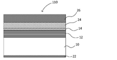
- FIG. 3 is a schematic cross-sectional view showing an example of the reflective mask blank 110 according to the present embodiment.
- the reflective mask blank 110 shown in FIG. 3 has an absorber film 24 for absorbing EUV light on the protective film 14 of the substrate 100 with the multilayer reflective film described above.
- the reflective mask blank 110 may further have another thin film such as a resist film 26 on the absorber film 24.
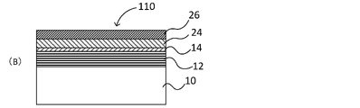
- FIG. 4 is a schematic cross-sectional view showing another example of the reflective mask blank 110.
- the reflective mask blank 110 may have an etching mask film 28 between the absorber film 24 and the resist film 26.
- the absorber film 24 of the reflective mask blank 110 of the present embodiment is formed on the protective film 14.
- the basic function of the absorber film 24 is to absorb EUV light.
- the absorber film 24 may be an absorber film 24 for the purpose of absorbing EUV light, or may be an absorber film 24 having a phase shift function in consideration of the phase difference of EUV light.
- the absorber film 24 having a phase shift function absorbs EUV light and reflects a part of EUV light to shift the phase. That is, in the reflective mask 200 in which the absorber film 24 having a phase shift function is patterned, the portion where the absorber film 24 is formed absorbs EUV light and dims, and the pattern transfer is not adversely affected. Reflects some light.
- the absorber film 24 having a phase shift function is preferably formed so that the phase difference between the reflected light from the absorber film 24 and the reflected light from the multilayer reflective film 12 is 170 degrees to 190 degrees.
- the image contrast of the projected optical image is improved by the light having the inverted phase difference in the vicinity of 180 degrees interfering with each other at the pattern edge portion. As the image contrast is improved, the resolution is increased, and various exposure-related margins such as exposure amount margin and focal margin can be increased.
- the absorber membrane 24 may be a single-layer membrane or a multilayer membrane composed of a plurality of membranes (for example, a lower absorber membrane and an upper absorber membrane).
- a single-layer film the number of steps during mask blank manufacturing can be reduced, so that production efficiency is improved.
- its optical constant and film thickness can be appropriately set so that the upper absorber film becomes an antireflection film at the time of mask pattern defect inspection using light. This improves the inspection sensitivity at the time of mask pattern defect inspection using light.
- a membrane to which oxygen (O), nitrogen (N) or the like for improving oxidation resistance is added to the upper absorber membrane is used, the stability over time is improved.
- the absorber film 24 By making the absorber film 24 a multilayer film in this way, it is possible to add various functions to the absorber film 24.
- the absorber film 24 has a phase shift function, the range of adjustment on the optical surface can be increased by forming the multilayer film, so that it becomes easy to obtain a desired reflectance.
- the material of the absorber film 24 has a function of absorbing EUV light and can be processed by etching or the like (preferably, it can be etched by dry etching of chlorine (Cl) -based gas and / or fluorine (F) -based gas).
- the material is not particularly limited as long as it is a material having a high etching selectivity with respect to the protective film 14. Those having such a function include palladium (Pd), silver (Ag), platinum (Pt), gold (Au), yttrium (Ir), tungsten (W), chromium (Cr), cobalt (Co), and manganese.
- Mn tin
- Sn tantalum
- Ta vanadium
- V nickel
- Hf hafnium
- Fe iron
- Cu tellurium
- Zn magnesium
- Mg germanium
- Al aluminum
- Rh rhodium
- Ru ruthenium
- Mo molybdenum
- Nb niobium
- Ti titanium
- Zr zirconium
- Y yttrium
- At least one metal selected from silicon (Si), or compounds thereof, can be preferably used.
- ruthenium (Ru-based material)
- Ru-based material a material containing ruthenium (Ru) (Ru-based material) as the material of the absorber film 24.
- the composition ratio of Ru and Cr is preferably 15: 1 to 1:20.
- the composition ratio of Ru and Ni is preferably 20: 1 to 1: 4.
- the composition ratio of Ru and Co is preferably 20: 1 to 1: 5.
- the composition ratio of Ru and Al is preferably 20: 1 to 4: 5.
- the composition ratio of Ru and Si is preferably 20: 1 to 1: 1.
- the composition ratio of Ru and Ti is preferably 20: 1 to 1:20.
- the composition ratio of Ru and V is preferably 20: 1 to 1:20.
- the composition ratio of Ru and Ge is preferably 20: 1 to 1: 1.
- the composition ratio of Ru and Nb is preferably 20: 1 to 5: 1.
- the composition ratio of Ru and Mo is preferably 20: 1 to 4: 1.
- the composition ratio of Ru and Sn is preferably 20: 1 to 3: 2.
- the composition ratio of Ru and Te is preferably 20: 1 to 3: 1.
- the composition ratio of Ru and Hf is preferably 20: 1 to 1: 2.
- the composition ratio of Ru and W is preferably 20: 1 to 1:20.
- the composition ratio of Ru and Re is preferably 20: 1 to 1:20.
- the binary Ru-based material has been mainly described, but the ternary Ru-based material (for example, RuCrNi, RuCrCo, RuNiCo, and RuCrW) or the quaternary Ru-based material (for example, RuCrW).
- RuCrNiCo and RuCrCoW can also be used.
- the absorber film 24 may contain elements other than the above-mentioned metals.
- the absorber membrane 24 may contain at least one element selected from the group consisting of nitrogen (N), oxygen (O), carbon (C), and boron (B).
- the material of such an absorber film 24 include RuN, RuCrN, RuCrO and the like.
- Such an absorber film 24 can be etched with a mixed gas of a chlorine-based gas and an oxygen gas.
- the absorber film 24 containing the above-mentioned Ru-based material can be formed by a known method such as a magnetron sputtering method such as a DC sputtering method and an RF sputtering method.
- the absorber film 24 is at least one selected from the group consisting of Ru and Cr, Ni, Co, Al, Si, Ti, V, Ge, Nb, Mo, Sn, Te, Hf, W and Re.
- a film can be formed by a sputtering method using an alloy target containing the above elements.
- the absorber film 24 includes a Ru target and at least one target among Cr, Ni, Co, Al, Si, Ti, V, Ge, Nb, Mo, Sn, Te, Hf, W and Re.
- the film can be formed by the sputtering method (co-sputter method) used.
- the Ru-based material containing Ru and at least one element among Cr, Ni, Co, V, Nb, Mo, W and Re can be dry-etched by a chlorine-based gas containing oxygen or an oxygen gas.
- Ru-based materials containing Ru and at least one of Al, Si, Ti, Ge, Sn and Hf can be dry-etched with an oxygen-free chlorine-based gas.
- chlorine-based gas Cl 2 , SiCl 4 , CHCl 3 , CCl 4 , BCl 3 , and the like can be used. These etching gases may contain an inert gas such as He and / or Ar, if desired.
- the Ru-based material containing Ru and at least one element among Al, Si, Ti, Nb, Mo, Sn, Te, Hf, W and Re can be dry-etched with a fluorine-based gas.
- a fluorine-based gas As the fluorogas, CF 4 , CHF 3 , C 2 F 6 , C 3 F 6 , C 4 F 6 , C 4 F 8 , CH 2 F 2 , C 3 F 8 , SF 6 and the like can be used.
- These etching gases may be used alone or in combination of two or more. These etching gases may contain an inert gas such as He and / or Ar, or an O 2 gas, if necessary.
- the protective film 14 contains a first metal and a second metal. Since the protective film 14 has sufficient resistance to the etching gas used for etching the absorber film 24 described above, it can function as an etching stopper when etching the absorber film 24.
- the protective film 14 contains a first metal and a second metal. Since the protective film 14 has sufficient resistance to the fluorine-based etching gas (for example, XeF 2 + H 2 O) used in the absorber pattern repair step, the fluorine-based etching gas used in the repair step. This can prevent the multilayer reflective film 12 from being damaged.
- the fluorine-based etching gas for example, XeF 2 + H 2 O
- the multilayer reflective film 12 is damaged by the fluorine-based etching gas used in the repair step. While preventing this, the reflectance of the multilayer reflective film 12 can be maintained at a predetermined value or more (for example, 65% or more).
- FIG. 5 is a schematic cross-sectional view showing another example of the reflective mask blank 110.
- the absorber film 24 may include a buffer layer 24b on the side in contact with the protective film 14. That is, the absorber film 24 may include a buffer layer 24b on the side in contact with the protective film 14 and an absorption layer 24c formed on the buffer layer 24b.
- the absorption layer 24c is preferably formed of the same material as the above-mentioned absorber film 24, and more preferably formed of a material containing Ru (Ru-based material).
- the etching selection ratio of the absorption layer 24c to the protective film 14 is not sufficiently high. Even in this case, by interposing the buffer layer 24b between the protective film 14 and the absorbing layer 24c, it is possible to avoid the problem that the etching selectivity of the absorbing layer 24c with respect to the protective film 14 is not high. ..
- the material of the buffer layer 24b is preferably a material containing tantalum (Ta) and one or more elements selected from oxygen (O), nitrogen (N) and boron (B). Examples of such materials include TaO, TaBO, TaN, TaBN and the like.
- the buffer layer 24b containing such a material can be etched with a fluorine-based gas or a chlorine-based gas containing no oxygen.
- the material of the buffer layer 24b is preferably a material containing silicon (Si), and is a material containing silicon (Si) and one or more elements selected from oxygen (O) and nitrogen (N). It is more preferable to have. Examples of such materials include SiO 2 , SiO, SiN, SiON, SiC, SiCO, SiCN, SiCON, MoSi, MoSiO, MoSiN, MoSiON, and the like.
- the buffer layer 24b containing such a material can be etched with a fluorine-based gas.
- the film thickness of the buffer layer 24b is preferably 0.5 nm or more, more preferably 1 nm or more, from the viewpoint of suppressing damage to the protective film 14 and changing the optical characteristics during etching of the absorption layer 24c. Yes, more preferably 2 nm or more.
- the film thickness of the buffer layer 24b is preferably 25 nm or less, more preferably 15 nm or less, still more preferably 10 nm or less, from the viewpoint of reducing the total film thickness of the absorption layer 24c and the buffer layer 24b. Particularly preferably less than 4 nm.
- the protective film 14 contains a first metal and a second metal. Since the protective film 14 has sufficient resistance to the etching gas used for etching the buffer layer 24b described above, it can function as an etching stopper when etching the buffer layer 24b.
- a back surface conductive film 22 for an electrostatic chuck is formed on the second main surface of the substrate 100 (the main surface opposite to the side on which the multilayer reflective film 12 is formed).
- the sheet resistance required for the back surface conductive film 22 for an electrostatic chuck is usually 100 ⁇ / ⁇ ( ⁇ / square) or less.
- the back surface conductive film 22 can be formed by, for example, a magnetron sputtering method or an ion beam sputtering method using a metal such as chromium or tantalum, or a target of an alloy thereof.
- the material of the back surface conductive film 22 is preferably a material containing chromium (Cr) or tantalum (Ta).
- the material of the back surface conductive film 22 is preferably a Cr compound containing at least one selected from boron, nitrogen, oxygen, and carbon in Cr.
- the Cr compound include CrN, CrON, CrCN, CrCON, CrBN, CrBON, CrBCN and CrBOCN.
- the material of the back surface conductive film 22 is preferably Ta (tantalum), an alloy containing Ta, or a Ta compound containing at least one of boron, nitrogen, oxygen, and carbon in any of these.
- Ta compound examples include TaB, TaN, TaO, TaON, TaCON, TaBN, TaBO, TaBON, TaBCON, TaHf, TaHO, TaHN, TaHON, TaHON, TaHCON, TaSi, TaSiO, TaSiT, TaSiN, TaSiN, , TaSiON, TaSiCON and the like.
- the film thickness of the back surface conductive film 22 is not particularly limited as long as it functions as a film for an electrostatic chuck, but is usually 10 nm to 200 nm. Further, the back surface conductive film 22 preferably has a function of adjusting the stress on the second main surface side of the reflective mask blank 110. That is, the back surface conductive film 22 is adjusted so that the reflective mask blank 110 becomes flat by balancing the stress generated by the formation of the thin film on the first main surface and the stress on the second main surface. It is preferable to have a function to perform.
- An etching mask film 28 may be formed on the absorber film 24.
- the material of the etching mask film 28 it is preferable to use a material having a high etching selectivity of the absorber film 24 with respect to the etching mask film 28.
- the etching selectivity of the absorber film 24 with respect to the etching mask film 28 is preferably 1.5 or more, and more preferably 3 or more.
- tantalum (Ta), oxygen (O), and nitrogen (N) are used as materials for the etching mask film 28.
- a material containing one or more elements selected from boron (B) can be used. Examples of such materials include TaO, TaBO, TaN, TaBN and the like.
- a material containing silicon (Si) may be used as the material of the etching mask film 28.
- Silicon (Si) and one or more elements selected from oxygen (O) and nitrogen (N) are preferably used. Examples of such materials include SiO 2 , SiO, SiN, SiON, SiC, SiCO, SiCN, SiCON, MoSi, MoSiO, MoSiN, MoSiON, and the like.
- chromium or a chromium compound can be used as the material of the etching mask film 28.
- chromium compounds include materials containing Cr and at least one element selected from N, O, C and H.
- the etching mask film 28 more preferably contains CrN, CrO, CrC, CrON, CrOC, CrCN or CrOCN, and is a CrO-based film (CrO film, CrON film, CrOC film or CrOCN film) containing chromium and oxygen. Is more preferable.
- the film thickness of the etching mask film 28 is preferably 3 nm or more in order to form the pattern on the absorber film 24 with high accuracy.
- the film thickness of the etching mask film 28 is preferably 15 nm or less in order to reduce the film thickness of the resist film 26.
- the reflective mask 200 according to the present embodiment can be manufactured by using the reflective mask blank 110 according to the present embodiment.
- an example of a method for manufacturing a reflective mask will be described.
- FIG. 6A to 6E are schematic views showing an example of a method for manufacturing the reflective mask 200.
- the substrate 10, the multilayer reflective film 12 formed on the substrate 10, the protective film 14 formed on the multilayer reflective film 12, and the protective film 14 were formed.
- a reflective mask blank 110 having an absorber film 24 is prepared (FIG. 6A).
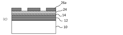
- a resist film 26 is formed on the absorber film 24 (FIG. 6B).
- a pattern is drawn on the resist film 26 by an electron beam drawing apparatus, and a resist pattern 26a is formed by further undergoing a development / rinsing step (FIG. 6C).
- etching gas of the absorber film 24 for example, a fluorine-based gas and / or a chlorine-based gas can be used.
- Fluorine-based gases include CF 4 , CHF 3 , C2F 6 , C 3 F 6 , C 4 F 6 , C 4 F 8 , CH 2 F 2 , CH 3 F, C 3 F 8 , SF 6 and F 2 .
- Etc. can be used.
- Cl 2 , SiCl 4 , CHCl 3 , CCl 4 , BCl 3 , and the like can be used.
- a mixed gas containing a fluorine-based gas and / or a chlorine-based gas and O 2 in a predetermined ratio can be used.
- These etching gases may further contain an inert gas such as He and / or Ar, if desired.
- the resist pattern 26a is removed with a resist stripping solution.
- the reflective mask 200 of the present embodiment is obtained by undergoing a wet cleaning step using an acidic or alkaline aqueous solution (FIG. 6E).
- a pattern is formed on the etching mask film 28 by using the resist pattern 26a as a mask. After that, a step of forming a pattern on the absorber film 24 using the etching mask pattern as a mask is added.
- the reflective mask 200 thus obtained has a structure in which a multilayer reflective film 12, a protective film 14, and an absorber pattern 24a are laminated on a substrate 10.
- the region 30 where the multilayer reflective film 12 (including the protective film 14) is exposed has a function of reflecting EUV light.
- the region 32 in which the multilayer reflective film 12 (including the protective film 14) is covered with the absorber pattern 24a has a function of absorbing EUV light.
- the thickness of the absorber pattern 24a having a reflectance of, for example, 2.5% or less can be made thinner than before, so that a finer pattern can be transferred. Can be transferred to.
- a transfer pattern can be formed on a semiconductor substrate by lithography using the reflective mask 200 of the present embodiment. This transfer pattern has a shape in which the pattern of the reflective mask 200 is transferred.
- a semiconductor device can be manufactured by forming a transfer pattern on a semiconductor substrate with a reflective mask 200.
- FIG. 7 shows the pattern transfer device 50.
- the pattern transfer device 50 includes a laser plasma X-ray source 52, a reflective mask 200, a reduction optical system 54, and the like.
- An X-ray reflection mirror is used as the reduction optical system 54.
- the pattern reflected by the reflective mask 200 is usually reduced to about 1/4 by the reduction optical system 54.
- a wavelength band of 13 to 14 nm is used as the exposure wavelength, and the optical path is preset so as to be in a vacuum.
- the EUV light generated by the laser plasma X-ray source 52 is incident on the reflective mask 200.
- the light reflected by the reflective mask 200 is transferred onto the resisted semiconductor substrate 56 via the reduction optical system 54.
- the light reflected by the reflective mask 200 is incident on the reduced optical system 54.
- the light incident on the reduction optical system 54 forms a transfer pattern on the resist layer on the resist-attached semiconductor substrate 56.
- a resist pattern can be formed on the resist-attached semiconductor substrate 56.
- etching the semiconductor substrate 56 using the resist pattern as a mask for example, a predetermined wiring pattern can be formed on the semiconductor substrate.
- a semiconductor device is manufactured by going through such a process and other necessary steps.
- a 6025 size (about 152 mm ⁇ 152 mm ⁇ 6.35 mm) substrate 10 on which the first main surface and the second main surface were polished was prepared.
- the substrate 10 is a substrate made of low thermal expansion glass (SiO 2 -TiO 2 glass).
- the main surface of the substrate 10 was polished by a rough polishing process, a precision polishing process, a local processing process, and a touch polishing process.
- the multilayer reflective film 12 was formed on the main surface (first main surface) of the substrate 10.
- the multilayer reflective film 12 formed on the substrate 10 is a periodic multilayer reflective film 12 composed of Mo and Si in order to obtain a multilayer reflective film 12 suitable for EUV light having a wavelength of 13.5 nm.
- the multilayer reflective film 12 was formed by alternately laminating Mo film and Si film on the substrate 10 by an ion beam sputtering method using a Mo target and a Si target and using krypton (Kr) as a process gas.
- a Si film was formed with a thickness of 4.2 nm
- a Mo film was formed with a thickness of 2.8 nm. This was set as one cycle, and 40 cycles were laminated in the same manner to form the multilayer reflective film 12.
- the Si material layer 16 was formed on the multilayer reflective film 12.
- the multilayer reflective film 12 and the Si material layer 16 were continuously formed by an ion beam sputtering method.
- the Si material layer 16 was formed into a film having a thickness of 4.0 nm using a Si target and krypton (Kr) as a process gas.
- a protective layer 18 was formed on the Si material layer 16.
- the protective layer 18 was formed by a magnetron sputtering method (co-sputtering method) in an Ar gas atmosphere using two metal targets of the protective layer material shown in Table 3.
- the composition of the protective layer 18 was measured by X-ray photoelectron spectroscopy (XPS). Table 3 below shows the composition and film thickness of the protective layer 18 in Examples and Comparative Examples.
- Electron beam acceleration voltage 1kV XeF 2 temperature: 0 ° C H 2 O temperature: -42 ° C
- Electron beam irradiation time per unit pixel 1.5 nm x 1.5 nm): 4.00e- 8 [s]
- Definition of 1 loop The electron beam is repeatedly scanned in the left-right direction at a predetermined interval in the vertical direction, and the entire area of 500 nm ⁇ 500 nm is scanned in one loop.
- Reflective mask blank 110 Apart from the substrate 100 with a multilayer reflective film used in the repair resistance test described above, the substrates 100 with a multilayer reflective film of Examples 1 to 3 and Comparative Example 1 were produced. Using the prepared substrate 100 with a multilayer reflective film, a reflective mask blank 110 including an absorber film 24 was manufactured. Hereinafter, a method for manufacturing the reflective mask blank 110 will be described.
- An absorber film 24 (phase shift film) made of a RuCr film was formed on the protective layer 18 of the substrate 100 with a multilayer reflective film by the DC magnetron sputtering method.
- the RuCr film was formed using a RuCr target so as to have a film thickness of 45.0 nm in an Ar gas atmosphere.
- a back surface conductive film 22 made of CrN was formed on the second main surface (back side main surface) of the substrate 10 by a magnetron sputtering method (reactive sputtering method) under the following conditions.
- Conditions for forming the back surface conductive film 22 Cr target, mixed gas atmosphere of Ar and N 2 (Ar: 90 atomic%, N: 10 atomic%), film thickness 20 nm.
- the reflective mask blanks 110 of Examples 1 to 3 and Comparative Example 1 were manufactured.
- Reflective mask 200 Next, the reflective mask 200 was manufactured using the reflective mask blank 110 described above. The production of the reflective mask 200 will be described with reference to FIGS. 6B to 6E.
- a resist film 26 was formed on the absorber film 24 of the reflective mask blank 110.
- a desired pattern such as a circuit pattern was drawn (exposed) on the resist film 26, and further developed and rinsed to form a predetermined resist pattern 26a (FIG. 6C).
- a pattern 24a was formed (FIG. 6D).
- the number of loops of the protective film 14 of the substrate 100 with the multilayer reflective film of Examples 1 to 3 was larger than the number of loops of the protective film of the substrate with the multilayer reflective film of Comparative Example 1. That is, the protective layer 18 (protective film 14) of the substrate 100 with the multilayer reflective film of Examples 1 to 3 has high resistance to repair by electron beam irradiation using a fluorine-based etching gas (XeF 2 + H 2 O). Do you get it.
- a fluorine-based etching gas XeF 2 + H 2 O
- the reflectance of the protective layer 18 (protective film 14) of the reflective masks 200 of Examples 1 to 3 was 65% or more, and maintained a predetermined value or more.
Landscapes
- Physics & Mathematics (AREA)
- General Physics & Mathematics (AREA)
- Engineering & Computer Science (AREA)
- Condensed Matter Physics & Semiconductors (AREA)
- Manufacturing & Machinery (AREA)
- Computer Hardware Design (AREA)
- Microelectronics & Electronic Packaging (AREA)
- Power Engineering (AREA)
- Preparing Plates And Mask In Photomechanical Process (AREA)
- Exposure And Positioning Against Photoresist Photosensitive Materials (AREA)
- Exposure Of Semiconductors, Excluding Electron Or Ion Beam Exposure (AREA)
Abstract
Description
基板と、該基板の上に設けられた多層反射膜と、該多層反射膜の上に設けられた保護膜とを有する多層反射膜付き基板であって、
前記保護膜は、第1の金属と第2の金属とを含み、
前記第1の金属のフッ化物の標準生成自由エネルギーは、RuF5の標準生成自由エネルギーよりも高く、
前記第2の金属は、波長13.5nmにおける消衰係数が0.03以下であることを特徴とする多層反射膜付き基板。
前記第1の金属は、イリジウム(Ir)であることを特徴とする構成1記載の多層反射膜付き基板。
前記第1の金属は、ロジウム(Rh)であることを特徴とする構成1記載の多層反射膜付き基板。
前記第2の金属は、ジルコニウム(Zr)及びルテニウム(Ru)から選択される少なくとも1つであることを特徴とする構成1から3のうちいずれかに記載の多層反射膜付き基板。
構成1から4のうちいずれかに記載の多層反射膜付き基板の前記保護膜の上に、吸収体膜を備えることを特徴とする反射型マスクブランク。
前記吸収体膜は、ルテニウム(Ru)を含むことを特徴とする構成5に記載の反射型マスクブランク。
前記吸収体膜は、バッファ層と、該バッファ層の上に設けられた吸収層とを有し、
前記バッファ層は、タンタル(Ta)又はケイ素(Si)を含み、
前記吸収層は、ルテニウム(Ru)を含むことを特徴とする構成5又は6に記載の反射型マスクブランク。
構成5から7のうちいずれかに記載の反射型マスクブランクの前記吸収体膜をパターニングした吸収体パターンを備えることを特徴とする反射型マスク。
構成8に記載の反射型マスクを用いて、露光装置を使用したリソグラフィプロセスを行い、被転写体に転写パターンを形成する工程を有することを特徴とする半導体装置の製造方法。
基板10は、EUV光による露光時の熱による転写パターンの歪みを防止するため、0±5ppb/℃の範囲内の低熱膨張係数を有するものが好ましく用いられる。この範囲の低熱膨張係数を有する素材としては、例えば、SiO2-TiO2系ガラス、多成分系ガラスセラミックス等を用いることができる。
多層反射膜12は、屈折率の異なる元素を主成分とする複数の層が周期的に積層された構成を有している。一般的に、多層反射膜12は、高屈折率材料である軽元素又はその化合物の薄膜(高屈折率層)と、低屈折率材料である重元素又はその化合物の薄膜(低屈折率層)とが交互に40~60周期程度積層された多層膜からなる。多層反射膜12を形成するために、基板10側から高屈折率層と低屈折率層をこの順に複数周期積層してもよい。この場合、1つの(高屈折率層/低屈折率層)の積層構造が、1周期となる。
後述する反射型マスク200の製造工程におけるドライエッチング及び洗浄から多層反射膜12を保護するために、多層反射膜12の上に、又は多層反射膜12の表面に接するように保護膜14を形成することができる。また、保護膜14は、電子線(EB)を用いた転写パターン(吸収体パターン)の黒欠陥修正の際に、多層反射膜12を保護する機能も有している。多層反射膜12の上に保護膜14が形成されることにより、反射型マスク200を製造する際の多層反射膜12の表面へのダメージを抑制することができる。その結果、多層反射膜12のEUV光に対する反射率特性が良好となる。


保護膜14に窒素(N)が含まれる場合、N含有量は、0.1原子%以上が好ましく、1原子%以上がより好ましい。また、N含有量は、50原子%以下が好ましく、25原子%以下であることがより好ましい。
保護膜14の材料が、Ir、Zr及びNを含む場合、N含有量は0.1~50原子%が好ましく、1~25原子%がより好ましい。
保護膜14の材料が、Ir、Ru及びNを含む場合、N含有量は0.1~15原子%が好ましく、1~10原子%がより好ましい。
保護膜14の材料が、Rh、Zr及びNを含む場合、N含有量は0.1~50原子%が好ましく、1~25原子%がより好ましい。
保護膜14の材料が、Rh、Ru及びNを含む場合、N含有量は0.1~15原子%が好ましく、1~10原子%がより好ましい。
保護膜14の材料が、Ir及びZrを含む場合、IrとZrの組成比(Ir:Zr)は、9:1~1:9であることが好ましく、4:1~1:4であることがより好ましい。
保護膜14の材料が、Ir及びRuを含む場合、IrとRuの組成比(Ir:Ru)は、9:1~1:9であることが好ましく、4:1~1:4であることがより好ましい。
保護膜14の材料が、Ir及びYを含む場合、IrとYの組成比(Ir:Y)は、9:1~1:9であることが好ましく、7:3~1:4であることがより好ましい。
保護膜14の材料が、Ir及びLaを含む場合、IrとLaの組成比(Ir:La)は、9:1~1:1であることが好ましく、17:3~3:2であることがより好ましい。
保護膜14の材料が、Ir及びNbを含む場合、IrとNbの組成比(Ir:Nb)は、9:1~1:1であることが好ましく、17:3~3:2であることがより好ましい。
保護膜14の材料が、Ir及びRbを含む場合、IrとRbの組成比(Ir:Rb)は、9:1~1:1であることが好ましく、17:3~3:2であることがより好ましい。
保護膜14の材料が、Ir及びTiを含む場合、IrとTiの組成比(Ir:Ti)は、9:1~1:1であることが好ましく、17:3~3:2であることがより好ましい。
保護膜14の材料が、Pd及びZrを含む場合、PdとZrの組成比(Pd:Zr)は、9:1~1:9であることが好ましく、4:1~1:4であることがより好ましい。
保護膜14の材料が、Pd及びRuを含む場合、PdとRuの組成比(Pd:Ru)は、9:1~1:9であることが好ましく、4:1~1:4であることがより好ましい。
保護膜14の材料が、Pd及びYを含む場合、PdとYの組成比(Pd:Y)は、9:1~1:9であることが好ましく、7:3~1:4であることがより好ましい。
保護膜14の材料が、Pd及びLaを含む場合、PdとLaの組成比(Pd:La)は、9:1~1:1であることが好ましく、17:3~3:2であることがより好ましい。
保護膜14の材料が、Pd及びNbを含む場合、PdとNbの組成比(Pd:Nb)は、9:1~1:1であることが好ましく、17:3~3:2であることがより好ましい。 保護膜14の材料が、Pd及びRbを含む場合、PdとRbの組成比(Pd:Rb)は、9:1~1:1であることが好ましく、17:3~3:2であることがより好ましい。
保護膜14の材料が、Pd及びTiを含む場合、PdとTiの組成比(Pd:Ti)は、9:1~1:1であることが好ましく、17:3~3:2であることがより好ましい。 保護膜14の材料が、Au及びZrを含む場合、AuとZrの組成比(Au:Zr)は、9:1~1:9であることが好ましく、4:1~1:4であることがより好ましい。
保護膜14の材料が、Au及びRuを含む場合、AuとRuの組成比(Au:Ru)は、9:1~1:9であることが好ましく、4:1~1:4であることがより好ましい。
保護膜14の材料が、Au及びYを含む場合、AuとYの組成比(Au:Y)は、9:1~1:9であることが好ましく、7:3~1:4であることがより好ましい。
保護膜14の材料が、Au及びLaを含む場合、AuとLaの組成比(Au:La)は、9:1~1:1であることが好ましく、17:3~3:2であることがより好ましい。
保護膜14の材料が、Au及びNbを含む場合、AuとNbの組成比(Au:Nb)は、9:1~1:1であることが好ましく、17:3~3:2であることがより好ましい。
保護膜14の材料が、Au及びRbを含む場合、AuとRbの組成比(Au:Rb)は9:1~1:1であることが好ましく、17:3~3:2であることがより好ましい。
保護膜14の材料が、Au及びTiを含む場合、AuとTiの組成比(Au:Ti)は、9:1~1:1であることが好ましく、17:3~3:2であることがより好ましい。
保護膜14の材料が、Pt及びZrを含む場合、PtとZrの組成比(Pt:Zr)は、9:1~1:9であることが好ましく、4:1~1:4であることがより好ましい。
保護膜14の材料が、Pt及びRuを含む場合、PtとRuの組成比(Pt:Ru)は、9:1~1:9であることが好ましく、4:1~1:4であることがより好ましい。
保護膜14の材料が、Pt及びYを含む場合、PtとYの組成比(Pt:Y)は、9:1~1:9であることが好ましく、7:3~1:4であることがより好ましい。
保護膜14の材料が、Pt及びLaを含む場合、PtとLaの組成比(Pt:La)は、9:1~1:1であることが好ましく、17:3~3:2であることがより好ましい。
保護膜14の材料が、Pt及びNbを含む場合、PtとNbの組成比(Pt:Nb)は、9:1~1:1であることが好ましく、17:3~3:2であることがより好ましい。
保護膜14の材料が、Pt及びRbを含む場合、PtとRbの組成比(Pt:Rb)は、9:1~1:1であることが好ましく、17:3~3:2であることがより好ましい。
保護膜14の材料が、Pt及びTiを含む場合、PtとTiの組成比(Pt:Ti)は、9:1~1:1であることが好ましく、17:3~3:2であることがより好ましい。
保護膜14の材料が、Rh及びZrを含む場合、RhとZrの組成比(Rh:Zr)は、9:1~1:9であることが好ましく、4:1~1:4であることがより好ましい。
保護膜14の材料が、Rh及びRuを含む場合、RhとRuの組成比(Rh:Ru)は、9:1~1:9であることが好ましく、4:1~1:4であることがより好ましい。
保護膜14の材料が、Rh及びYを含む場合、RhとYの組成比(Rh:Y)は、9:1~1:9であることが好ましく、7:3~1:4であることがより好ましい。
保護膜14の材料が、Rh及びLaを含む場合、RhとLaの組成比(Rh:La)は、9:1~1:1であることが好ましく、17:3~3:2であることがより好ましい。
保護膜14の材料が、Rh及びNbを含む場合、RhとNbの組成比(Rh:Nb)は、9:1~1:1であることが好ましく、17:3~3:2であることがより好ましい。
保護膜14の材料が、Rh及びRbを含む場合、RhとRbの組成比(Rh:Rb)は、9:1~1:1であることが好ましく、17:3~3:2であることがより好ましい。
保護膜14の材料が、Rh及びTiを含む場合、RhとTiの組成比(Rh:Ti)は、9:1~1:1であることが好ましく、17:3~3:2であることがより好ましい。
本実施形態の反射型マスクブランク110の吸収体膜24は、保護膜14の上に形成される。吸収体膜24の基本的な機能は、EUV光を吸収することである。吸収体膜24は、EUV光の吸収を目的とした吸収体膜24であってもよいし、EUV光の位相差も考慮した位相シフト機能を有する吸収体膜24であってもよい。位相シフト機能を有する吸収体膜24とは、EUV光を吸収するとともに、EUV光の一部を反射させて位相をシフトさせるものである。すなわち、位相シフト機能を有する吸収体膜24がパターニングされた反射型マスク200において、吸収体膜24が形成されている部分では、EUV光を吸収して減光しつつパターン転写に悪影響がないレベルで一部の光を反射させる。また、吸収体膜24が形成されていない領域(フィールド部)では、EUV光は、保護膜14を介して多層反射膜12で反射される。そのため、位相シフト機能を有する吸収体膜24からの反射光と、フィールド部からの反射光との間に所望の位相差が生ずる。位相シフト機能を有する吸収体膜24は、吸収体膜24からの反射光と、多層反射膜12からの反射光との位相差が170度から190度となるように形成されることが好ましい。180度近傍の反転した位相差の光同士がパターンエッジ部で干渉し合うことにより、投影光学像の像コントラストが向上する。その像コントラストの向上に伴って解像度が上がり、露光量裕度、及び焦点裕度等の露光に関する各種裕度を大きくすることができる。
吸収体膜24の材料が、Ru及びNiを含む場合、RuとNiの組成比(Ru:Ni)は、20:1~1:4であることが好ましい。
吸収体膜24の材料が、Ru及びCoを含む場合、RuとCoの組成比(Ru:Co)は、20:1~1:5であることが好ましい。
吸収体膜24の材料が、Ru及びAlを含む場合、RuとAlの組成比(Ru:Al)は、20:1~4:5であることが好ましい。
吸収体膜24の材料が、Ru及びSiを含む場合、RuとSiの組成比(Ru:Si)は、20:1~1:1であることが好ましい。
吸収体膜24の材料が、Ru及びTiを含む場合、RuとTiの組成比(Ru:Ti)は、20:1~1:20であることが好ましい。
吸収体膜24の材料が、Ru及びVを含む場合、RuとVの組成比(Ru:V)は、20:1~1:20あることが好ましい。
吸収体膜24の材料が、RuとGeを含む場合、RuとGeの組成比(Ru:Ge)は、20:1~1:1であることが好ましい。
吸収体膜24の材料が、Ru及びNbを含む場合、RuとNbの組成比(Ru:Nb)は、20:1~5:1であることが好ましい。
吸収体膜24の材料が、Ru及びMoを含む場合、RuとMoの組成比(Ru:Mo)は、20:1~4:1であることが好ましい。
吸収体膜24の材料が、Ru及びSnを含む場合、RuとSnの組成比(Ru:Sn)は、20:1~3:2であることが好ましい。
吸収体膜24の材料が、Ru及びTeを含む場合、RuとTeの組成比(Ru:Te)は、20:1~3:1であることが好ましい。
吸収体膜24の材料が、Ru及びHfを含む場合、RuとHfの組成比(Ru:Hf)は、20:1~1:2であることが好ましい。
吸収体膜24の材料が、Ru及びWを含む場合、RuとWの組成比(Ru:W)は、20:1~1:20であることが好ましい。
吸収体膜24の材料が、Ru及びReを含む場合、RuとReの組成比(Ru:Re)は、20:1~1:20であることが好ましい。
基板100の第2主表面(多層反射膜12が形成された側と反対側の主表面)の上には、静電チャック用の裏面導電膜22が形成される。静電チャック用として、裏面導電膜22に求められるシート抵抗は、通常100Ω/□(Ω/square)以下である。裏面導電膜22は、例えば、クロム又はタンタル等の金属、又はそれらの合金のターゲットを使用したマグネトロンスパッタリング法又はイオンビームスパッタリング法によって形成することができる。裏面導電膜22の材料は、クロム(Cr)又はタンタル(Ta)を含む材料であることが好ましい。例えば、裏面導電膜22の材料は、Crに、ホウ素、窒素、酸素、及び炭素から選択される少なくとも一つを含有したCr化合物であることが好ましい。Cr化合物としては、例えば、CrN、CrON、CrCN、CrCON、CrBN、CrBON、CrBCN及びCrBOCNなどを挙げることができる。また、裏面導電膜22の材料は、Ta(タンタル)、Taを含有する合金、又はこれらのいずれかにホウ素、窒素、酸素、及び炭素の少なくとも一つを含有したTa化合物であることが好ましい。Ta化合物としては、例えば、TaB、TaN、TaO、TaON、TaCON、TaBN、TaBO、TaBON、TaBCON、TaHf、TaHO、TaHN、TaHON、TaHON、TaHCON、TaSi、TaSiO、TaSiN、TaSiONCON、TaSi、TaSiO、TaSiN、TaSiON、及びTaSiCONなどを挙げることができる。
吸収体膜24の上には、エッチングマスク膜28を形成してもよい。エッチングマスク膜28の材料としては、エッチングマスク膜28に対する吸収体膜24のエッチング選択比が高い材料を用いることが好ましい。エッチングマスク膜28に対する吸収体膜24のエッチング選択比は、1.5以上が好ましく、3以上が更に好ましい。
本実施形態による反射型マスクブランク110を使用して、本実施形態の反射型マスク200を製造することができる。以下、反射型マスクの製造方法の例について説明する。
本実施形態の反射型マスク200を使用したリソグラフィーにより、半導体基板上に転写パターンを形成することができる。この転写パターンは、反射型マスク200のパターンが転写された形状を有している。半導体基板上に反射型マスク200によって転写パターンを形成することによって、半導体装置を製造することができる。
まず、第1主表面及び第2主表面が研磨された6025サイズ(約152mm×152mm×6.35mm)の基板10を準備した。この基板10は、低熱膨張ガラス(SiO2-TiO2系ガラス)からなる基板である。基板10の主表面は、粗研磨加工工程、精密研磨加工工程、局所加工工程、及びタッチ研磨加工工程によって研磨した。
実施例1~3及び比較例1の多層反射膜付き基板100を用いて、保護膜14(保護層18)のリペア耐性及び反射率を評価する試験を行った。
まず、リペア装置を用いて、保護膜14のリペア耐性を評価する試験を行った。具体的には、保護膜14の周囲にフッ素系エッチングガス(XeF2+H2O)を供給しつつ、保護膜14の表面に電子線を照射する処理を繰り返した。試験条件は、以下の通りである。
(リペア耐性試験条件)
電子線の加速電圧:1kV
XeF2温度:0℃
H2O温度:-42℃
単位ピクセル(1.5nm×1.5nm)当たりの電子線照射時間:4.00e-8[s]
1ループの定義:上下方向に所定の間隔を空けて、電子線を左右方向に繰り返し走査し、500nm×500nmの領域全面を走査し終えるまでを1ループとする。
上述のリペア耐性試験に使用した多層反射膜付き基板100とは別に、実施例1~3及び比較例1の多層反射膜付き基板100を作製した。作製した多層反射膜付き基板100を用いて、吸収体膜24を含む反射型マスクブランク110を製造した。以下、反射型マスクブランク110の製造方法について、説明する。
裏面導電膜22の形成条件:Crターゲット、ArとN2の混合ガス雰囲気(Ar:90原子%、N:10原子%)、膜厚20nm。
次に、上述の反射型マスクブランク110を用いて、反射型マスク200を製造した。図6B~6Eを参照して反射型マスク200の製造について説明する。
製造した実施例1~3及び比較例1の反射型マスク200を用いて、保護膜14(保護層18)の反射率を評価する試験を行った。

12 多層反射膜
14 保護膜
16 Si材料層
18 保護層
22 裏面導電膜
24 吸収体膜
24a 吸収体パターン
24b バッファ層
24c 吸収層
26 レジスト膜
28 エッチングマスク膜
100 多層反射膜付き基板
110 反射型マスクブランク
200 反射型マスク
Claims (9)
- 基板と、該基板の上に設けられた多層反射膜と、該多層反射膜の上に設けられた保護膜とを有する多層反射膜付き基板であって、
前記保護膜は、第1の金属と第2の金属とを含み、
前記第1の金属のフッ化物の標準生成自由エネルギーは、RuF5の標準生成自由エネルギーよりも高く、
前記第2の金属は、波長13.5nmにおける消衰係数が0.03以下であることを特徴とする多層反射膜付き基板。 - 前記第1の金属は、イリジウム(Ir)であることを特徴とする請求項1記載の多層反射膜付き基板。
- 前記第1の金属は、ロジウム(Rh)であることを特徴とする請求項1記載の多層反射膜付き基板。
- 前記第2の金属は、ジルコニウム(Zr)及びルテニウム(Ru)から選択される少なくとも1つであることを特徴とする請求項1から3のうちのいずれか1項に記載の多層反射膜付き基板。
- 請求項1から4のうちいずれか1項に記載の多層反射膜付き基板の前記保護膜の上に、吸収体膜を備えることを特徴とする反射型マスクブランク。
- 前記吸収体膜は、ルテニウム(Ru)を含むことを特徴とする請求項5に記載の反射型マスクブランク。
- 前記吸収体膜は、バッファ層と、該バッファ層の上に設けられた吸収層とを有し、
前記バッファ層は、タンタル(Ta)又はケイ素(Si)を含み、
前記吸収層は、ルテニウム(Ru)を含むことを特徴とする請求項5又は6に記載の反射型マスクブランク。 - 請求項5から7のうちいずれか1項に記載の反射型マスクブランクの前記吸収体膜をパターニングした吸収体パターンを備えることを特徴とする反射型マスク。
- 請求項8に記載の反射型マスクを用いて、露光装置を使用したリソグラフィプロセスを行い、被転写体に転写パターンを形成する工程を有することを特徴とする半導体装置の製造方法。
Priority Applications (3)
| Application Number | Priority Date | Filing Date | Title |
|---|---|---|---|
| US18/039,192 US20230418148A1 (en) | 2020-12-25 | 2021-12-16 | Multilayer reflective film-equipped substrate, reflective mask blank, reflective mask, and method for producing semiconductor device |
| JP2022572256A JPWO2022138434A1 (ja) | 2020-12-25 | 2021-12-16 | |
| KR1020237015136A KR20230119111A (ko) | 2020-12-25 | 2021-12-16 | 다층 반사막 구비 기판, 반사형 마스크 블랭크, 반사형 마스크 및 반도체 장치의 제조 방법 |
Applications Claiming Priority (2)
| Application Number | Priority Date | Filing Date | Title |
|---|---|---|---|
| JP2020-217665 | 2020-12-25 | ||
| JP2020217665 | 2020-12-25 |
Publications (1)
| Publication Number | Publication Date |
|---|---|
| WO2022138434A1 true WO2022138434A1 (ja) | 2022-06-30 |
Family
ID=82159285
Family Applications (1)
| Application Number | Title | Priority Date | Filing Date |
|---|---|---|---|
| PCT/JP2021/046485 WO2022138434A1 (ja) | 2020-12-25 | 2021-12-16 | 多層反射膜付き基板、反射型マスクブランク、反射型マスク、及び半導体装置の製造方法 |
Country Status (5)
| Country | Link |
|---|---|
| US (1) | US20230418148A1 (ja) |
| JP (1) | JPWO2022138434A1 (ja) |
| KR (1) | KR20230119111A (ja) |
| TW (1) | TW202240277A (ja) |
| WO (1) | WO2022138434A1 (ja) |
Cited By (2)
| Publication number | Priority date | Publication date | Assignee | Title |
|---|---|---|---|---|
| US20240160096A1 (en) * | 2022-07-05 | 2024-05-16 | AGC Inc. | Reflective mask blank, reflective mask, method of manufacturing reflective mask blank, and method of manufacturing reflective mask |
| JP7557098B1 (ja) | 2024-04-11 | 2024-09-26 | 株式会社トッパンフォトマスク | 反射型フォトマスクブランク、反射型フォトマスク及び反射型フォトマスクの製造方法 |
Citations (6)
| Publication number | Priority date | Publication date | Assignee | Title |
|---|---|---|---|---|
| JP2003318104A (ja) * | 2002-04-18 | 2003-11-07 | Samsung Electronics Co Ltd | キャッピング層を有する反射フォトマスクおよびその製造方法 |
| JP2006173497A (ja) * | 2004-12-17 | 2006-06-29 | Nikon Corp | 光学素子及びこれを用いた投影露光装置 |
| JP2010518594A (ja) * | 2007-02-05 | 2010-05-27 | カール・ツァイス・エスエムティー・アーゲー | 第1および第2付加中間層を備えるeuvリソグラフィ装置用多層反射光学素子 |
| JP2011029334A (ja) * | 2009-07-23 | 2011-02-10 | Toshiba Corp | 反射型露光用マスクおよび半導体装置の製造方法 |
| US20150010854A1 (en) * | 2013-07-02 | 2015-01-08 | Samsung Electronics Co., Ltd. | Reflective Photomask Blanks and Reflective Photomasks |
| WO2015012151A1 (ja) * | 2013-07-22 | 2015-01-29 | Hoya株式会社 | 多層反射膜付き基板、euvリソグラフィー用反射型マスクブランク、euvリソグラフィー用反射型マスク及びその製造方法、並びに半導体装置の製造方法 |
Family Cites Families (3)
| Publication number | Priority date | Publication date | Assignee | Title |
|---|---|---|---|---|
| JP5371162B2 (ja) | 2000-10-13 | 2013-12-18 | 三星電子株式会社 | 反射型フォトマスク |
| JP6377361B2 (ja) | 2013-02-11 | 2018-08-22 | Hoya株式会社 | 多層反射膜付き基板及びその製造方法、反射型マスクブランクの製造方法、反射型マスクの製造方法、並びに半導体装置の製造方法 |
| KR102239726B1 (ko) | 2013-09-11 | 2021-04-12 | 호야 가부시키가이샤 | 다층 반사막을 구비한 기판, euv 리소그래피용 반사형 마스크 블랭크, euv 리소그래피용 반사형 마스크 및 그 제조 방법과 반도체 장치의 제조 방법 |
-
2021
- 2021-12-16 JP JP2022572256A patent/JPWO2022138434A1/ja active Pending
- 2021-12-16 WO PCT/JP2021/046485 patent/WO2022138434A1/ja active Application Filing
- 2021-12-16 KR KR1020237015136A patent/KR20230119111A/ko unknown
- 2021-12-16 US US18/039,192 patent/US20230418148A1/en active Pending
- 2021-12-23 TW TW110148346A patent/TW202240277A/zh unknown
Patent Citations (6)
| Publication number | Priority date | Publication date | Assignee | Title |
|---|---|---|---|---|
| JP2003318104A (ja) * | 2002-04-18 | 2003-11-07 | Samsung Electronics Co Ltd | キャッピング層を有する反射フォトマスクおよびその製造方法 |
| JP2006173497A (ja) * | 2004-12-17 | 2006-06-29 | Nikon Corp | 光学素子及びこれを用いた投影露光装置 |
| JP2010518594A (ja) * | 2007-02-05 | 2010-05-27 | カール・ツァイス・エスエムティー・アーゲー | 第1および第2付加中間層を備えるeuvリソグラフィ装置用多層反射光学素子 |
| JP2011029334A (ja) * | 2009-07-23 | 2011-02-10 | Toshiba Corp | 反射型露光用マスクおよび半導体装置の製造方法 |
| US20150010854A1 (en) * | 2013-07-02 | 2015-01-08 | Samsung Electronics Co., Ltd. | Reflective Photomask Blanks and Reflective Photomasks |
| WO2015012151A1 (ja) * | 2013-07-22 | 2015-01-29 | Hoya株式会社 | 多層反射膜付き基板、euvリソグラフィー用反射型マスクブランク、euvリソグラフィー用反射型マスク及びその製造方法、並びに半導体装置の製造方法 |
Cited By (2)
| Publication number | Priority date | Publication date | Assignee | Title |
|---|---|---|---|---|
| US20240160096A1 (en) * | 2022-07-05 | 2024-05-16 | AGC Inc. | Reflective mask blank, reflective mask, method of manufacturing reflective mask blank, and method of manufacturing reflective mask |
| JP7557098B1 (ja) | 2024-04-11 | 2024-09-26 | 株式会社トッパンフォトマスク | 反射型フォトマスクブランク、反射型フォトマスク及び反射型フォトマスクの製造方法 |
Also Published As
| Publication number | Publication date |
|---|---|
| US20230418148A1 (en) | 2023-12-28 |
| KR20230119111A (ko) | 2023-08-16 |
| TW202240277A (zh) | 2022-10-16 |
| JPWO2022138434A1 (ja) | 2022-06-30 |
Similar Documents
| Publication | Publication Date | Title |
|---|---|---|
| US11815806B2 (en) | Reflective mask blank, reflective mask and manufacturing method thereof, and semiconductor device manufacturing method | |
| JPWO2019225737A1 (ja) | 反射型マスクブランク、反射型マスク、並びに反射型マスク及び半導体装置の製造方法 | |
| US20230072220A1 (en) | Multilayer-reflective-film-equipped substrate, reflective mask blank, reflective mask, and method for producing semiconductor device | |
| JP2024075660A (ja) | 多層反射膜付き基板、反射型マスクブランク、反射型マスク、及び半導体装置の製造方法 | |
| WO2020184473A1 (ja) | 反射型マスクブランク、反射型マスク及びその製造方法、並びに半導体装置の製造方法 | |
| JP2024097036A (ja) | 多層反射膜付き基板、反射型マスクブランク、反射型マスク、及び半導体装置の製造方法 | |
| WO2021200325A1 (ja) | 多層反射膜付き基板、反射型マスクブランク、反射型マスク、及び半導体装置の製造方法 | |
| WO2022138434A1 (ja) | 多層反射膜付き基板、反射型マスクブランク、反射型マスク、及び半導体装置の製造方法 | |
| WO2022210334A1 (ja) | 反射型マスクブランク、反射型マスク、反射型マスクの製造方法、及び半導体装置の製造方法 | |
| WO2022065144A1 (ja) | 多層反射膜付き基板、反射型マスクブランク、反射型マスクの製造方法、及び半導体装置の製造方法 | |
| JP7271760B2 (ja) | 多層反射膜付き基板、反射型マスクブランク、反射型マスク、及び半導体デバイスの製造方法 | |
| WO2022203024A1 (ja) | 反射型マスクブランク、反射型マスク、反射型マスクの製造方法及び半導体装置の製造方法 | |
| WO2024085026A1 (ja) | 反射型マスクブランク及び反射型マスク、並びに反射型マスク及び半導体装置の製造方法 | |
| WO2023054145A1 (ja) | 多層反射膜付き基板、反射型マスクブランク、反射型マスク、及び半導体装置の製造方法 | |
| KR20240055724A (ko) | 다층 반사막 구비 기판, 반사형 마스크 블랭크, 반사형 마스크 및 반도체 장치의 제조 방법 | |
| TW202248742A (zh) | 附多層反射膜之基板、反射型光罩基底、反射型光罩及半導體裝置之製造方法 | |
| KR20240089139A (ko) | 다층 반사막 부착 기판, 반사형 마스크 블랭크 및 반사형 마스크, 그리고 반도체 장치의 제조 방법 |
Legal Events
| Date | Code | Title | Description |
|---|---|---|---|
| 121 | Ep: the epo has been informed by wipo that ep was designated in this application |
Ref document number: 21910582 Country of ref document: EP Kind code of ref document: A1 |
|
| ENP | Entry into the national phase |
Ref document number: 2022572256 Country of ref document: JP Kind code of ref document: A |
|
| WWE | Wipo information: entry into national phase |
Ref document number: 18039192 Country of ref document: US |
|
| NENP | Non-entry into the national phase |
Ref country code: DE |
|
| 122 | Ep: pct application non-entry in european phase |
Ref document number: 21910582 Country of ref document: EP Kind code of ref document: A1 |