WO2022138247A1 - 固体材料 - Google Patents
固体材料 Download PDFInfo
- Publication number
- WO2022138247A1 WO2022138247A1 PCT/JP2021/045642 JP2021045642W WO2022138247A1 WO 2022138247 A1 WO2022138247 A1 WO 2022138247A1 JP 2021045642 W JP2021045642 W JP 2021045642W WO 2022138247 A1 WO2022138247 A1 WO 2022138247A1
- Authority
- WO
- WIPO (PCT)
- Prior art keywords
- elastic modulus
- solid
- solid material
- recesses
- dimensional structure
- Prior art date
- Legal status (The legal status is an assumption and is not a legal conclusion. Google has not performed a legal analysis and makes no representation as to the accuracy of the status listed.)
- Ceased
Links
Images






Classifications
-
- F—MECHANICAL ENGINEERING; LIGHTING; HEATING; WEAPONS; BLASTING
- F16—ENGINEERING ELEMENTS AND UNITS; GENERAL MEASURES FOR PRODUCING AND MAINTAINING EFFECTIVE FUNCTIONING OF MACHINES OR INSTALLATIONS; THERMAL INSULATION IN GENERAL
- F16L—PIPES; JOINTS OR FITTINGS FOR PIPES; SUPPORTS FOR PIPES, CABLES OR PROTECTIVE TUBING; MEANS FOR THERMAL INSULATION IN GENERAL
- F16L59/00—Thermal insulation in general
- F16L59/02—Shape or form of insulating materials, with or without coverings integral with the insulating materials
- F16L59/028—Compositions for or methods of fixing a thermally insulating material
-
- B—PERFORMING OPERATIONS; TRANSPORTING
- B82—NANOTECHNOLOGY
- B82Y—SPECIFIC USES OR APPLICATIONS OF NANOSTRUCTURES; MEASUREMENT OR ANALYSIS OF NANOSTRUCTURES; MANUFACTURE OR TREATMENT OF NANOSTRUCTURES
- B82Y30/00—Nanotechnology for materials or surface science, e.g. nanocomposites
-
- G—PHYSICS
- G01—MEASURING; TESTING
- G01J—MEASUREMENT OF INTENSITY, VELOCITY, SPECTRAL CONTENT, POLARISATION, PHASE OR PULSE CHARACTERISTICS OF INFRARED, VISIBLE OR ULTRAVIOLET LIGHT; COLORIMETRY; RADIATION PYROMETRY
- G01J1/00—Photometry, e.g. photographic exposure meter
- G01J1/02—Details
-
- H—ELECTRICITY
- H10—SEMICONDUCTOR DEVICES; ELECTRIC SOLID-STATE DEVICES NOT OTHERWISE PROVIDED FOR
- H10N—ELECTRIC SOLID-STATE DEVICES NOT OTHERWISE PROVIDED FOR
- H10N10/00—Thermoelectric devices comprising a junction of dissimilar materials, i.e. devices exhibiting Seebeck or Peltier effects
- H10N10/01—Manufacture or treatment
-
- H—ELECTRICITY
- H10—SEMICONDUCTOR DEVICES; ELECTRIC SOLID-STATE DEVICES NOT OTHERWISE PROVIDED FOR
- H10N—ELECTRIC SOLID-STATE DEVICES NOT OTHERWISE PROVIDED FOR
- H10N10/00—Thermoelectric devices comprising a junction of dissimilar materials, i.e. devices exhibiting Seebeck or Peltier effects
- H10N10/10—Thermoelectric devices comprising a junction of dissimilar materials, i.e. devices exhibiting Seebeck or Peltier effects operating with only the Peltier or Seebeck effects
- H10N10/17—Thermoelectric devices comprising a junction of dissimilar materials, i.e. devices exhibiting Seebeck or Peltier effects operating with only the Peltier or Seebeck effects characterised by the structure or configuration of the cell or thermocouple forming the device
-
- H—ELECTRICITY
- H10—SEMICONDUCTOR DEVICES; ELECTRIC SOLID-STATE DEVICES NOT OTHERWISE PROVIDED FOR
- H10N—ELECTRIC SOLID-STATE DEVICES NOT OTHERWISE PROVIDED FOR
- H10N10/00—Thermoelectric devices comprising a junction of dissimilar materials, i.e. devices exhibiting Seebeck or Peltier effects
- H10N10/80—Constructional details
- H10N10/85—Thermoelectric active materials
- H10N10/851—Thermoelectric active materials comprising inorganic compositions
-
- H—ELECTRICITY
- H10—SEMICONDUCTOR DEVICES; ELECTRIC SOLID-STATE DEVICES NOT OTHERWISE PROVIDED FOR
- H10N—ELECTRIC SOLID-STATE DEVICES NOT OTHERWISE PROVIDED FOR
- H10N10/00—Thermoelectric devices comprising a junction of dissimilar materials, i.e. devices exhibiting Seebeck or Peltier effects
- H10N10/80—Constructional details
- H10N10/85—Thermoelectric active materials
- H10N10/857—Thermoelectric active materials comprising compositions changing continuously or discontinuously inside the material
Definitions
- This disclosure relates to solid materials.
- a material having a porous structure is used for heat insulation.
- a porous structure with micrometer-sized voids in the region of 1 micrometer ( ⁇ m) to 1000 ⁇ m inhibits heat conduction.
- ⁇ m micrometer
- the higher the porosity, the higher the heat insulating performance of the material it is understood that the higher the porosity, the higher the heat insulating performance of the material.
- Patent Document 1 discloses a periodic structure composed of a plurality of through holes, which reduces the thermal conductivity of the thin film.
- through holes are regularly arranged in a nanometer-order period in the region of 1 nanometer (nm) to 1000 nm in a plan view of the thin film.
- This periodic structure is a kind of phononic crystal structure.
- This type of phononic crystal structure is a periodic structure in which the smallest unit constituting the array of through holes is a unit cell.
- the thermal conductivity of the thin film can be reduced, for example, by porosification. This is because the voids introduced into the thin film by porosification reduce the thermal conductivity of the thin film.
- the thermal conductivity of the base material itself constituting the thin film can be reduced. Therefore, it is expected that the thermal conductivity will be further reduced as compared with the simple porosification.
- the above technique has room for reexamination in order to improve the heat insulation performance of solid materials.
- the present disclosure provides an advantageous technique from the viewpoint of enhancing the heat insulating performance of a solid material.
- the present disclosure provides the following solid materials: It ’s a solid material, It has a plurality of recesses and a solid portion formed between the recesses, and has a three-dimensional structure that adjusts the thermal conductivity of the solid material by interacting with phonons.
- the minimum dimension of the solid portion between adjacent recesses in the plan view of the three-dimensional structure is 100 nanometers or less.
- the solid portion includes a portion having an elastic modulus of 80% or less of the elastic modulus of a reference sample prepared by using the same type of material as the material forming the solid portion without forming a plurality of recesses.
- the solid material of the present disclosure is advantageous from the viewpoint of high heat insulating performance.
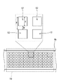
- FIG. 1 is a plan view schematically showing the solid material of the first embodiment.
- FIG. 2A is a cross-sectional view showing an example of the method for producing a solid material according to the first embodiment.
- FIG. 2B is a cross-sectional view showing an example of the method for producing a solid material according to the first embodiment.
- FIG. 2C is a cross-sectional view showing an example of the method for producing a solid material according to the first embodiment.
- FIG. 3 is a plan view schematically showing the solid material of the second embodiment.
- FIG. 4 is a plan view schematically showing the solid material of the third embodiment.
- FIG. 5 is a graph showing the relationship between the elastic modulus of the solid part of the sample and the thermal conductivity of the sample and the minimum dimension of the solid part of the sample.
- FIG. 6 is a load-displacement curve obtained by nanoindentation test on sample 1-A and reference sample.
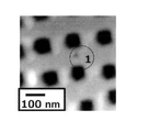
- FIG. 7A is a scanning probe microscope (SPM) image of the sample before measuring the elastic modulus.
- FIG. 7B is an SPM image showing the measurement points of the elastic modulus in the sample.
- FIG. 7C is an SPM image showing the measurement points of the elastic modulus in the sample.
- FIG. 7D is an SPM image showing the measurement points of the elastic modulus in the sample.
- FIG. 8A is a scanning electron microscope (SEM) image of the sample.
- FIG. 8B is an SPM image showing a state before measurement of the elastic modulus measurement point in the sample.
- FIG. 8C is an SPM image showing a state after measurement of the elastic modulus measurement point in the sample.
- FIG. 9A is an SEM image of the sample.
- FIG. 9B is an SPM image showing a state before measurement of the elastic modulus measurement point in the sample.
- FIG. 9C is an
- the thermal conductivity of a solid material such as an insulator and a semiconductor is determined by the dispersion relation of phonons in the solid material.
- the dispersion relation of phonons includes the relation between frequency and wave number or band structure.
- the frequency band of phonons carrying heat ranges from 100 GHz to 10 THz. This frequency band is a thermal band.
- the thermal conductivity of a solid material is determined by the dispersion relation of phonons in the thermal zone.
- the dispersion relation of phonons of the material can be adjusted by the periodic structure of the through holes.
- the thermal conductivity itself of a material such as a thin film base material can be adjusted.
- PBG phononic bandgap
- the thermal conductivity of the material can be significantly reduced. Phonons cannot exist inside the PBG. Therefore, the PBG formed in accordance with the heat band can be a barrier to heat conduction. Further, even in a frequency band other than the band corresponding to PBG, the slope of the phonon dispersion curve becomes smaller due to PBG. This reduces the group velocity of phonons and the thermal conductivity of the material. These matters greatly contribute to the reduction of the thermal conductivity of the material.
- the elastic modulus which is considered to be a physical property value peculiar to the material.
- a technique capable of reducing the elastic modulus of a solid material made of the same type of material can be developed, it is considered that high heat insulating performance can be imparted to the solid material.
- such a technique has not been developed as far as the present inventors know.
- the present inventors reduce the elastic modulus in the elastic deformation region, which is a stage before plastic deformation due to the solid material having a predetermined structure, and the effect of the reduction in the elastic modulus is solid. I got the idea that it might extend to the thermal modulus of the material. Based on such an idea, the present inventors have repeated trial and error to finally devise the solid material of the present disclosure.
- the present disclosure provides the following solid materials: It ’s a solid material, It has a plurality of recesses and a solid portion formed between the recesses, and has a three-dimensional structure that adjusts the thermal conductivity of the solid material by interacting with phonons.
- the minimum dimension of the solid portion between adjacent recesses in the plan view of the three-dimensional structure is 100 nanometers or less.
- the solid portion includes a portion having an elastic modulus of 80% or less of the elastic modulus of a reference sample prepared by using the same type of material as the material forming the solid portion without forming a plurality of recesses.
- the above solid material can exhibit high heat insulating performance because the solid part is configured as described above.
- FIG. 1 is a plan view showing the solid material 1a of the first embodiment.
- the solid material 1a comprises the three-dimensional structure 10.
- the three-dimensional structure 10 has a plurality of recesses 12 and a solid portion 14.
- the solid portion 14 is formed between the recesses 12.
- the three-dimensional structure 10 regulates the thermal conductivity of the solid material 1a by interacting with phonons.
- the minimum dimension N of the solid portion 14 between adjacent recesses 12 in the plan view of the three-dimensional structure 10 is 100 nm or less.
- the solid portion 14 includes a portion 14p having an elastic modulus Ep of 80% or less of the elastic modulus Er of the reference sample.
- the reference sample is a sample made of the same type of material as the material forming the solid portion 14 without forming a plurality of recesses.
- the reference sample is produced in the same manner as the solid material 1a except that it does not have a plurality of recesses, for example.
- the elastic modulus means Young's modulus.
- the solid material 1a tends to have high heat insulating performance.
- the elastic modulus Ep is adjusted as described above, the thermal conductivity of the solid material 1a tends to be low, and the solid material 1a tends to have high heat insulating performance.
- the portion 14p may be located between the adjacent recesses 12.
- the minimum dimension N of the solid portion 14 may be 90 nm or less, 85 nm or less, or 80 nm or less.
- the minimum dimension N may be 70 nm or less, 60 nm or less, 50 nm or less, or 40 nm or less.
- the minimum dimension N of the solid portion 14 is, for example, 1 nm or more.
- the elastic modulus Er of the reference sample and the elastic modulus Ep at the site 14p are determined according to, for example, the nanoindentation method.
- the test conditions for the nanoindentation method for example, the conditions described in Examples can be adopted.
- the elastic modulus Ep at the site 14p may be 75% or less, 70% or less, 65% or less, or 60% or less with respect to the elastic modulus Er. It may be 50% or less, or 40% or less.
- the elastic modulus Ep at the site 14p is, for example, 10% or more, 15% or more, 20% or more, 25% or more, or 30% with respect to the elastic modulus Er. It may be the above.
- the solid material 1a is, for example, a film having a thickness of 10 nm or more and 500 nm or less. As shown in FIG. 1, the solid material 1a has, for example, a rectangular shape in a plan view.
- the three-dimensional structure 10 is, for example, a phononic crystal. As shown in FIG. 1, the plurality of recesses 12 in the three-dimensional structure 10 are regularly arranged, for example, in the in-plane direction.
- the plurality of recesses 12 are arranged with a predetermined period P.
- the period P is, for example, 300 nm or less.
- the solid material 1a is more likely to have high heat insulating performance more reliably.
- the period P may be 280 nm or less, 260 nm or less, 250 nm or less, or 200 nm or less.
- the period P is, for example, 1 nm or more, may be 5 nm or more, or may be 10 nm or more.
- the shape of the recess 12 in the plan view of the three-dimensional structure 10 is not limited to a specific shape. As shown in FIG. 1, in the plan view of the three-dimensional structure 10, the recess 12 is, for example, circular.
- the plurality of recesses 12 are arranged, for example, in a specific direction with a period P.
- the opening of the recess 12 in a direction parallel to the specific direction has a predetermined dimension d.
- the dimension d and the period P satisfy, for example, the relationship of d / P ⁇ 0.5.
- the dimension d is, for example, 0.5 nm or more and 195 nm or less.
- a unit cell is formed by a regular arrangement of a plurality of recesses 12.
- This unit grid is not limited to a specific grid.
- the unit lattice composed of a regular arrangement of the plurality of recesses 12 is, for example, a hexagonal lattice.
- the unit lattice composed of a regular arrangement of the plurality of recesses 12 may be a square lattice, a rectangular lattice, or a face-centered rectangular lattice. You may.
- the phononic crystal in the three-dimensional structure 10 is, for example, a single crystal.
- the phononic crystal in the three-dimensional structure 10 may be, for example, a polycrystal.
- the phononic crystal has a plurality of domains in the plan view of the three-dimensional structure 10, and the phononic crystal in each domain is a single crystal.
- a polycrystalline phononic crystal is a complex of multiple phononic single crystals.
- the plurality of recesses 12 are regularly arranged in different directions.
- the orientation of the unit cell is the same in each domain.
- the shapes of the domains may be the same or different in the plan view of the three-dimensional structure 10.
- the size of each domain may be the same or different in the plan view of the three-dimensional structure 10.
- each domain in plan view is not limited to a specific shape.
- the shape of each domain in plan view is, for example, a polygon including triangles, squares, and rectangles, a circle, an ellipse, and a composite shape thereof.
- the shape of each domain in plan view may be amorphous.
- the number of domains contained in the phononic crystal in the three-dimensional structure 10 is not limited to a specific value.
- each domain in plan view of tertiary structure 10 is not limited to a particular value.
- each domain has, for example, an area of 25P 2 or more.
- the domain may have an area of 25P 2 or more.
- the domain has an area of 25 P 2 or more by adjusting the length of one side of the square to 5 ⁇ P or more.
- the plurality of recesses 12 form, for example, a plurality of through holes.
- the physical properties of the solid material 1a in the thickness direction of the film are less likely to vary.
- the opposite ends of the openings of the plurality of recesses 12 may be closed.
- the mechanical strength of the solid material 1a tends to be high.
- the depth of the recess 12 which is the dimension of the recess 12 in the thickness direction of the film, is not limited to a specific value.
- the ratio of the depth of the recess 12 to the dimension d of the opening of the recess 12 is, for example, 1 or more and 10 or less.
- the solid portion 14 of the solid material 1a may be formed of a single crystal, a polycrystal, or an amorphous material.
- the substance contained in the part 14p of the solid part 14 is not limited to a specific type of substance.
- the portion 14p is, for example, a semiconductor or an insulator.
- the site 14p may contain silicon.
- the elastic modulus of the site 14p is, for example, 100 GPa.
- the solid material 1a can be produced using silicon, and the solid material 1a tends to have high heat insulating performance.
- Silicon may be single crystal, polycrystal, or amorphous.
- the solid portion 14 has a plurality of different elastic moduli at a plurality of locations around a specific recess 12 in the plan view of the three-dimensional structure 10.
- the plurality of elastic moduli may be the same or different.
- the plurality of elastic moduli include, for example, a value in which the difference from the maximum value Emax of the plurality of elastic moduli is 10% or more of the maximum value Emax.
- the variation in elastic modulus tends to be large at a plurality of locations around the recess 12.
- Such a variation in elastic modulus can effectively contribute to a decrease in thermal conductivity in the solid material 1a. Therefore, the solid material 1a tends to have higher heat insulating performance more reliably.
- the silicon substrate 41 is prepared.
- the insulating film 42 containing SiO 2 is formed by thermal oxidation of one of the main surfaces of the silicon substrate 41 in the thickness direction. In this way, the base substrate 40 is obtained.
- the beam layer 43a is formed on the insulating film 42.
- the beam layer 43a can be formed by a known thin film forming method such as a chemical vapor deposition method (CVD method).
- the material constituting the beam layer 43a is not limited to a specific material.
- the material constituting the beam layer 43a is, for example, a material that changes to the first portion 13a and the second portion 13b by doping.
- the thickness of the beam layer 43a is not limited to a specific value.
- the thickness of the beam layer 43a is, for example, 10 nm or more and 500 nm or less.
- An SOI wafer may be used as a member provided with the base substrate 40 and the beam layer 43a.
- a plurality of recesses 12 regularly arranged in a plan view are formed in the beam layer 43a.
- the plurality of recesses 12 may be formed by, for example, electron beam lithography.
- the plurality of recesses 12 may be formed by, for example, block copolymer lithography.
- Block copolymer lithography is an advantageous method for producing polycrystalline phononic crystals in, for example, three-dimensional structure 10.
- a film-like solid material 1a is obtained.
- a recess 45 is formed below the solid material 1a to obtain a beam 43.
- the beam 43 is suspended above the recess 45. Both ends of the beam 43 are connected to, for example, the side surface of the recess 45.
- the solid material 1a is separated from the base substrate 40 by forming the recess 45.
- the conditions for selective etching are adjusted so that, for example, the plurality of recesses 12 form a plurality of through holes. As a result, the plurality of recesses 12 are connected to the recess 45.
- the elastic modulus of the site 14p in the solid material 1a can be determined, for example, by performing a nanoindentation test on the site corresponding to the site 14p in the state shown in FIG. 2B. In the state shown in FIG. 2B, a plurality of recesses 12 are formed in the beam layer 43a, and the entire beam layer 43a is in contact with the base substrate 40.
- the elastic modulus of the site 14p is determined by performing a nanoindentation test on the site 14p in a state where a sample obtained by cutting out a part of the solid material 1a shown in FIG. 2C is fixed to a substrate such as a silicon substrate. You may.
- FIG. 3 is a plan view showing the solid material 1b of the second embodiment.
- the solid material 1b is configured in the same manner as the solid material 1a except for a portion to be particularly described.
- the components of the solid material 1b that are the same as or corresponding to the components of the solid material 1a are designated by the same reference numerals, and detailed description thereof will be omitted.
- the description of solid material 1a also applies to solid material 1b, as long as it is not technically inconsistent.
- the plurality of recesses 12 of the solid material 1b are rectangular in the plan view of the three-dimensional structure 10. According to such a configuration, for example, when the solid material 1b is rectangular in a plan view, it is easy to arrange the plurality of recesses 12 in a wide range.
- FIG. 4 is a cross-sectional view showing the solid material 1c of the third embodiment.
- the solid material 1c is configured in the same manner as the solid material 1a except for a portion to be particularly described.
- the same components as those of the solid material 1a or the corresponding components of the solid material 1c are designated by the same reference numerals, and detailed description thereof will be omitted.
- the description of the solid material 1a also applies to the solid material 1c, as long as it is not technically inconsistent.
- the three-dimensional structure 10 includes the first site 13a, the second site 13b, and the third site 13c.
- the third site 13c is, for example, a site where the first site 13a and the second site 13b are joined.
- the solid material 1c can be produced, for example, by doping the beam 43 containing the solid material 1a produced as described above.
- the solid material 1c may be produced in the same manner as the solid material 1a except that the portion corresponding to the beam 43 in the beam layer 43a is doped in the state shown in FIG. 2A. In this case, doping is performed under the same conditions as the doping for producing the solid material 1c, and a reference sample is obtained.
- the first portion 13a and the second portion 13b are, for example, semiconductors having different conductive shapes from each other.
- the first portion 13a may have a conductive shape opposite to that of the second portion 13b.
- the conductive form of the semiconductor can be adjusted by doping.
- the first portion 13a may be a p-type semiconductor and the second portion 13b may be an n-type semiconductor.
- the first portion 13a and the second portion 13b can be formed by doping the beam 43 made of single crystal silicon. Processing process techniques for single crystal silicon have been established. Therefore, this example is excellent in manufacturability.
- the first site 13a has the first Seebeck coefficient.
- the second site 13b has, for example, a second Seebeck coefficient that is different from the first Seebeck coefficient.
- the first portion 13a, the second portion 13b, and the third portion 13c form, for example, a thermocouple element.
- the difference between the first Seebeck coefficient and the second Seebeck coefficient is not limited to a specific value. The difference is, for example, 10 ⁇ V / K or more.
- the Seebeck coefficient in the present specification means a value at 25 ° C.
- solid material of the present embodiment will be described in more detail with reference to the examples.
- the solid material of this embodiment is not limited to each of the embodiments shown in the following examples.
- a substrate having a silicon substrate, an insulating film, and a beam layer was prepared.
- This substrate was prepared by the Separation by Implanted Oxygen (SIMOX) method.
- the insulating film was formed by thermally oxidizing one main surface side of the silicon substrate and contained SiO 2 .
- the beam layer was a thin film of single crystal silicon, and the thickness of the beam layer was 100 nm.
- An insulating film was formed between the silicon substrate and the beam layer in the thickness direction of the silicon substrate.
- a plurality of through holes regularly arranged in the in-plane direction of the beam layer were formed by electron beam lithography or block copolymer lithography.
- samples 1-A, 2-A, 3-A, 4-A, 5-A, 6-A, and 7-A for measuring elastic modulus were obtained.
- the beam layer was in close contact with the insulating film as shown in FIG. 2B.
- the size d of the opening is shown in Table 1.
- a reference sample for elastic modulus measurement having a beam layer made of flat single crystal silicon was obtained in the same manner as the above sample except that a plurality of through holes were not formed.
- FIG. 5 shows the results of elastic modulus measurement of each sample.
- FIG. 5 shows the elastic modulus at a specific position on the surface of the beam layer of each sample as a relative value to the elastic modulus of the single crystal silicon forming the beam layer of the reference sample for measuring the elastic modulus.
- FIG. 6 shows the load-displacement curves obtained from the nanoindentation test for the elastic modulus measurement sample 1-A and the elastic modulus measurement reference sample.
- FIG. 6 shows a load-displacement curve obtained from a nanoindentation test at one location of the reference sample for elastic modulus measurement.
- Samples 1-B, 2-B, 3-B, 4-B, 5-B, 6-B, and 7-B were prepared.
- a beam was formed from the beam layer by selective etching, and a part of the insulating film was removed to form a recess. In these samples, the beam was suspended on a silicon substrate, as shown in FIG. 2C.
- the reference sample for elastic modulus measurement was similarly selectively etched to form beams and recesses, and a reference sample for thermal conductivity measurement was prepared.
- Sample 1-C for elastic modulus measurement Similar to Sample 1-A for elastic modulus measurement, except that the period P, the minimum dimension N of the solid part of the beam layer, and the dimension d of the opening of the through hole were adjusted to 150 nm, 60 nm, and 90 nm, respectively. Sample 1-C for measuring elastic modulus was prepared.
- FIG. 7A is an SPM image showing the surface of the elastic modulus measurement sample 1-C before the nanoindentation test.
- a diamond indenter was used for the nanoindentation test. The tip of the diamond indenter was processed to have a radius of curvature of 40 nm. The diamond indenter was pushed into the surface of the beam layer so that the load reached the maximum value of 20 ⁇ N over 5 seconds in the load control mode. Then, the load was maintained at a maximum value of 20 ⁇ N for 5 seconds, and then the load was reduced to 0 ⁇ N over 5 seconds for unloading.
- FIG. 7B is an SPM image showing the measurement points of the first nanoindentation test in the solid part of the beam layer. The point near the sign of "1" surrounded by the broken line circle corresponds to the measurement point.
- FIG. 7C is an SPM image showing the measurement points of the second nanoindentation test in the solid part of the beam layer. The point near the sign of "2" surrounded by the broken line circle corresponds to the measurement point.
- FIG. 7D is an SPM image showing the measurement point of the third nanoindentation test in the solid part of the beam layer. The point near the sign of "3" surrounded by the broken line circle corresponds to the measurement point. These measurement points are located around the opening of a specific through hole among the plurality of through holes.
- the elastic moduli of the solid part of the beam layer at the measurement points near the reference numerals “1”, “2”, and “3” were 64.4 GPa, 52.3 GPa, and 53.8 GPa, respectively.
- the elastic moduli at a plurality of locations around a specific through hole among the plurality of through holes do not show the same value but differ by 10% or more depending on the location. It is understood that such non-uniformity of elastic modulus of the beam layer, which is a continuum, contributes to the reduction of the thermal conductivity of the beam layer.
- Sample 1-D for elastic modulus measurement Similar to Sample 1-A for elastic modulus measurement, except that the period P, the minimum dimension N of the solid part of the beam layer, and the dimension d of the opening of the through hole were adjusted to 1297 nm, 104 nm, and 1193 nm, respectively.
- a grid-shaped sample 1-D for measuring elastic modulus was prepared.
- FIG. 8A is an SEM image showing the surface of the elastic modulus measurement sample 1-D.
- Example 1-E for elastic modulus measurement Similar to Sample 1-A for elastic modulus measurement, except that the period P, the minimum dimension N of the solid part of the beam layer, and the dimension d of the opening of the through hole were adjusted to 1259 nm, 67 nm, and 1192 nm, respectively.
- a grid-shaped sample 1-E for measuring elastic modulus was prepared.
- FIG. 9A is an SEM image showing the surface of the elastic modulus measurement sample 1-E.
- FIG. 8B is an SPM image showing the vicinity of a specific portion of the elastic modulus measurement sample 1-D before the nanoindentation test.
- FIG. 8C is an SPM image showing the vicinity of a specific portion of the elastic modulus measurement sample 1-D after the nanoindentation test. In FIG. 8C, a specific portion is surrounded by a broken line circle.
- FIG. 9B is an SPM image showing the vicinity of a specific portion of the elastic modulus measurement sample 1-E before the nanoindentation test.
- FIG. 9B is an SPM image showing the vicinity of a specific portion of the elastic modulus measurement sample 1-E before the nanoindentation test.
- FIG. 9C is an SPM image showing the vicinity of a specific portion of the elastic modulus measurement sample 1-E after the nanoindentation test.
- a specific portion is surrounded by a broken line circle.
- the surface observation method using SPM is advantageous in that the position of the indentation formed by the indentation can be accurately visualized in the nanoindentation test.
- FIG. 5 is a graph showing the relationship between the elastic modulus of the solid part of each sample and the thermal conductivity of each sample and the minimum dimension of the solid part of the sample.
- the vertical axis shows the elastic modulus of the solid portion of each sample and the thermal conductivity of each sample.
- the elastic modulus in the solid portion of each sample and the thermal conductivity of each sample are shown as relative values of the elastic modulus and the thermal conductivity of the single crystal silicon forming the beam layer of the reference sample for measuring the elastic modulus, respectively.
- the horizontal axis indicates the minimum dimension of the solid part in the sample. As shown in FIG.
- the difference between the elastic modulus of the solid part of the sample in which the minimum dimension N of the solid part of the beam layer is 150 nm or more and the elastic modulus of the single crystal silicon forming the beam layer of the reference sample for measuring the elastic modulus is not so large. not big.
- the thermal conductivity of the sample with a minimum dimension N of the solid part of the beam of 150 nm or more in the longitudinal direction is not so different from the thermal conductivity of the reference sample for measuring thermal conductivity in the longitudinal direction. ..
- the elastic modulus of the solid portion of the sample in which the minimum dimension N of the solid portion of the beam layer is 100 nm or less is lower than the elastic modulus of the single crystal silicon forming the beam layer of the reference sample for measuring the elastic modulus.
- the elastic modulus of the solid part of the sample is 35% of the elastic modulus of the single crystal silicon forming the beam layer of the reference sample for elastic modulus measurement.
- the thermal conductivity in the longitudinal direction of the beam of the sample in which the minimum dimension N of the solid portion of the beam is 100 nm or less is lower than the thermal conductivity in the longitudinal direction of the reference sample for measuring thermal conductivity.
- the thermal conductivity of the sample beam in the longitudinal direction is 41% of the thermal conductivity of the reference sample for measuring thermal conductivity in the longitudinal direction. It's just that. From these results, it was suggested that the elastic modulus, which is understood to be the physical property value peculiar to the material, can be adjusted by adjusting the minimum dimension N of the solid part. Further, the dependence of the elastic modulus of the solid portion on the minimum dimension N of the solid portion and the dependence of the thermal conductivity in the longitudinal direction of the beam on the minimum dimension N of the solid portion show the same tendency. Therefore, it is understood that the thermal conductivity in the longitudinal direction of the beam can be adjusted by adjusting the elastic modulus of the solid portion.
- the maximum displacement amount was only 7.2 nm in the load-displacement curve obtained from the nanoindentation test for the reference sample for elastic modulus measurement. Therefore, the elastic modulus of the single crystal silicon forming the beam layer of the reference sample for elastic modulus measurement was 150 GPa. This value is close to the bulk modulus value of single crystal silicon.
- the maximum displacement is 12.7 nm, and the elastic modulus at a specific point on the surface of the beam layer of this sample is 50 GPa. there were. As described above, it is understood that the elastic modulus of a specific part on the surface of the beam layer of the elastic modulus measurement sample 1-A is reduced to about one-third of the value close to the elastic modulus of the bulk of single crystal silicon. To.
- the elastic modulus of the solid part at the specific location in FIGS. 8C and 9C was 63.8 GPa and 34.0 GPa, respectively. rice field. It is understood that the elastic modulus of the material can be adjusted by microfabrication.
- the elastic modulus which was thought to be the physical property value peculiar to the substance, can be adjusted, and the thermal conductivity of the material can be adjusted by adjusting the elastic modulus. It was shown that it can be done.
- the above sample could be prepared for the first time by applying a material processing technique with a size of 100 nm or less, a precise elastic modulus evaluation technique for the material, and a thermal conductivity evaluation technique. It has been difficult to prepare such a sample by the prior art. These techniques are useful as techniques for further enhancing the heat insulating performance of the thermal infrared sensor.
- the infrared sensor of the present disclosure can be used for various purposes including the use of the infrared sensor.
Landscapes
- Engineering & Computer Science (AREA)
- General Engineering & Computer Science (AREA)
- Chemical & Material Sciences (AREA)
- Mechanical Engineering (AREA)
- General Physics & Mathematics (AREA)
- Physics & Mathematics (AREA)
- Nanotechnology (AREA)
- Materials Engineering (AREA)
- Condensed Matter Physics & Semiconductors (AREA)
- Crystallography & Structural Chemistry (AREA)
- Composite Materials (AREA)
- Spectroscopy & Molecular Physics (AREA)
- Inorganic Chemistry (AREA)
- Manufacturing & Machinery (AREA)
- Laminated Bodies (AREA)
- Crystals, And After-Treatments Of Crystals (AREA)
Priority Applications (1)
| Application Number | Priority Date | Filing Date | Title |
|---|---|---|---|
| US18/328,807 US20230313936A1 (en) | 2020-12-25 | 2023-06-05 | Solid material |
Applications Claiming Priority (2)
| Application Number | Priority Date | Filing Date | Title |
|---|---|---|---|
| JP2020-217806 | 2020-12-25 | ||
| JP2020217806A JP2022102826A (ja) | 2020-12-25 | 2020-12-25 | 固体材料 |
Related Child Applications (1)
| Application Number | Title | Priority Date | Filing Date |
|---|---|---|---|
| US18/328,807 Continuation US20230313936A1 (en) | 2020-12-25 | 2023-06-05 | Solid material |
Publications (1)
| Publication Number | Publication Date |
|---|---|
| WO2022138247A1 true WO2022138247A1 (ja) | 2022-06-30 |
Family
ID=82157861
Family Applications (1)
| Application Number | Title | Priority Date | Filing Date |
|---|---|---|---|
| PCT/JP2021/045642 Ceased WO2022138247A1 (ja) | 2020-12-25 | 2021-12-10 | 固体材料 |
Country Status (3)
| Country | Link |
|---|---|
| US (1) | US20230313936A1 (https=) |
| JP (1) | JP2022102826A (https=) |
| WO (1) | WO2022138247A1 (https=) |
Families Citing this family (1)
| Publication number | Priority date | Publication date | Assignee | Title |
|---|---|---|---|---|
| JP2022102827A (ja) * | 2020-12-25 | 2022-07-07 | パナソニックIpマネジメント株式会社 | 赤外線センサ |
Citations (4)
| Publication number | Priority date | Publication date | Assignee | Title |
|---|---|---|---|---|
| JP2017223644A (ja) * | 2016-06-13 | 2017-12-21 | パナソニックIpマネジメント株式会社 | 赤外線センサ |
| WO2019225058A1 (ja) * | 2018-05-22 | 2019-11-28 | パナソニックIpマネジメント株式会社 | 赤外線センサ及びフォノニック結晶体 |
| WO2020174732A1 (ja) * | 2019-02-28 | 2020-09-03 | パナソニックIpマネジメント株式会社 | 赤外線センサ及び赤外線センサアレイ |
| WO2020174731A1 (ja) * | 2019-02-28 | 2020-09-03 | パナソニックIpマネジメント株式会社 | 赤外線センサ、赤外線センサアレイ、及び赤外線センサの製造方法 |
-
2020
- 2020-12-25 JP JP2020217806A patent/JP2022102826A/ja active Pending
-
2021
- 2021-12-10 WO PCT/JP2021/045642 patent/WO2022138247A1/ja not_active Ceased
-
2023
- 2023-06-05 US US18/328,807 patent/US20230313936A1/en active Pending
Patent Citations (4)
| Publication number | Priority date | Publication date | Assignee | Title |
|---|---|---|---|---|
| JP2017223644A (ja) * | 2016-06-13 | 2017-12-21 | パナソニックIpマネジメント株式会社 | 赤外線センサ |
| WO2019225058A1 (ja) * | 2018-05-22 | 2019-11-28 | パナソニックIpマネジメント株式会社 | 赤外線センサ及びフォノニック結晶体 |
| WO2020174732A1 (ja) * | 2019-02-28 | 2020-09-03 | パナソニックIpマネジメント株式会社 | 赤外線センサ及び赤外線センサアレイ |
| WO2020174731A1 (ja) * | 2019-02-28 | 2020-09-03 | パナソニックIpマネジメント株式会社 | 赤外線センサ、赤外線センサアレイ、及び赤外線センサの製造方法 |
Also Published As
| Publication number | Publication date |
|---|---|
| JP2022102826A (ja) | 2022-07-07 |
| US20230313936A1 (en) | 2023-10-05 |
Similar Documents
| Publication | Publication Date | Title |
|---|---|---|
| Abramson et al. | Fabrication and characterization of a nanowire/polymer-based nanocomposite for a prototype thermoelectric device | |
| Gordon et al. | Size effects in mechanical deformation and fracture of cantilevered silicon nanowires | |
| Stan et al. | Ultimate bending strength of Si nanowires | |
| Palacio et al. | Atomic structure of epitaxial graphene sidewall nanoribbons: flat graphene, miniribbons, and the confinement gap | |
| Demami et al. | Silicon nanowires based resistors as gas sensors | |
| US20230309407A1 (en) | Infrared sensor | |
| Schmid | The impact of thermal annealing and adhesion film thickness on the resistivity and the agglomeration behavior of titanium/platinum thin films | |
| KR20140009182A (ko) | 낮은 열전도율을 위한 나노메쉬 포노닉 구조들 및 열전 에너지 변환 재료들 | |
| KR20100064360A (ko) | 수직으로 정렬된 si 와이어 어레이를 형성하기 위한 방법 및 구조 | |
| Ferrando-Villalba et al. | In-plane thermal conductivity of sub-20 nm thick suspended mono-crystalline Si layers | |
| Lee et al. | Focused ion beam-assisted manipulation of single and double β-SiC nanowires and their thermal conductivity measurements by the four-point-probe 3-ω method | |
| Liu et al. | Thermoelectric properties of holey silicon at elevated temperatures | |
| Ma et al. | Self-assembly growth of a multiferroic topological nanoisland array | |
| Gouder et al. | Investigation of microstructure and morphology for the Ge on porous silicon/Si substrate hetero-structure obtained by molecular beam epitaxy | |
| WO2022138247A1 (ja) | 固体材料 | |
| Wei et al. | Optimization and fabrication of MEMS suspended structures for nanoscale thermoelectric devices | |
| Nomura et al. | Mechanism of the reduced thermal conductivity of fishbone-type Si phononic crystal nanostructures | |
| Kallesøe et al. | Measurement of local Si‐nanowire growth kinetics using in situ transmission electron microscopy of heated cantilevers | |
| Ben Amor et al. | Si and Ge allotrope heterostructured nanowires: Experimental evaluation of the thermal conductivity reduction | |
| Huang et al. | Electromechanical failure of MoS 2 nanosheets | |
| Saeed et al. | Switching Dynamics and Improved Efficiency of Free‐Standing Antiferroelectric Capacitors | |
| JPWO2020174733A1 (ja) | 積層体及び結晶体 | |
| DelRio et al. | Near-theoretical fracture strengths in native and oxidized silicon nanowires | |
| Nguyen et al. | Piezojunction effect in heterojunctions under external bias for ultrasensitive strain sensing | |
| Amjadipour et al. | Fabrication of free-standing silicon carbide on silicon microstructures via massive silicon sublimation |
Legal Events
| Date | Code | Title | Description |
|---|---|---|---|
| 121 | Ep: the epo has been informed by wipo that ep was designated in this application |
Ref document number: 21910396 Country of ref document: EP Kind code of ref document: A1 |
|
| DPE1 | Request for preliminary examination filed after expiration of 19th month from priority date (pct application filed from 20040101) | ||
| NENP | Non-entry into the national phase |
Ref country code: DE |
|
| 122 | Ep: pct application non-entry in european phase |
Ref document number: 21910396 Country of ref document: EP Kind code of ref document: A1 |