WO2022130107A1 - 発光デバイス、発光装置、電子機器、および照明装置 - Google Patents
発光デバイス、発光装置、電子機器、および照明装置 Download PDFInfo
- Publication number
- WO2022130107A1 WO2022130107A1 PCT/IB2021/061348 IB2021061348W WO2022130107A1 WO 2022130107 A1 WO2022130107 A1 WO 2022130107A1 IB 2021061348 W IB2021061348 W IB 2021061348W WO 2022130107 A1 WO2022130107 A1 WO 2022130107A1
- Authority
- WO
- WIPO (PCT)
- Prior art keywords
- layer
- light emitting
- electrode
- emitting device
- abbreviation
- Prior art date
- Legal status (The legal status is an assumption and is not a legal conclusion. Google has not performed a legal analysis and makes no representation as to the accuracy of the status listed.)
- Ceased
Links
Images


















Classifications
-
- H—ELECTRICITY
- H10—SEMICONDUCTOR DEVICES; ELECTRIC SOLID-STATE DEVICES NOT OTHERWISE PROVIDED FOR
- H10K—ORGANIC ELECTRIC SOLID-STATE DEVICES
- H10K50/00—Organic light-emitting devices
- H10K50/10—OLEDs or polymer light-emitting diodes [PLED]
- H10K50/18—Carrier blocking layers
- H10K50/181—Electron blocking layers
-
- H—ELECTRICITY
- H05—ELECTRIC TECHNIQUES NOT OTHERWISE PROVIDED FOR
- H05B—ELECTRIC HEATING; ELECTRIC LIGHT SOURCES NOT OTHERWISE PROVIDED FOR; CIRCUIT ARRANGEMENTS FOR ELECTRIC LIGHT SOURCES, IN GENERAL
- H05B33/00—Electroluminescent light sources
- H05B33/12—Light sources with substantially two-dimensional [2D] radiating surfaces
-
- H—ELECTRICITY
- H05—ELECTRIC TECHNIQUES NOT OTHERWISE PROVIDED FOR
- H05B—ELECTRIC HEATING; ELECTRIC LIGHT SOURCES NOT OTHERWISE PROVIDED FOR; CIRCUIT ARRANGEMENTS FOR ELECTRIC LIGHT SOURCES, IN GENERAL
- H05B33/00—Electroluminescent light sources
- H05B33/12—Light sources with substantially two-dimensional [2D] radiating surfaces
- H05B33/22—Light sources with substantially two-dimensional [2D] radiating surfaces characterised by the chemical or physical composition or the arrangement of auxiliary dielectric or reflective layers
-
- H—ELECTRICITY
- H10—SEMICONDUCTOR DEVICES; ELECTRIC SOLID-STATE DEVICES NOT OTHERWISE PROVIDED FOR
- H10K—ORGANIC ELECTRIC SOLID-STATE DEVICES
- H10K50/00—Organic light-emitting devices
- H10K50/10—OLEDs or polymer light-emitting diodes [PLED]
- H10K50/14—Carrier transporting layers
- H10K50/15—Hole transporting layers
- H10K50/157—Hole transporting layers between the light-emitting layer and the cathode
-
- H—ELECTRICITY
- H10—SEMICONDUCTOR DEVICES; ELECTRIC SOLID-STATE DEVICES NOT OTHERWISE PROVIDED FOR
- H10K—ORGANIC ELECTRIC SOLID-STATE DEVICES
- H10K50/00—Organic light-emitting devices
- H10K50/80—Constructional details
- H10K50/805—Electrodes
- H10K50/82—Cathodes
- H10K50/826—Multilayers, e.g. opaque multilayers
-
- H—ELECTRICITY
- H10—SEMICONDUCTOR DEVICES; ELECTRIC SOLID-STATE DEVICES NOT OTHERWISE PROVIDED FOR
- H10K—ORGANIC ELECTRIC SOLID-STATE DEVICES
- H10K50/00—Organic light-emitting devices
- H10K50/80—Constructional details
- H10K50/84—Passivation; Containers; Encapsulations
- H10K50/844—Encapsulations
-
- H—ELECTRICITY
- H10—SEMICONDUCTOR DEVICES; ELECTRIC SOLID-STATE DEVICES NOT OTHERWISE PROVIDED FOR
- H10K—ORGANIC ELECTRIC SOLID-STATE DEVICES
- H10K59/00—Integrated devices, or assemblies of multiple devices, comprising at least one organic light-emitting element covered by group H10K50/00
- H10K59/10—OLED displays
- H10K59/12—Active-matrix OLED [AMOLED] displays
- H10K59/122—Pixel-defining structures or layers, e.g. banks
-
- H—ELECTRICITY
- H10—SEMICONDUCTOR DEVICES; ELECTRIC SOLID-STATE DEVICES NOT OTHERWISE PROVIDED FOR
- H10K—ORGANIC ELECTRIC SOLID-STATE DEVICES
- H10K2101/00—Properties of the organic materials covered by group H10K85/00
- H10K2101/50—Oxidation-reduction potentials, e.g. excited state redox potentials
-
- H—ELECTRICITY
- H10—SEMICONDUCTOR DEVICES; ELECTRIC SOLID-STATE DEVICES NOT OTHERWISE PROVIDED FOR
- H10K—ORGANIC ELECTRIC SOLID-STATE DEVICES
- H10K50/00—Organic light-emitting devices
- H10K50/10—OLEDs or polymer light-emitting diodes [PLED]
- H10K50/11—OLEDs or polymer light-emitting diodes [PLED] characterised by the electroluminescent [EL] layers
- H10K50/125—OLEDs or polymer light-emitting diodes [PLED] characterised by the electroluminescent [EL] layers specially adapted for multicolour light emission, e.g. for emitting white light
-
- H—ELECTRICITY
- H10—SEMICONDUCTOR DEVICES; ELECTRIC SOLID-STATE DEVICES NOT OTHERWISE PROVIDED FOR
- H10K—ORGANIC ELECTRIC SOLID-STATE DEVICES
- H10K50/00—Organic light-emitting devices
- H10K50/10—OLEDs or polymer light-emitting diodes [PLED]
- H10K50/14—Carrier transporting layers
- H10K50/15—Hole transporting layers
-
- H—ELECTRICITY
- H10—SEMICONDUCTOR DEVICES; ELECTRIC SOLID-STATE DEVICES NOT OTHERWISE PROVIDED FOR
- H10K—ORGANIC ELECTRIC SOLID-STATE DEVICES
- H10K59/00—Integrated devices, or assemblies of multiple devices, comprising at least one organic light-emitting element covered by group H10K50/00
- H10K59/30—Devices specially adapted for multicolour light emission
- H10K59/35—Devices specially adapted for multicolour light emission comprising red-green-blue [RGB] subpixels
Definitions
- one conductive film may be plural, for example, when a part of the wiring functions as an electrode. In some cases, it also has the functions of the components of.
- connection includes the case where one conductive film has the functions of a plurality of components in combination.
- an excited complex made of two types of host materials can be formed.
- Organic metal complex having, tris [3-methyl-1- (2-methylphenyl) -5-phenyl-1H-1,2,4-triazolat] iridium (III) (abbreviation: [Ir (Mptz1-mp) 3 ) ]), 1H-triazole such as Tris (1-methyl-5-phenyl-3-propyl-1H-1,2,4-triazolat) iridium (III) (abbreviation: [Ir (Prptz1-Me) 3 ]).
- Platinum complexes such as Tris (1,3-diphenyl-1,3-propanedionat) (monophenanthroline) Europium (III) (abbreviation: [Eu (DBM) 3 (Phen)]), Tris [1- (2) -Tenoyl) -3,3,3-trifluoroacetonato] (monophenanthroline) Europium (III) (abbreviation: [Eu (TTA) 3 (Phen)]) and other rare earth metal complexes.
- the electron-transporting material examples include 2- [3'-(dibenzothiophen-4-yl) biphenyl-3-yl] dibenzo [f, h] quinoxalin (abbreviation: 2mDBTBPDBq-II), 5- [.
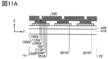
- the light emitting device 550G has an electrode 551G, an electrode 552, an EL layer 103G, an oxidation resistant layer 105G, and a block layer 107.
- the specific configuration of each layer is as shown in the first embodiment.
- the EL layer 103G has a laminated structure including a plurality of layers having different functions including the light emitting layer 113G.
- the oxidation resistant layer 105G is included in the EL layer 103G.
- FIG. 3A among the layers included in the EL layer 103G including the light emitting layer 113G, only the hole injection / transport layer 104G and the oxidation resistant layer 105G are shown, but the present invention is not limited to this.
- the hole injection / transport layer 104G indicates a layer having the functions of the hole injection layer and the hole transport layer shown in the first embodiment, and may have a laminated structure.
- the hole injection layer included in the hole transport region located between the anode and the light emitting layer is often formed as a layer common to adjacent light emitting devices because the conductivity is often high. , May cause crosstalk. Therefore, by providing a gap 580 between each EL layer as shown in this configuration example, it is possible to suppress the occurrence of crosstalk that occurs between adjacent light emitting devices.
- the metal oxide examples include oxides of metals belonging to Group 4 to Group 8 in the Periodic Table of the Elements. Specific examples thereof include vanadium oxide, niobium oxide, tantalum oxide, chromium oxide, molybdenum oxide, tungsten oxide, manganese oxide, and renium oxide. Further, as the organic compound, a material listed as a hole transporting material can be used.
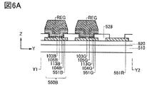
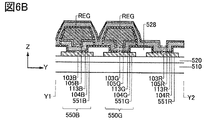
- the EL layer 103R (light emitting layer 113R, hole injection / transport layer) is placed on the resist REG, the electrode 551R, and the partition wall 528.
- 104R and an oxidation resistant layer 105R are included.
- a vacuum vapor deposition method is used to form an EL layer 103R on the electrode 551R, the resist REG, and the partition wall 528 so as to cover them.
- the oxidation-resistant layer 105R is formed by using a composite material containing a metal oxide and an organic compound (hole transporting material), similarly to the oxidation-resistant layer 105B.
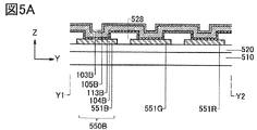
- Exposure of the surface of the electrode to etching can cause damage to the surface of the electrode. Further, by forming a light emitting device using an electrode having a damaged surface, the characteristics of the light emitting device may be deteriorated. The degree to which the surface condition of the electrode affects the characteristics of the light emitting device depends on the structure of the light emitting device, the material used, and the like. Comparing the light emitting device 550B, the light emitting device 550G, and the light emitting device 550R, it may be the light emitting device 550B that the surface state of the electrode most easily affects the characteristics.
- the light emitting device 550B, the light emitting device 550G, and the light emitting device 550R have the device structure shown in the first embodiment. In particular, the case where the EL layer 103 in the structure shown in FIG. 2A is different for each light emitting device is shown.
- the EL layer 103P and the electrode 552 more specifically, the hole injection / transport layer 104P and the electrode 552, the EL layer 103Q and the electrode 552, and more specifically the EL layer 103Q, which the EL layer 103P has. It is possible to prevent the hole injection / transport layer 104Q and the electrode 552, or the charge generation layer 106B and the electrode 552, from being electrically short-circuited.
- the block layer 107 is formed so as to cover the EL layer 103P, the EL layer 103Q, and the charge generation layer 106R, which are formed on the electrode 551R.
- the EL layer 103P, the EL layer 103Q, and the charge generation layer 106R have side surfaces (or ends). Therefore, the block layer 107 is formed in contact with the side surfaces (or ends) of the EL layer 103P, the EL layer 103Q, and the charge generation layer 106R. Thereby, it is possible to suppress the invasion of oxygen and water or their constituent elements from the side surfaces of the EL layer 103P, the EL layer 103Q, and the charge generation layer 106R, respectively.
- the hole transporting material shown in the first embodiment can be used for the block layer 107.
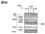
- FIG. 9B shows the configuration of the light emitting device 550B when the light emitting device 550B, the light emitting device 550G, and the light emitting device 550R are light emitting devices that emit white light.
- the EL layer 103P and the EL layer 103Q are laminated on the electrode 551B with the charge generation layer 106B interposed therebetween. Further, the EL layer 103P has a light emitting layer 113B that emits, for example, a blue light EL (1) as a light emitting layer 113P, and the EL layer 103Q emits, for example, a green light EL (2) as a light emitting layer 113Q. It has a light emitting layer 113G to emit light and a light emitting layer 113R to emit red light EL (3).
- the electrode 552 is formed on the block layer 107.
- the electrodes 552 include an EL layer 103P (including a light emitting layer 113P and a hole injection / transport layer 104P), a charge generation layer (106B, 106G, 106R), and an EL layer 103Q (light emitting layer 113Q,) via the block layer 107. It has a structure in contact with the side surface of the hole injection / transport layer 104Q and the oxidation resistant layer 105Q).
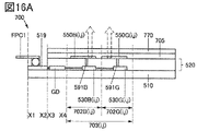
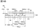
- a plurality of pixels can be used for the pixel 703 (i, j). For example, it is possible to use a plurality of pixels that display colors having different hues from each other. It should be noted that each of the plurality of pixels can be paraphrased as a sub-pixel. Alternatively, a plurality of sub-pixels can be combined into a set and paraphrased as a pixel.
- the drive circuit GD has a function of supplying a first selection signal and a second selection signal.
- the drive circuit GD is electrically connected to the conductive film G1 (i) to supply a first selection signal, and is electrically connected to the conductive film G2 (i) to supply a second selection signal.
- the drive circuit SD has a function of supplying an image signal and a control signal, and the control signal includes a first level and a second level.
- the drive circuit SD is electrically connected to the conductive film S1g (j) to supply an image signal, and is electrically connected to the conductive film S2g (j) to supply a control signal.
- each pixel circuit included in the functional layer 520 is each light emitting device (for example) formed on the functional layer 520.
- the light emitting device 550B (i, j) shown in FIG. 16A, and the light emitting device 550G (i, j)) are electrically connected.
- a second insulating layer 705 is provided on the functional layer 520 and each light emitting device, and the second insulating layer 705 has a function of bonding the second substrate 770 and the functional layer 520.
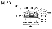
- the conductive film 512A has either the function of the source electrode or the function of the drain electrode, and the conductive film 512B has the function of the source electrode or the function of the drain electrode.
- an oxide semiconductor can be used for the semiconductor film 508.
- an oxide semiconductor containing indium, an oxide semiconductor containing indium, gallium and zinc, or an oxide semiconductor containing indium, gallium, zinc and tin can be used for the semiconductor film 508.
- the active matrix type light emitting device has been described with reference to FIGS. 16A and 16B, the configuration of the light emitting device shown in the first embodiment may be applied to the passive matrix type light emitting device shown in FIG.
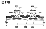
- FIG. 17A is a perspective view showing a passive matrix type light emitting device
- FIG. 17B is a cross-sectional view of FIG. 17A cut by XY.
- an EL layer 955 is provided between the electrodes 952 and the electrodes 956 on the substrate 951.
- the end of the electrode 952 is covered with an insulating layer 953.
- a partition wall layer 954 is provided on the insulating layer 953.
- the side wall of the partition wall layer 954 has an inclination such that the distance between one side wall and the other side wall becomes narrower as it gets closer to the substrate surface.
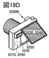
- FIG. 19B shows an electronic device in which the remote controller can be the input unit 5240.
- An example is a television system.
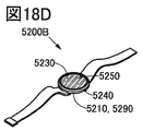
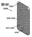
- information can be received from a broadcasting station or the Internet and displayed on the display unit 5230.
- the user can be photographed using the detection unit 5250.
- the user's video can be transmitted.
- the viewing history of the user can be acquired and provided to the cloud service.
- the recommendation information can be acquired from the cloud service and displayed on the display unit 5230.
- the program or video can be displayed based on the recommendation information.
- it has a function of changing the display method according to the illuminance of the usage environment. As a result, the image can be displayed on the display unit 5230 so that it can be suitably used even when it is exposed to strong external light that is inserted indoors on a sunny day.
- the EL layer 403 is formed on the first electrode 401.
- the EL layer 403 corresponds to the configuration of the EL layer 103 in the first embodiment, or the configuration in which the EL layers 103a, 103b, 103c and the charge generation layer 106 (106a, 106b) are combined. Please refer to the description for these configurations.
Landscapes
- Physics & Mathematics (AREA)
- Optics & Photonics (AREA)
- Engineering & Computer Science (AREA)
- Microelectronics & Electronic Packaging (AREA)
- Electroluminescent Light Sources (AREA)
- Devices For Indicating Variable Information By Combining Individual Elements (AREA)
Priority Applications (3)
| Application Number | Priority Date | Filing Date | Title |
|---|---|---|---|
| JP2022569314A JP7726916B2 (ja) | 2020-12-18 | 2021-12-06 | 発光デバイス、発光装置、電子機器、および照明装置 |
| US18/266,908 US20240065024A1 (en) | 2020-12-18 | 2021-12-06 | Light-Emitting Device, Light-Emitting Apparatus, Electronic Device, and Lighting Device |
| JP2025132344A JP2025159060A (ja) | 2020-12-18 | 2025-08-07 | 発光装置、電子機器および照明装置 |
Applications Claiming Priority (2)
| Application Number | Priority Date | Filing Date | Title |
|---|---|---|---|
| JP2020210174 | 2020-12-18 | ||
| JP2020-210174 | 2020-12-18 |
Publications (1)
| Publication Number | Publication Date |
|---|---|
| WO2022130107A1 true WO2022130107A1 (ja) | 2022-06-23 |
Family
ID=82058968
Family Applications (1)
| Application Number | Title | Priority Date | Filing Date |
|---|---|---|---|
| PCT/IB2021/061348 Ceased WO2022130107A1 (ja) | 2020-12-18 | 2021-12-06 | 発光デバイス、発光装置、電子機器、および照明装置 |
Country Status (3)
| Country | Link |
|---|---|
| US (1) | US20240065024A1 (https=) |
| JP (2) | JP7726916B2 (https=) |
| WO (1) | WO2022130107A1 (https=) |
Families Citing this family (1)
| Publication number | Priority date | Publication date | Assignee | Title |
|---|---|---|---|---|
| KR20220111814A (ko) * | 2021-02-02 | 2022-08-10 | 삼성디스플레이 주식회사 | 표시장치 |
Citations (5)
| Publication number | Priority date | Publication date | Assignee | Title |
|---|---|---|---|---|
| JP2008251270A (ja) * | 2007-03-29 | 2008-10-16 | Dainippon Printing Co Ltd | 有機エレクトロルミネッセンス素子およびその製造方法 |
| JP2011029322A (ja) * | 2009-07-23 | 2011-02-10 | Sony Corp | 表示装置および表示装置の製造方法 |
| JP2012028318A (ja) * | 2010-06-25 | 2012-02-09 | Semiconductor Energy Lab Co Ltd | 発光素子、発光装置、ディスプレイ及び電子機器 |
| JP2014022221A (ja) * | 2012-07-19 | 2014-02-03 | Panasonic Corp | 表示パネルの製造方法 |
| JP2020025137A (ja) * | 2009-09-04 | 2020-02-13 | 株式会社半導体エネルギー研究所 | 発光素子及び発光装置 |
Family Cites Families (2)
| Publication number | Priority date | Publication date | Assignee | Title |
|---|---|---|---|---|
| JP5233598B2 (ja) | 2008-11-05 | 2013-07-10 | 凸版印刷株式会社 | 有機elディスプレイパネル及びその製造方法 |
| JP2013134847A (ja) | 2011-12-26 | 2013-07-08 | Panasonic Corp | 表示パネルの製造方法および表示パネル |
-
2021
- 2021-12-06 US US18/266,908 patent/US20240065024A1/en active Pending
- 2021-12-06 WO PCT/IB2021/061348 patent/WO2022130107A1/ja not_active Ceased
- 2021-12-06 JP JP2022569314A patent/JP7726916B2/ja active Active
-
2025
- 2025-08-07 JP JP2025132344A patent/JP2025159060A/ja active Pending
Patent Citations (5)
| Publication number | Priority date | Publication date | Assignee | Title |
|---|---|---|---|---|
| JP2008251270A (ja) * | 2007-03-29 | 2008-10-16 | Dainippon Printing Co Ltd | 有機エレクトロルミネッセンス素子およびその製造方法 |
| JP2011029322A (ja) * | 2009-07-23 | 2011-02-10 | Sony Corp | 表示装置および表示装置の製造方法 |
| JP2020025137A (ja) * | 2009-09-04 | 2020-02-13 | 株式会社半導体エネルギー研究所 | 発光素子及び発光装置 |
| JP2012028318A (ja) * | 2010-06-25 | 2012-02-09 | Semiconductor Energy Lab Co Ltd | 発光素子、発光装置、ディスプレイ及び電子機器 |
| JP2014022221A (ja) * | 2012-07-19 | 2014-02-03 | Panasonic Corp | 表示パネルの製造方法 |
Also Published As
| Publication number | Publication date |
|---|---|
| US20240065024A1 (en) | 2024-02-22 |
| JP2025159060A (ja) | 2025-10-17 |
| JPWO2022130107A1 (https=) | 2022-06-23 |
| JP7726916B2 (ja) | 2025-08-20 |
Similar Documents
| Publication | Publication Date | Title |
|---|---|---|
| JP6690919B2 (ja) | 発光装置、照明装置、表示装置、及び電子機器 | |
| US12581796B2 (en) | Light-emitting device, light-emitting apparatus, electronic device, and lighting device | |
| JP2023007468A (ja) | 発光デバイスおよび発光装置 | |
| JP2026050469A (ja) | 発光デバイス | |
| JP2025159060A (ja) | 発光装置、電子機器および照明装置 | |
| WO2023281330A1 (ja) | 受光デバイス、受発光装置、電子機器 | |
| US20240155863A1 (en) | Light-Emitting Device, Light-Emitting Apparatus, Electronic Appliance, and Lighting Device | |
| JP2022159081A (ja) | 発光デバイス用混合材料 | |
| JP2022132168A (ja) | 混合材料 | |
| JP2022167859A (ja) | 発光デバイス、発光装置、電子機器および照明装置 | |
| JP2022159214A (ja) | 有機化合物、発光デバイス、発光装置、電子機器および照明装置 | |
| US20240138259A1 (en) | Organic compound, light-emitting device, light-emitting apparatus, electronic device, and lighting device | |
| US20240121979A1 (en) | Light-Emitting Device, Light-Emitting Apparatus, Electronic Appliance, and Lighting Device | |
| US20240130228A1 (en) | Light-Emitting Device, Light-Emitting Apparatus, Electronic Appliance, and Lighting Device | |
| US20240315066A1 (en) | Light-Emitting Device, Light-Emitting Apparatus, Electronic Appliance, and Lighting Device | |
| JP2022115848A (ja) | 有機化合物、発光デバイス、発光装置、電子機器および照明装置 | |
| JP2024046630A (ja) | 高分子化合物、発光デバイス、発光装置、電子機器、および照明装置 | |
| KR20230014062A (ko) | 발광 디바이스, 발광 장치, 수발광 장치, 전자 기기, 및 조명 장치 |
Legal Events
| Date | Code | Title | Description |
|---|---|---|---|
| 121 | Ep: the epo has been informed by wipo that ep was designated in this application |
Ref document number: 21905920 Country of ref document: EP Kind code of ref document: A1 |
|
| ENP | Entry into the national phase |
Ref document number: 2022569314 Country of ref document: JP Kind code of ref document: A |
|
| WWE | Wipo information: entry into national phase |
Ref document number: 18266908 Country of ref document: US |
|
| NENP | Non-entry into the national phase |
Ref country code: DE |
|
| 122 | Ep: pct application non-entry in european phase |
Ref document number: 21905920 Country of ref document: EP Kind code of ref document: A1 |