WO2022123816A1 - Piezoelectric vibrator, piezoelectric oscillator, and method for making piezoelectric vibrator - Google Patents
Piezoelectric vibrator, piezoelectric oscillator, and method for making piezoelectric vibrator Download PDFInfo
- Publication number
- WO2022123816A1 WO2022123816A1 PCT/JP2021/025550 JP2021025550W WO2022123816A1 WO 2022123816 A1 WO2022123816 A1 WO 2022123816A1 JP 2021025550 W JP2021025550 W JP 2021025550W WO 2022123816 A1 WO2022123816 A1 WO 2022123816A1
- Authority
- WO
- WIPO (PCT)
- Prior art keywords
- piezoelectric
- crystal
- electrode
- vibrating
- extraction electrode
- Prior art date
Links
- 238000000034 method Methods 0.000 title claims abstract description 16
- 238000000605 extraction Methods 0.000 claims abstract description 94
- 230000005284 excitation Effects 0.000 claims abstract description 74
- 239000000758 substrate Substances 0.000 claims description 44
- VYPSYNLAJGMNEJ-UHFFFAOYSA-N Silicium dioxide Chemical group O=[Si]=O VYPSYNLAJGMNEJ-UHFFFAOYSA-N 0.000 claims description 28
- 239000000463 material Substances 0.000 claims description 23
- 235000012239 silicon dioxide Nutrition 0.000 claims description 21
- 239000004020 conductor Substances 0.000 claims description 18
- 239000010453 quartz Substances 0.000 claims description 18
- 238000004519 manufacturing process Methods 0.000 claims description 9
- 238000005304 joining Methods 0.000 claims description 5
- 239000000377 silicon dioxide Substances 0.000 claims description 3
- 239000013078 crystal Substances 0.000 abstract description 240
- 238000009413 insulation Methods 0.000 abstract description 3
- 230000035882 stress Effects 0.000 description 35
- 238000012986 modification Methods 0.000 description 18
- 230000004048 modification Effects 0.000 description 18
- 239000011521 glass Substances 0.000 description 13
- 239000003822 epoxy resin Substances 0.000 description 12
- 229920000647 polyepoxide Polymers 0.000 description 12
- 230000001070 adhesive effect Effects 0.000 description 8
- PXHVJJICTQNCMI-UHFFFAOYSA-N Nickel Chemical compound [Ni] PXHVJJICTQNCMI-UHFFFAOYSA-N 0.000 description 6
- 239000000853 adhesive Substances 0.000 description 6
- 239000007789 gas Substances 0.000 description 6
- 238000005530 etching Methods 0.000 description 5
- 239000010931 gold Substances 0.000 description 5
- 239000000919 ceramic Substances 0.000 description 4
- 239000010408 film Substances 0.000 description 4
- 230000000149 penetrating effect Effects 0.000 description 4
- 229920005989 resin Polymers 0.000 description 4
- 239000011347 resin Substances 0.000 description 4
- 229910052814 silicon oxide Inorganic materials 0.000 description 4
- 239000004593 Epoxy Substances 0.000 description 3
- 229910004298 SiO 2 Inorganic materials 0.000 description 3
- 229910045601 alloy Inorganic materials 0.000 description 3
- 239000000956 alloy Substances 0.000 description 3
- PCHJSUWPFVWCPO-UHFFFAOYSA-N gold Chemical compound [Au] PCHJSUWPFVWCPO-UHFFFAOYSA-N 0.000 description 3
- 229910052737 gold Inorganic materials 0.000 description 3
- 230000008018 melting Effects 0.000 description 3
- 238000002844 melting Methods 0.000 description 3
- 229920003986 novolac Polymers 0.000 description 3
- 230000010355 oscillation Effects 0.000 description 3
- 229910000679 solder Inorganic materials 0.000 description 3
- 239000010936 titanium Substances 0.000 description 3
- LEONUFNNVUYDNQ-UHFFFAOYSA-N vanadium atom Chemical compound [V] LEONUFNNVUYDNQ-UHFFFAOYSA-N 0.000 description 3
- XEEYBQQBJWHFJM-UHFFFAOYSA-N Iron Chemical compound [Fe] XEEYBQQBJWHFJM-UHFFFAOYSA-N 0.000 description 2
- 229910052581 Si3N4 Inorganic materials 0.000 description 2
- XUIMIQQOPSSXEZ-UHFFFAOYSA-N Silicon Chemical compound [Si] XUIMIQQOPSSXEZ-UHFFFAOYSA-N 0.000 description 2
- RTAQQCXQSZGOHL-UHFFFAOYSA-N Titanium Chemical compound [Ti] RTAQQCXQSZGOHL-UHFFFAOYSA-N 0.000 description 2
- 229910052782 aluminium Inorganic materials 0.000 description 2
- XAGFODPZIPBFFR-UHFFFAOYSA-N aluminium Chemical compound [Al] XAGFODPZIPBFFR-UHFFFAOYSA-N 0.000 description 2
- IISBACLAFKSPIT-UHFFFAOYSA-N bisphenol A Chemical compound C=1C=C(O)C=CC=1C(C)(C)C1=CC=C(O)C=C1 IISBACLAFKSPIT-UHFFFAOYSA-N 0.000 description 2
- PXKLMJQFEQBVLD-UHFFFAOYSA-N bisphenol F Chemical compound C1=CC(O)=CC=C1CC1=CC=C(O)C=C1 PXKLMJQFEQBVLD-UHFFFAOYSA-N 0.000 description 2
- 239000010949 copper Substances 0.000 description 2
- 238000001312 dry etching Methods 0.000 description 2
- 230000000694 effects Effects 0.000 description 2
- 230000005684 electric field Effects 0.000 description 2
- LNEPOXFFQSENCJ-UHFFFAOYSA-N haloperidol Chemical compound C1CC(O)(C=2C=CC(Cl)=CC=2)CCN1CCCC(=O)C1=CC=C(F)C=C1 LNEPOXFFQSENCJ-UHFFFAOYSA-N 0.000 description 2
- 238000010438 heat treatment Methods 0.000 description 2
- 229910052751 metal Inorganic materials 0.000 description 2
- 239000002184 metal Substances 0.000 description 2
- 229910052759 nickel Inorganic materials 0.000 description 2
- 230000002093 peripheral effect Effects 0.000 description 2
- 239000012071 phase Substances 0.000 description 2
- 229910052710 silicon Inorganic materials 0.000 description 2
- 239000010703 silicon Substances 0.000 description 2
- HQVNEWCFYHHQES-UHFFFAOYSA-N silicon nitride Chemical compound N12[Si]34N5[Si]62N3[Si]51N64 HQVNEWCFYHHQES-UHFFFAOYSA-N 0.000 description 2
- 238000004544 sputter deposition Methods 0.000 description 2
- 238000000427 thin-film deposition Methods 0.000 description 2
- 229910052719 titanium Inorganic materials 0.000 description 2
- 229910052720 vanadium Inorganic materials 0.000 description 2
- 238000001039 wet etching Methods 0.000 description 2
- QTWJRLJHJPIABL-UHFFFAOYSA-N 2-methylphenol;3-methylphenol;4-methylphenol Chemical compound CC1=CC=C(O)C=C1.CC1=CC=CC(O)=C1.CC1=CC=CC=C1O QTWJRLJHJPIABL-UHFFFAOYSA-N 0.000 description 1
- RYGMFSIKBFXOCR-UHFFFAOYSA-N Copper Chemical compound [Cu] RYGMFSIKBFXOCR-UHFFFAOYSA-N 0.000 description 1
- KRHYYFGTRYWZRS-UHFFFAOYSA-N Fluorane Chemical compound F KRHYYFGTRYWZRS-UHFFFAOYSA-N 0.000 description 1
- ZOKXTWBITQBERF-UHFFFAOYSA-N Molybdenum Chemical compound [Mo] ZOKXTWBITQBERF-UHFFFAOYSA-N 0.000 description 1
- ISWSIDIOOBJBQZ-UHFFFAOYSA-N Phenol Chemical compound OC1=CC=CC=C1 ISWSIDIOOBJBQZ-UHFFFAOYSA-N 0.000 description 1
- BQCADISMDOOEFD-UHFFFAOYSA-N Silver Chemical compound [Ag] BQCADISMDOOEFD-UHFFFAOYSA-N 0.000 description 1
- QYIJPFYCTROKTM-UHFFFAOYSA-N [Sn].P(O)(O)(O)=O Chemical compound [Sn].P(O)(O)(O)=O QYIJPFYCTROKTM-UHFFFAOYSA-N 0.000 description 1
- 230000032683 aging Effects 0.000 description 1
- 125000002723 alicyclic group Chemical group 0.000 description 1
- 230000001588 bifunctional effect Effects 0.000 description 1
- 239000011230 binding agent Substances 0.000 description 1
- KGBXLFKZBHKPEV-UHFFFAOYSA-N boric acid Chemical compound OB(O)O KGBXLFKZBHKPEV-UHFFFAOYSA-N 0.000 description 1
- 239000004327 boric acid Substances 0.000 description 1
- 239000003990 capacitor Substances 0.000 description 1
- 229910017052 cobalt Inorganic materials 0.000 description 1
- 239000010941 cobalt Substances 0.000 description 1
- GUTLYIVDDKVIGB-UHFFFAOYSA-N cobalt atom Chemical compound [Co] GUTLYIVDDKVIGB-UHFFFAOYSA-N 0.000 description 1
- 238000004891 communication Methods 0.000 description 1
- 229910052802 copper Inorganic materials 0.000 description 1
- 229930003836 cresol Natural products 0.000 description 1
- 125000000623 heterocyclic group Chemical group 0.000 description 1
- 229910000040 hydrogen fluoride Inorganic materials 0.000 description 1
- 239000011261 inert gas Substances 0.000 description 1
- 229910000833 kovar Inorganic materials 0.000 description 1
- 239000000155 melt Substances 0.000 description 1
- 239000007769 metal material Substances 0.000 description 1
- 150000002739 metals Chemical class 0.000 description 1
- 238000010295 mobile communication Methods 0.000 description 1
- 229910052750 molybdenum Inorganic materials 0.000 description 1
- 239000011733 molybdenum Substances 0.000 description 1
- 230000003287 optical effect Effects 0.000 description 1
- AFEQENGXSMURHA-UHFFFAOYSA-N oxiran-2-ylmethanamine Chemical compound NCC1CO1 AFEQENGXSMURHA-UHFFFAOYSA-N 0.000 description 1
- 229910052709 silver Inorganic materials 0.000 description 1
- 239000004332 silver Substances 0.000 description 1
- 239000002904 solvent Substances 0.000 description 1
- 238000006467 substitution reaction Methods 0.000 description 1
- 229920001187 thermosetting polymer Polymers 0.000 description 1
- 239000012808 vapor phase Substances 0.000 description 1
- 230000000007 visual effect Effects 0.000 description 1
- 239000011800 void material Substances 0.000 description 1
- XLYOFNOQVPJJNP-UHFFFAOYSA-N water Chemical compound O XLYOFNOQVPJJNP-UHFFFAOYSA-N 0.000 description 1
Images


Classifications
-
- H—ELECTRICITY
- H03—ELECTRONIC CIRCUITRY
- H03H—IMPEDANCE NETWORKS, e.g. RESONANT CIRCUITS; RESONATORS
- H03H9/00—Networks comprising electromechanical or electro-acoustic devices; Electromechanical resonators
- H03H9/02—Details
-
- H—ELECTRICITY
- H03—ELECTRONIC CIRCUITRY
- H03H—IMPEDANCE NETWORKS, e.g. RESONANT CIRCUITS; RESONATORS
- H03H9/00—Networks comprising electromechanical or electro-acoustic devices; Electromechanical resonators
- H03H9/02—Details
- H03H9/02007—Details of bulk acoustic wave devices
- H03H9/02086—Means for compensation or elimination of undesirable effects
- H03H9/02094—Means for compensation or elimination of undesirable effects of adherence
-
- H—ELECTRICITY
- H03—ELECTRONIC CIRCUITRY
- H03H—IMPEDANCE NETWORKS, e.g. RESONANT CIRCUITS; RESONATORS
- H03H9/00—Networks comprising electromechanical or electro-acoustic devices; Electromechanical resonators
- H03H9/02—Details
- H03H9/02007—Details of bulk acoustic wave devices
- H03H9/02086—Means for compensation or elimination of undesirable effects
- H03H9/02102—Means for compensation or elimination of undesirable effects of temperature influence
-
- H—ELECTRICITY
- H03—ELECTRONIC CIRCUITRY
- H03H—IMPEDANCE NETWORKS, e.g. RESONANT CIRCUITS; RESONATORS
- H03H9/00—Networks comprising electromechanical or electro-acoustic devices; Electromechanical resonators
- H03H9/02—Details
- H03H9/02007—Details of bulk acoustic wave devices
- H03H9/02086—Means for compensation or elimination of undesirable effects
- H03H9/02118—Means for compensation or elimination of undesirable effects of lateral leakage between adjacent resonators
-
- H—ELECTRICITY
- H03—ELECTRONIC CIRCUITRY
- H03H—IMPEDANCE NETWORKS, e.g. RESONANT CIRCUITS; RESONATORS
- H03H9/00—Networks comprising electromechanical or electro-acoustic devices; Electromechanical resonators
- H03H9/02—Details
- H03H9/02007—Details of bulk acoustic wave devices
- H03H9/02086—Means for compensation or elimination of undesirable effects
- H03H9/02133—Means for compensation or elimination of undesirable effects of stress
-
- H—ELECTRICITY
- H03—ELECTRONIC CIRCUITRY
- H03H—IMPEDANCE NETWORKS, e.g. RESONANT CIRCUITS; RESONATORS
- H03H9/00—Networks comprising electromechanical or electro-acoustic devices; Electromechanical resonators
- H03H9/02—Details
- H03H9/05—Holders; Supports
- H03H9/10—Mounting in enclosures
- H03H9/1007—Mounting in enclosures for bulk acoustic wave [BAW] devices
- H03H9/1014—Mounting in enclosures for bulk acoustic wave [BAW] devices the enclosure being defined by a frame built on a substrate and a cap, the frame having no mechanical contact with the BAW device
- H03H9/1021—Mounting in enclosures for bulk acoustic wave [BAW] devices the enclosure being defined by a frame built on a substrate and a cap, the frame having no mechanical contact with the BAW device the BAW device being of the cantilever type
-
- H—ELECTRICITY
- H03—ELECTRONIC CIRCUITRY
- H03H—IMPEDANCE NETWORKS, e.g. RESONANT CIRCUITS; RESONATORS
- H03H9/00—Networks comprising electromechanical or electro-acoustic devices; Electromechanical resonators
- H03H9/15—Constructional features of resonators consisting of piezoelectric or electrostrictive material
- H03H9/17—Constructional features of resonators consisting of piezoelectric or electrostrictive material having a single resonator
- H03H9/19—Constructional features of resonators consisting of piezoelectric or electrostrictive material having a single resonator consisting of quartz
-
- H—ELECTRICITY
- H03—ELECTRONIC CIRCUITRY
- H03H—IMPEDANCE NETWORKS, e.g. RESONANT CIRCUITS; RESONATORS
- H03H3/00—Apparatus or processes specially adapted for the manufacture of impedance networks, resonating circuits, resonators
- H03H3/007—Apparatus or processes specially adapted for the manufacture of impedance networks, resonating circuits, resonators for the manufacture of electromechanical resonators or networks
- H03H3/02—Apparatus or processes specially adapted for the manufacture of impedance networks, resonating circuits, resonators for the manufacture of electromechanical resonators or networks for the manufacture of piezoelectric or electrostrictive resonators or networks
- H03H2003/022—Apparatus or processes specially adapted for the manufacture of impedance networks, resonating circuits, resonators for the manufacture of electromechanical resonators or networks for the manufacture of piezoelectric or electrostrictive resonators or networks the resonators or networks being of the cantilever type
-
- H—ELECTRICITY
- H03—ELECTRONIC CIRCUITRY
- H03H—IMPEDANCE NETWORKS, e.g. RESONANT CIRCUITS; RESONATORS
- H03H3/00—Apparatus or processes specially adapted for the manufacture of impedance networks, resonating circuits, resonators
- H03H3/007—Apparatus or processes specially adapted for the manufacture of impedance networks, resonating circuits, resonators for the manufacture of electromechanical resonators or networks
- H03H3/02—Apparatus or processes specially adapted for the manufacture of impedance networks, resonating circuits, resonators for the manufacture of electromechanical resonators or networks for the manufacture of piezoelectric or electrostrictive resonators or networks
-
- H—ELECTRICITY
- H03—ELECTRONIC CIRCUITRY
- H03H—IMPEDANCE NETWORKS, e.g. RESONANT CIRCUITS; RESONATORS
- H03H9/00—Networks comprising electromechanical or electro-acoustic devices; Electromechanical resonators
- H03H9/02—Details
- H03H9/05—Holders; Supports
- H03H9/0538—Constructional combinations of supports or holders with electromechanical or other electronic elements
- H03H9/0542—Constructional combinations of supports or holders with electromechanical or other electronic elements consisting of a lateral arrangement
-
- H—ELECTRICITY
- H03—ELECTRONIC CIRCUITRY
- H03H—IMPEDANCE NETWORKS, e.g. RESONANT CIRCUITS; RESONATORS
- H03H9/00—Networks comprising electromechanical or electro-acoustic devices; Electromechanical resonators
- H03H9/02—Details
- H03H9/05—Holders; Supports
- H03H9/10—Mounting in enclosures
- H03H9/1007—Mounting in enclosures for bulk acoustic wave [BAW] devices
- H03H9/1014—Mounting in enclosures for bulk acoustic wave [BAW] devices the enclosure being defined by a frame built on a substrate and a cap, the frame having no mechanical contact with the BAW device
Definitions
- the present invention relates to a piezoelectric vibrator, a piezoelectric oscillator, and a method for manufacturing a piezoelectric vibrator.
- Oscillators are used in various electronic devices such as mobile communication terminals, communication base stations, and home appliances for various purposes such as timing devices, sensors, and oscillators. With the increasing functionality of electronic devices, there is a demand for small oscillators.
- a sacrificial layer is formed on a silicon substrate at a place where it should be a void, a structural layer is provided on the sacrificial layer and etched into a required shape, and the sacrificial layer is removed by vapor phase etching.
- a method of obtaining a cantilever is disclosed.
- Patent Document 1 attempts to reduce the risk of sticking by performing gas phase etching in a gas containing hydrogen fluoride gas and a trace amount of water vapor.
- the present invention has been made in view of such circumstances, and one of the objects of the present invention is to provide a piezoelectric vibrator, a piezoelectric oscillator, and a method for manufacturing a piezoelectric vibrator capable of suppressing sticking of a vibrating portion.
- the piezoelectric vibrator is provided on the piezoelectric piece, the first excitation electrode and the second excitation electrode arranged in the vibrating portion of the piezoelectric piece, and the first main surface of the piezoelectric piece, and is provided with the first excitation.
- a piezoelectric vibration element including a first extraction electrode electrically connected to the electrode, a second extraction electrode provided on the second main surface of the piezoelectric piece and electrically connected to the second excitation electrode, and a second element. It is provided with an insulating layer including a cavity forming a space between the two excitation electrodes, the thickness of the first extraction electrode is larger than the thickness of the second extraction electrode, and the end portion of the first extraction electrode is flat. In the visual sense, it is arranged on one side including the vibrating portion with respect to the end portion of the cavity portion.
- the piezoelectric oscillator according to another aspect of the present invention includes the above-mentioned piezoelectric oscillator and a lid.
- the method for manufacturing a piezoelectric vibrator according to another aspect of the present invention is provided on a piezoelectric piece, a first excitation electrode and a second excitation electrode arranged in a vibrating portion of the piezoelectric piece, and a second main surface of the piezoelectric piece.
- a step of preparing a piezoelectric vibrating element including a second extraction electrode electrically connected to the second excitation electrode, a step of forming an insulating layer covering the second excitation electrode and the second extraction electrode, and a step of forming a piezoelectric piece.
- the thickness of the first extraction electrode is larger than the thickness of the second extraction electrode, and the end portion of the first extraction electrode is in plan view, including the step of forming a space between the excitation electrode and the excitation electrode. It is arranged on one side including the vibrating portion with respect to the end portion of the cavity portion.
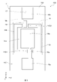
- FIG. 1 is a cross-sectional view schematically showing the configuration of a crystal oscillator in one embodiment.
- FIG. 2 is a cross-sectional view schematically showing the configuration of the crystal oscillator in one embodiment.
- FIG. 3 is a plan view schematically showing the configuration of the crystal vibration element in one embodiment.
- FIG. 4 is a cross-sectional view schematically showing the configuration of the crystal oscillator in one embodiment.
- FIG. 5 is a plan view schematically showing the configuration of the crystal vibration element in the first modification of the embodiment.
- FIG. 6 is a plan view schematically showing the configuration of the crystal vibration element in the second modification of the embodiment.
- FIG. 7 is a plan view schematically showing the configuration of the crystal vibration element in the third modification of the embodiment.
- FIG. 1 is a cross-sectional view schematically showing the configuration of a crystal oscillator in one embodiment.
- FIG. 2 is a cross-sectional view schematically showing the configuration of the crystal oscillator in one embodiment.
- FIG. 3 is
- FIG. 8 is a plan view schematically showing the configuration of the crystal vibration element in the fourth modification of the embodiment.
- FIG. 9 is a plan view schematically showing the configuration of the crystal vibration element in the fifth modification of the embodiment.
- FIG. 10 is a plan view schematically showing the configuration of the crystal vibration element in the sixth modification of the embodiment.
- FIG. 11 is a plan view schematically showing the configuration of the crystal vibration element in the seventh modification of the embodiment.
- FIG. 12 is a flowchart showing a method for manufacturing a crystal oscillator according to an embodiment.
- Each drawing should be provided with a Cartesian coordinate system consisting of X-axis, Y'axis and Z'axis for convenience to clarify the mutual relationship of each drawing and to help understand the positional relationship of each member.
- the X-axis, Y'axis and Z'axis correspond to each other in the drawings.
- the X-axis, Y'axis, and Z'axis correspond to the crystallographic axes of the crystal piece 11 described later, respectively.
- the X-axis corresponds to the electric axis (polar axis) of the crystal
- the Y-axis corresponds to the mechanical axis of the crystal
- the Z-axis corresponds to the optical axis of the crystal.
- the Y'axis and the Z'axis are axes obtained by rotating the Y axis and the Z axis around the X axis in the direction of the Y axis to the Z axis by 35 degrees 15 minutes ⁇ 1 minute 30 seconds, respectively.
- the direction parallel to the X-axis is referred to as "X-axis direction”
- the direction parallel to the Y'axis is referred to as “Y'axis direction”
- the direction parallel to the Z'axis is referred to as "Z'axis direction”.
- the direction of the tip of the arrow on the X-axis, Y'axis and Z'axis is called “positive” or “+ (plus)”
- the direction opposite to the arrow is called “negative” or "-(minus)”.
- the + Y'axis direction will be described as an upward direction
- the ⁇ Y'axis direction will be described as a downward direction
- the vertical orientations of the crystal vibrating element 10, the crystal oscillator 1, and the crystal oscillator 100 are limited. is not.
- the plane specified by the X-axis and the Z'axis is referred to as the Z'X plane, and the same applies to the plane specified by the other axes.
- FIG. 1 is a cross-sectional view schematically showing the configuration of the crystal oscillator 100 in one embodiment.
- a piezoelectric oscillator a crystal oscillator (XO: Crystal Oscillator) equipped with a crystal oscillator (Quartz Crystal Oscillator Unit) will be described as an example.
- a crystal oscillator (Quartz Crystal Resonator Unit) provided with a crystal vibration element (Quartz Crystal Resonator) will be described as an example.
- a crystal vibration element a crystal vibration element provided with a crystal piece (Quartz Crystal Blank) will be described as an example.
- Quartz piece is a kind of piezoelectric body (piezoelectric piece) that vibrates according to applied voltage.
- the piezoelectric oscillator is not limited to the crystal oscillator, and may use another piezoelectric material such as ceramic.
- the piezoelectric vibrator is not limited to the crystal oscillator, and other piezoelectric materials such as ceramics may be used.
- the piezoelectric vibration element is not limited to the crystal vibration element, and other piezoelectric materials such as ceramics may be used.
- the crystal oscillator 100 includes a crystal oscillator 1, a mounting substrate 130, a lid member 140, and an electronic component 156.
- the mounting board 130 and the lid member 140 of the present embodiment correspond to an example of the “cover body”.
- the crystal oscillator 1 and the electronic component 156 are housed in a space formed between the mounting substrate 130 and the lid member 140.
- the space formed by the mounting substrate 130 and the lid member 140 is, for example, airtightly sealed. This space may be hermetically sealed in a vacuum state, or may be hermetically sealed in a state filled with a gas such as an inert gas.
- the mounting board 130 is a flat plate-shaped circuit board.
- the mounting substrate 130 includes, for example, a glass epoxy plate and a wiring layer patterned on the glass epoxy plate.
- the crystal oscillator 1 is provided on one surface (upper surface in FIG. 1) of the mounting substrate 130. More specifically, the crystal oscillator 1 is electrically connected to the wiring layer of the mounting substrate 130 by the bonding wire 166. Further, the crystal oscillator 1 and the wiring layer of the mounting substrate 130 are joined by the solder 153. As a result, the crystal oscillator 1 is sealed in the space formed between the mounting substrate 130 and the lid member 140.
- the lid member 140 includes a bottomed opening with one side (lower side in FIG. 1) open.
- the lid member 140 includes a flat plate-shaped top wall portion, a side wall portion extending from the outer edge of the top wall portion toward the mounting substrate 130, and a flange portion extending outward from the tip of the side wall portion. ..
- the flange portion is joined to the mounting substrate 130 on one surface (upper surface in FIG. 1).
- the crystal oscillator 1 joined to the mounting substrate 130 is housed inside the lid member 140.
- the lid member 140 is made of a metal material, and is formed, for example, by drawing a metal plate.
- the electronic component 156 is provided on one surface (upper surface in FIG. 1) of the mounting board 130. More specifically, the wiring layer of the mounting board 130 and the electronic component 156 are joined by the solder 153. As a result, the electronic component 156 is mounted on the mounting board 130.
- the electronic component 156 is electrically connected to the crystal oscillator 1 through the wiring layer of the mounting board 130.
- the electronic component 156 includes, for example, a capacitor, an IC chip, and the like.
- the electronic component 156 is, for example, a part of an oscillation circuit that oscillates the crystal oscillator 1, a part of a temperature compensation circuit that compensates for the temperature characteristics of the crystal oscillator 1, and the like.
- the crystal oscillator 100 may be referred to as a temperature compensating crystal oscillator (TCXO: Temperature Compensated Crystal Oscillator).
- FIG. 2 is a cross-sectional view schematically showing the configuration of the crystal oscillator 1 in one embodiment.
- FIG. 3 is a plan view schematically showing the configuration of the crystal vibration element 10 in one embodiment.
- FIG. 4 is a cross-sectional view schematically showing the configuration of the crystal oscillator 1 in one embodiment. Note that FIG. 2 shows a cross section parallel to the XY'plane along the line II-II shown in FIG.
- FIG. 4 shows a cross section parallel to the XY'plane along the IV-IV line shown in FIG.
- the crystal oscillator 1 includes a crystal vibrating element 10, an upper lid 20, a joint portion 30, an insulating layer 40, and a support substrate 50.
- the upper lid 20 of the present embodiment corresponds to an example of the "cover member”.
- the crystal vibration element 10 is an element that vibrates a crystal by a piezoelectric effect and converts electrical energy and mechanical energy.
- the crystal vibrating element 10 includes an AT-cut type crystal piece 11.
- the AT-cut type crystal piece 11 has the Y-axis and the Z-axis in the direction from the Y-axis to the Z-axis around the X-axis among the X-axis, the Y-axis, and the Z-axis which are the crystal axes of the artificial crystal (Synthetic Quartz Crystal).
- the rotation angles of the Y'axis and the Z'axis in the AT-cut type crystal piece 11 may be tilted in the range of -5 degrees or more and +15 degrees or less from 35 degrees 15 minutes. Further, as the cut angle of the crystal piece 11, a different cut other than the AT cut, for example, a BT cut, a GT cut, an SC cut, or the like may be applied.
- a crystal vibration element using an AT-cut crystal piece has high frequency stability in a wide temperature range.
- the AT-cut crystal vibrating element is excellent in aging characteristics and can be manufactured at low cost.
- the AT-cut crystal vibration element uses a thickness slip vibration mode (Thickness Shear Vibration Mode) as the main vibration.
- the crystal vibration element 10 includes a set of excitation electrodes. An alternating electric field is applied between this set of excitation electrodes. As a result, the vibrating portion 11A of the crystal piece 11 vibrates at a predetermined oscillation frequency in the thickness slip vibration mode, and the resonance characteristic associated with the vibration is obtained.
- the main vibration of the crystal vibrating element 10 is in the thickness slip vibration mode, for example, by using the AT-cut crystal piece 11, it is easy to make the crystal oscillator 1 that performs the thickness slip vibration at the vibration frequency in the MHz band. Can be realized.
- the crystal piece 11 has a first main surface 12a and a second main surface 12b that are XZ'planes and face each other.
- the crystal piece 11 has a flat plate shape. Therefore, the first main surface 12a and the second main surface 12b of the crystal piece 11 are flat surfaces, respectively.
- the crystal piece 11 is not limited to a flat plate shape, and may have a convex or concave shape at the center, for example.
- the AT-cut type crystal piece 11 is parallel to the long side direction in which the long side parallel to the X-axis direction extends, the short side direction in which the short side parallel to the Z'axis direction extends, and the Y'axis direction. Has a thickness direction in which the thickness is extended.
- the crystal piece 11 has a rectangular shape when the first main surface 12a of the crystal piece 11 is viewed in a plan view (hereinafter, simply referred to as “planar view”).
- the length of the crystal piece 11 in the direction parallel to the X-axis direction is, for example, about 180 ⁇ m
- the length of the crystal piece 11 in the direction parallel to the Z'axis direction is, for example, about 180 ⁇ m.
- the thickness of the crystal piece 11 is, for example, within the range of 0.5 ⁇ m or more and 3 ⁇ m or less, for example, about 1 ⁇ m.
- the crystal piece 11 may be thinned to a predetermined thickness by, for example, being bonded to the support substrate 50 via an insulating layer 40 described later and then polished in a state of having a larger thickness.
- the planar shape of the crystal piece 11 is not limited to a rectangular shape.
- the planar shape of the crystal piece 11 may be a polygonal shape, a circular shape, an elliptical shape, or a combination thereof.
- the crystal piece 11 includes a vibrating portion 11A, an opening portion 11B, and a holding portion 11C.
- the vibrating portion 11A of the crystal piece 11 vibrates at a predetermined oscillation frequency with the thickness slip vibration mode as the main vibration.
- the vibrating portion 11A has a length of, for example, about 80 ⁇ m in a direction parallel to the X-axis direction, and a length of, for example, about 80 ⁇ m in a direction parallel to the Z'axis direction.
- the crystal vibration element 10 includes a first excitation electrode 14a and a second excitation electrode 14b constituting a set of excitation electrodes.
- the first excitation electrode 14a and the second excitation electrode 14b are arranged in the vibrating portion 11A of the crystal piece 11. More specifically, the first excitation electrode 14a is provided on the first main surface 12a of the vibrating portion 11A, and the second excitation electrode 14b is provided on the second main surface 12b of the vibrating portion 11A.
- the first excitation electrode 14a and the second excitation electrode 14b are provided so as to face each other with the crystal piece 11 interposed therebetween.
- the first excitation electrode 14a and the second excitation electrode 14b each have a rectangular shape when the first main surface 12a is viewed in a plane, and are arranged so that substantially the entire surface overlaps on the XZ'plane.
- the first excitation electrode 14a and the second excitation electrode 14b each have a length of about 50 ⁇ m in the direction parallel to the X-axis direction and, for example, about 50 ⁇ m in the direction parallel to the Z'axis direction.
- the first excitation electrode 14a and the second excitation electrode 14b are not limited to a rectangular shape, respectively, and may be a polygonal shape, a circular shape, an elliptical shape, or a combination thereof.
- the opening 11B of the crystal piece 11 is an opening formed so as to surround the vibrating portion 11A when the first main surface 12a is viewed in a plan view.
- the opening penetrates in the thickness direction of the crystal piece 11 parallel to the Z'axis direction and leads to the cavity portion 41 described later.
- the opening 11B is formed so that the vibrating portion 11A and the holding portion 11C are separated from each other by, for example, about 10 ⁇ m.
- the holding portion 11C of the crystal piece 11 holds one end portion (lower end portion in FIG. 2) of the vibrating portion 11A.
- the holding portion 11C is connected to the side of the vibrating portion 11A on the negative direction side of the X-axis.
- the crystal vibration element 10 further includes a first extraction electrode 15a, a second extraction electrode 15b, a first connection electrode 16a, a second connection electrode 16b, and a via electrode 17.
- the first extraction electrode 15a, the second extraction electrode 15b, the first connection electrode 16a, the second connection electrode 16b, and the via electrode 17 are provided on the holding portion 11C of the crystal piece 11.
- the first extraction electrode 15a is provided on the first main surface 12a of the crystal piece 11, and is electrically connected to the first excitation electrode 14a.
- the second extraction electrode 15b is provided on the second main surface 12b of the crystal piece 11, and is electrically connected to the second excitation electrode 14b.
- the second extraction electrode 15b and the second connection electrode 16b are electrically connected by a via electrode 17 penetrating in the thickness direction of the crystal piece 11.
- the first connection electrode 16a is electrically connected to the first excitation electrode 14a via the first extraction electrode 15a. Further, the second connection electrode 16b is electrically connected to the second excitation electrode 14b via the second extraction electrode 15b and the via electrode 17.
- the first connection electrode 16a and the second connection electrode 16b are terminals for electrically connecting to an external electrode (not shown) provided on the upper lid 20, respectively.
- the first connection electrode 16a and the second connection electrode 16b are provided on the first main surface 12a of the crystal piece 11, respectively.
- Each of the first connection electrode 16a and the second connection electrode 16b has a length of about 15 ⁇ m in the direction parallel to the X-axis direction and, for example, about 20 ⁇ m in the direction parallel to the Z'axis direction.
- the via electrode 17 is provided so as to penetrate from the first main surface 12a to the second main surface 12b of the crystal piece 11.
- the material of the via electrode 17 is, for example, aluminum (Al), and the thickness of the via electrode 17 is, for example, 1.0 ⁇ m.
- the material of the via electrode 17 may be, for example, copper (Cu).
- the thickness of the via electrode 17 is, for example, in the range of 0.5 ⁇ m or more and 3.0 ⁇ m or less.
- the first excitation electrode 14a is provided on the first main surface 12a
- the second excitation electrode 14b is provided on the second main surface 12b
- the second extraction electrode 15b is electrically connected to the second excitation electrode 14b.
- an alternating electric field is applied to the first excitation electrode 14a and the second excitation electrode 14b via the first extraction electrode 15a, the second extraction electrode 15b, the first connection electrode 16a, the second connection electrode 16b, and the via electrode 17.
- the materials of the first excitation electrode 14a, the second excitation electrode 14b, the first extraction electrode 15a, the second extraction electrode 15b, and the first connection electrode 16a and the second connection electrode 16b are, for example, aluminum (Al) and molybdenum (Mo). ) Or gold (Au).
- the thickness of the first excitation electrode 14a and the second excitation electrode 14b is, for example, within the range of 0.05 ⁇ m or more and 0.2 ⁇ m or less, respectively.
- each of the above-mentioned electrodes may be, for example, a laminated body composed of a titanium (Ti) layer provided on the crystal piece 11 side and a gold (Au) layer provided on the surface side.
- the thickness of the titanium layer is, for example, about 0.005 ⁇ m
- the thickness of the gold layer is, for example, about 0.05 ⁇ m.
- the upper lid 20 is a flat plate-shaped member.
- the dimensions of the upper lid 20 in a plan view are the same as or substantially the same as the dimensions of the crystal vibrating element 10 (crystal piece 11).
- the length of the upper lid 20 in the direction parallel to the X-axis direction is, for example, about 180 ⁇ m, and the length of the upper lid 20 in the direction parallel to the Z'axis direction is, for example, about 180 ⁇ m.
- the thickness of the upper lid 20 is, for example, in the range of 100 ⁇ m or more and 200 ⁇ m or less.
- the material of the upper lid 20 is, for example, quartz. This makes it possible to reduce the stress caused by the difference in the coefficient of thermal expansion between the joint portion 30 and the crystal vibrating element 10.
- the upper lid 20 is not limited to the case of a quartz plate, and may be, for example, a ceramic plate or a glass plate.
- the upper lid 20 may have conductivity.
- the upper lid 20 is composed of 42 alloy, which is an alloy containing iron (Fe) and nickel (Ni), or Kovar, which is an alloy containing iron (Fe), nickel (Ni), and cobalt (Co). To.
- the joint portion 30 joins the crystal vibration element 10 and the upper lid 20.
- a space is formed by the bonded upper lid 20 and the crystal vibrating element 10.
- the space forms a part of the vibration space of the vibration unit 11A.
- the joint portion 30 is provided over the entire circumference of each of the upper lid 20 and the crystal vibrating element 10.
- the joint portion 30 is provided on the lower surface of the upper lid 20 and the first main surface 12a of the crystal piece 11.
- the joint portion 30 has a frame shape when the first main surface 12a is viewed in a plan view.
- the width of the frame that is, the difference between the outer circumference and the inner circumference is, for example, about 20 ⁇ m.
- the joint portion 30 has electrical insulating property (non-conductive).
- the joint portion 30 is, for example, a glass adhesive which is made of inorganic glass and solidifies by heat treatment to exhibit an adhesive action.
- the inorganic glass is, for example, a low melting point glass such as lead boric acid type and tin phosphoric acid type.
- the material of the joint portion 30 is a low melting point glass adhesive
- it may contain lead-free vanadium (V) -based glass that melts at a temperature of 300 ° C. or higher and 410 ° C. or lower.
- Vanadium-based glass exhibits an adhesive action by adding a binder and a solvent in the form of a paste, melting the glass, and solidifying the glass.
- the vanadium-based glass may contain other metals such as silver (Ag).
- the material of the joint portion 30 may be, for example, a resin adhesive.
- the resin adhesive may contain a thermosetting resin or a photocurable resin, and for example, an epoxy-based adhesive containing an epoxy resin as a main component can be used.
- an epoxy resin for example, bifunctional epoxy resins such as bisphenol A type epoxy resin and bisphenol F type epoxy resin, novolak type epoxy resins such as phenol novolac type epoxy resin and cresol novolac type epoxy resin can be used.
- generally known ones such as a polyfunctional epoxy resin, a glycidylamine type epoxy resin, a heterocyclic-containing epoxy resin or an alicyclic epoxy resin can also be applied.
- the insulating layer 40 includes a cavity 41 formed in a portion corresponding to the vibrating portion 11A of the crystal vibrating element 10.
- the hollow portion 41 has a concave shape and forms a space between the hollow portion 41 and the second excitation electrode 14b provided on the second main surface 12b of the crystal piece 11.
- the insulating layer 40 joins the crystal vibration element 10 and the support substrate 50. More specifically, the insulating layer 40 is formed on the lower surface of the crystal vibrating element 10, and joins the upper surface of the support substrate 50 and the second main surface 12b of the crystal piece 11.
- the insulating layer 40 joins the crystal vibrating element 10 and the support substrate 50, so that the crystal vibrating element 10 can be sealed between the upper lid 20 and the support substrate 50, for example.
- the material of the insulating layer 40 is, for example, a silicon oxide film (silicon dioxide (SiO 2 )). This makes it possible to reduce the stress caused by the difference in the coefficient of thermal expansion from the crystal vibrating element 10 and the stress caused by the difference in the coefficient of thermal expansion from the support substrate 50.
- the thickness of the insulating layer 40 is preferably 0.5 ⁇ m or more, and is, for example, in the range of 1 ⁇ m or more and 1.5 ⁇ m or less.
- the thickness (depth) of the cavity 41 parallel to the Y'axis direction is, for example, in the range of 0.2 ⁇ m or more and 0.5 ⁇ m or less.
- the thickness of the joint portion 30 described above is set to be larger than the thickness of the insulating layer 40. More specifically, the thickness of the joint portion 30 is, for example, in the range of 2 ⁇ m or more and 90 ⁇ m or less. As a result, the thickness (depth) of the space formed between the upper lid 20 and the crystal vibrating element 10 by the joint portion 30 parallel to the Y'axis direction is increased by the hollow portion 41 between the insulating layer 40 and the crystal vibrating element 10. It can be larger than the thickness (depth) parallel to the Y'axis direction of the space formed between and. Therefore, it is possible to alleviate the influence of the stress caused by the difference in the coefficient of thermal expansion between the joint portion 30 and the crystal vibrating element 10 on the vibrating portion 11A.
- the material of the insulating layer 40 is not limited to the silicon oxide film, and may be a silicon nitride film (silicon nitride (Si 3N 4 ) ) or various adhesives.
- the support substrate 50 is configured to support the crystal vibration element 10 and the insulating layer 40. As a result, the vibrating portion 11A of the crystal vibrating element 10 can be vibratedly supported.
- the support substrate 50 is, for example, a flat plate-shaped substrate.
- the dimensions of the support substrate 50 in a plan view are the same as or substantially the same as the dimensions of the crystal vibrating element 10 (crystal piece 11).
- the length of the support substrate 50 in the direction parallel to the X-axis direction is, for example, about 180 ⁇ m, and the length of the support substrate 50 in the direction parallel to the Z'axis direction is, for example, about 180 ⁇ m.
- the thickness of the support substrate 50 is, for example, in the range of 50 ⁇ m or more and 500 ⁇ m or less.
- the material of the support substrate 50 is, for example, quartz. This makes it possible to reduce the stress caused by the difference in the coefficient of thermal expansion between the crystal vibrating element 10 and the insulating layer 40.
- the support substrate 50 is not limited to a crystal substrate, and may be, for example, a silicon substrate.
- the thickness of the first extraction electrode 15a is set to be larger than the thickness of the second extraction electrode 15b. More specifically, the thickness of the first extraction electrode 15a is, for example, about 1 ⁇ m, and the thickness of the second extraction electrode 15b is, for example, in the range of 0.5 or more and less than 1 ⁇ m.
- the stress generated in the first extraction electrode 15a and the second extraction electrode 15b is proportional to the respective thicknesses. Therefore, the stress of the first extraction electrode 15a is larger than the stress of the second extraction electrode 15b.
- the end portion (upper end portion in FIG. 3) of the first extraction electrode 15a extends beyond the end portion of the cavity portion 41 existing below the vibrating portion 11A, and the first excitation electrode 14a Is electrically connected to.
- the end portion of the first extraction electrode 15a is arranged on one side (X-axis positive direction side in FIG. 3) including the vibration portion 11A with respect to the end portion of the cavity portion 41 in a plan view.
- the stress of the first extraction electrode 15a which is larger than the stress of the second extraction electrode 15b, can be applied in the direction of pulling up the vibrating portion 11A. Therefore, the vibrating portion 11A is pulled toward the first extraction electrode 15a, and sticking that the vibrating portion 11A adheres to the insulating layer 40 can be suppressed.
- the end portion (upper end portion in FIG. 3) of the second extraction electrode 15b does not extend to the end portion of the cavity portion 51 existing below the vibrating portion 11A, and the second portion is in front of the end portion of the cavity portion 41. It is electrically connected to the excitation electrode 14b.
- the end portion of the second extraction electrode 15b is arranged on the opposite side (X-axis negative direction side in FIG. 3) with respect to the end portion of the cavity portion 41 in a plan view.
- the opening 11B is arranged on one side including the vibrating portion 11A (inside the cavity 41 in FIG. 3) with respect to the end of the cavity 41 in a plan view.
- the opening 11B by arranging the opening 11B inside the vibrating portion 11A, the influence of the stress caused by the difference in the coefficient of thermal expansion between the insulating layer 40 and the crystal vibrating element 10 on the vibrating portion 11A can be alleviated. can. Therefore, the characteristics such as the vibration frequency and the Q value of the crystal vibration element 10 can be stabilized.
- the joint portion 30 is arranged on the opposite side (outside of the cavity portion 41 in FIG. 3) with respect to the end portion of the cavity portion 41 in a plan view.
- the joint portion 30 is arranged outside the vibrating portion 11A, it is possible to alleviate the influence of the stress caused by the difference in the coefficient of thermal expansion between the joint portion 30 and the crystal vibrating element 10 on the vibrating portion 11A. can. Therefore, the characteristics such as the vibration frequency and the Q value of the crystal vibration element 10 can be stabilized.
- FIG. 5 is a plan view schematically showing the configuration of the crystal vibration element 10A in the first modification of the first embodiment.
- FIG. 6 is a plan view schematically showing the configuration of the crystal vibration element 10B in the second modification of the embodiment.
- FIG. 7 is a plan view schematically showing the configuration of the crystal vibration element 10C in the third modification of the embodiment.
- FIG. 8 is a plan view schematically showing the configuration of the crystal vibration element 10D in the fourth modification of the embodiment.
- FIG. 9 is a plan view schematically showing the configuration of the crystal vibration element 10E in the fifth modification of the embodiment.
- FIG. 10 is a plan view schematically showing the configuration of the crystal vibration element 10F in the sixth modification of the embodiment.
- FIG. 11 is a plan view schematically showing the configuration of the crystal vibration element 10G in the seventh modification of the embodiment.
- the crystal vibration element 10A further includes a conductive conductor 18.
- the conductor 18 is provided on the first main surface 12a, and is arranged between the first excitation electrode 14a and the second connection electrode 16b in a plan view. In other words, the conductor 18 is not electrically connected to the first excitation electrode 14a and the second connection electrode 16b.
- the thickness of the conductor 18 is set to be larger than the thickness of the second extraction electrode 15b. More specifically, the thickness of the conductor 18 is, for example, about 1 ⁇ m. Further, the end portion (upper end portion in FIG. 5) of the conductor 18 is arranged on one side (X-axis positive direction side in FIG. 5) including the vibration portion 11A with respect to the end portion of the cavity portion 41. As a result, the stress of the conductor 18, which is larger than the stress of the second extraction electrode 15b, can be applied in the direction of further pulling up the vibrating portion 11A.
- the crystal piece 11 of the crystal vibration element 10B includes a connecting portion 11D and a slit 11E.
- the connecting portion 11D connects the vibrating portion 11A and the holding portion 11C. More specifically, the connecting portion 11D connects the vibrating portion 11A and the holding portion 11C on one side (lower side in FIG. 6) with respect to the vibrating portion 11A.
- the slit 11E is formed in the connecting portion 11D. That is, the slit 11E is a hole formed between the vibrating portion 11A and the holding portion 11C that holds one end (lower end in FIG. 6) of the vibrating portion 11A. The hole penetrates in the thickness direction of the crystal piece 11 and leads to the cavity 41. As a result, vibration leakage from the vibrating portion 11A to the holding portion 11C can be reduced.
- the crystal piece 11 includes the connecting portion 11D and the slit 11E, similarly to the crystal vibrating element 10B shown in FIG. Further, the crystal vibrating element 10C may include the conductor 18 in the same manner as the crystal vibrating element 10A shown in FIG.
- FIGS. 3 and 5 to 7 show an example of a so-called cantilever structure in which the holding portion 11C holds the vibrating portion 11A at one place, but the present invention is not limited to this.
- the crystal piece 11 may include two connecting portions 11D1 and 11D2.
- the connecting portion 11D1 connects the vibrating portion 11A and the holding portion 11C on one side (lower side in FIG. 8) with respect to the vibrating portion 11A in a plan view.
- the connecting portion 11D2 connects the vibrating portion 11A and the holding portion 11C on the other side (upper side in FIG. 8) with respect to the vibrating portion 11A in a plan view.
- the first extraction electrode 15a is provided on the connecting portion 11D and the holding portion 11C on one side (lower side in FIG. 8) with respect to the vibrating portion 11A on the first main surface 12a.
- the second extraction electrode 15b is provided on the holding portion 11C on the second main surface 12b on the other side (upper side in FIG. 8) with respect to the vibrating portion 11A.
- the first connection electrode 16a is provided on the holding portion 11C on one side (lower side in FIG. 8) with respect to the vibrating portion 11A on the first main surface 12a.
- the second connection electrode 16b and the via electrode 17 are provided on the holding portion 11C on the other side (upper side in FIG. 8) with respect to the vibrating portion 11A on the first main surface 12a.
- the crystal vibrating element 10D may include the conductor 18 in the same manner as the crystal vibrating element 10A shown in FIG.
- the crystal piece 11 of the crystal vibrating element 10E includes two connecting portions 11D1 and 11D2, and the connecting portions 11D1 and 11D2 each have a corner portion and a holding portion 11C of the vibrating portion 11A. It may be connected.
- FIGS. 8 and 9 show an example of a so-called double-sided structure in which the holding portion 11C holds the vibrating portion 11A at two locations, but the present invention is not limited to this.
- the crystal piece 11 may include three connecting portions 11D1, 11D2, 11D3.
- the holding portion 11C holds the vibrating portion 11A at three locations via the connecting portions 11D1, 11D2, and 11D3.
- the crystal piece 11 may include four connecting portions 11D1, 11D2, 11D3, 11D4.
- the holding portion 11C holds the vibrating portion 11A at four locations via the connecting portions 11D1, 11D2, 11D3, and 11D4.
- the crystal vibrating element 10F and the crystal vibrating element 10G may further include one or a plurality of conductors 18.
- FIG. 12 is a flowchart showing a method of manufacturing the crystal oscillator 1 according to the embodiment.
- the crystal oscillator 1 shall include the crystal vibration element 10 shown in FIGS. 2 to 4.
- the crystal vibration element 10 is prepared (S301). Specifically, the crystal piece 11, the first excitation electrode 14a and the second excitation electrode 14b arranged in the vibrating portion 11A of the crystal piece 11, and the second drawer provided on the second main surface 12b of the crystal piece 11. A crystal vibration element 10 including an electrode 15b is prepared. However, the first connection electrode 16a, the second connection electrode 16b, and the first extraction electrode 15a are not yet provided on the first main surface 12a of the crystal piece 11. Further, the holding portion 11C of the crystal piece 11 is not provided with the via electrode 17 penetrating in the thickness direction of the crystal piece 11. Further, the opening 11B is not formed around the vibrating portion 11A.
- the insulating layer 40 is formed on the crystal vibration element 10 prepared in step S301 (S302). Specifically, the insulating layer 40 is formed on substantially the entire surface of the second main surface 12b of the quartz piece 11 including the second connecting electrode 16b and the second extraction electrode 15b.
- step S301 the crystal vibration element 10 prepared in step S301 and the insulating layer 40 formed in step S302 are joined to the support substrate 50 (S303).
- the first connection electrode 16a, the second connection electrode 16b, and the via electrode 17 are provided (S304).
- the first connection electrode 16a, the second connection electrode 16b, and the via electrode 17 are each provided in the region corresponding to the holding portion 11C on the first main surface 12a of the crystal piece 11.
- the first connection electrode 16a and the second connection electrode 16b are patterned (formed) by, for example, thin-film deposition and lift-off methods, sputtering, etching, or the like, respectively.
- the via electrode 17 When forming the via electrode 17, first, a hole penetrating the crystal piece 11 is formed at a predetermined position in the holding portion 11C of the crystal piece 11 by wet etching or dry etching. Then, when the hole is filled with the conductive material, the via electrode 17 is formed.
- the opening 11B is formed in the crystal vibration element 10 provided with the first connection electrode 16a, the second connection electrode 16b, and the via electrode 17 (S305).
- the opening 11B is formed so as to surround at least a part around the vibrating portion 11A provided with the first excitation electrode 14a and the second excitation electrode 14b in a plan view.
- the opening 11B is formed by forming an opening penetrating the crystal piece 11 around the vibrating portion 11A by wet etching or dry etching.
- the first extraction electrode 15a is provided (S306).
- the first extraction electrode 15a is provided extending from the holding portion 11C to the vibrating portion 11A on the first main surface 12a of the crystal piece 11.
- the first extraction electrode 15a is patterned (formed) by, for example, thin-film deposition and lift-off methods, sputtering, etching, or the like, respectively.
- a part of the insulating layer 40 is removed to form the cavity 41 (S307).
- the removal of the insulating layer 40 is performed through the opening 11B formed in step S305. Specifically, the insulating layer 40 exposed by the opening 11B of the crystal piece 11 is etched or the like to remove a part of the insulating layer 40. As a result, a concave cavity 41 is formed in the insulating layer 40.
- the crystal vibrating element 10 in which the cavity 41 is formed in the insulating layer 40 in step S307 is joined to the upper lid 20 (S308).
- the joining of the crystal vibrating element 10 and the upper lid 20 is performed via the joining portion 30.
- the joint portion 30 is formed on at least one of the outer peripheral portion of the first main surface 12a of the crystal piece 11 and the outer peripheral portion of the surface of the upper lid 20 facing the crystal vibrating element 10.
- the crystal vibrating element 10 and the upper lid 20 are joined by aligning the positions of the crystal vibrating element 10 and the upper lid 20 and performing heat treatment and / or pressure treatment.
- the thickness of the first extraction electrode is larger than the thickness of the second extraction electrode.
- the stress generated in the first extraction electrode and the second extraction electrode is proportional to the thickness of each. Therefore, the stress of the first extraction electrode is larger than the stress of the second extraction electrode.
- the end portion of the first extraction electrode is arranged on one side including the vibrating portion with respect to the end portion of the cavity portion in a plan view. As a result, the stress of the first extraction electrode, which is larger than the stress of the second extraction electrode, can be applied in the direction of pulling up the vibrating portion. Therefore, the vibrating portion is pulled toward the first extraction electrode side, and sticking that the vibrating portion adheres to the insulating layer can be suppressed.
- the end portion of the second extraction electrode is arranged on the opposite side of the end portion of the cavity portion in a plan view.
- the thickness of the conductor is larger than the thickness of the second extraction electrode, and the end portion of the conductor 18 is arranged on one side including the vibrating portion with respect to the end portion of the cavity portion.
- the stress of the conductor which is larger than the stress of the second extraction electrode, can be applied in the direction of further pulling up the vibrating portion.
- the opening is arranged on one side including the vibrating portion with respect to the end portion of the cavity portion in a plan view.
- the crystal vibrating element further includes a slit formed between the vibrating portion and the holding portion that holds one end of the vibrating portion. This makes it possible to reduce vibration leakage from the vibrating portion to the holding portion.
- a support substrate for supporting the crystal vibration element and the insulating layer is further provided. As a result, the vibrating portion of the crystal vibrating element can be vibratedly supported.
- the insulating layer joins the crystal vibrating element and the support substrate, and the material of the insulating layer is a silicon oxide film (silicon dioxide (SiO 2 )). This makes it possible to reduce the stress caused by the difference in the coefficient of thermal expansion from the crystal vibrating element and the stress caused by the difference in the coefficient of thermal expansion from the support substrate.
- the material of the support substrate is quartz. This makes it possible to reduce the stress caused by the difference in the coefficient of thermal expansion between the crystal vibrating element and the insulating layer.
- the main vibration of the crystal vibration element is the thickness slip vibration mode.
- the material of the piezoelectric piece is quartz. This makes it possible to easily realize a crystal oscillator that can obtain, for example, a frequency temperature characteristic on the order of ppm.
- the upper lid is further provided with a joint portion for joining the crystal vibrating element and the upper lid.
- the crystal vibration element 10 can be sealed between the upper lid 20 and the support substrate 50.
- the joint portion is arranged on the other side of the end portion of the cavity portion in a plan view.
- the thickness of the joint portion is larger than the thickness of the insulating layer.
- a thickness (depth) parallel to the Y'axis direction of the space formed between the upper lid and the crystal vibrating element by the joint portion is formed between the insulating layer and the crystal vibrating element by the cavity portion. It can be larger than the thickness (depth) parallel to the Y'axis direction of the space. Therefore, it is possible to alleviate the influence of the stress caused by the difference in the coefficient of thermal expansion between the joint portion and the crystal vibrating element on the vibrating portion.
- the material of the upper lid is, for example, quartz. This makes it possible to reduce the stress caused by the difference in the coefficient of thermal expansion between the joint and the crystal vibrating element.
- a crystal oscillator according to an embodiment includes the above-mentioned crystal oscillator and a lid member. This makes it possible to easily realize a crystal oscillator that suppresses sticking in which the vibrating portion adheres to the insulating layer.
- the thickness of the first extraction electrode is larger than the thickness of the second extraction electrode.
- the stress generated in the first extraction electrode and the second extraction electrode is proportional to the thickness of each. Therefore, the stress of the first extraction electrode is larger than the stress of the second extraction electrode.
- the end portion of the first extraction electrode is arranged on one side including the vibrating portion with respect to the end portion of the cavity portion in a plan view. As a result, the stress of the first extraction electrode, which is larger than the stress of the second extraction electrode, can be applied in the direction of pulling up the vibrating portion. Therefore, the vibrating portion is pulled toward the first extraction electrode side, and sticking that the vibrating portion adheres to the insulating layer can be suppressed.
Abstract
Description
各図面には、各図面の相互の関係を明確にし、各部材の位置関係を理解する助けとするために、便宜的にX軸、Y’軸及びZ’軸からなる直交座標系を付すことがある。X軸、Y’軸及びZ’軸は各図面において互いに対応している。X軸、Y’軸及びZ’軸は、それぞれ、後述する水晶片11の結晶軸(Crystallographic Axes)に対応している。X軸は水晶の電気軸(極性軸)、Y軸は水晶の機械軸、Z軸は水晶の光学軸に、それぞれ相当する。Y’軸及びZ’軸は、それぞれ、Y軸及びZ軸をX軸の周りにY軸からZ軸の方向に35度15分±1分30秒回転させた軸である。 <Embodiment>
Each drawing should be provided with a Cartesian coordinate system consisting of X-axis, Y'axis and Z'axis for convenience to clarify the mutual relationship of each drawing and to help understand the positional relationship of each member. There is. The X-axis, Y'axis and Z'axis correspond to each other in the drawings. The X-axis, Y'axis, and Z'axis correspond to the crystallographic axes of the
図5は、一実施形態の第1変形例における水晶振動素子10Aの構成を概略的に示す平面図である。図6は、一実施形態の第2変形例における水晶振動素子10Bの構成を概略的に示す平面図である。図7は、一実施形態の第3変形例における水晶振動素子10Cの構成を概略的に示す平面図である。図8は、一実施形態の第4変形例における水晶振動素子10Dの構成を概略的に示す平面図である。図9は、一実施形態の第5変形例における水晶振動素子10Eの構成を概略的に示す平面図である。図10は、一実施形態の第6変形例における水晶振動素子10Fの構成を概略的に示す平面図である。図11は、一実施形態の第7変形例における水晶振動素子10Gの構成を概略的に示す平面図である。 (Modification example)
FIG. 5 is a plan view schematically showing the configuration of the
1 ... Crystal oscillator, 10,10A, 10B, 10C, 10D, 10E, 10F, 10G ... Crystal vibrating element, 11 ... Crystal piece, 11A ... Vibrating part, 11B ... Opening, 11C ... Holding part, 11D, 11D1, 11D2, 11D3, 11D4 ... Connecting part, 11E ... Slit, 12a ... First main surface, 12b ... Second main surface, 14a ... First excitation electrode, 14b ... Second excitation electrode, 15a ... First extraction electrode, 15b ... 2nd extraction electrode, 16a ... 1st connection electrode, 16b ... 2nd connection electrode, 17 ... Via electrode, 18 ... Conductor, 20 ... Top lid, 30 ... Joint part, 40 ... Insulation layer, 41 ... Cavity part, 50 ... Support substrate, 100 ... crystal oscillator, 130 ... mounting board, 140 ... lid member, 153 ... solder, 156 ... electronic component, 166 ... bonding wire.
Claims (16)
- 圧電片と、前記圧電片の振動部に配置された第1励振電極及び第2励振電極と、前記圧電片の第1主面に設けられ、前記第1励振電極に電気的に接続される第1引出電極と、前記圧電片の第2主面に設けられ、前記第2励振電極に電気的に接続される第2引出電極と、を含む圧電振動素子と、
前記第2励振電極との間に空間を形成する空洞部を含む絶縁層と、を備え、
前記第1引出電極の厚さは、前記第2引出電極の厚さより大きく、
前記第1引出電極の端部は、平面視において、前記空洞部の端部に対して前記振動部を含む一方側に配置される、
圧電振動子。 The piezoelectric piece, the first excitation electrode and the second excitation electrode arranged in the vibrating portion of the piezoelectric piece, and the first main surface of the piezoelectric piece, which is electrically connected to the first excitation electrode. A piezoelectric vibrating element including a lead-out electrode and a second lead-out electrode provided on the second main surface of the piezoelectric piece and electrically connected to the second excitation electrode.
An insulating layer including a cavity forming a space between the second excitation electrode and the second excitation electrode is provided.
The thickness of the first extraction electrode is larger than the thickness of the second extraction electrode.
The end portion of the first extraction electrode is arranged on one side including the vibrating portion with respect to the end portion of the cavity portion in a plan view.
Piezoelectric oscillator. - 前記第2引出電極の端部は、平面視において、前記空洞部の端部に対して他方側に配置される、
請求項1に記載の圧電振動子。 The end portion of the second extraction electrode is arranged on the opposite side of the end portion of the cavity portion in a plan view.
The piezoelectric vibrator according to claim 1. - 前記圧電振動素子は、前記第1主面に設けられ、前記第1励振電極と電気的に未接続の導電体をさらに含み、
前記導電体の厚さは、前記第2引出電極の厚さより大きく、
前記導電体の端部は、平面視において、前記空洞部の端部に対して前記一方側に配置される、
請求項1又は2に記載の圧電振動子。 The piezoelectric vibration element is provided on the first main surface and further includes a conductor that is not electrically connected to the first excitation electrode.
The thickness of the conductor is larger than the thickness of the second extraction electrode.
The end portion of the conductor is arranged on one side of the end portion of the cavity portion in a plan view.
The piezoelectric vibrator according to claim 1 or 2. - 前記圧電振動素子は、前記振動部の周囲に形成され、前記空間に通ずる開口部をさらに含み、
前記開口部は、平面視において、前記空洞部の端部に対して前記一方側に配置される、
請求項1から3のいずれか一項に記載の圧電振動子。 The piezoelectric vibrating element is formed around the vibrating portion and further includes an opening leading to the space.
The opening is arranged on one side of the end of the cavity in a plan view.
The piezoelectric vibrator according to any one of claims 1 to 3. - 前記圧電振動素子は、前記振動部と前記振動部の一端を保持する保持部との間に形成されたスリットをさらに含む、
請求項1から4のいずれか一項に記載の圧電振動子。 The piezoelectric vibrating element further includes a slit formed between the vibrating portion and a holding portion that holds one end of the vibrating portion.
The piezoelectric vibrator according to any one of claims 1 to 4. - 前記圧電振動素子及び前記絶縁層を支持する支持基板をさらに備える、
請求項1から5のいずれか一項に記載の圧電振動子。 A support substrate that supports the piezoelectric vibration element and the insulating layer is further provided.
The piezoelectric vibrator according to any one of claims 1 to 5. - 前記絶縁層は、前記圧電振動素子と前記支持基板とを接合し、
前記絶縁層の材料は、二酸化ケイ素である、
請求項6に記載の圧電振動子。 The insulating layer joins the piezoelectric vibration element and the support substrate.
The material of the insulating layer is silicon dioxide.
The piezoelectric vibrator according to claim 6. - 前記支持基板の材料は、水晶である、
請求項6又は7に記載の圧電振動子。 The material of the support substrate is quartz.
The piezoelectric vibrator according to claim 6 or 7. - 前記圧電振動素子の主振動は、厚みすべり振動モードである、
請求項1から8のいずれか一項に記載の圧電振動子。 The main vibration of the piezoelectric vibration element is the thickness slip vibration mode.
The piezoelectric vibrator according to any one of claims 1 to 8. - 前記圧電片の材料は、水晶である、
請求項1から9のいずれか一項に記載の圧電振動子。 The material of the piezoelectric piece is quartz.
The piezoelectric vibrator according to any one of claims 1 to 9. - 蓋部材と、
前記圧電振動素子と前記蓋部材とを接合する接合部と、をさらに備える、
請求項1から10のいずれか一項に記載の圧電振動子。 With the lid member,
A joint portion for joining the piezoelectric vibration element and the lid member is further provided.
The piezoelectric vibrator according to any one of claims 1 to 10. - 前記接合部は、平面視において、前記空洞部の端部に対して他方側に配置される、
請求項11に記載の圧電振動子。 The joint is arranged on the opposite side of the end of the cavity in a plan view.
The piezoelectric vibrator according to claim 11. - 前記接合部の厚さは、前記絶縁層の厚さより大きい、
請求項11又は12に記載の圧電振動子。 The thickness of the joint is larger than the thickness of the insulating layer.
The piezoelectric vibrator according to claim 11 or 12. - 前記蓋部材の材料は、水晶である、
請求項11から13のいずれか一項に記載の圧電振動子。 The material of the lid member is quartz.
The piezoelectric vibrator according to any one of claims 11 to 13. - 請求項1から14のいずれか一項に記載の圧電振動子と、
蓋体と、を備える、
圧電発振器。 The piezoelectric vibrator according to any one of claims 1 to 14,
With a lid,
Piezoelectric oscillator. - 圧電片と、前記圧電片の振動部に配置された第1励振電極及び第2励振電極と、前記圧電片の第2主面に設けられ、前記第2励振電極に電気的に接続される第2引出電極と、を含む圧電振動素子を用意する工程と、
前記第2励振電極及び前記第2引出電極を覆う絶縁層を形成する工程と、
前記圧電片の第1主面に、前記第1励振電極に電気的に接続される第1引出電極を設ける工程と、
前記絶縁層の一部を除去して空洞部を形成する工程であって、前記空洞部は前記第2励振電極との間に空間を形成する、形成する工程と、を含み、
前記第1引出電極の厚さは、前記第2引出電極の厚さより大きく、
前記第1引出電極の端部は、平面視において、前記空洞部の端部に対して前記振動部を含む一方側に配置される、
圧電振動子製造方法。 The piezoelectric piece, the first excitation electrode and the second excitation electrode arranged in the vibrating portion of the piezoelectric piece, and the second excitation electrode provided on the second main surface of the piezoelectric piece and electrically connected to the second excitation electrode. 2 The process of preparing a piezoelectric vibrating element including a lead-out electrode and
A step of forming an insulating layer covering the second excitation electrode and the second extraction electrode, and
A step of providing a first extraction electrode electrically connected to the first excitation electrode on the first main surface of the piezoelectric piece, and
A step of removing a part of the insulating layer to form a cavity, wherein the cavity includes a step of forming a space between the insulating layer and the second excitation electrode.
The thickness of the first extraction electrode is larger than the thickness of the second extraction electrode.
The end portion of the first extraction electrode is arranged on one side including the vibrating portion with respect to the end portion of the cavity portion in a plan view.
Piezoelectric vibrator manufacturing method.
Priority Applications (3)
| Application Number | Priority Date | Filing Date | Title |
|---|---|---|---|
| CN202180082839.2A CN116671005A (en) | 2020-12-11 | 2021-07-07 | Piezoelectric vibrator, piezoelectric oscillator, and method for manufacturing piezoelectric vibrator |
| JP2022568041A JPWO2022123816A1 (en) | 2020-12-11 | 2021-07-07 | |
| US18/133,347 US20230246625A1 (en) | 2020-12-11 | 2023-04-11 | Piezoelectric vibrator, piezoelectric oscillator, and piezoelectric vibrator manufacturing method |
Applications Claiming Priority (2)
| Application Number | Priority Date | Filing Date | Title |
|---|---|---|---|
| JP2020205988 | 2020-12-11 | ||
| JP2020-205988 | 2020-12-11 |
Related Child Applications (1)
| Application Number | Title | Priority Date | Filing Date |
|---|---|---|---|
| US18/133,347 Continuation US20230246625A1 (en) | 2020-12-11 | 2023-04-11 | Piezoelectric vibrator, piezoelectric oscillator, and piezoelectric vibrator manufacturing method |
Publications (1)
| Publication Number | Publication Date |
|---|---|
| WO2022123816A1 true WO2022123816A1 (en) | 2022-06-16 |
Family
ID=81974363
Family Applications (1)
| Application Number | Title | Priority Date | Filing Date |
|---|---|---|---|
| PCT/JP2021/025550 WO2022123816A1 (en) | 2020-12-11 | 2021-07-07 | Piezoelectric vibrator, piezoelectric oscillator, and method for making piezoelectric vibrator |
Country Status (4)
| Country | Link |
|---|---|
| US (1) | US20230246625A1 (en) |
| JP (1) | JPWO2022123816A1 (en) |
| CN (1) | CN116671005A (en) |
| WO (1) | WO2022123816A1 (en) |
Citations (7)
| Publication number | Priority date | Publication date | Assignee | Title |
|---|---|---|---|---|
| JP2004120494A (en) * | 2002-09-27 | 2004-04-15 | Tdk Corp | Thin film piezo-resonator, filter and duplexer using the same, and method of manufacturing thin film piezo-resonator |
| JP2012175405A (en) * | 2011-02-22 | 2012-09-10 | Seiko Epson Corp | Piezoelectric vibrating element, piezoelectric vibrator, piezoelectric oscillator, and electronic equipment |
| JP2014078905A (en) * | 2012-10-12 | 2014-05-01 | Seiko Epson Corp | Vibrator, electronic apparatus, and manufacturing method of vibrator |
| JP2014107711A (en) * | 2012-11-28 | 2014-06-09 | Seiko Epson Corp | Oscillator and electronic apparatus |
| JP2014239392A (en) * | 2013-06-10 | 2014-12-18 | 太陽誘電株式会社 | Acoustic wave device |
| JP2019193168A (en) * | 2018-04-26 | 2019-10-31 | サムソン エレクトロ−メカニックス カンパニーリミテッド. | Bulk acoustic resonator and manufacturing method thereof |
| JP2020053802A (en) * | 2018-09-26 | 2020-04-02 | 株式会社村田製作所 | Oscillation element and oscillator |
-
2021
- 2021-07-07 JP JP2022568041A patent/JPWO2022123816A1/ja active Pending
- 2021-07-07 WO PCT/JP2021/025550 patent/WO2022123816A1/en active Application Filing
- 2021-07-07 CN CN202180082839.2A patent/CN116671005A/en active Pending
-
2023
- 2023-04-11 US US18/133,347 patent/US20230246625A1/en active Pending
Patent Citations (7)
| Publication number | Priority date | Publication date | Assignee | Title |
|---|---|---|---|---|
| JP2004120494A (en) * | 2002-09-27 | 2004-04-15 | Tdk Corp | Thin film piezo-resonator, filter and duplexer using the same, and method of manufacturing thin film piezo-resonator |
| JP2012175405A (en) * | 2011-02-22 | 2012-09-10 | Seiko Epson Corp | Piezoelectric vibrating element, piezoelectric vibrator, piezoelectric oscillator, and electronic equipment |
| JP2014078905A (en) * | 2012-10-12 | 2014-05-01 | Seiko Epson Corp | Vibrator, electronic apparatus, and manufacturing method of vibrator |
| JP2014107711A (en) * | 2012-11-28 | 2014-06-09 | Seiko Epson Corp | Oscillator and electronic apparatus |
| JP2014239392A (en) * | 2013-06-10 | 2014-12-18 | 太陽誘電株式会社 | Acoustic wave device |
| JP2019193168A (en) * | 2018-04-26 | 2019-10-31 | サムソン エレクトロ−メカニックス カンパニーリミテッド. | Bulk acoustic resonator and manufacturing method thereof |
| JP2020053802A (en) * | 2018-09-26 | 2020-04-02 | 株式会社村田製作所 | Oscillation element and oscillator |
Also Published As
| Publication number | Publication date |
|---|---|
| CN116671005A (en) | 2023-08-29 |
| JPWO2022123816A1 (en) | 2022-06-16 |
| US20230246625A1 (en) | 2023-08-03 |
Similar Documents
| Publication | Publication Date | Title |
|---|---|---|
| JP4221756B2 (en) | Piezoelectric oscillator and manufacturing method thereof | |
| JP6663599B2 (en) | Piezoelectric vibrator and method of manufacturing piezoelectric vibrator | |
| JP4815976B2 (en) | Method for manufacturing crystal vibrating device | |
| JP2004208236A (en) | Piezoelectric device, manufacturing method therefor, portable telephone unit utilizing piezoelectric device and electronic equipment utilizing piezoelectric device | |
| JP5824958B2 (en) | Vibration element, vibrator, electronic device, and electronic apparatus | |
| JP5910092B2 (en) | Piezoelectric vibration element, piezoelectric vibrator, electronic device, and electronic apparatus | |
| JP2012090202A (en) | Piezoelectric device and piezoelectric oscillator | |
| JP2011217301A (en) | Piezoelectric device and method of manufacturing the same | |
| WO2022123816A1 (en) | Piezoelectric vibrator, piezoelectric oscillator, and method for making piezoelectric vibrator | |
| WO2022113408A1 (en) | Piezoelectric vibration element, piezoelectric vibrator, and piezoelectric oscillator | |
| JP2013031133A (en) | Piezoelectric vibration device | |
| JP2018026649A (en) | Oscillation device and manufacturing method thereof | |
| JP2007166435A (en) | Crystal oscillation device | |
| JP2015154371A (en) | crystal device | |
| JP2015050520A (en) | Crystal device | |
| WO2021186790A1 (en) | Crystal vibration element, crystal vibrator, and crystal oscillator | |
| WO2023032342A1 (en) | Piezoelectric oscillator | |
| WO2017022504A1 (en) | Electronic component and method for producing same | |
| WO2022130668A1 (en) | Piezoelectric oscillator | |
| JP6537029B2 (en) | Crystal oscillator and method of manufacturing the same | |
| JP5731870B2 (en) | Electronic component package | |
| JP2016040950A (en) | Vibrating element, vibrator, electronic device, and electronic equipment | |
| JP2015070386A (en) | Crystal device | |
| JP2014165758A (en) | Piezoelectric vibration device, and oscillator | |
| JP2002158557A (en) | Holding structure for piezoelectric vibrating device |
Legal Events
| Date | Code | Title | Description |
|---|---|---|---|
| 121 | Ep: the epo has been informed by wipo that ep was designated in this application |
Ref document number: 21902923 Country of ref document: EP Kind code of ref document: A1 |
|
| ENP | Entry into the national phase |
Ref document number: 2022568041 Country of ref document: JP Kind code of ref document: A |
|
| WWE | Wipo information: entry into national phase |
Ref document number: 202180082839.2 Country of ref document: CN |
|
| NENP | Non-entry into the national phase |
Ref country code: DE |
|
| 122 | Ep: pct application non-entry in european phase |
Ref document number: 21902923 Country of ref document: EP Kind code of ref document: A1 |