WO2022113949A1 - 画像表示装置の製造方法および画像表示装置 - Google Patents
画像表示装置の製造方法および画像表示装置 Download PDFInfo
- Publication number
- WO2022113949A1 WO2022113949A1 PCT/JP2021/042841 JP2021042841W WO2022113949A1 WO 2022113949 A1 WO2022113949 A1 WO 2022113949A1 JP 2021042841 W JP2021042841 W JP 2021042841W WO 2022113949 A1 WO2022113949 A1 WO 2022113949A1
- Authority
- WO
- WIPO (PCT)
- Prior art keywords
- light emitting
- layer
- image display
- insulating film
- display device
- Prior art date
Links
- 238000004519 manufacturing process Methods 0.000 title claims abstract description 101
- 238000000034 method Methods 0.000 title claims abstract description 66
- 239000004065 semiconductor Substances 0.000 claims abstract description 213
- 239000000758 substrate Substances 0.000 claims abstract description 94
- 239000013078 crystal Substances 0.000 claims abstract description 36
- 229910052751 metal Inorganic materials 0.000 claims abstract description 29
- 239000002184 metal Substances 0.000 claims abstract description 29
- 238000012545 processing Methods 0.000 claims abstract description 10
- 238000006243 chemical reaction Methods 0.000 claims description 49
- OKTJSMMVPCPJKN-UHFFFAOYSA-N Carbon Chemical compound [C] OKTJSMMVPCPJKN-UHFFFAOYSA-N 0.000 claims description 36
- 229910021389 graphene Inorganic materials 0.000 claims description 36
- JMASRVWKEDWRBT-UHFFFAOYSA-N Gallium nitride Chemical compound [Ga]#N JMASRVWKEDWRBT-UHFFFAOYSA-N 0.000 claims description 15
- 229910002601 GaN Inorganic materials 0.000 claims description 14
- 238000000137 annealing Methods 0.000 claims description 7
- 150000001875 compounds Chemical class 0.000 claims description 4
- 230000000149 penetrating effect Effects 0.000 claims description 3
- 238000000059 patterning Methods 0.000 claims description 2
- 239000010410 layer Substances 0.000 description 589
- 239000010408 film Substances 0.000 description 247
- 239000011229 interlayer Substances 0.000 description 137
- 238000012986 modification Methods 0.000 description 33
- 230000004048 modification Effects 0.000 description 33
- 239000011347 resin Substances 0.000 description 29
- 229920005989 resin Polymers 0.000 description 29
- 230000008569 process Effects 0.000 description 26
- 239000000463 material Substances 0.000 description 21
- 238000004544 sputter deposition Methods 0.000 description 16
- 230000000694 effects Effects 0.000 description 15
- 238000005530 etching Methods 0.000 description 15
- OAICVXFJPJFONN-UHFFFAOYSA-N Phosphorus Chemical compound [P] OAICVXFJPJFONN-UHFFFAOYSA-N 0.000 description 11
- 239000003990 capacitor Substances 0.000 description 11
- 239000007769 metal material Substances 0.000 description 11
- 239000011521 glass Substances 0.000 description 9
- 238000012546 transfer Methods 0.000 description 9
- 230000015572 biosynthetic process Effects 0.000 description 8
- 238000005229 chemical vapour deposition Methods 0.000 description 8
- 238000010586 diagram Methods 0.000 description 8
- 229910004298 SiO 2 Inorganic materials 0.000 description 7
- 239000004020 conductor Substances 0.000 description 7
- 230000007423 decrease Effects 0.000 description 7
- 238000001020 plasma etching Methods 0.000 description 7
- 150000003377 silicon compounds Chemical class 0.000 description 7
- 229910021417 amorphous silicon Inorganic materials 0.000 description 6
- 239000003086 colorant Substances 0.000 description 6
- 230000006798 recombination Effects 0.000 description 6
- 238000005215 recombination Methods 0.000 description 6
- 239000010409 thin film Substances 0.000 description 6
- 229910052802 copper Inorganic materials 0.000 description 5
- 238000005224 laser annealing Methods 0.000 description 5
- 239000003973 paint Substances 0.000 description 5
- 230000002093 peripheral effect Effects 0.000 description 5
- 229910021420 polycrystalline silicon Inorganic materials 0.000 description 5
- 230000035882 stress Effects 0.000 description 5
- 229910052782 aluminium Inorganic materials 0.000 description 4
- 238000011049 filling Methods 0.000 description 4
- 239000010419 fine particle Substances 0.000 description 4
- 229910052735 hafnium Inorganic materials 0.000 description 4
- 238000009413 insulation Methods 0.000 description 4
- 230000007935 neutral effect Effects 0.000 description 4
- 229910052719 titanium Inorganic materials 0.000 description 4
- 239000012790 adhesive layer Substances 0.000 description 3
- 238000000231 atomic layer deposition Methods 0.000 description 3
- 238000005452 bending Methods 0.000 description 3
- 239000011248 coating agent Substances 0.000 description 3
- 238000000576 coating method Methods 0.000 description 3
- 238000001312 dry etching Methods 0.000 description 3
- 230000006870 function Effects 0.000 description 3
- 239000012535 impurity Substances 0.000 description 3
- 238000007737 ion beam deposition Methods 0.000 description 3
- 238000005468 ion implantation Methods 0.000 description 3
- 238000001451 molecular beam epitaxy Methods 0.000 description 3
- 238000001579 optical reflectometry Methods 0.000 description 3
- 239000002245 particle Substances 0.000 description 3
- 238000005240 physical vapour deposition Methods 0.000 description 3
- 229920001721 polyimide Polymers 0.000 description 3
- 238000007788 roughening Methods 0.000 description 3
- 238000000427 thin-film deposition Methods 0.000 description 3
- 239000004642 Polyimide Substances 0.000 description 2
- 230000008901 benefit Effects 0.000 description 2
- 230000007547 defect Effects 0.000 description 2
- 238000013461 design Methods 0.000 description 2
- 238000009826 distribution Methods 0.000 description 2
- 238000010304 firing Methods 0.000 description 2
- 238000010438 heat treatment Methods 0.000 description 2
- 230000006872 improvement Effects 0.000 description 2
- 238000010348 incorporation Methods 0.000 description 2
- 239000011810 insulating material Substances 0.000 description 2
- 229910052750 molybdenum Inorganic materials 0.000 description 2
- 229910052698 phosphorus Inorganic materials 0.000 description 2
- 239000011574 phosphorus Substances 0.000 description 2
- 230000001681 protective effect Effects 0.000 description 2
- 239000002096 quantum dot Substances 0.000 description 2
- 239000003870 refractory metal Substances 0.000 description 2
- 239000002356 single layer Substances 0.000 description 2
- 229910052721 tungsten Inorganic materials 0.000 description 2
- 229910018072 Al 2 O 3 Inorganic materials 0.000 description 1
- ZOXJGFHDIHLPTG-UHFFFAOYSA-N Boron Chemical compound [B] ZOXJGFHDIHLPTG-UHFFFAOYSA-N 0.000 description 1
- ISWSIDIOOBJBQZ-UHFFFAOYSA-N Phenol Chemical compound OC1=CC=CC=C1 ISWSIDIOOBJBQZ-UHFFFAOYSA-N 0.000 description 1
- XUIMIQQOPSSXEZ-UHFFFAOYSA-N Silicon Chemical compound [Si] XUIMIQQOPSSXEZ-UHFFFAOYSA-N 0.000 description 1
- 229910010413 TiO 2 Inorganic materials 0.000 description 1
- 230000003213 activating effect Effects 0.000 description 1
- 230000004913 activation Effects 0.000 description 1
- 229910045601 alloy Inorganic materials 0.000 description 1
- 239000000956 alloy Substances 0.000 description 1
- 230000005540 biological transmission Effects 0.000 description 1
- 230000000740 bleeding effect Effects 0.000 description 1
- 229910052796 boron Inorganic materials 0.000 description 1
- 238000004040 coloring Methods 0.000 description 1
- 238000004891 communication Methods 0.000 description 1
- 238000011109 contamination Methods 0.000 description 1
- 238000002425 crystallisation Methods 0.000 description 1
- 230000008025 crystallization Effects 0.000 description 1
- 230000006378 damage Effects 0.000 description 1
- 230000001419 dependent effect Effects 0.000 description 1
- 238000001035 drying Methods 0.000 description 1
- 238000005516 engineering process Methods 0.000 description 1
- 238000000407 epitaxy Methods 0.000 description 1
- 238000000605 extraction Methods 0.000 description 1
- 230000010354 integration Effects 0.000 description 1
- 239000004973 liquid crystal related substance Substances 0.000 description 1
- 238000004020 luminiscence type Methods 0.000 description 1
- 230000007257 malfunction Effects 0.000 description 1
- 239000011159 matrix material Substances 0.000 description 1
- 238000002488 metal-organic chemical vapour deposition Methods 0.000 description 1
- 238000002156 mixing Methods 0.000 description 1
- 239000011368 organic material Substances 0.000 description 1
- 238000000206 photolithography Methods 0.000 description 1
- 239000009719 polyimide resin Substances 0.000 description 1
- 229920005591 polysilicon Polymers 0.000 description 1
- 239000011148 porous material Substances 0.000 description 1
- 238000007650 screen-printing Methods 0.000 description 1
- 230000035945 sensitivity Effects 0.000 description 1
- 229910052710 silicon Inorganic materials 0.000 description 1
- 239000010703 silicon Substances 0.000 description 1
- 230000008646 thermal stress Effects 0.000 description 1
- 230000000007 visual effect Effects 0.000 description 1
- XLOMVQKBTHCTTD-UHFFFAOYSA-N zinc oxide Inorganic materials [Zn]=O XLOMVQKBTHCTTD-UHFFFAOYSA-N 0.000 description 1
Images


Classifications
-
- H—ELECTRICITY
- H01—ELECTRIC ELEMENTS
- H01L—SEMICONDUCTOR DEVICES NOT COVERED BY CLASS H10
- H01L27/00—Devices consisting of a plurality of semiconductor or other solid-state components formed in or on a common substrate
- H01L27/15—Devices consisting of a plurality of semiconductor or other solid-state components formed in or on a common substrate including semiconductor components with at least one potential-jump barrier or surface barrier specially adapted for light emission
- H01L27/153—Devices consisting of a plurality of semiconductor or other solid-state components formed in or on a common substrate including semiconductor components with at least one potential-jump barrier or surface barrier specially adapted for light emission in a repetitive configuration, e.g. LED bars
- H01L27/156—Devices consisting of a plurality of semiconductor or other solid-state components formed in or on a common substrate including semiconductor components with at least one potential-jump barrier or surface barrier specially adapted for light emission in a repetitive configuration, e.g. LED bars two-dimensional arrays
-
- G—PHYSICS
- G09—EDUCATION; CRYPTOGRAPHY; DISPLAY; ADVERTISING; SEALS
- G09F—DISPLAYING; ADVERTISING; SIGNS; LABELS OR NAME-PLATES; SEALS
- G09F9/00—Indicating arrangements for variable information in which the information is built-up on a support by selection or combination of individual elements
- G09F9/30—Indicating arrangements for variable information in which the information is built-up on a support by selection or combination of individual elements in which the desired character or characters are formed by combining individual elements
- G09F9/33—Indicating arrangements for variable information in which the information is built-up on a support by selection or combination of individual elements in which the desired character or characters are formed by combining individual elements being semiconductor devices, e.g. diodes
-
- H—ELECTRICITY
- H01—ELECTRIC ELEMENTS
- H01L—SEMICONDUCTOR DEVICES NOT COVERED BY CLASS H10
- H01L33/00—Semiconductor devices with at least one potential-jump barrier or surface barrier specially adapted for light emission; Processes or apparatus specially adapted for the manufacture or treatment thereof or of parts thereof; Details thereof
- H01L33/02—Semiconductor devices with at least one potential-jump barrier or surface barrier specially adapted for light emission; Processes or apparatus specially adapted for the manufacture or treatment thereof or of parts thereof; Details thereof characterised by the semiconductor bodies
- H01L33/20—Semiconductor devices with at least one potential-jump barrier or surface barrier specially adapted for light emission; Processes or apparatus specially adapted for the manufacture or treatment thereof or of parts thereof; Details thereof characterised by the semiconductor bodies with a particular shape, e.g. curved or truncated substrate
-
- H—ELECTRICITY
- H01—ELECTRIC ELEMENTS
- H01L—SEMICONDUCTOR DEVICES NOT COVERED BY CLASS H10
- H01L33/00—Semiconductor devices with at least one potential-jump barrier or surface barrier specially adapted for light emission; Processes or apparatus specially adapted for the manufacture or treatment thereof or of parts thereof; Details thereof
- H01L33/48—Semiconductor devices with at least one potential-jump barrier or surface barrier specially adapted for light emission; Processes or apparatus specially adapted for the manufacture or treatment thereof or of parts thereof; Details thereof characterised by the semiconductor body packages
- H01L33/50—Wavelength conversion elements
-
- H—ELECTRICITY
- H01—ELECTRIC ELEMENTS
- H01L—SEMICONDUCTOR DEVICES NOT COVERED BY CLASS H10
- H01L33/00—Semiconductor devices with at least one potential-jump barrier or surface barrier specially adapted for light emission; Processes or apparatus specially adapted for the manufacture or treatment thereof or of parts thereof; Details thereof
- H01L33/48—Semiconductor devices with at least one potential-jump barrier or surface barrier specially adapted for light emission; Processes or apparatus specially adapted for the manufacture or treatment thereof or of parts thereof; Details thereof characterised by the semiconductor body packages
- H01L33/62—Arrangements for conducting electric current to or from the semiconductor body, e.g. lead-frames, wire-bonds or solder balls
Definitions
- the embodiment of the present invention relates to a method for manufacturing an image display device and an image display device.
- a display device using a micro LED which is a fine light emitting element
- a method of manufacturing a display device using micro LEDs a method of sequentially transferring individually formed micro LEDs to a drive circuit has been introduced.
- the number of micro LED elements increases as the image quality becomes higher, such as full HD, 4K, 8K, etc.
- a large number of micro LEDs may be individually formed and transferred sequentially to a substrate on which a drive circuit or the like is formed.
- the transfer process requires a huge amount of time. Further, a poor connection between the micro LED and the drive circuit or the like may occur, resulting in a decrease in yield.
- a technique is known in which a semiconductor layer including a light emitting layer is grown on a Si substrate, electrodes are formed on the semiconductor layer, and then the electrodes are attached to a circuit board on which a drive circuit is formed (see, for example, Patent Document 1).
- One embodiment of the present invention provides a method for manufacturing an image display device and an image display device in which the transfer process of the light emitting element is shortened and the yield is improved.
- the image display device is provided on a substrate having a first surface, a conductive layer provided on the first surface and containing a first portion of a single crystal metal, and the first portion.
- a light emitting element having a bottom surface electrically connected to the first portion and including a light emitting surface which is a surface opposite to the bottom surface, a side surface of the light emitting element, the first surface, and the conductive layer.
- a method for manufacturing an image display device that shortens the transfer process of the light emitting element and improves the yield is realized.
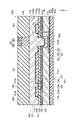
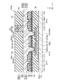
- FIG. 6 is a schematic cross-sectional view illustrating a part of the image display device according to the sixth embodiment. It is a schematic cross-sectional view which illustrates the manufacturing method of the image display apparatus of 6th Embodiment. It is a schematic cross-sectional view which illustrates the manufacturing method of the image display apparatus of 6th Embodiment. It is a schematic cross-sectional view which illustrates the manufacturing method of the image display apparatus of 6th Embodiment. It is a schematic cross-sectional view which illustrates the manufacturing method of the image display apparatus of 6th Embodiment. It is a schematic cross-sectional view which illustrates the manufacturing method of the image display apparatus of 6th Embodiment. It is a schematic cross-sectional view which illustrates the manufacturing method of the image display apparatus of 6th Embodiment.
- FIG. 6 is a schematic cross-sectional view illustrating a part of an image display device according to a modified example of the sixth embodiment. It is a schematic cross-sectional view which illustrates the manufacturing method of the image display apparatus of the modification of 6th Embodiment. It is a schematic cross-sectional view which illustrates the manufacturing method of the image display apparatus of the modification of 6th Embodiment. It is a schematic cross-sectional view which illustrates the manufacturing method of the image display apparatus of the modification of 6th Embodiment. It is a schematic cross-sectional view which illustrates the manufacturing method of the image display apparatus of the modification of 6th Embodiment. It is a schematic cross-sectional view which illustrates the manufacturing method of the image display apparatus of the modification of 6th Embodiment.
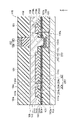
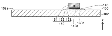
- FIG. 1 represents a cross section seen from an arrow on the AA'line of FIG. 4, which will be described later, and is a cross-sectional view in which cross sections in a plurality of planes perpendicular to the XY plane are connected on one plane. Also in other figures, as in FIG.
- the X-axis and the Y-axis are not shown, and the Z-axis perpendicular to the XY plane is shown. That is, in these figures, the plane perpendicular to the Z axis is the XY plane.
- the positive direction of the Z axis may be referred to as "up” or “upward”
- the negative direction of the Z axis may be referred to as "down” or “downward”. This is not always the case.
- the length in the direction along the Z axis may be referred to as height.
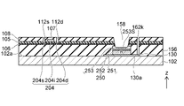
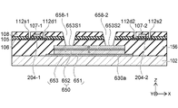
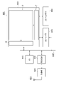
- the subpixel 20 has a light emitting surface 151S substantially parallel to the XY plane.
- the light emitting surface 151S is a surface that mainly emits light in the positive direction of the Z axis orthogonal to the XY plane.
- the subpixel 20 further includes a color filter 180.
- the color filter (wavelength conversion member) 180 is provided on the surface resin layer 170 via the transparent thin film adhesive layer 188.
- the surface resin layer 170 is provided on the second interlayer insulating film 108 and the wiring layer 110.
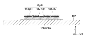
- the conductive layer 130 is provided on the first surface 102a.
- the conductive layer 130 includes a connection plate (first portion) 130a.
- the light emitting element 150 is provided on the connection plate 130a.
- the connection plate 130a is a member having a film-like, layer-like, or plate-like conductivity having a shape such as a square or an arbitrary polygon, an ellipse, or a circle in an XY plan view.
- the connection plate 130a is electrically connected to the light emitting element 150 at the bottom surface 153B of the light emitting element 150.
- connection plate 130a is provided for each subpixel 20.
- the different connection plates 130a may or may not be connected to each other in the conductive layer 130.
- the different connection plates 130a are connected to, for example, the power line 3 of FIG. 3, which will be described later, via vias 161a and wiring (first wiring) 110a provided for each connection plate 130a.
- Part or all of the conductive layer 130 is made of single crystal metal. It is preferable that the entire conductive layer 130 is formed of a single crystal metal layer. Part or all of the connecting plate 130a is made of single crystal metal. The portion of the connection plate 130a where the light emitting element 150 is provided is made of a single crystal metal, for example, forming a single crystal metal layer.
- the single crystal metal layer may be a part in the thickness direction including the surface to which the bottom surface 153B of the light emitting element 150 is connected.
- the outer circumference of the single crystal metal layer includes the outer circumference of the bottom surface 153B when projected onto the single crystal metal layer in XY plan view. That is, the outer circumference of the bottom surface 153B is arranged within the outer circumference of the single crystal metal.
- the area of the single crystal metal layer is larger than the area of the bottom surface 153B.
- the metal material forming the conductive layer 130 and the connection plate 130a is, for example, Cu, Hf, or the like.
- the metal material used for the conductive layer 130 and the connection plate 130a is not limited to Cu and Hf as long as it is a metal material that can be single-crystallized by an annealing treatment consistent with the LTPS process. Since the connection plate 130a is made of a metal material or the like, it has high conductivity and can be electrically connected to the light emitting element 150 with low resistance.
- the light emitting element 150 includes a bottom surface 153B and a light emitting surface 151S.
- the light emitting element 150 is a prismatic or columnar element having a bottom surface 153B on the connection plate 130a.
- the bottom surface 153B is provided on the connection plate 130a and is electrically connected to the connection plate 130a.
- the light emitting surface 151S is a surface opposite to the bottom surface 153B of the light emitting element 150.
- the outer circumference of the connection plate 130a is set to include the outer circumference of the light emitting element 150 when the light emitting element 150 is projected in XY plan view. That is, in XY plan view, the outer circumference of the light emitting element 150 is arranged within the outer circumference of the connection plate 130a.
- the conductive layer 130 and the connecting plate 130a are made of a metal material or the like as described above, and have light reflectivity. Therefore, the connection plate 130a reflects the scattered light downward of the light emitting element 150 toward the light emitting surface 151S side, and substantially improves the luminous efficiency of the light emitting element 150.
- the outer circumference of the connection plate 130a is set so as not to include the outer circumference of the transistor 103 when the transistor 103 is projected onto the plane including the connection plate 130a in XY plan view. That is, in the XY plan view, the outer circumference of the connection plate 130a is arranged outside the outer circumference of the transistor 103. By doing so, the transistor 103 is less likely to receive the reflected light from the connection plate 130a, and the probability of causing a malfunction can be sufficiently reduced.
- the outer circumference of the transistor 103 in the XY plane view is the outer circumference of the TFT channel 104 in the XY plane view, and the same applies to the embodiments and modifications described later.
- the light emitting element 150 includes a p-type semiconductor layer (first semiconductor layer) 153, a light emitting layer 152, and an n-type semiconductor layer (second semiconductor layer) 151.
- the p-type semiconductor layer 153, the light emitting layer 152, and the n-type semiconductor layer 151 are laminated in this order from the bottom surface 153B toward the light emitting surface 151S. Therefore, the p-type semiconductor layer 153 is electrically connected to the connection plate 130a.
- the shape of the light emitting element 150 in XY plane view is, for example, substantially a square or a rectangle.
- the shape of the light emitting element 150 in the XY plane view is a polygon including a square, the corners may be rounded.
- the shape of the light emitting element 150 in the XY plane view is a columnar shape, the shape of the light emitting element 150 in the XY plane view is not limited to a circle, and may be, for example, an ellipse.
- a gallium nitride based compound semiconductor including a light emitting layer such as In X Al Y Ga 1-XY N (0 ⁇ X, 0 ⁇ Y, X + Y ⁇ 1) is preferably used.
- the above-mentioned gallium nitride based compound semiconductor may be simply referred to as gallium nitride (GaN).
- the light emitting element 150 in one embodiment of the present invention is a so-called light emitting diode.
- the wavelength of the light emitted by the light emitting element 150 is, for example, about 467 nm ⁇ 30 nm.
- the wavelength of the light emitted by the light emitting element 150 may be bluish purple emission of about 410 nm ⁇ 30 nm.
- the wavelength of the light emitted by the light emitting element 150 is not limited to the above-mentioned value, and may be appropriate.
- the area of the light emitting layer 152 in the XY plane view is set according to the light emitting colors of the red, green, and blue subpixels.
- the area in the XY plane view may be simply referred to as an area.
- the area of the light emitting layer 152 is appropriately set by the visual sensitivity, the conversion efficiency of the color conversion unit 182 of the color filter 180, and the like. That is, the area of the light emitting layer 152 of the subpixel 20 of each light emitting color may be the same, or may be different for each light emitting color.
- the area of the light emitting layer 152 is the area of the area surrounded by the outer circumference of the light emitting layer 152 projected on the XY plane.
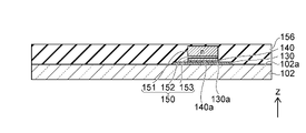
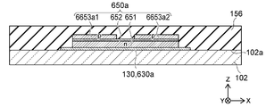
- the first interlayer insulating film (first insulating film) 156 covers the first surface 102a and the conductive layer 130.
- the first interlayer insulating film 156 covers the side surface of the light emitting element 150.
- the first interlayer insulating film 156 does not cover the light emitting surface 151S.
- the first interlayer insulating film 156 insulates the light emitting elements 150 from each other.
- the first interlayer insulating film 156 insulates the light emitting element 150 from a circuit element such as a transistor 103.
- the first interlayer insulating film 156 provides a flat surface for forming a circuit 101 including a circuit element such as a transistor 103.
- the first interlayer insulating film 156 protects the light emitting element 150 from thermal stress and the like when forming the transistor 103 and the like by covering the light emitting element 150.
- the first interlayer insulating film 156 is formed of an organic or inorganic insulating material.
- the insulating material used for the first interlayer insulating film 156 is preferably a white resin. Since the white resin reflects the lateral emission light of the light emitting element 150 and the return light caused by the interface of the color filter 180, it is necessary to use the white resin for the first interlayer insulating film 156 to improve the luminous efficiency of the light emitting element 150. Contributes to substantial improvement.
- the white resin is formed by dispersing scatterable fine particles having a Mie scattering effect in a silicon-based resin such as SOG (Spin On Glass) or a transparent resin such as a novolak-type phenol-based resin.
- the scattering fine particles are colorless or white, and have a diameter of about 1/10 to several times the wavelength of the light emitted by the light emitting element 150.
- the scatterable fine particles preferably used have a diameter of about 1 ⁇ 2 of the wavelength of light.
- examples of such scattering fine particles include TiO 2 , Al 2 O 3 , ZnO, and the like.
- the white resin can also be formed by utilizing a large number of fine pores dispersed in the transparent resin.
- a SiO 2 film formed by ALD (Atomic-Layer-Deposition) or CVD (Chemical Vapor Deposition) may be used on top of SOG or the like. ..
- the first interlayer insulating film 156 may be a black resin.
- the black resin as the first interlayer insulating film 156, the scattering of light in the subpixel 20 is suppressed, and the stray light is suppressed more effectively.
- An image display device in which stray light is suppressed can display a sharper image.
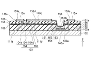
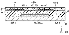
- the transistor 103 is formed on the TFT lower layer film 106.
- circuit elements such as other transistors and capacitors are formed on the TFT lower layer film 106, and the circuit 101 is formed by wiring or the like.
- the transistor 103 corresponds to the drive transistor 26 in FIG. 3, which will be described later.
- the selection transistor 24, the capacitor 28, and the like are circuit elements.
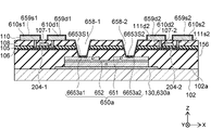
- the circuit 101 includes a TFT channel 104, an insulating layer 105, a second interlayer insulating film 108, vias 111s and 111d, and a wiring layer 110.
- the transistor 103 is an n-channel thin film transistor (TFT).
- the transistor 103 includes a TFT channel 104 and a gate 107.
- the TFT channel 104 is preferably formed by a Low Temperature Poly Silicon (LTPS) process.
- LTPS Low Temperature Poly Silicon
- the TFT channel 104 is formed by polycrystallizing and activating a region of amorphous Si formed on the TFT underlayer film 106. For example, laser annealing is used for polycrystallization and activation of the amorphous Si region.
- the TFT formed by the LTPS process has sufficiently high mobility.
- the TFT channel 104 includes regions 104s, 104i, 104d.
- the regions 104s, 104i, and 104d are all provided on the TFT underlayer film 106.
- the area 104i is provided between the area 104s and the area 104d.
- the regions 104s and 104d are doped with impurities such as phosphorus (P) by ion implantation or the like to form regions of an n-type semiconductor, and are ohmic-connected to the vias 111s and 111d.
- the gate 107 is provided on the TFT channel 104 via the insulating layer 105.
- the insulating layer 105 is provided to insulate the TFT channel 104 and the gate 107 and to insulate them from other adjacent circuit elements.
- a potential higher than the region 104s is applied to the gate 107, a channel is formed in the region 104i, so that the current flowing between the regions 104s and 104d can be controlled.
- the insulating layer 105 is, for example, SiO 2 .
- the insulating layer 105 may be a multi-layered insulating layer containing SiO 2 or Si 3 N 4 depending on the covering region.
- the gate 107 may be formed of, for example, polycrystalline Si or a refractory metal such as W or Mo.
- the polycrystalline Si film of the gate 107 is formed by, for example, CVD.
- the code of the wiring layer shall be displayed at the position next to one wiring included in the wiring layer to be labeled.
- the translucent electrode 159d is provided over the wiring 110d.
- the translucent electrode 159d is provided over the light emitting surface 151S.
- the translucent electrode 159d is also provided between the wiring 110d and the light emitting surface 151S, and electrically connects the wiring 110d and the light emitting surface 151S.
- the light emitting surface 151S is preferably roughened as in this example.
- the light emitting element 150 can improve the light extraction efficiency.
- the via 111s is provided between the wiring 110s and the area 104s, and electrically connects the wiring 110s and the area 104s.
- the via 111d is provided between the wiring 110d and the area 104d, and electrically connects the wiring 110d and the area 104d.
- the wiring 110s and the translucent electrode 159s are connected to the region 104s via the via 111s.
- the region 104s is the source region of the transistor 103. Therefore, the source region of the transistor 103 is electrically connected to the ground wire 4 via the via 111s, the wiring 110s, and the translucent electrode 159s.
- the wiring 110d and the translucent electrode 159d are connected to the region 104d via the via 111d.
- the region 104d is a drain region of the transistor 103. Therefore, the drain region of the transistor 103 is electrically connected to the n-type semiconductor layer 151 via the via 111d, the wiring (second wiring) 110d, and the translucent electrode 159d.
- the via 161a is provided so as to penetrate the second interlayer insulating film 108, the insulating layer 105, the TFT lower layer film 106, and the first interlayer insulating film 156.
- the via 161a is provided between the wiring 110a and the connection plate 130a, and electrically connects the wiring 110a and the connection plate 130a. Therefore, the p-type semiconductor layer 153 is electrically connected to, for example, the power line 3 of the circuit of FIG. 3 via the connection plate 130a, the via 161a, the wiring 110a, and the translucent electrode 159a.
- the wiring layer 110 and the vias 111s, 111d, 161a are formed of, for example, Al, Cu, or an alloy thereof. It may be formed by a laminated film of Al and Ti or the like. For example, in a laminated film of Al and Ti, Al is laminated on a thin film of Ti, and Ti is further laminated on Al.
- the surface resin layer 170 covers the second interlayer insulating film 108, the wiring layer 110, and the translucent electrodes 159s, 159d, 159a.
- the surface resin layer 170 is also filled in the opening 158.
- the surface resin layer 170 is provided on the light emitting surface 151S via the translucent electrode 159d.
- the surface resin layer 170 filled in the opening 158 is a translucent electrode provided so as to cover the side surfaces of the first interlayer insulating film 156, the TFT lower layer film 106, the insulating layer 105, and the second interlayer insulating film 108. It is provided on 159d.
- the surface resin layer 170 is a transparent resin, which protects the second interlayer insulating film 108, the wiring layer 110, and the translucent electrodes 159a, 159d, 159s, and provides a flattening surface for adhering the color filter 180. ..
- the color filter 180 includes a light-shielding unit 181 and a color conversion unit 182.
- the color conversion unit 182 is provided directly above the light emitting surface 151S of the light emitting element 150 according to the shape of the light emitting surface 151S.
- the portion other than the color conversion unit 182 is a light-shielding unit 181.
- the light-shielding unit 181 is a so-called black matrix, which reduces bleeding due to color mixing of light emitted from an adjacent color conversion unit 182 and makes it possible to display a sharp image.
- the color conversion unit 182 has one layer or two or more layers.
- FIG. 1 shows a case where the color conversion unit 182 has two layers. Whether the color conversion unit 182 has one layer or two layers is determined by the color of the light emitted by the subpixel 20, that is, the wavelength.
- the color conversion unit 182 is preferably two layers, a color conversion layer 183 and a filter layer 184 for passing red light.
- the color conversion unit 182 is preferably two layers, a color conversion layer 183 and a filter layer 184 for passing green light.
- the emission color of the subpixel 20 is blue, it is preferably one layer.
- the first layer is the color conversion layer 183 and the second layer is the filter layer 184.
- the first color conversion layer 183 is provided at a position closer to the light emitting element 150.
- the filter layer 184 is laminated on the color conversion layer 183.
- the color conversion layer 183 converts the wavelength of the light emitted by the light emitting element 150 into a desired wavelength.
- the light having a wavelength of 467 nm ⁇ 30 nm, which is the wavelength of the light emitting element 150 is converted into light having a wavelength of, for example, about 630 nm ⁇ 20 nm.
- light having a wavelength of 467 nm ⁇ 30 nm, which is the wavelength of the light emitting element 150 is converted into light having a wavelength of, for example, about 532 nm ⁇ 20 nm.
- the filter layer 184 blocks the wavelength component of blue light emission remaining without color conversion in the color conversion layer 183.
- the light emitting element 150 may output the light through the color conversion layer 183 or output the light as it is without passing through the color conversion layer 183. You may do so.
- the wavelength of the light emitted by the light emitting element 150 is about 467 nm ⁇ 30 nm, the light may be output without passing through the color conversion layer 183.
- the wavelength of the light emitted by the light emitting element 150 is 410 nm ⁇ 30 nm, it is preferable to provide one color conversion layer 183 in order to convert the wavelength of the output light to about 467 nm ⁇ 30 nm.
- the sub-pixel 20 may have a filter layer 184.
- the blue subpixel 20 may have a filter layer 184 through which blue light is transmitted, minute external light reflection other than blue light generated on the surface of the light emitting element 150 is suppressed.
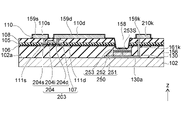
- FIG. 2 is a cross-sectional view schematically showing a part of an image display device according to a modified example of the present embodiment.
- the subpixel 20a is different from the case of the first embodiment described above in the connection method between the light emitting element 150a and the wiring 110d1.
- This modification is also different from the case of the first embodiment in that the translucent electrodes are not provided on the wirings 110s, 110d1, 110a.
- this modification is the same as in the first embodiment, and the same components are designated by the same reference numerals and detailed description thereof will be omitted as appropriate.
- FIG. 2 also shows the structure above the surface resin layer 170. These superstructures are also the same as in the case of the first embodiment.
- the subpixel 20a includes a light emitting element 150a and a wiring 110d1.
- a part of the wiring 110d1 is provided above the area 104d.
- the other part of the wiring 110d1 is provided so as to extend to the light emitting surface 151S, and the tip thereof is connected to the surface including the light emitting surface 151S.
- the surface including the light emitting surface 151S is a surface in the same plane as the light emitting surface 151S.
- the tip of the wiring 110d1 is connected to a surface other than the light emitting surface 151S on this surface.
- the light emitting surface 151S is not roughened, but may be roughened. When the surface is not roughened, the step for roughening can be omitted.
- FIG. 3 is a schematic block diagram illustrating an image display device according to the present embodiment.
- the image display device 1 of the present embodiment includes a display area 2.
- Subpixels 20 are arranged in the display area 2.
- the sub-pixels 20 are arranged in a grid pattern, for example. For example, n subpixels 20 are arranged along the X axis, and m subpixels 20 are arranged along the Y axis.
- Pixel 10 includes a plurality of sub-pixels 20 that emit light of different colors.
- the subpixel 20R emits red light.
- the subpixel 20G emits green light.
- the subpixel 20B emits blue light.
- the emission color and brightness of one pixel 10 are determined by the three types of sub-pixels 20R, 20G, and 20B emitting light at a desired brightness.
- the image display device 1 further includes a row selection circuit 5 and a signal voltage output circuit 7.
- the row selection circuit 5 and the signal voltage output circuit 7 are provided along the outer edge of the display area 2.
- the row selection circuit 5 is provided along the Y-axis direction of the outer edge of the display area 2.
- the row selection circuit 5 is electrically connected to the subpixels 20 in each column via the scanning line 6 to supply a selection signal to each subpixel 20.
- the signal voltage output circuit 7 is provided along the X-axis direction of the outer edge of the display area 2.
- the signal voltage output circuit 7 is electrically connected to the subpixel 20 of each line via the signal line 8 to supply a signal voltage to each subpixel 20.
- the subpixel 20 includes a light emitting element 22, a selection transistor 24, a drive transistor 26, and a capacitor 28.
- the selection transistor 24 may be displayed as T1
- the drive transistor 26 may be displayed as T2
- the capacitor 28 may be displayed as Cm.
- the light emitting element 22 is connected in series with the drive transistor 26.
- the drive transistor 26 is an n-channel TFT, and the cathode electrode of the light emitting element 22 is connected to the drain electrode of the drive transistor 26.
- the main electrodes of the drive transistor 26 and the selection transistor 24 are a drain electrode and a source electrode.
- the anode electrode of the light emitting element 22 is connected to the p-type semiconductor layer.
- the cathode electrode of the light emitting device is connected to the n-type semiconductor layer.
- the series circuit of the light emitting element 22 and the drive transistor 26 is connected between the power supply line 3 and the ground line 4.
- the drive transistor 26 corresponds to the transistor 103 in FIG.
- the light emitting element 22 corresponds to the light emitting element 150 in FIG.
- the current flowing through the light emitting element 22 is determined by the voltage applied between the gate and the source of the drive transistor 26, and the light emitting element 22 emits light with a brightness corresponding to the flowing current.
- the selection transistor 24 is connected between the gate electrode of the drive transistor 26 and the signal line 8 via a main electrode.
- the gate electrode of the selection transistor 24 is connected to the scanning line 6.
- a capacitor 28 is connected between the gate electrode of the drive transistor 26 and the power supply line 3.
- the row selection circuit 5 selects one row from the array of subpixels 20 in the m row and supplies the selection signal to the scanning line 6.
- the signal voltage output circuit 7 supplies a signal voltage having the required analog voltage value for each subpixel 20 in the selected row.
- a signal voltage is applied between the gate and the source of the drive transistor 26 of the subpixel 20 in the selected row.
- the signal voltage is held by the capacitor 28.
- the drive transistor 26 causes a current corresponding to the signal voltage to flow through the light emitting element 22.
- the light emitting element 22 emits light with a brightness corresponding to the flowing current.
- the anode electrode of the light emitting element 150 is arranged on the connection plate 130a and is electrically connected to the connection plate 130a.
- the connection plate 130a is provided below the transistor 103 and the wiring layer 110 shown in FIG.
- the connection plate 130a is electrically connected to the wiring 110a via the via 161a. More specifically, one end of the via 161a is connected to the connection plate 130a, and the other end of the via 161a is connected to the wiring 110a via the contact hole 161a1.
- the cathode electrode of the light emitting element 150 is provided by the n-type semiconductor layer 151 shown in FIG.
- the wiring 110d is covered with the translucent electrode 159d shown in FIG.
- the translucent electrode 159d covers the light emitting surface 151S. Since the translucent electrode 159d is also provided between the wiring 110d and the light emitting surface 151S, the cathode electrode of the light emitting element 150 is electrically connected to the wiring 110d.
- a part of the wiring 110d is connected to the drain electrode of the transistor 103 via the via 111d.
- the drain electrode of the transistor 103 is the region 104d shown in FIG.
- the source electrode of the transistor 103 is connected to the wiring 110s via the via 111s.
- the source electrode of the transistor 103 is the region 104s shown in FIG.
- the wiring layer 110 includes a ground wire 4, and the wiring 110s is connected to the ground wire 4.
- the power line 3 is provided in a layer higher than the wiring layer 110.
- an interlayer insulating film is further provided on the wiring layer 110.
- the power line 3 is provided on the interlayer insulating film of the uppermost layer, and is insulated from the ground line 4.
- the light emitting element 150 can be electrically connected to the wiring 110a provided on the upper layer of the light emitting element 150 by using the via 161a. Further, the light emitting element 150 exposes the light emitting surface 151S through the opening 158, and by providing the translucent electrode 159d over the opening 158, the transistor 103 provided above the light emitting element 150 via the wiring 110d. Can be electrically connected to.
- FIG. 5A to 7B are schematic cross-sectional views illustrating the manufacturing method of the image display device of the present embodiment.
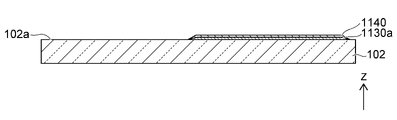
- a substrate (first substrate) 102 is prepared.
- the substrate 102 is a translucent substrate, for example, a substantially rectangular glass substrate having a size of about 1500 mm ⁇ 1800 mm.
- the conductive layer 1130 is formed on the first surface 102a.
- the conductive layer (metal layer) 1130 is patterned so as to leave a portion where a light emitting layer is formed after forming a layer of a metal material on the entire surface of the first surface 102a by sputtering or the like.
- the conductive layer 1130 may be provided with a mask having a pattern that opens a portion where the light emitting layer is formed on the first surface 102a, and then the patterned conductive layer 1130 may be formed.
- the conductive layer 1130 is formed by using a metal material such as Cu or Hf.
- a metal material such as Cu or Hf.
- sputtering or the like is preferably used in order to form a film at a low temperature.
- the patterned conductive layer 1130 is single crystallized by an annealing treatment.
- the annealing treatment is applied so as to be single crystallized over the entire patterned conductive layer 1130.
- an annealing treatment by laser irradiation is preferably used.
- the conductive layer 1130 can be single-crystallized in a state where the influence of the temperature on the layer below the conductive layer 1130 is suppressed to a low temperature of about 400 ° C. to about 500 ° C., so that the substrate 102 is made of glass or an organic resin described later.
- a flexible substrate or the like can be used.
- the semiconductor layer 1150 is formed over the single crystallized conductive layer 1130a.
- the semiconductor layer 1150 is formed in the order of the p-type semiconductor layer 1153, the light emitting layer 1152, and the n-type semiconductor layer 1151 from the conductive layer 1130a in the positive direction of the Z axis.
- a physical vapor deposition method such as thin film deposition, ion beam deposition, molecular beam epitaxy (MBE) or sputtering is used, and a low temperature sputtering method is preferably used.
- MBE molecular beam epitaxy
- a low temperature sputtering method it is preferable to assist with light or plasma at the time of film formation because the temperature can be lowered.
- Epitaxy growth by MOCVD may exceed 1000 ° C.
- a GaN crystal containing a light emitting layer can be epitaxially grown on a single crystal metal layer at a low temperature of about 400 ° C to 700 ° C (Non-Patent Document 1). See 2nd class).
- Such a low temperature sputtering method is consistent with forming the semiconductor layer 1150 on a circuit board having a TFT or the like formed by the LTPS process.
- Layer 1150 is formed.
- amorphous deposits containing Ga or the like which is a material for growing species, may be deposited in a place where the conductive layer 1130a does not exist.
- the conductive layer 1130a of a single crystal metal is used as a seed to promote the crystal formation of GaN.
- a conductive buffer layer is provided on the conductive layer 1130a, and the semiconductor layer is formed on the buffer layer by the above-mentioned low-temperature sputtering method or the like. You may try to grow it.
- the buffer layer may be of any type as long as it is a material that promotes GaN crystal formation. Graphene sheets in the case of other embodiments described later may be used.
- the semiconductor layer 1150 shown in FIG. 5B is formed into a desired shape by etching or the like, and a light emitting element 150 is formed.
- a dry etching process is used for forming the light emitting element 150, and anisotropic plasma etching (Reactive Ion Etching, RIE) is preferably used.
- RIE reactive Ion Etching
- the conductive layer 130 is formed by etching the conductive layer 1130a shown in FIG. 5B.
- the connection plate (first portion) 130a is formed.
- the conductive layer 1130a may be etched together with the semiconductor layer 1150 to form the connection plate 130a, and then the light emitting device 150 may be formed.
- the connection plate 130a is formed on the first surface 102a, and the light emitting element 150 is formed on the connection plate 130a.
- the outer circumference of the connection plate 130a is set to include the outer circumference of the light emitting element 150 when the light emitting element 150 is projected in XY plan view. That is, in XY plan view, the outer circumference of the light emitting element 150 is arranged within the outer circumference of the connection plate 130a.
- the TFT channel (circuit element) 104 is formed on the TFT underlayer film 106.
- the TFT channel 104 is formed as follows. First, amorphous Si is formed into the shape of the TFT channel 104. For example, CVD or the like is used for forming an amorphous Si film. The formed amorphous Si film is polycrystallized by laser annealing to form a TFT channel 104.
- the via hole 162a is formed so as to penetrate the second interlayer insulating film 108, the insulating layer 105, the TFT lower layer film 106, and the first interlayer insulating film 156 and reach the connection plate 130a.
- the opening 158 reaches the light emitting surface 151S by removing a part of the second interlayer insulating film 108, a part of the insulating layer 105, a part of the TFT lower layer film 106, and a part of the first interlayer insulating film 156. Is formed in.
- the via hole 112d is formed so as to penetrate the second interlayer insulating film 108 and the insulating layer 105 and reach the region 104d.
- the via hole 112s is formed so as to penetrate the second interlayer insulating film 108 and the insulating layer 105 and reach the region 104s.
- RIE is used for forming the via holes 162a, 112d, 112s and the opening 158.
- the via 161a is formed by filling the via hole 162a shown in FIG. 7A with a conductive material.
- the vias 111d and 111s are also formed by filling the via holes 112d and 112s shown in FIG. 7A with a conductive material, respectively.
- the wiring layer 110 including the wirings 110a, 110d, 110s is formed on the second interlayer insulating film 108.
- the wirings 110a, 110d, 110s are connected to the vias 161a, 111d, 111s, respectively.
- the wiring layer 110 may be formed at the same time as the vias 161a, 111d, 111s are formed.
- the translucent conductive film is formed on the wiring layer 110 and the second interlayer insulating film 108, and the translucent electrodes 159a, 159d, 159s are formed.
- the sub-pixel 20 of the image display device 1 of the present embodiment is formed by providing a color filter (wavelength conversion member) 180 or the like.
- FIGS. 8A and 8B are schematic cross-sectional views illustrating a method for manufacturing an image display device according to a modified example of the present embodiment.
- 8A and 8B show a process for forming the subpixel 20a shown in FIG.
- the steps up to the step shown in FIG. 6B for forming the TFT channel 104, the insulating layer 105, and the gate 107 and forming the second interlayer insulating film 108 covering them are the same as those described above. There is.
- the steps of FIGS. 8A and 8B will be described as being applied to the steps after the steps shown in FIG. 6B.
- via holes 162a, 112d, 112s are formed.
- the opening 158 is formed so as to reach the n-type semiconductor layer 151a.
- the etching step for roughening can be omitted.
- the vias 161a, 111d, 111s are formed by filling the via holes 162a, 112d, 112s shown in FIG. 8A with a conductive material.
- the wiring layer 110 is formed, and the wirings 110a, 110d1, 110s are formed.
- one end of the wiring 110d1 is connected to the via 111d.
- the wiring 110d1 is provided so as to extend from the position connected to the via 111d to the light emitting surface 151S.
- the other end of the wiring 110d1 is connected to a surface including the light emitting surface 151S. That is, the surface including the light emitting surface 151S is the n-type semiconductor layer 151a, and the wiring 110d1 is directly connected to the n-type semiconductor layer 151a.
- the sub-pixel 20a of this modification is formed by providing the color filter 180 or the like.
- the signal voltage output circuit 7 be incorporated in a semiconductor device manufactured by a manufacturing process capable of high integration by microfabrication.
- the signal voltage output circuit 7 is mounted on another board together with the CPU and other circuit elements, and is provided, for example, before the incorporation of the color filter described later, or after the incorporation of the color filter, for example, at the peripheral edge of the display area. It is interconnected with the sub-pixels 20 and 20a via a connector or the like.
- FIG. 9 is a schematic cross-sectional view illustrating the method for manufacturing the image display device of the present embodiment.
- the figure above the arrow shows the configuration including the color filter 180
- the figure below the arrow shows the structure including the light emitting element 150 and the like formed in the above-mentioned steps.
- FIG. 9 shows a step of adhering a color filter to a structure including a light emitting element 150 and the like by an arrow.
- the display of components other than the components on the illustrated substrate 102 is omitted.
- the omitted components are the circuit 101 including the TFT channel 104, the wiring layer 110, and the like shown in FIG. 1, and the via 161a.
- FIGS. 9 is a schematic cross-sectional view illustrating the method for manufacturing the image display device of the present embodiment.
- the figure above the arrow shows the configuration including the color filter 180
- the figure below the arrow shows the structure including the light emitting element 150 and the like formed in the above-mentioned steps.
- the structure including the light emitting element 150, the first interlayer insulating film 156, the TFT lower layer film 106, the insulating layer 105, the second interlayer insulating film 108, and the surface resin layer 170 is included. It is called a light emitting circuit unit 172.
- a structure including a substrate 102, a conductive layer 130, a light emitting circuit unit 172, and components whose display is omitted is referred to as a structure 1192.
- the TFT channel 104, the gate 107, the vias 111s, 111d, and the wiring layer 110 are not shown.
- the color filter (wavelength conversion member) 180 is adhered to the structure 1192 on one side.
- the other surface of the color filter 180 is adhered to the glass substrate 186.
- a transparent thin film adhesive layer 188 is provided on one surface of the color filter 180, and is adhered to the exposed surface of the surface resin layer 170 of the structure 1192 via the transparent thin film adhesive layer 188.
- the color filter 180 has color conversion units arranged in the positive direction of the X-axis in the order of red, green, and blue.
- a red color conversion layer 183R is provided on the first layer
- a green color conversion layer 183G is provided on the first layer
- a filter layer 184 is provided on the second layer in each case.
- Each is provided.
- a single-layer color conversion layer 183B may be provided, or a filter layer 184 may be provided.
- a light-shielding unit 181 is provided between the color conversion units, and the frequency characteristics of the filter layer 184 can be changed for each color of the color conversion unit.
- the color conversion layer 183 be as thick as possible in order to improve the color conversion efficiency.
- the color conversion layer 183 is too thick, the emitted light of the color-converted light is approximated to Lambersian, whereas the emission angle of the non-color-converted blue light is limited by the light-shielding portion 181. .. Therefore, there arises a problem that the display color of the display image is dependent on the viewing angle.
- the thickness of the color conversion layer 183 should be about half the opening size of the light-shielding portion 181. Is desirable.
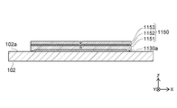
- FIG. 11 is a schematic perspective view illustrating the image display device according to the present embodiment.
- a light emitting circuit unit 172 having a large number of subpixels 20 is provided on the substrate 102.
- the conductive layer 130 shown in FIG. 9 includes a connection plate 130a.
- the connection plate 130a is provided on the substrate 102 according to each of the subpixels 20.
- a color filter 180 is provided on the light emitting circuit unit 172.
- Other embodiments and modifications described later have the same configurations as those shown in FIG. 11.
- the light emitting element 150 is formed by etching the semiconductor layer 1150 in which crystals are grown on the substrate 102. After that, the light emitting element 150 is covered with the first interlayer insulating film 156, and a circuit 101 including a circuit element such as a transistor 103 for driving the light emitting element 150 is built on the first interlayer insulating film 156. Therefore, the manufacturing process is remarkably shortened as compared with transferring the individualized light emitting elements to the substrate 102 individually.
- the number of sub-pixels exceeds 24 million, and in the case of an 8K image quality image display device, the number of sub-pixels exceeds 99 million. It would take an enormous amount of time to individually form such a large number of light emitting elements and mount them on a circuit board. Therefore, it is difficult to realize an image display device using micro LEDs at a realistic cost. Further, if a large number of light emitting elements are individually mounted, the yield is reduced due to poor connection at the time of mounting, and further cost increase is unavoidable.
- the glass substrate formed as described above is covered with an interlayer insulating film, and a drive circuit including a TFT or the like, a scanning circuit, or the like is formed on the flattened surface by using an LTPS process or the like. Can be done. Therefore, there is an advantage that the existing flat panel display manufacturing process and plant can be used.
- the conductive layer 130 is formed on the first surface 102a of the substrate 102.
- the conductive layer 130 includes a connection plate 130a.
- the light emitting element 150 is formed on the connection plate 130a and is electrically connected to the connection plate 130a at the bottom surface 153B.
- the connection plate 130a is made of a highly conductive material such as a metal material. Therefore, the p-type semiconductor layer 153 of the light emitting element 150 can be electrically connected to another circuit with low resistance.
- connection plate 130a can be formed of a metal material having light reflectivity such as Cu or Hf.
- the outer periphery of the connection plate 130a is formed so as to include the outer periphery of the light emitting element 150 when the light emitting element 150 is projected in XY plan view. That is, in XY plan view, the outer circumference of the light emitting element 150 is arranged within the outer circumference of the connection plate 130a. Therefore, the connection plate 130a also functions as a light reflecting plate, and can substantially improve the luminous efficiency of the light emitting element 150 by reflecting the scattered light or the like downward of the light emitting element 150 on the light emitting surface 151S.
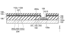
- FIG. 12 is a schematic cross-sectional view illustrating a part of the image display device according to the present embodiment.
- the p-type semiconductor layer 253 provides the light emitting surface 253S and the configuration of the transistor 203 is different from that of the other embodiments described above.
- the same components as in the case of other embodiments are designated by the same reference numerals, and detailed description thereof will be omitted as appropriate.
- the subpixel 220 of the image display device of the present embodiment includes a substrate 102, a conductive layer 130, a light emitting element 250, a first interlayer insulating film 156, a transistor 203, and a second interlayer insulation.
- the film 108 and the wiring layer 110 are included.
- the light emitting element 250 is provided on the connection plate 130a.
- the outer circumference of the connection plate 130a is set to include the outer circumference of the light emitting element 250 when the light emitting element 250 is projected in XY plan view. That is, in XY plan view, the outer circumference of the light emitting element 250 is arranged within the outer circumference of the connection plate 130a. Therefore, the light scattered downward of the light emitting element 250 can be reflected to the light emitting surface 253S side, and the luminous efficiency of the light emitting element 250 is substantially improved as in the case of the other embodiments described above. Is.
- the light emitting element 250 includes an n-type semiconductor layer 251, a light emitting layer 252, and a p-type semiconductor layer 253.
- the n-type semiconductor layer 251 and the light emitting layer 252 and the p-type semiconductor layer 253 are laminated in this order from the bottom surface 251B toward the light emitting surface 253S.
- the light emitting surface 253S is provided by the p-type semiconductor layer 253.
- the light emitting element 250 is a light emitting diode similar to the light emitting element 150 of the other embodiment described above. That is, the wavelength of the light emitted by the light emitting element 250 is, for example, blue light emission of about 467 nm ⁇ 30 nm or blue-purple light emission of about 410 nm ⁇ 30 nm.
- the wavelength of the light emitted by the light emitting element 250 is not limited to the above-mentioned value, and may be appropriate.
- the via 161k is provided so as to penetrate the second interlayer insulating film 108, the insulating layer 105, the TFT lower layer film 106, and the first interlayer insulating film 156.
- the via 161k is provided between the wiring 210k and the connection plate 130a, and electrically connects the wiring 210k and the connection plate 130a.
- the wiring 110s is electrically connected to, for example, the power line 3 shown in FIG. 13, which will be described later.
- the wiring 110d is electrically connected to the p-type semiconductor layer 253 via the translucent electrode 159d.
- the translucent electrode 159d is provided over the light emitting surface 253S of the roughened p-type semiconductor layer 253.
- the translucent electrode 159d is provided over the wiring 110d.
- the translucent electrode 159d is also provided between the light emitting surface 253S and the wiring 110d, and electrically connects the p-type semiconductor layer 253 and the wiring 110d.
- the wiring 110d1 may be extended and directly connected to the p-type semiconductor layer 253 as in the example shown in FIG.
- FIG. 13 is a schematic block diagram illustrating an image display device according to the present embodiment.
- the image display device 201 of the present embodiment includes a display area 2, a row selection circuit 205, and a signal voltage output circuit 207.
- the sub-pixels 220 are arranged in a grid pattern on the XY plane, as in the case of the other embodiments described above.
- Pixel 10 includes a plurality of sub-pixels 220 that emit light of different colors, as in the case of the other embodiments described above.
- the subpixel 220R emits red light.
- the subpixel 220G emits green light.
- the sub-pixel 220B emits blue light.
- the emission color and brightness of one pixel 10 are determined by the three types of sub-pixels 220R, 220G, and 220B emitting light at a desired brightness.
- One pixel 10 includes three sub-pixels 220R, 220G, 220B, and the sub-pixels 220R, 220G, 220B are linearly arranged on the X-axis, for example, as in this example.
- sub-pixels of the same color may be arranged in the same column, or sub-pixels of different colors may be arranged in each column as in this example.
- the subpixel 220 includes a light emitting element 222, a selection transistor 224, a drive transistor 226, and a capacitor 228.
- the selection transistor 224 may be displayed as T1
- the drive transistor 226 may be displayed as T2
- the capacitor 228 may be displayed as Cm.
- a selection transistor 224 is connected between the gate electrode of the drive transistor 226 and the signal line 208.
- the capacitor 228 is connected between the gate electrode of the drive transistor 226 and the power line 3.
- the row selection circuit 205 and the signal voltage output circuit 207 supply a signal voltage having a polarity different from that of the other embodiment described above to the signal line 208 in order to drive the drive transistor 226 which is a transistor of the p channel.
- the row selection circuit 205 supplies a selection signal to the scanning line 206 so as to sequentially select one row from the array of subpixels 220 in the m row.
- the signal voltage output circuit 207 supplies a signal voltage having the required analog voltage value for each subpixel 220 in the selected row.
- the drive transistor 226 of the subpixel 220 in the selected row causes a current corresponding to the signal voltage to flow through the light emitting element 222.
- the light emitting element 222 emits light with a brightness corresponding to the current flowing through the light emitting element 222.
- FIG. 14A to 16B are schematic cross-sectional views illustrating the manufacturing method of the image display device of the present embodiment.
- the substrate 102 in which the conductive layer 1130 described in relation to FIG. 5A of the other embodiment described above is formed on the first surface 102a can be used.
- the steps after FIG. 14A will be described as being applied after the step of FIG. 5A.
- the conductive layer 1130 shown in FIG. 5A is subjected to a single crystallization treatment and is single crystallized on the first surface 102a.
- Layer 1130a is formed.
- the semiconductor layer 1150 is formed on the conductive layer 1130a.
- the semiconductor layer 1150 is formed in the order of the n-type semiconductor layer 1151, the light emitting layer 1152, and the p-type semiconductor layer 1153 from the conductive layer 1130a in the positive direction of the Z axis.
- the semiconductor layer 1150 is formed by using the same film forming technique as in the case of the other embodiments described above. That is, the low temperature sputtering method is preferably used for forming the semiconductor layer 1150, and other physical vapor deposition methods such as thin film deposition, ion beam deposition, and MBE are used.
- the semiconductor layer 1150 shown in FIG. 14A is formed into a desired shape, and a light emitting element 250 is formed.
- a dry etching process is used, and RIE is preferably used.
- the first interlayer insulating film 156 is formed so as to cover the first surface 102a, the conductive layer 130, and the light emitting element 250.
- the TFT lower layer film 106 is formed over the exposed surface of the first interlayer insulating film 156.
- CVD or the like is used to form the TFT underlayer film 106.
- the TFT channel 204 is formed at a predetermined position on the TFT underlayer film 106 and is activated or the like.
- the insulating layer 105 is formed over the TFT underlayer film 106 and the TFT channel 204.
- the gate 107 is formed on the TFT channel 204 via the insulating layer 105.
- the LTPS process is preferably used as the above forming process.
- the second interlayer insulating film 108 is formed over the insulating layer 105 and the gate 107.
- the via hole 162k is formed so as to penetrate the second interlayer insulating film 108, the insulating layer 105, the TFT lower layer film 106, and the first interlayer insulating film 156 and reach the connection plate 130a.
- the opening 158 reaches the light emitting surface 253S by removing a part of the second interlayer insulating film 108, a part of the insulating layer 105, a part of the TFT lower layer film 106, and a part of the first interlayer insulating film 156. Is formed in.
- the central portion of the surface of the p-type semiconductor layer 253 exposed by removing the first interlayer insulating film 156 and the like is etched in the thickness direction of the p-type semiconductor layer 253, and the light emitting surface 253S is used.
- the light emitting surface 253S is preferably roughened as in the case of the other embodiments described above.
- the vias 161k, 111d, 111s are formed by filling the via holes 162k, 112d, 112s shown in FIG. 16A with a conductive material.
- the wiring layer 110 including the wirings 210k, 110d, 110s is subsequently formed, and the wirings 210k, 110d, 110s are connected to the vias 161k, 111d, 111s, respectively.
- the sub-pixel 220 of the image display device 201 of the present embodiment is formed by providing the color filter 180 or the like.
- FIG. 17 is a schematic cross-sectional view illustrating a part of the image display device according to the present embodiment.
- This embodiment differs from the other embodiments described above in that the graphene layer 140 is provided on the conductive layer 130 and the graphene sheet 140a is provided between the connection plate 130a and the light emitting element 150. ..
- the same components as in the case of the other embodiments described above are designated by the same reference numerals, and detailed description thereof will be omitted as appropriate.
- the graphene sheet 140a has an outer circumference that substantially coincides with the outer circumference of the light emitting element 150 in XY plan view.
- the light emitting element 150 is configured in the same manner as in the case of the first embodiment. That is, the p-type semiconductor layer 153, the light emitting layer 152, and the n-type semiconductor layer 151 are laminated in this order from the bottom surface 153B toward the light emitting surface 151S.
- the bottom surface 153B is a p-type semiconductor layer 153, and the p-type semiconductor layer 153 is electrically connected to the connection plate 130a via the graphene sheet 140a.
- the light emitting surface 151S is roughened, but the roughening can be omitted.
- the effect of the image display device of this embodiment will be described.
- the light emitting element 150 is formed via the graphene sheet 140a formed on the connection plate 130a of the single crystal metal. Therefore, the image display device of the present embodiment can obtain a light emitting element 150 having a higher quality crystal structure. Therefore, the yield of the image display device can be improved.
- FIG. 21 is a schematic cross-sectional view illustrating a part of the image display device according to the present embodiment.
- the via 461a is different from the case of the first embodiment in that the via 461a is provided between the connection plate 130a and the wiring 410d.
- the light emitting element 150 is also different from the case of the first embodiment in that it is driven by the p-type transistor 203.
- the same components as in the other embodiments described above are designated by the same reference numerals, and detailed description thereof will be omitted as appropriate.
- connection plate 130a is provided as in the case of the first embodiment. That is, the connection plate 130a is provided directly below the light emitting element 150, and the outer periphery of the connection plate 130a includes the outer periphery of the light emitting element 150 when the light emitting element 150 is projected onto the connection plate 130a in XY plan view. Is set to. That is, in XY plan view, the outer circumference of the light emitting element 150 is arranged within the outer circumference of the connection plate 130a. Therefore, the connection plate 130a also functions as a light reflection plate, and substantially improves the luminous efficiency of the light emitting element 150.
- the translucent electrode 159k is provided over the wiring 410k.
- the translucent electrode 159k is provided over the light emitting surface 151S.
- the translucent electrode 159k is provided between the wiring 410k and the light emitting surface 151S. Therefore, the n-type semiconductor layer 151 is electrically connected to, for example, the ground wire 4 of the circuit shown in FIG. 13 via the translucent electrode 159k and the wiring (fourth wiring) 410k.
- the vias 461a, 111d, 111s and wirings 410k, 410d, 110s are formed of the same materials and manufacturing methods as in the case of the above-mentioned other embodiments and modifications thereof.
- the via hole 462a is formed so as to penetrate the second interlayer insulating film 108, the insulating layer 105, the TFT lower layer film 106, and the first interlayer insulating film 156 and reach the connection plate 130a.
- the openings 158 and the via holes 112d, 112s are formed in the same manner as in the other embodiments described above.
- the via holes 462a, 112d, 112s shown in FIG. 22A are filled with a conductive material, and vias 461a, 111d, 111s are formed.
- the wiring layer 110 is formed on the second interlayer insulating film 108.
- a translucent conductive film is formed on the wiring layer 110, and translucent electrodes 159k, 159d, and 159s are formed.
- the effect of the image display device of this embodiment will be described.
- the image display device of the present embodiment has the following effects in addition to the effects of the first embodiment described above. That is, in the present embodiment, it is possible to have a circuit configuration in which the light emitting element 150 is driven by the transistor 203 of the p channel while the light emitting surface 151S is the n-type semiconductor layer 151. Therefore, flexible circuit design is possible by expanding variations such as circuit layout.
- the image display device of the present embodiment includes subpixels 520.
- Subpixel 520 includes a substrate 502.
- the substrate 502 includes a first surface 502a.
- a layer 507 containing a silicon compound is formed on the first surface 502a.
- the layer 507 containing the silicon compound is formed of SiO 2 , SiN x , or the like. Since the conductive layer 130 is made of a metal material, the layer 507 containing the silicon compound is provided in order to improve the adhesion between the substrate 502 and the conductive layer 130.
- the conductive layer 130 and the connection plate 130a are provided on the first surface 502a via a layer 507 containing a silicon compound.
- a layer 507 containing a silicon compound the structure and components above the conductive layer 130 and the connection plate 130a are the same as in the first embodiment described above, and detailed description thereof will be omitted.
- the substrate 502 has flexibility.
- the substrate 502 is made of, for example, a polyimide resin or the like.
- the first interlayer insulating film 156, the second interlayer insulating film 108, the wiring layer 110, and the like are preferably formed of a material having a certain degree of flexibility depending on the flexibility of the substrate 502.
- the wiring layer 110 having the longest wiring length has the highest risk of being destroyed during bending.
- the inner surface that bends when the image display device is bent is reduced by receiving compressive stress, and the outer surface is stretched by receiving elongation stress.
- a neutral surface in which both stresses cancel each other exists inside the image display device, and the neutral surface does not expand or contract due to stress due to bending.
- a plurality of protective films may be provided on the front surface or the back surface of the image display device to reduce the stress due to bending. Further, it is desirable to adjust the film thickness, film quality, material, etc. of these protective films so that the neutral surface overlaps with the position of the wiring layer 110.
- the structure and components above the layer 507 containing the silicon compound are the same as in the first embodiment, but may be other embodiments or modifications described above. Further, in the case of the sixth embodiment described later, it is also possible to apply the flexible substrate 502 in the case of the present embodiment.
- FIG. 24A and 24B are schematic cross-sectional views illustrating the method of manufacturing the image display device of the present embodiment.
- the substrate 1002 includes two layers of substrates 102 and 502.
- the substrate (first substrate) 102 is, for example, a glass substrate.
- the substrate (second substrate) 502 is provided on the first surface 102a of the substrate 102.
- the substrate 502 is formed by applying polyimide on the first surface 102a and firing it.
- an inorganic film such as SiN x may be formed on the first surface 102a.
- the substrate 502 is formed by applying a polyimide material on an inorganic film and firing it.
- a layer 507 containing a silicon compound is formed over the first surface 502a of the substrate 502.
- the first surface 502a of the substrate 502 is a surface opposite to the surface on which the substrate 102 is provided.
- the conductive layer 1130 is formed and patterned on the exposed surface of the layer 507 containing the silicon compound formed on the substrate 1002. Then, for example, by applying the steps described above in FIGS. 5B-7B, 9 and 10A-10D, the superstructure of the subpixel 520 is formed.
- the removal of the substrate 102 is not limited to the above-mentioned time point, but can be performed at an appropriate time point.
- the substrate 102 is preferably removed after the step of forming the wiring layer 110 is completed. By removing the substrate 102 at an appropriate time, it may be possible to reduce defects such as cracks and chips in the manufacturing process.
- the effect of the image display device of this embodiment will be described.
- the image display device of this embodiment has the following effects in addition to the effects of the other embodiments described above. That is, since the substrate 502 has flexibility, it can be bent as an image display device, and can be attached to a curved surface, used for a wearable terminal, or the like without any discomfort.
- FIG. 25 is a schematic cross-sectional view illustrating a part of the image display device according to the present embodiment.
- a plurality of light emitting surfaces 653S1 and 653S2 on a single semiconductor layer 650 including a light emitting layer, an image display device having higher luminous efficiency is realized.
- the same components as in the case of the other embodiments described above are designated by the same reference numerals, and detailed description thereof will be omitted as appropriate.
- the conductive layer 130 and the connection plate 630a are connected to, for example, the ground wire 4 of the circuit of FIG.
- the transistors 203-1 and 203-2 of the p-channel electrons are injected from one of the semiconductor layers 650 via the conductive layer 130 and the connection plate 130a.
- the transistors 203-1 and 203-2 of the p-channel holes are injected from the other side of the semiconductor layer 650 via the wiring layer 110. Holes and electrons are injected into the semiconductor layer 650, and the light emitting layer 652 is made to emit light by the combination of holes and electrons.
- the conductive layer 130 is provided on the first surface 102a.
- the conductive layer 130 includes a connection plate 630a.
- the semiconductor layer 650 is provided on the first surface 102a via the connection plate 630a.
- the semiconductor layer 650 has a bottom surface 651B, and the connection plate 630a is connected to the bottom surface 651B.
- the outer circumference of the connection plate 630a is set to include the outer circumference of the semiconductor layer 650 when the semiconductor layer 650 is projected onto the connection plate 630a in XY plan view. That is, in the XY plan view, the outer circumference of the semiconductor layer 650 is arranged within the outer circumference of the connection plate 630a.
- connection plate 630a Since the conductive layer 130 and the connection plate 630a are made of a metal material such as Cu or Hf, they have light reflectivity. Therefore, the connection plate 630a reflects the downward scattered light of the semiconductor layer 650 toward the upper light emitting surfaces 653S1 and 653S2. Therefore, the substantial luminous efficiency of the semiconductor layer 650 is improved.
- the semiconductor layer 650 includes a plurality of light emitting surfaces 653S1 and 653S2.
- the semiconductor layer 650 is a prismatic or columnar laminate having a bottom surface 651B connected to the connection plate 630a.
- the light emitting surfaces 653S1 and 653S2 are surfaces on the opposite side of the bottom surface 651B.
- the light emitting surfaces 653S1 and 653S2 are preferably planes in a plane substantially parallel to the bottom surface 651B.
- the plane including the light emitting surface 653S1 and the plane including the light emitting surface 653S2 may be the same plane or different planes.
- the light emitting surfaces 653S1 and 653S2 are provided apart from each other in the X-axis direction.
- the semiconductor layer 650 includes an n-type semiconductor layer 651, a light emitting layer 652, and a p-type semiconductor layer 653.
- the n-type semiconductor layer 651, the light emitting layer 652, and the p-type semiconductor layer 653 are laminated in this order from the bottom surface 651B toward the light emitting surfaces 653S1 and 653S2.
- the bottom surface 651B is an n-type semiconductor, and the n-type semiconductor layer 651 is electrically connected to an external circuit connected via the bottom surface 651B and the connection plate 630a.
- the external circuit is, for example, the ground wire 4 of the circuit of FIG.
- the p-type semiconductor layer 653 has two light emitting surfaces 653S1 and 653S2 on the upper surface. That is, one subpixel group 620 contains substantially two subpixels. In this embodiment, as in the case of the other embodiments described above, the display area is formed by arranging the subpixel group 620 including substantially two subpixels in a grid pattern.
- the first interlayer insulating film (first insulating film) 156 covers the first surface 102a, the conductive layer 130, the side surface of the n-type semiconductor layer 651, the side surface of the light emitting layer 652, and the side surface of the p-type semiconductor layer 653.
- the first interlayer insulating film 156 covers a part of the upper surface of the p-type semiconductor layer 653. Of the p-type semiconductor layer 653, the light emitting surfaces 653S1 and 653S2 are not covered with the first interlayer insulating film 156.
- the first interlayer insulating film 156 is preferably a white resin, as in the case of the other embodiments described above.
- the TFT lower layer film 106 is formed over the first interlayer insulating film 156.
- the TFT underlayer film 106 is not provided on the light emitting surfaces 653S1 and 653S2.
- the TFT underlayer film 106 is flattened, and TFT channels 204-1, 204-2 and the like are formed on the TFT underlayer film 106.
- the insulating layer 105 covers the TFT underlayer film 106 and the TFT channels 204-1 and 204-2.
- the gate 107-1 is provided on the TFT channel 204-1 via the insulating layer 105.
- the gate 107-2 is provided on the TFT channel 204-2 via the insulating layer 105.
- Transistor 203-1 includes a TFT channel 204-1 and a gate 107-1.
- Transistor 203-2 includes TFT channel 204-2 and gate 107-2.
- the TFT channels 204-1 and 204-2 include a p-shaped doped region, and the transistors 203-1 and 203-2 are p-channel TFTs.
- the transistor 203-1 is provided at a position closer to the light emitting surface 653S1 than the light emitting surface 653S2.
- the transistor 203-2 is provided at a position closer to the light emitting surface 653S2 than the light emitting surface 653S1.
- the light emitting surfaces 653S1 and 653S2 pass through openings 658-1 and 658-2 formed by removing a part of each of the second interlayer insulating film 108, the insulating layer 105, the TFT lower layer film 106 and the first interlayer insulating film 156. Is exposed.
- the openings 658-1 and 658-2 are filled with the surface resin layer 170.
- the light emitting surfaces 653S1 and 653S2 are squares, rectangles, other polygons, circles, etc. in XY plan view.
- the shape of the uppermost portion of the openings 658-1 and 658-2 can also be a square, a rectangle, another polygon, a circle, or the like.
- the openings 658-1 and 658-2 have an area that increases upward, for example, for the purpose of reducing light reflection on the wall surface of the openings 658-1 and 658-2 and causing loss. As described above, it is preferable that the shape is tapered.
- the shapes of the light emitting surfaces 653S1 and 653S2 and the shapes of the uppermost portions of the openings 658-1 and 658-2 may or may not be similar.
- the wiring layer 110 is provided on the second interlayer insulating film 108.
- the wiring layer 110 includes wirings 610s1,610d1,610d2,610s2.
- the wirings 610s1 and 610s2 are connected to, for example, the power line 3 of the circuit shown in FIG.
- the translucent electrode 659d1 is provided over the wiring 610d1 together with the light emitting surface 653S1.
- the translucent electrode 659d1 is also provided between the light emitting surface 653S1 and the wiring 610d1, and electrically connects the light emitting surface 653S1 and the wiring 610d1.
- the translucent electrode 659s1 is provided over the wiring 610s1. Therefore, the p-type semiconductor layer 653 is electrically connected to the region corresponding to the drain electrode of the TFT channel 204-1 via the light emitting surface 653S1, the translucent electrode 659d1, the wiring 610d1, and the via 111d1.
- the region corresponding to the source electrode of the TFT channel 204-1 is electrically connected to the power line 3 via the via 111s1, the wiring 610s1, and the translucent electrode 659s1.
- the translucent electrode 659d2 is provided on the light emitting surface 653S2 and over the wiring 610d2.
- the translucent electrode 659d2 is also provided between the light emitting surface 653S2 and the wiring 610d2, and electrically connects the light emitting surface 653S2 and the wiring 610d2.
- the translucent electrode 659s2 is provided over the wiring 610s2. Therefore, the p-type semiconductor layer 653 is electrically connected to the region corresponding to the drain electrode of the TFT channel 204-2 via the light emitting surface 653S2, the translucent electrode 659d2, the wiring 610d2 and the via 111d2.
- the region corresponding to the source electrode of the TFT channel 204-2 is electrically connected to the power line 3 via the via 111s2, the wiring 610s2 and the translucent electrode 659s2.
- the drift current flowing in the direction parallel to the XY plane is suppressed by the resistance of the n-type semiconductor layer 651 and the p-type semiconductor layer 653. Therefore, the holes injected from the light emitting surfaces 653S1 and 653S2 and the electrons injected from the connection plate 630a both proceed along the stacking direction of the semiconductor layer 650. Since the light emitting surfaces 653S1 and 653S2 rarely serve as a light emitting source on the outside, the transistors 203-1 and 203-2 selectively select a plurality of light emitting surfaces 653S1 and 653S2 provided on one semiconductor layer 650. Can be made to emit light.
- the light emitting source in the semiconductor layer 650 is almost determined by the arrangement of the light emitting surfaces 653S1 and 653S2.
- 26A to 28B are schematic cross-sectional views illustrating the method for manufacturing the image display device of the present embodiment.
- a patterned conductive layer is formed on the first surface 102a, and the formed conductive layer is single-crystallized to form the conductive layer 1130a. It can be the same as the embodiment. It is assumed that the process of FIG. 26A is applied after the conductive layer 1130a is formed on the first surface 102a in the process of FIG. 5A.
- the semiconductor layer 1150 shown in FIG. 26A is formed into a semiconductor layer 650 having a desired shape by using a dry etching technique such as RIE.
- the desired shape is, for example, a square or a rectangle, or another polygon, a circle, or the like in an XY plan view.
- the conductive layer 1130a is formed by etching or the like to form the conductive layer 130 including the connection plate 630a.
- the outer circumference of the connection plate 630a is set to include the outer circumference of the semiconductor layer 650 when the semiconductor layer 650 is projected onto the connection plate 630a in XY plan view. That is, in the XY plan view, the outer circumference of the semiconductor layer 650 is arranged within the outer circumference of the connection plate 630a.
- the first interlayer insulating film 156 is formed so as to cover the first surface 102a, the conductive layer 130, and the semiconductor layer 650.
- via holes 112d1, 112s1 that penetrate the second interlayer insulating film 108 and the insulating layer 105 and reach the TFT channel 204-1 are formed.
- Via holes 112d2 and 112s2 that penetrate the second interlayer insulating film 108 and the insulating layer 105 and reach the TFT channel 204-2 are formed.
- a part of the second interlayer insulating film 108, a part of the insulating layer 105, a part of the TFT lower layer film 106, and a part of the first interlayer insulating film 156 are removed to form an opening 658-1 reaching the light emitting surface 653S1.
- the light emitting surfaces 653S1 and 653S2 are each roughened. After that, a translucent conductive film is provided so as to cover the wiring layer 110, and translucent electrodes 659d1, 659s1, 659d2, 659s2 are formed.
- the translucent electrode 659d1 is formed so as to cover the light emitting surface 653S1 and electrically connects the light emitting surface 653S1 and the wiring 610d1.
- the translucent electrode 659d2 is formed so as to cover the light emitting surface 653S2, and electrically connects the light emitting surface 653S2 and the wiring 610d2.
- a subpixel group 620 having a semiconductor layer 650 having two light emitting surfaces 653S1 and 653S2 is formed.
- two light emitting surfaces 653S1 and 653S2 are provided on one semiconductor layer 650, but the number of light emitting surfaces is not limited to two, and three or more light emitting surfaces are one semiconductor. It can also be provided on the layer 650. As an example, one row or two rows of subpixels may be realized by a single semiconductor layer 650. As a result, as will be described later, it is possible to reduce the recombination current that does not contribute to light emission per light emitting surface and to increase the effect of realizing a finer light emitting element.
- FIG. 29 is a schematic cross-sectional view illustrating a part of the image display device according to the modified example of the present embodiment.
- This modification is different from the case of the sixth embodiment described above in that two p-type semiconductor layers 6653a1 and 6653a2 are provided on the light emitting layer 652.
- the same components are designated by the same reference numerals and detailed description thereof will be omitted as appropriate.
- the image display device of this modification includes a sub-pixel group 620a.
- the subpixel group 620a includes a semiconductor layer 650a.
- the semiconductor layer 650a includes an n-type semiconductor layer 651, a light emitting layer 652, and p-type semiconductor layers 6653a1,6653a2.
- the light emitting layer 652 is laminated on the n-type semiconductor layer 651.
- the p-type semiconductor layers 6653a1 and 6653a2 are both laminated on the light emitting layer 652.
- the p-type semiconductor layers 6653a1 and 6653a2 are formed in an island shape on the light emitting layer 652, and in this example, they are arranged apart from each other along the X-axis direction.
- a first interlayer insulating film 156 is provided between the p-type semiconductor layers 6653a1 and 6653a2, and the p-type semiconductor layers 6653a1 and 6653a2 are separated by a first interlayer insulating film 156.
- the p-type semiconductor layers 6653a1 and 6653a2 have substantially the same shape in XY plan view, and the shape is substantially square or rectangular, and is another polygonal shape, a circle, or the like. May be good.
- the light emitting surface 6653S2 is exposed through an opening 658-2 formed by removing a part of each of the first interlayer insulating film 156, the TFT lower layer film 106, the insulating layer 105, and the second interlayer insulating film 108. There is.
- the exposed light emitting surface 6653S2 is a surface of the p-type semiconductor layer 6653a2.
- the shape of the light emitting surface 6653S1 and 6653S2 in the XY plan view has substantially the same shape as the shape of the light emitting surface in the case of the sixth embodiment, and has a shape such as a square.
- the shapes of the light emitting surfaces 6653S1 and 6653S2 are not limited to the square shape as in the present embodiment, but may be a polygon such as a circle, an ellipse, or a hexagon.
- the shapes of the light emitting surfaces 6653S1 and 6653S2 may be similar to or different from the shapes of the openings 658-1 and 658-2.
- the translucent electrode 659d1 is provided over the light emitting surface 6653S1 and is provided over the wiring 610d1.
- the translucent electrode 659d1 is provided between the light emitting surface 6653S1 and the wiring 610d1, and electrically connects the light emitting surface 6653S1 and the wiring 610d1.
- the translucent electrode 659d2 is provided over the light emitting surface 6653S2 and is provided over the wiring 610d2.
- the translucent electrode 659d2 is provided between the light emitting surface 6653S2 and the wiring 610d2, and electrically connects the light emitting surface 6653S2 and the wiring 610d2.
- FIG. 30A to 31B are schematic cross-sectional views illustrating a method for manufacturing an image display device of this modification.
- the steps up to the step shown in FIG. 26A are the same as those in the sixth embodiment, and the steps after FIG. 30A are applied after the steps shown in FIG. 26A.
- the semiconductor layer 1150 shown in FIG. 26A is etched to form the light emitting layer 652 and the n-type semiconductor layer 651. Further etching is performed to form two p-type semiconductor layers 6653a1 and 6653a2.
- the etching for forming the p-type semiconductor layers 6653a1 and 6653a2 may be performed beyond the depth reaching the light emitting layer 652 and the n-type semiconductor layer 651.
- the p-type semiconductor layer is formed by deep etching as described above, it is desirable to etch the outside of the light emitting surfaces 6653S1 and 6653S2 shown in FIG. 25 by 1 ⁇ m or more.
- the conductive layer 1130a shown in FIG. 26A is etched to form the conductive layer 130 including the connection plate 630a.
- the conductive layer 1130a may be etched together with the semiconductor layer 1150 to form the connection plate 630a, and then the semiconductor layer 650 may be formed, as in the case of the other embodiments described above.
- the first interlayer insulating film 156 is formed so as to cover the first surface 102a, the conductive layer 130, and the semiconductor layer 650a.
- the wiring layer 110 including the wiring 610d1,610s1,610d2,610s2 is formed as in the case of the sixth embodiment. After that, a translucent conductive film covering the wiring layer 110 is formed. The translucent conductive film is formed on the translucent electrodes 659d1, 659s1, 659d2, 659s2.
- the number of light emitting surfaces is not limited to two, and three or more light emitting surfaces are provided on one semiconductor layer 650a. May be good.
- FIG. 32 is a graph illustrating the characteristics of the pixel LED element.
- the vertical axis of FIG. 32 represents the luminous efficiency [%] of the pixel LED element.
- the horizontal axis represents the current density of the current flowing through the pixel LED element as a relative value.
- the luminous efficiency of the pixel LED element increases substantially constant or monotonously.
- the luminous efficiency decreases monotonically. That is, the pixel LED element has an appropriate current density that maximizes the luminous efficiency.
- the light emitting device is formed by individually separating all the layers of the semiconductor layer 1150 including the light emitting layer by etching or the like. At this time, the joint surface between the light emitting layer and the p-shaped semiconductor layer is exposed at the end of the light emitting element. Similarly, the joint surface between the light emitting layer and the n-type semiconductor layer is exposed at the end.
- the semiconductor layers 650 and 650a have four side surfaces, two light emitting surfaces and four ends.
- the region between the openings 658-1 and 658-2 has few electrons and holes injected and hardly contributes to light emission, it can be considered that the number of ends contributing to light emission is six.
- the number of end portions of the semiconductor layer is substantially reduced, so that recombination that does not contribute to light emission is reduced. By reducing the recombination that does not contribute to light emission, the drive current for each light emitting surface is reduced.
- the sub-pixel group 620 of the sixth embodiment has a light emitting surface 653S1.
- the distance between the light emitting surface and the light emitting surface 653S2 is substantially shortened.
- the p-type semiconductor layer is shared as in the case of the sixth embodiment, a part of the holes injected into the driven light emitting surface is split and not driven.
- the light emitting surface may emit a small amount of light.
- the p-type semiconductor layer is separated into two, and each p-type semiconductor layer has a light emitting surface, so that a slight light emission is generated on the light emitting surface on the undriven side. It can be reduced.
- the semiconductor layer including the light emitting layer is formed by crystal growth from the n-type semiconductor layer on the connection plate 630a, which is preferable from the viewpoint of reducing the manufacturing cost.
- the stacking order of the n-type semiconductor layer and the p-type semiconductor layer is changed, and the p-type semiconductor layer, the light emitting layer, and the n-type semiconductor layer are laminated in this order from the side of the connection plate 630a. It may be done as described above.
- connection plate 630a for wiring, the semiconductor layer below the semiconductor layers 650 and 650a is electrically connected to the external circuit regardless of the via for each light emitting surface. Can be done. Therefore, it is not necessary to secure a region for via connection on the connection plate 630a, which enables high-density arrangement of circuit elements. In addition, since the wiring lead-out structure for connecting to the external wiring is simplified, the yield is expected to be improved.
- the image display device described above can be an image display module having an appropriate number of pixels, for example, a computer display, a television, a portable terminal such as a smartphone, a car navigation system, or the like.
- FIG. 33 is a block diagram illustrating an image display device according to the present embodiment.
- FIG. 33 shows the main parts of the configuration of a computer display.
- the image display device 701 includes an image display module 702.
- the image display module 702 is, for example, an image display device having the configuration of the first embodiment described above.
- the image display module 702 includes a display area 2, a row selection circuit 5, and a signal voltage output circuit 7 in which a plurality of subpixels including the subpixel 20 are arranged.
- the image display device 701 further includes a controller 770.
- the controller 770 inputs a control signal separated and generated by an interface circuit (not shown) to control the drive and drive order of each subpixel to the row selection circuit 5 and the signal voltage output circuit 7.
- FIG. 34 is a block diagram illustrating an image display device according to a modified example of the present embodiment.
- FIG. 34 shows the configuration of a high-definition flat-screen television.
- the image display device 801 includes an image display module 802.
- the image display module 802 is, for example, an image display device 1 having the configuration of the first embodiment described above.
- the image display device 801 includes a controller 870 and a frame memory 880.
- the controller 870 controls the drive order of each subpixel in the display area 2 based on the control signal supplied by the bus 840.
- the frame memory 880 stores display data for one frame and is used for processing such as smooth moving image reproduction.
- the image display device 801 has a receiving unit 820 and a signal processing unit 830.
- An antenna 822 is connected to the receiving unit 820, and a necessary signal is separated and generated from the radio wave received by the antenna 822.
- the signal processing unit 830 includes a DSP (Digital Signal Processor), a CPU (Central Processing Unit), etc., and the signal separated and generated by the receiving unit 820 is converted into image data, audio data, etc. by the signal processing unit 830. Separated and generated.
- an image display device provided with an image display module having an appropriate screen size and resolution can be a portable information terminal such as a smartphone or a car navigation system.
- the image display module in the case of the present embodiment is not limited to the configuration of the image display device in the case of the first embodiment, but may be a modification thereof or the case of another embodiment. Further, it goes without saying that the image display module in the case of the present embodiment and the modified example has a configuration including a large number of sub-pixels as shown in FIG.
- 1,201,701,801 image display device 2 display area, 3 power supply line, 4 ground line, 5,205 line selection circuit, 6,206 scanning line, 7,207 signal voltage output circuit, 8,208 signal line, 10 pixels, 20, 20a, 220, 320, 420,520 subpixels, 22,222 light emitting elements, 24,224 selection transistors, 26,226 drive transistors, 28,228 capacitors, 101 circuits, 102,502 boards, 102ath 1st surface, 103,203,203-1,203-2 transistor, 104,204,204-1,204-2 TFT channel, 105 insulation layer, 107,107-1,107-2 gate, 108 second interlayer insulation Film, 110 wiring layer, 110a, 110d, 410d, 410k wiring, 130 conductive layer, 130a, 630a connection plate, 140 graphene layer, 140a graphene sheet, 150,250 light emitting element, 151S, 253S, 653S1,653S2,6653S1,6653S2 Light emitting surface, 153B, 251B, 6
Abstract
実施形態に係る画像表示装置の製造方法は、第1基板上に単結晶金属の第1部分を含む導電層を形成する工程と、前記第1部分上に発光層を含む半導体層を形成する工程と、前記半導体層を加工して、前記第1部分上に底面を有し、前記底面の反対側の面である発光面を含む発光素子を形成する工程と、前記第1基板、前記導電層および前記発光素子を覆う第1絶縁膜を形成する工程と、前記第1絶縁膜上に回路素子を形成する工程と、前記第1絶縁膜および前記回路素子を覆う第2絶縁膜を形成する工程と、前記第1絶縁膜の一部および前記第2絶縁膜の一部を除去して、前記発光面を含む面を露出させる工程と、前記第2絶縁膜上に配線層を形成する工程と、を備える。
Description
本発明の実施形態は、画像表示装置の製造方法および画像表示装置に関する。
高輝度、広視野角、高コントラストで低消費電力の薄型の画像表示装置の実現が望まれている。このような市場要求に対応するように、自発光素子を利用した表示装置の開発が進められている。
自発光素子として、微細発光素子であるマイクロLEDを用いた表示装置の登場が期待されている。マイクロLEDを用いた表示装置の製造方法として、個々に形成されたマイクロLEDを駆動回路に順次転写する方法が紹介されている。しかしながら、フルHDや4K、8K等と高画質になるにつれて、マイクロLEDの素子数が多くなると、多数のマイクロLEDを個々に形成して、駆動回路等を形成した基板に順次転写するのでは、転写工程に膨大な時間を要する。さらに、マイクロLEDと駆動回路等との接続不良等が発生し、歩留りの低下を生じるおそれがある。
Si基板上に発光層を含む半導体層を成長させ、半導体層に電極を形成した後、駆動回路が形成された回路基板に貼り合わせる技術が知られている(たとえば、特許文献1参照)。
H. Kim, J. Ohta, K. Ueno, A. Kobayashi, M. Morita, Y. Tokumoto & H. Fujioka, "Fabrication of full-color GaN-based light-emitting diodes on nearly lattice-matched flexible metal foil", SCIENTIFIC REPORTS, 7:2112, 18 May 2017
J. W. Shon, J. Ohta, K. Ueno, A. Kobayashi & H. Fujioka, "Fabrication of full-color InGaN-based light-emitting diodes on amorphous substrates by pulsed sputtering", SCIENTIFIC REPORTS, 4:5325, 23 June 2014
本発明の一実施形態は、発光素子の転写工程を短縮し、歩留りを向上した画像表示装置の製造方法および画像表示装置を提供する。
本発明の一実施形態に係る画像表示装置の製造方法は、第1基板上に単結晶金属の第1部分を含む導電層を形成する工程と、前記第1部分上に発光層を含む半導体層を形成する工程と、前記半導体層を加工して、前記第1部分上に底面を有し、前記底面の反対側の面である発光面を含む発光素子を形成する工程と、前記第1基板、前記導電層および前記発光素子を覆う第1絶縁膜を形成する工程と、前記第1絶縁膜上に回路素子を形成する工程と、前記第1絶縁膜および前記回路素子を覆う第2絶縁膜を形成する工程と、前記第1絶縁膜の一部および前記第2絶縁膜の一部を除去して、前記発光面を含む面を露出させる工程と、前記第2絶縁膜上に配線層を形成する工程と、を備える。
本発明の一実施形態に係る画像表示装置は、第1面を有する基板と、前記第1面上に設けられ、単結晶金属の第1部分を含む導電層と、前記第1部分上に設けられ、前記第1部分に電気的に接続された底面を有し、前記底面の反対側の面である発光面を含む発光素子と、前記発光素子の側面、前記第1面および前記導電層を覆う第1絶縁膜と、前記第1絶縁膜上に設けられた回路素子と、前記第1絶縁膜および前記回路素子を覆う第2絶縁膜と、前記第2絶縁膜上に設けられた配線層と、を備える。
本発明の一実施形態に係る画像表示装置は、第1面を有する基板と、前記第1面上に設けられ、単結晶金属の第2部分を含む導電層と、前記第2部分上に設けられ、前記第2部分に電気的に接続された底面を有し、前記底面の反対側の面に複数の発光面を含む半導体層と、前記半導体層の側面、前記第1面および前記導電層を覆う第1絶縁膜と、前記第1絶縁膜上に設けられた複数のトランジスタと、前記第1絶縁膜および前記複数のトランジスタを覆う第2絶縁膜と、前記第2絶縁膜上に設けられた配線層と、を備える。
本発明の一実施形態によれば、発光素子の転写工程を短縮し、歩留りを向上した画像表示装置の製造方法が実現される。
本発明の一実施形態によれば、発光素子の転写工程を短縮し、歩留りを向上した画像表示装置が実現される。
以下、図面を参照しつつ、本発明の実施形態について説明する。
なお、図面は模式的または概念的なものであり、各部分の厚みと幅との関係、部分間の大きさの比率などは、必ずしも現実のものと同一とは限らない。また、同じ部分を表す場合であっても、図面により互いの寸法や比率が異なって表される場合もある。
なお、本願明細書と各図において、既出の図に関して前述したものと同様の要素には、同一の符号を付して詳細な説明を適宜省略する。
なお、図面は模式的または概念的なものであり、各部分の厚みと幅との関係、部分間の大きさの比率などは、必ずしも現実のものと同一とは限らない。また、同じ部分を表す場合であっても、図面により互いの寸法や比率が異なって表される場合もある。
なお、本願明細書と各図において、既出の図に関して前述したものと同様の要素には、同一の符号を付して詳細な説明を適宜省略する。
(第1の実施形態)
図1は、本実施形態に係る画像表示装置の一部を例示する模式的な断面図である。
図1には、本実施形態の画像表示装置のサブピクセル20の構成が模式的に示されている。画像表示装置に表示される画像を構成するピクセルは、複数のサブピクセル20によって構成されている。
図1は、本実施形態に係る画像表示装置の一部を例示する模式的な断面図である。
図1には、本実施形態の画像表示装置のサブピクセル20の構成が模式的に示されている。画像表示装置に表示される画像を構成するピクセルは、複数のサブピクセル20によって構成されている。
以下では、XYZの3次元座標系を用いて説明することがある。サブピクセル20は、2次元平面状に配列されている。サブピクセル20が配列された2次元平面をXY平面とする。サブピクセル20は、X軸方向およびY軸方向に沿って配列されている。図1は、後述の図4のAA'線における矢視断面を表しており、XY平面に垂直な複数の平面における断面を1つの平面上でつなげた断面図としている。他の図においても、図1のように、XY平面に垂直な複数の平面における断面図では、X軸およびY軸は図示されず、XY平面に垂直なZ軸が示されている。つまり、これらの図では、Z軸に垂直な平面がXY平面とされている。なお、便宜上、Z軸の正方向を「上」や「上方」、Z軸の負方向を「下」や「下方」のようにいうことがあるが、Z軸に沿う方向は、必ずしも重力がかかる方向であるとは限らない。また、Z軸に沿った方向の長さを高さということがある。
サブピクセル20は、XY平面にほぼ平行な発光面151Sを有している。発光面151Sは、主として、XY平面に直交するZ軸の正方向に向かって光を放射する面である。
図1に示すように、画像表示装置のサブピクセル20は、基板102と、導電層130と、発光素子150と、第1層間絶縁膜156と、トランジスタ103と、第2層間絶縁膜108と、配線層110と、を含む。
本実施形態では、発光素子150が形成される基板102は、透光性基板であり、たとえばガラス基板である。基板102は、第1面102aを有している。第1面102aは、XY平面にほぼ平行な面である。発光素子150は、第1面102a上に形成される。発光素子150は、第1層間絶縁膜156を介して設けられたトランジスタ103によって駆動される。トランジスタ103は、薄膜トランジスタ(Thin Film Transistor、TFT)であり、第1層間絶縁膜156上に形成されている。TFTを含む回路素子を大型のガラス基板上に形成するプロセスは、液晶パネルや有機ELパネル等の製造のために確立しており、既存のプラントを利用することができる利点がある。
サブピクセル20は、カラーフィルタ180をさらに含む。カラーフィルタ(波長変換部材)180は、表面樹脂層170上に、透明薄膜接着層188を介して設けられている。表面樹脂層170は、第2層間絶縁膜108および配線層110上に設けられている。
以下、サブピクセル20の構成について、詳細に説明する。
導電層130は、第1面102a上に設けられている。導電層130は、接続プレート(第1部分)130aを含む。発光素子150は、接続プレート130a上に設けられている。接続プレート130aは、XY平面視で、方形あるいは任意の多角形、楕円形、円形等の形状を有する膜状または層状、板状の導電性を有する部材である。接続プレート130aは、発光素子150の底面153Bで、発光素子150と電気的に接続される。
導電層130は、第1面102a上に設けられている。導電層130は、接続プレート(第1部分)130aを含む。発光素子150は、接続プレート130a上に設けられている。接続プレート130aは、XY平面視で、方形あるいは任意の多角形、楕円形、円形等の形状を有する膜状または層状、板状の導電性を有する部材である。接続プレート130aは、発光素子150の底面153Bで、発光素子150と電気的に接続される。
接続プレート130aは、この例では、サブピクセル20ごとに1つ設けられている。異なる接続プレート130a同士は、導電層130内で互いに接続されていてもよいし、接続されていなくてもよい。この例では、異なる接続プレート130aは、接続プレート130aごとに設けられたビア161aおよび配線(第1配線)110aを介して、たとえば後述する図3の電源線3に接続されている。
導電層130の一部または全部は、単結晶金属で形成されている。導電層130全体が、単結晶金属層で形成されていることが好ましい。接続プレート130aの一部または全部は、単結晶金属で形成されている。接続プレート130aのうち発光素子150が設けられている箇所は、単結晶金属で形成され、たとえば、単結晶金属層をなしている。単結晶金属層は、発光素子150の底面153Bが接続されている面を含む厚さ方向の一部であってもよい。単結晶金属層の外周は、XY平面視で単結晶金属層に投影したときに底面153Bの外周を含んでいる。つまり、底面153Bの外周は、単結晶金属の外周以内に配置されている。単結晶金属層の面積は、底面153Bの面積よりも大きい。以下、他の実施形態も含め、導電層130および接続プレート130aの全体が単結晶金属層で形成されているものとする。
導電層130および接続プレート130aを形成する金属材料は、たとえば、CuやHf等である。導電層130および接続プレート130aに用いられる金属材料は、LTPSプロセスに整合的なアニーリング処理によって単結晶化が可能な金属材料であればCu、Hfに限らない。接続プレート130aは、金属材料等で形成されているので、高い導電性を有しており、発光素子150に低抵抗で電気的に接続することができる。
発光素子150は、底面153Bと発光面151Sとを含む。発光素子150は、接続プレート130a上に底面153Bを有する角柱状または円柱状の素子である。底面153Bは、接続プレート130a上に設けられ、接続プレート130aに電気的に接続されている。発光面151Sは、発光素子150の底面153Bの反対側の面である。
好ましくは、接続プレート130aの外周は、XY平面視で、発光素子150を投影したときに発光素子150の外周を含むように設定されている。つまり、XY平面視で、発光素子150の外周は、接続プレート130aの外周以内に配置されている。導電層130および接続プレート130aは、上述のような金属材料等で形成されており、光反射性を有する。そのため、接続プレート130aは、発光素子150の下方への散乱光を発光面151S側に反射して、発光素子150の発光効率を実質的に向上する。
より好ましくは、接続プレート130aの外周は、XY平面視で、接続プレート130aを含む平面にトランジスタ103を投影したときにトランジスタ103の外周を含まないように設定される。つまり、XY平面視で、接続プレート130aの外周は、トランジスタ103の外周よりも外側に配置されている。このようにすることによって、トランジスタ103は、接続プレート130aからの反射光を受けにくくなり、誤動作を生じる確率を十分に低減させることができる。XY平面視でのトランジスタ103の外周とは、XY平面視でのTFTチャネル104の外周であり、後述の実施形態や変形例の場合についても同様である。
発光素子150は、p形半導体層(第1半導体層)153と、発光層152と、n形半導体層(第2半導体層)151と、を含む。p形半導体層153、発光層152およびn形半導体層151は、底面153Bから発光面151Sに向かってこの順に積層されている。したがって、p形半導体層153は、接続プレート130aに電気的に接続されている。
発光素子150が角柱状の形状の場合には、発光素子150のXY平面視の形状は、たとえばほぼ正方形または長方形である。発光素子150のXY平面視の形状が方形を含む多角形の場合には、角部は丸くてもよい。発光素子150のXY平面視の形状が円柱状の形状の場合には、発光素子150のXY平面視の形状は、円形に限らず、たとえば楕円形であってもよい。XY平面視での発光素子の形状や配置等を適切に選定することによって、レイアウトの自由度が向上する。
発光素子150には、たとえば、InXAlYGa1-X-YN(0≦X、0≦Y、X+Y<1)等の発光層を含む窒化ガリウム系化合物半導体が好適に用いられる。以下では、上述の窒化ガリウム系化合物半導体を、単に窒化ガリウム(GaN)と呼ぶことがある。本発明の一実施形態における発光素子150は、いわゆる発光ダイオードである。発光素子150が発光する光の波長は、たとえば467nm±30nm程度である。発光素子150が発光する光の波長は、410nm±30nm程度の青紫発光としてもよい。発光素子150が発光する光の波長は、上述の値に限らず、適切なものとすることができる。
発光層152のXY平面視における面積は、赤、緑、青のサブピクセルの発光色に応じて設定される。以下、XY平面視における面積を単に面積ということがある。発光層152の面積は、視感度やカラーフィルタ180の色変換部182の変換効率等によって適切に設定される。つまり、各発光色のサブピクセル20の発光層152の面積は、同一とされる場合もあり、発光色ごとに異なる場合もある。なお、発光層152の面積とは、XY平面に投影された発光層152の外周が囲む領域の面積である。
第1層間絶縁膜(第1絶縁膜)156は、第1面102aおよび導電層130を覆っている。第1層間絶縁膜156は、発光素子150の側面を覆っている。第1層間絶縁膜156は、発光面151Sを覆っていない。第1層間絶縁膜156は、発光素子150同士を絶縁する。第1層間絶縁膜156は、トランジスタ103等の回路素子から発光素子150を絶縁する。第1層間絶縁膜156は、トランジスタ103等の回路素子を含む回路101を形成するための平坦面を提供する。第1層間絶縁膜156は、発光素子150を覆うことによって、トランジスタ103等を形成する場合の熱ストレス等から、発光素子150を保護する。
第1層間絶縁膜156は、有機あるいは無機絶縁材料によって形成されている。第1層間絶縁膜156に用いられる絶縁材料は、好ましくは白色樹脂である。白色樹脂が発光素子150の横方向の出射光やカラーフィルタ180の界面等に起因する戻り光を反射するので、第1層間絶縁膜156を白色樹脂にすることは、発光素子150の発光効率の実質的な向上に貢献する。
白色樹脂は、SOG(Spin On Glass)等のシリコン系樹脂やノボラック型フェノール系樹脂等の透明樹脂に、ミー(Mie)散乱効果を有する散乱性微粒子を分散させることによって形成される。散乱性微粒子は、無色または白色であり、発光素子150が発光する光の波長の1/10程度から数倍程度の直径を有する。好適に用いられる散乱性微粒子は、光の波長の1/2程度の直径を有する。たとえば、このような散乱性微粒子としては、TiO2、Al2O3、ZnO等が挙げられる。
白色樹脂は、透明樹脂内に分散された多数の微細な空孔などを活用することによっても、形成されることができる。第1層間絶縁膜156を白色化する場合には、SOG等に重ねて、たとえば、ALD(Atomic-Layer-Deposition)やCVD(Chemical Vapor Deposition)で形成されたSiO2膜等を用いてもよい。
第1層間絶縁膜156は、黒色樹脂であってもよい。第1層間絶縁膜156を黒色樹脂とすることによって、サブピクセル20内における光の散乱が抑制され、迷光がより効果的に抑制される。迷光が抑制された画像表示装置は、よりシャープな画像を表示することが可能である。
第1層間絶縁膜156上にわたって、TFT下層膜106が形成されている。TFT下層膜106は、トランジスタ103の形成時に平坦性を確保するとともに、加熱処理時にトランジスタ103のTFTチャネル104を汚染等から保護する目的で設けられている。TFT下層膜106は、たとえばSiO2およびSiNの積層膜である。
トランジスタ103は、TFT下層膜106上に形成されている。TFT下層膜106上には、トランジスタ103のほか、他のトランジスタやキャパシタ等の回路素子が形成され、配線等によって回路101を構成している。たとえば、トランジスタ103は、後述する図3において、駆動トランジスタ26に対応する。そのほか図3において、選択トランジスタ24やキャパシタ28等が回路素子である。回路101は、TFTチャネル104、絶縁層105、第2層間絶縁膜108、ビア111s,111dおよび配線層110を含むものとする。
トランジスタ103は、この例では、nチャネルの薄膜トランジスタ(Thin Film Transistor、TFT)である。トランジスタ103は、TFTチャネル104と、ゲート107と、を含む。TFTチャネル104は、好ましくは、低温ポリシリコン(Low Temperature Poly Silicon、LTPS)プロセスによって形成されている。LTPSプロセスでは、TFTチャネル104は、TFT下層膜106上に形成されたアモルファスSiの領域を多結晶化し、活性化することによって形成される。たとえば、アモルファスSiの領域の多結晶化、活性化には、レーザアニーリングが用いられる。LTPSプロセスによって形成されたTFTは、十分高い移動度を有する。
TFTチャネル104は、領域104s,104i,104dを含む。領域104s,104i,104dは、いずれもTFT下層膜106上に設けられている。領域104iは、領域104sと領域104dとの間に設けられている。領域104s,104dは、イオン注入等により、リン(P)等の不純物がドープされ、n形半導体の領域を形成しており、ビア111s,111dとオーミック接続されている。
ゲート107は、絶縁層105を介して、TFTチャネル104上に設けられている。絶縁層105は、TFTチャネル104とゲート107とを絶縁するとともに、隣接する他の回路素子から絶縁するために設けられている。領域104sよりも高い電位がゲート107に印加されると、領域104iにチャネルが形成されることによって、領域104s,104d間に流れる電流を制御することができる。
絶縁層105は、たとえばSiO2である。絶縁層105は、覆っている領域に応じてSiO2やSi3N4等を含む多層の絶縁層であってもよい。
ゲート107は、たとえば多結晶Siで形成されていてもよいし、W、Mo等の高融点金属で形成されていてもよい。ゲート107の多結晶Si膜は、たとえばCVD等によって形成されている。
第2層間絶縁膜(第2絶縁膜)108は、ゲート107および絶縁層105上に設けられている。第2層間絶縁膜108は、たとえば第1層間絶縁膜156と同じ材料で形成されている。つまり、第2層間絶縁膜108は、白色樹脂やSiO2等の無機膜等で形成されている。第2層間絶縁膜108は、配線層110の形成のための平坦化膜としても機能する。
第1層間絶縁膜156、TFT下層膜106、絶縁層105および第2層間絶縁膜108は、上述のとおり構成されているので、発光面151Sの上部には設けられていない。つまり、開口158は、第1層間絶縁膜156、TFT下層膜106、絶縁層105および第2層間絶縁膜108のそれぞれ一部を除去して形成されている。発光面151Sは、開口158を介して、露出されている。後述するように、開口158は、表面樹脂層170で充填されている。
ビア111s,111dは、第2層間絶縁膜108および絶縁層105を貫通して設けられている。配線層110は、第2層間絶縁膜108上に形成されている。配線層110は、電位の異なり得る複数の配線を含んでいる。この例では、配線層110は、配線110s,110d,110aを含んでいる。
配線110sの一部は、領域104sの上方に設けられている。配線110sは、たとえば後述する図3に示される接地線4に接続されている。配線110dの一部は、領域104dの上方に設けられている。配線110dの他の一部は、発光面151Sの近傍に設けられているが、発光面151Sには直接接続されていない。配線110dは、後述するように、透光性電極159dを介して、発光面151Sに電気的に接続されている。配線110aの一部は、接続プレート130aの上方に設けられている。配線110aは、たとえば後述する図3に示される電源線3に接続されている。
図1以降の断面図の配線層においては、特に断らない限り、その配線層の符号は、符号を付すべき配線層に含まれる1つの配線の横の位置に表示されるものとする。
透光性電極159dは、配線110d上にわたって設けられている。透光性電極159dは、発光面151S上にわたって設けられている。透光性電極159dは、配線110dと発光面151Sとの間にも設けられており、配線110dおよび発光面151Sを電気的に接続している。
透光性電極159sは、配線110s上にわたって設けられている。透光性電極159sは、配線110sとともに、たとえば図3の回路の接地線4に接続される。透光性電極159aは、配線110a上にわたって設けられている。透光性電極159aは、配線110aとともに、たとえば図3の回路の電源線3に接続される。透光性電極159d、透光性電極159sおよび透光性電極159aは、透光性の導電膜で形成される。透光性電極159d,159s,159aには、ITO膜やZnO膜等が好適に用いられる。
発光面151Sは、この例のように、好ましくは粗面加工されている。発光素子150は、発光面151Sが粗面とされている場合には、光の取出効率を向上させることができる。
発光面151S上に透光性電極159dを設けることによって、透光性電極159dとn形半導体層151との接続面積を大きくして、発光面151Sの面積を実質的に大きくすることができ、接続抵抗を小さくすることができる。また、開口158を介して露出された面をすべて発光面151Sとすることができるので、発光面151Sの面積を実質的に大きくすることができ、発光効率を向上させることができる。発光面151Sが粗面とされているので、発光面151Sと透光性電極159dとの接続面積を増大させて、接触抵抗を低減することによって、発光効率をさらに向上させることができる。
ビア111sは、配線110sと領域104sとの間に設けられ、配線110sおよび領域104sを電気的に接続している。ビア111dは、配線110dと領域104dとの間に設けられ、配線110dおよび領域104dを電気的に接続している。
配線110sおよび透光性電極159sは、ビア111sを介して、領域104sに接続されている。領域104sは、トランジスタ103のソース領域である。したがって、トランジスタ103のソース領域は、ビア111s、配線110sおよび透光性電極159sを介して、接地線4に電気的に接続される。
配線110dおよび透光性電極159dは、ビア111dを介して、領域104dに接続されている。領域104dは、トランジスタ103のドレイン領域である。したがって、トランジスタ103のドレイン領域は、ビア111d、配線(第2配線)110dおよび透光性電極159dを介して、n形半導体層151に電気的に接続されている。
ビア161aは、第2層間絶縁膜108、絶縁層105、TFT下層膜106および第1層間絶縁膜156を貫通して設けられている。ビア161aは、配線110aと接続プレート130aとの間に設けられ、配線110aおよび接続プレート130aを電気的に接続する。したがって、p形半導体層153は、接続プレート130a、ビア161a、配線110aおよび透光性電極159aを介して、たとえば図3の回路の電源線3に電気的に接続される。
配線層110およびビア111s,111d,161aは、たとえばAlやCu、あるいは、これらの合金によって形成されている。AlとTi等との積層膜等によって形成されていてもよい。たとえば、AlとTiの積層膜では、Tiの薄膜上にAlが積層され、さらにAl上にTiが積層されている。
表面樹脂層170は、第2層間絶縁膜108、配線層110および透光性電極159s,159d,159aを覆っている。表面樹脂層170は、開口158内にも充填されている。表面樹脂層170は、透光性電極159dを介して、発光面151S上に設けられている。開口158内に充填された表面樹脂層170は、第1層間絶縁膜156、TFT下層膜106、絶縁層105および第2層間絶縁膜108のそれぞれの側面を覆うように設けられた透光性電極159d上に設けられている。表面樹脂層170は、透明樹脂であり、第2層間絶縁膜108、配線層110および透光性電極159a,159d,159sを保護するとともに、カラーフィルタ180を接着するための平坦化面を提供する。
カラーフィルタ180は、遮光部181と色変換部182とを含む。色変換部182は、発光素子150の発光面151Sの直上に発光面151Sの形状に応じて設けられている。カラーフィルタ180では、色変換部182以外の部分は、遮光部181とされている。遮光部181は、いわゆるブラックマトリクスであり、隣接する色変換部182から発光される光の混色等によるにじみを低減し、シャープな画像を表示することを可能にする。
色変換部182は、1層または2層以上とされる。図1には、色変換部182が2層の場合が示されている。色変換部182が1層であるか2層であるかは、サブピクセル20が発光する光の色、すなわち波長によって決定される。サブピクセル20の発光色が赤の場合には、好ましくは、色変換部182は、色変換層183および赤色の光を通過させるフィルタ層184の2層とされる。サブピクセル20の発光色が緑の場合には、好ましくは、色変換部182は、色変換層183および緑色の光を通過させるフィルタ層184の2層とされる。サブピクセル20の発光色が青の場合には、好ましくは1層とされる。
色変換部182が2層の場合には、1層目が色変換層183であり、2層目がフィルタ層184である。1層目の色変換層183は、発光素子150に、より近い位置に設けられている。フィルタ層184は、色変換層183上に積層されている。
色変換層183は、発光素子150が発光する光の波長を所望の波長に変換する。赤色を発光するサブピクセル20の場合には、発光素子150の波長である467nm±30nmの光を、たとえば630nm±20nm程度の波長の光に変換する。緑色を発光するサブピクセル20の場合には、発光素子150の波長である467nm±30nmの光を、たとえば532nm±20nm程度の波長の光に変換する。
フィルタ層184は、色変換層183で色変換されずに残存した青色発光の波長成分を遮断する。
サブピクセル20が発光する光の色が青色の場合には、発光素子150は、色変換層183を介して光を出力してもよいし、色変換層183を介さずに光をそのまま出力するようにしてもよい。発光素子150が発光する光の波長が467nm±30nm程度の場合には、色変換層183を介さずに光を出力してもよい。発光素子150が発光する光の波長を410nm±30nmとする場合には、出力する光の波長を467nm±30nm程度に変換するために、1層の色変換層183を設けることが好ましい。
青色のサブピクセル20の場合であっても、サブピクセル20は、フィルタ層184を有してもよい。青色のサブピクセル20に青色の光が透過するフィルタ層184を設けることによって、発光素子150の表面で生じる青色の光以外の微小な外光反射が抑制される。
図2は、本実施形態の変形例に係る画像表示装置の一部を模式的に示す断面図である。
図2の場合には、サブピクセル20aは、発光素子150aと配線110d1との接続方法が上述の第1の実施形態の場合と相違する。本変形例では、配線110s,110d1,110a上に透光性電極を設けていない点でも第1の実施形態の場合と相違する。他の点では、本変形例は、第1の実施形態の場合と同じであり、同一の構成要素には、同一の符号を付して詳細な説明を適宜省略する。なお、図2では、表面樹脂層170から上部の構造も表示している。これらの上部構造も第1の実施形態の場合と同じである。
図2の場合には、サブピクセル20aは、発光素子150aと配線110d1との接続方法が上述の第1の実施形態の場合と相違する。本変形例では、配線110s,110d1,110a上に透光性電極を設けていない点でも第1の実施形態の場合と相違する。他の点では、本変形例は、第1の実施形態の場合と同じであり、同一の構成要素には、同一の符号を付して詳細な説明を適宜省略する。なお、図2では、表面樹脂層170から上部の構造も表示している。これらの上部構造も第1の実施形態の場合と同じである。
図2に示すように、サブピクセル20aは、発光素子150aと、配線110d1と、を含む。配線110d1の一部は、領域104dの上方に設けられている。配線110d1の他の一部は、発光面151Sまで延伸して設けられており、その先端は、発光面151Sを含む面に接続されている。発光面151Sを含む面は、発光面151Sと同一の平面内の面である。配線110d1の先端は、この面上の発光面151S以外の面に接続されている。この例では、発光面151Sは、粗面化されていないが、粗面化されていてもよい。粗面化しない場合には、粗面化のための工程を省略することができる。
本実施形態では、上述に示したサブピクセル20,20aの構成のいずれかを含むことができる。後述する他の実施形態やその変形例では、発光面を含む面は、透光性電極を介して電気的に接続される例を示している。この例に限らず、発光面を含む面は、透光性電極を介さずに、配線の一部を直接接続してもよい。
図3は、本実施形態に係る画像表示装置を例示する模式的なブロック図である。
図3に示すように、本実施形態の画像表示装置1は、表示領域2を備える。表示領域2には、サブピクセル20が配列されている。サブピクセル20は、たとえば格子状に配列されている。たとえば、サブピクセル20は、X軸に沿ってn個配列され、Y軸に沿ってm個配列される。
図3に示すように、本実施形態の画像表示装置1は、表示領域2を備える。表示領域2には、サブピクセル20が配列されている。サブピクセル20は、たとえば格子状に配列されている。たとえば、サブピクセル20は、X軸に沿ってn個配列され、Y軸に沿ってm個配列される。
ピクセル10は、異なる色の光を発光する複数のサブピクセル20を含む。サブピクセル20Rは、赤色の光を発光する。サブピクセル20Gは、緑色の光を発光する。サブピクセル20Bは、青色の光を発光する。3種類のサブピクセル20R,20G,20Bが所望の輝度で発光することによって、1つのピクセル10の発光色および輝度が決定される。
1つのピクセル10は、3つのサブピクセル20R,20G,20Bを含んでおり、サブピクセル20R,20G,20Bは、たとえば図3に示すように、X軸上を直線状に配列されている。各ピクセル10は、同じ色のサブピクセルが同じ列に配列されていてもよいし、この例のように、列ごとに異なる色のサブピクセルが配列されていてもよい。
画像表示装置1は、電源線3および接地線4をさらに有する。電源線3および接地線4は、サブピクセル20の配列に沿って、格子状に布線されている。電源線3および接地線4は、各サブピクセル20に電気的に接続され、電源端子3aとGND端子4aとの間に接続された直流電源から各サブピクセル20に電力を供給する。電源端子3aおよびGND端子4aは、電源線3および接地線4の端部にそれぞれ設けられ、表示領域2の外部に設けられた直流電源回路に接続される。電源端子3aは、GND端子4aを基準にして正の電圧が供給される。
画像表示装置1は、走査線6および信号線8をさらに有する。走査線6は、X軸に平行な方向に布線されている。つまり、走査線6は、サブピクセル20の行方向の配列に沿って布線されている。信号線8は、Y軸に平行な方向に布線されている。つまり、信号線8は、サブピクセル20の列方向の配列に沿って布線されている。
画像表示装置1は、行選択回路5および信号電圧出力回路7をさらに有する。行選択回路5および信号電圧出力回路7は、表示領域2の外縁に沿って設けられている。行選択回路5は、表示領域2の外縁のY軸方向に沿って設けられている。行選択回路5は、各列のサブピクセル20に走査線6を介して電気的に接続され、各サブピクセル20に選択信号を供給する。
信号電圧出力回路7は、表示領域2の外縁のX軸方向に沿って設けられている。信号電圧出力回路7は、各行のサブピクセル20に信号線8を介して電気的に接続され、各サブピクセル20に信号電圧を供給する。
サブピクセル20は、発光素子22と、選択トランジスタ24と、駆動トランジスタ26と、キャパシタ28と、を含む。図3および後述する図4において、選択トランジスタ24はT1と表示され、駆動トランジスタ26はT2と表示され、キャパシタ28はCmと表示されることがある。
発光素子22は、駆動トランジスタ26と直列に接続されている。本実施形態では、駆動トランジスタ26はnチャネルのTFTであり、駆動トランジスタ26のドレイン電極に、発光素子22のカソード電極が接続されている。駆動トランジスタ26および選択トランジスタ24の主電極は、ドレイン電極およびソース電極である。発光素子22のアノード電極は、p形半導体層に接続されている。発光素子のカソード電極は、n形半導体層に接続されている。発光素子22および駆動トランジスタ26の直列回路は、電源線3と接地線4との間に接続されている。駆動トランジスタ26は、図1におけるトランジスタ103に対応し、発光素子22は、図1における発光素子150に対応する。発光素子22に流れる電流は、駆動トランジスタ26のゲート-ソース間に印加される電圧によって決定され、発光素子22は、流れる電流に応じた輝度で発光する。
選択トランジスタ24は、駆動トランジスタ26のゲート電極と信号線8との間に主電極を介して接続されている。選択トランジスタ24のゲート電極は、走査線6に接続されている。駆動トランジスタ26のゲート電極と電源線3との間には、キャパシタ28が接続されている。
行選択回路5は、m行のサブピクセル20の配列から、1行を選択して走査線6に選択信号を供給する。信号電圧出力回路7は、選択された行の各サブピクセル20に必要なアナログ電圧値を有する信号電圧を供給する。選択された行のサブピクセル20の駆動トランジスタ26のゲート-ソース間には、信号電圧が印加される。信号電圧は、キャパシタ28によって保持される。駆動トランジスタ26は、信号電圧に応じた電流を発光素子22に流す。発光素子22は、流れた電流に応じた輝度で発光する。
行選択回路5は、選択する行を順次切り替えて選択信号を供給する。つまり、行選択回路5は、サブピクセル20が配列された行を走査する。順次走査されたサブピクセル20の発光素子22には、信号電圧に応じた電流が流れて発光する。RGB各色のサブピクセル20が発光する発光色および輝度によって決定された発光色および輝度で各ピクセル10が発光して表示領域2に画像が表示される。
図4は、本実施形態の画像表示装置の一部を例示する模式的な平面図である。
本実施形態では、図1において説明したように、発光素子150と駆動用のトランジスタ103は、第1層間絶縁膜156を介して、Z軸方向に積層されている。換言すると、発光素子150は、トランジスタ103が形成されている層とは異なる層に形成されている。発光素子150は、図3では発光素子22に対応する。駆動用のトランジスタ103は、図3では駆動トランジスタ26に対応し、T2とも表記される。煩雑を避けるために、図4では、透光性電極の表示を省略している。
本実施形態では、図1において説明したように、発光素子150と駆動用のトランジスタ103は、第1層間絶縁膜156を介して、Z軸方向に積層されている。換言すると、発光素子150は、トランジスタ103が形成されている層とは異なる層に形成されている。発光素子150は、図3では発光素子22に対応する。駆動用のトランジスタ103は、図3では駆動トランジスタ26に対応し、T2とも表記される。煩雑を避けるために、図4では、透光性電極の表示を省略している。
図4に示すように、発光素子150のアノード電極は、接続プレート130a上に配置され、接続プレート130aと電気的に接続されている。接続プレート130aは、トランジスタ103や図1に示した配線層110よりも下層に設けられている。接続プレート130aは、ビア161aを介して、配線110aに電気的に接続される。より具体的には、ビア161aの一端は、接続プレート130aに接続されており、ビア161aの他端は、コンタクトホール161a1を介して、配線110aに接続されている。
発光素子150のカソード電極は、図1に示したn形半導体層151によって提供される。配線110dは、図1に示した透光性電極159dに覆われている。透光性電極159dは、発光面151Sを覆っている。透光性電極159dは、配線110dおよび発光面151Sの間にも設けられているので、発光素子150のカソード電極は、配線110dに電気的に接続される。
配線110dの一部は、ビア111dを介して、トランジスタ103のドレイン電極に接続されている。トランジスタ103のドレイン電極は、図1に示した領域104dである。トランジスタ103のソース電極は、ビア111sを介して、配線110sに接続されている。トランジスタ103のソース電極は、図1に示した領域104sである。この例では、配線層110は、接地線4を含んでおり、配線110sは、接地線4に接続されている。
この例では、電源線3は、配線層110よりもさらに上層に設けられている。図1では図示を省略しているが、配線層110上には、さらに層間絶縁膜が設けられている。電源線3は、最上層の層間絶縁膜上に設けられており、接地線4から絶縁されている。
このように、発光素子150は、ビア161aを用いることによって、発光素子150よりも上層に設けられた配線110aに電気的に接続されることができる。また、発光素子150は、開口158を介して発光面151Sを露出させ、開口158にわたって透光性電極159dを設けることによって、配線110dを介して、発光素子150よりも上層に設けられたトランジスタ103に電気的に接続されることができる。
本実施形態の画像表示装置1の製造方法について説明する。
図5A~図7Bは、本実施形態の画像表示装置の製造方法を例示する模式的な断面図である。
図5Aに示すように、本実施形態の画像表示装置1の製造方法では、基板(第1基板)102が準備される。基板102は、透光性基板であり、たとえば、1500mm×1800mm程度のほぼ長方形のガラス基板である。導電層1130は、第1面102a上に形成される。導電層(金属層)1130は、たとえば、第1面102a上の全面にスパッタ等によって金属材料の層を成膜した後、発光層が形成される箇所を残すようにパターニングされる。
図5A~図7Bは、本実施形態の画像表示装置の製造方法を例示する模式的な断面図である。
図5Aに示すように、本実施形態の画像表示装置1の製造方法では、基板(第1基板)102が準備される。基板102は、透光性基板であり、たとえば、1500mm×1800mm程度のほぼ長方形のガラス基板である。導電層1130は、第1面102a上に形成される。導電層(金属層)1130は、たとえば、第1面102a上の全面にスパッタ等によって金属材料の層を成膜した後、発光層が形成される箇所を残すようにパターニングされる。
あるいは、導電層1130は、発光層が形成される箇所を開口したパターンを有するマスクが第1面102a上に設けられ、その後、パターニングされた導電層1130が形成されるようにしてもよい。
導電層1130は、たとえばCuやHf等の金属材料を用いて形成される。導電層1130の形成には、低温で成膜するために、スパッタリング等が好適に用いられる。
パターニングされた導電層1130は、アニーリング処理によって単結晶化される。好ましくは、パターニングされた導電層1130の全体にわたって単結晶化されるようにアニーリング処理が施される。導電層1130を単結晶化するには、たとえばレーザ照射によるアニーリング処理が好適に用いられる。パルスレーザアニールでは、導電層1130よりも下層への温度の影響を400℃程度~500℃程度の低温に抑制した状態で導電層1130を単結晶化できるので、基板102にガラスや後述する有機樹脂によるフレキシブル基板等を用いることができる。
図5Bに示すように、単結晶化された導電層1130a上にわたって半導体層1150が形成される。半導体層1150は、導電層1130aからZ軸の正方向に向かってp形半導体層1153、発光層1152およびn形半導体層1151の順に形成される。
半導体層1150の形成には、蒸着、イオンビームデポジション、分子線エピタキシ(Molecular Beam Epitaxy、MBE)やスパッタ等の物理気相成長化法が用いられ、好ましくは低温スパッタ法が用いられる。低温スパッタ法では、成膜時に、光やプラズマでアシストすると、より低温とすることができるので好ましい。MOCVDによるエピタキシャル成長では、1000℃を超える場合がある。これに対して、低温スパッタ法では、400℃程度~700℃程度の低温で、発光層を含むGaNの結晶を単結晶金属層上にエピタキシャル成長可能であることが知られている(非特許文献1、2等参照)。このような低温スパッタ法は、LTPSプロセスで形成されたTFT等を有する回路基板上に半導体層1150を形成するのに整合的である。
適切な成膜技術を用いて、全面にわたって単結晶化された導電層1130a上にGaNの半導体層1150を成長させることによって、導電層1130a上には、発光層1152を含む単結晶化された半導体層1150が形成される。図示しないが、半導体層1150の成長過程においては、導電層1130aの存在しない箇所に、成長種の材料であるGa等を含む非結晶状態の堆積物が堆積する場合もある。
本実施形態では、単結晶金属の導電層1130aをシードとして、GaNの結晶形成を促進させる。単結晶化された導電層1130a上に半導体層1150を形成する場合に、導電層1130a上に導電性のバッファ層を設けて、このバッファ層上に、上述した低温スパッタ法等によって、半導体層を成長させるようにしてもよい。バッファ層には、GaNの結晶形成を促進する材料であれば、種類は問わない。後述する他の実施形態の場合のグラフェンシートを用いてもよい。
図5Cに示すように、図5Bに示した半導体層1150は、エッチング等によって、所望の形状に成形され、発光素子150が形成される。発光素子150の形成には、たとえばドライエッチングプロセスが用いられ、好適には、異方性プラズマエッチング(Reactive Ion Etching、RIE)が用いられる。導電層1130aの存在しない箇所に堆積物が形成された場合には、形成された堆積物は、発光素子150を形成するエッチング工程において除去される。
発光素子150を形成後、図5Bに示した導電層1130aをエッチングすることによって、導電層130が形成される。導電層130の形成工程では、接続プレート(第1部分)130aが形成される。導電層1130aを半導体層1150とともにエッチングして接続プレート130aを形成し、その後、発光素子150を形成するようにしてもよい。このようにして、接続プレート130aは、第1面102a上に形成され、発光素子150は、接続プレート130a上に形成される。接続プレート130aの外周は、XY平面視で、発光素子150を投影したときに発光素子150の外周を含むように設定されている。つまり、XY平面視で、発光素子150の外周は、接続プレート130aの外周以内に配置されている。
図6Aに示すように、第1層間絶縁膜(第1絶縁膜)156は、第1面102a、導電層130および発光素子150を覆って形成される。
図6Bに示すように、TFT下層膜106は、第1層間絶縁膜156上に形成される。TFT下層膜106は、たとえばCVD等によって形成される。
TFTチャネル(回路素子)104は、TFT下層膜106上に形成される。たとえば、LTPSプロセスでは、TFTチャネル104は、次のようにして形成される。まず、アモルファスSiがTFTチャネル104の形状に成膜される。アモルファスSiの成膜には、たとえばCVD等が用いられる。成膜されたアモルファスSi膜は、レーザアニールによって多結晶化され、TFTチャネル104が形成される。
その後、TFTチャネル104のソース電極およびドレイン電極は、たとえばイオン注入技術等を用いて、領域104s,104dにリン(P)等の不純物を導入することによってn形半導体の領域として形成される。これらソース電極およびドレイン電極の形成工程は、ゲート107の形成工程の後に行ってもよい。
絶縁層105は、TFT下層膜106およびTFTチャネル104上にわたって形成される。絶縁層105は、たとえばCVD等によって形成される。ゲート107は、絶縁層105を介して、TFTチャネル104上の位置に形成される。ゲート107の形成には、ゲート107の材質に応じて、適切な形成法が用いられる。たとえば、ゲート107が多結晶Siの場合には、TFTチャネル104と同様に、ゲート107は、アモルファスSiをレーザアニールして多結晶化することにより形成される。あるいは、ゲート107は、スパッタによって形成されたW、Mo等の高融点金属膜をエッチング加工することによって形成されてもよい。トランジスタ(回路素子)103は、このようにして形成される。
第2層間絶縁膜108は、絶縁層105およびゲート107を覆うように設けられる。第2層間絶縁膜108の形成には、第2層間絶縁膜108の材質に応じて適切な製法が適用される。たとえば、第2層間絶縁膜108がSiO2で形成される場合には、ALDやCVD等の技術が用いられる。
第2層間絶縁膜108の平坦度は、配線層110を形成することができる程度でよく、必ずしも平坦化工程を行わなくてもよい。第2層間絶縁膜108に平坦化工程を施さない場合には、工程数を削減できる。たとえば、発光素子150の周囲で、第2層間絶縁膜108の厚さが薄くなる箇所がある場合には、第1層間絶縁膜156および第2層間絶縁膜108を貫通するビアホールの深さは浅くなるので、ビアホールは、十分な開口径を確保することができる。そのため、ビアによる電気的接続を確保することが容易になり、電気的特性の不良による歩留りの低下を抑制することができる。
図7Aに示すように、ビアホール162aは、第2層間絶縁膜108、絶縁層105、TFT下層膜106および第1層間絶縁膜156を貫通し、接続プレート130aに達するように形成される。開口158は、第2層間絶縁膜108の一部、絶縁層105の一部、TFT下層膜106の一部および第1層間絶縁膜156の一部を除去することによって、発光面151Sに達するように形成される。この例のように、第1層間絶縁膜156等を除去することによって露出されたn形半導体層151の表面の中央部を、n形半導体層151の厚さ方向にエッチングして、発光面151Sを形成するようにしてもよい。発光面151Sは、この例のように、好ましくは粗面化される。
ビアホール112dは、第2層間絶縁膜108および絶縁層105を貫通し、領域104dに達するように形成される。ビアホール112sは、第2層間絶縁膜108および絶縁層105を貫通し、領域104sに達するように形成される。ビアホール162a,112d,112sや開口158の形成には、たとえばRIE等が用いられる。
図7Bに示すように、ビア161aは、図7Aに示したビアホール162aに導電材料を充填することによって形成される。ビア111d,111sも、図7Aに示したビアホール112d,112sに導電材料を充填することによって、それぞれ形成される。その後、配線110a,110d,110sを含む配線層110が、第2層間絶縁膜108上に形成される。配線110a,110d,110sは、ビア161a,111d,111sにそれぞれ接続される。配線層110は、ビア161a,111d,111sの形成と同時に形成されてもよい。
透光性導電膜が、配線層110上および第2層間絶縁膜108上に形成され、透光性電極159a,159d,159sが形成される。
以降、カラーフィルタ(波長変換部材)180等を設けることによって本実施形態の画像表示装置1のサブピクセル20が形成される。
図8Aおよび図8Bは、本実施形態の変形例に係る画像表示装置の製造方法を例示する模式的な断面図である。
図8Aおよび図8Bは、図2に示したサブピクセル20aを形成するための工程を示している。この例では、TFTチャネル104、絶縁層105およびゲート107を形成し、これらを覆う第2層間絶縁膜108を形成する図6Bに示した工程までは、上述した工程と同一の工程を有している。以下では、図6Bに示した工程よりも後の工程に、図8Aおよび図8Bの工程が適用されるものとして説明する。
図8Aおよび図8Bは、図2に示したサブピクセル20aを形成するための工程を示している。この例では、TFTチャネル104、絶縁層105およびゲート107を形成し、これらを覆う第2層間絶縁膜108を形成する図6Bに示した工程までは、上述した工程と同一の工程を有している。以下では、図6Bに示した工程よりも後の工程に、図8Aおよび図8Bの工程が適用されるものとして説明する。
図8Aに示すように、ビアホール162a,112d,112sが形成される。開口158は、n形半導体層151aに達するように形成される。この例では、n形半導体層151aは、粗面化されていないので、粗面化のためのエッチング工程を省略することができる。
図8Bに示すように、ビア161a,111d,111sは、図8Aに示したビアホール162a,112d,112sに導電材料を充填することによって形成される。その後、配線層110が形成され、配線110a,110d1,110sが形成される。ここで、配線110d1の一端は、ビア111dと接続される。配線110d1は、ビア111dと接続された位置から発光面151Sまで延伸して設けられる。配線110d1の他端は、発光面151Sを含む面に接続される。つまり、発光面151Sを含む面は、n形半導体層151aであり、配線110d1はn形半導体層151aに直接接続される。
以降、カラーフィルタ180等を設けることによって本変形例のサブピクセル20aが形成される。
たとえば図3の回路は、選択トランジスタ24、駆動トランジスタ26およびキャパシタ28によって、発光素子150を駆動する駆動回路である。このような駆動回路は、サブピクセル20,20a内に形成される。駆動回路以外の回路の一部は、サブピクセル20,20a外のたとえば図1に示した表示領域2の周縁部に形成される。たとえば図3に示した行選択回路5は、駆動トランジスタや選択トランジスタ等と同時に形成され、表示領域2の周縁部に形成される。つまり、行選択回路5は、上述の製造工程によって同時に組み込まれることが可能である。
信号電圧出力回路7は、微細加工による高集積化が可能な製造プロセスによって製造される半導体デバイスに組み込まれることが望ましい。信号電圧出力回路7は、CPUや他の回路要素とともに別の基板に実装され、たとえば後述するカラーフィルタの組み込みの前に、あるいは、カラーフィルタの組み込みの後に、たとえば表示領域の周縁部に設けられたコネクタ等を介してサブピクセル20,20aと相互に接続される。
図9は、本実施形態の画像表示装置の製造方法を例示する模式的な断面図である。
図9では、矢印の上の図は、カラーフィルタ180を含む構成を示しており、矢印の下の図は、上述した工程で形成された発光素子150等を含む構造物を示している。図9は、矢印によって、発光素子150等を含む構造物にカラーフィルタを接着する工程を示している。
図9では、煩雑さを避けるために、図示された基板102上の構成要素以外の構成要素は、表示を省略している。省略している構成要素は、図1に示したTFTチャネル104や配線層110等を含む回路101、およびビア161aである。図9および図10A~図10Dに関連する説明では、発光素子150、第1層間絶縁膜156、TFT下層膜106、絶縁層105、第2層間絶縁膜108および表面樹脂層170を含む構造物を発光回路部172と呼ぶ。基板102、導電層130、発光回路部172および表示が省略されている構成要素を含む構造物を構造体1192と呼ぶ。図9では、図1に示した回路101のうち、TFTチャネル104、ゲート107、ビア111s,111dおよび配線層110は、表示が省略されている。
図9に示すように、カラーフィルタ(波長変換部材)180は、一方の面で構造体1192に接着される。カラーフィルタ180の他方の面は、ガラス基板186に接着されている。カラーフィルタ180の一方の面には、透明薄膜接着層188が設けられており、透明薄膜接着層188を介して、構造体1192の表面樹脂層170の露出面に接着される。
カラーフィルタ180は、この例では、赤色、緑色、青色の順にX軸の正方向に色変換部が配列されている。赤色については、1層目に赤色の色変換層183Rが設けられており、緑色については1層目に緑色の色変換層183Gが設けられており、いずれも2層目にはフィルタ層184がそれぞれ設けられている。青色については、単層の色変換層183Bが設けられていてもよいし、フィルタ層184が設けられていてもよい。各色変換部の間には、遮光部181が設けられており、色変換部の色ごとにフィルタ層184の周波数特性を変更することができることはいうまでもない。
各色の色変換層183R,183G,183Bの位置を発光素子150の位置に合わせて、カラーフィルタ180は、構造体1192に貼り付けられる。
図10A~図10Dは、本実施形態の画像表示装置の製造方法の変形例を示す模式的な断面図である。
図10A~図10Dには、カラーフィルタをインクジェット方式で形成する方法が示されている。
図10A~図10Dには、カラーフィルタをインクジェット方式で形成する方法が示されている。
図10Aに示すように、基板102に発光素子150等の構成要素が形成された構造体1192が準備される。
図10Bに示すように、構造体1192上に遮光部181が形成される。遮光部181は、たとえばスクリーン印刷やフォトリソグラフィ技術等を用いて形成される。
図10Cに示すように、発光色に応じた蛍光体は、インクジェットノズルから噴出され、色変換層183を形成する。蛍光体は、遮光部181が形成されていない領域を着色する。蛍光体は、たとえば一般的な蛍光体材料やペロブスカイト蛍光体材料、量子ドット蛍光体材料を用いた蛍光塗料が用いられる。ペロブスカイト蛍光体材料や量子ドット蛍光体材料を用いた場合には、各発光色を実現できるとともに、単色性が高く、色再現性を高くできるので好ましい。インクジェットノズルによる描画の後、適切な温度および時間で乾燥処理を行う。着色時の塗膜の厚さは、遮光部181の厚さよりも薄く設定されている。
すでに説明したように、青色発光のサブピクセルについては、色変換部を形成しない場合には、色変換層183は形成されない。また、青色発光のサブピクセルについて、青色の色変換層を形成する際に、色変換部は1層でよい場合には、好ましくは、青色の蛍光体の塗膜の厚さは、遮光部181の厚さと同じ程度とされる。
図10Dに示すように、フィルタ層184のための塗料は、インクジェットノズルから噴出される。塗料は、蛍光体の塗膜に重ねて塗布される。蛍光体および塗料の塗膜の合計の厚さは、遮光部181の厚さと同じ程度とされる。
フィルムタイプのカラーフィルタであっても、インクジェット式のカラーフィルタであっても、色変換効率を向上させるためには、色変換層183は可能な限り厚いことが望ましい。その一方で、色変換層183が厚すぎると、色変換された光の出射光はランバーシアンに近似されるのに対して、色変換されない青色光は、遮光部181によって射出角が制限される。そのために、表示画像の表示色に視角依存性が生じてしまうという問題が生じてしまう。色変換されない青色光の配光に、色変換層183を設けるサブピクセルの光の配光を合わせるためには、色変換層183の厚さは、遮光部181の開口サイズの半分程度とすることが望ましい。
たとえば、250ppi(pitch per inch)程度の高精細な画像表示装置の場合には、サブピクセル20のピッチは、30μm程度となるので、色変換層183の厚さは、15μm程度とすることが望ましい。ここで、色変換材料が球状の蛍光体粒子からなる場合には、発光素子150からの光漏れを抑制するために、最密構造状に積層されることが好ましい。そのためには、少なくとも粒子の層は3層とされる必要がある。したがって、色変換層183を構成する蛍光体材料の粒径は、たとえば、5μm程度以下とすることが好ましく、3μm程度以下とすることがさらに好ましい。
図11は、本実施形態に係る画像表示装置を例示する模式的な斜視図である。
図11に示すように、本実施形態の画像表示装置は、基板102上に、多数のサブピクセル20を有する発光回路部172が設けられている。図9に示した導電層130は、接続プレート130aを含んでいる。接続プレート130aは、基板102上でサブピクセル20のそれぞれに応じて設けられている。発光回路部172上には、カラーフィルタ180が設けられている。後述する他の実施形態や変形例の場合についても図11に示した構成と同様の構成を有している。
図11に示すように、本実施形態の画像表示装置は、基板102上に、多数のサブピクセル20を有する発光回路部172が設けられている。図9に示した導電層130は、接続プレート130aを含んでいる。接続プレート130aは、基板102上でサブピクセル20のそれぞれに応じて設けられている。発光回路部172上には、カラーフィルタ180が設けられている。後述する他の実施形態や変形例の場合についても図11に示した構成と同様の構成を有している。
本実施形態の画像表示装置1の効果について説明する。
本実施形態の画像表示装置1の製造方法では、基板102に結晶成長させた半導体層1150をエッチングすることによって、発光素子150が形成される。その後、発光素子150を第1層間絶縁膜156で覆って、第1層間絶縁膜156上に、発光素子150を駆動するトランジスタ103等の回路素子を含む回路101が作り込まれる。そのため、基板102に個片化された発光素子を個々に転写するのに比べて、製造工程が著しく短縮される。
本実施形態の画像表示装置1の製造方法では、基板102に結晶成長させた半導体層1150をエッチングすることによって、発光素子150が形成される。その後、発光素子150を第1層間絶縁膜156で覆って、第1層間絶縁膜156上に、発光素子150を駆動するトランジスタ103等の回路素子を含む回路101が作り込まれる。そのため、基板102に個片化された発光素子を個々に転写するのに比べて、製造工程が著しく短縮される。
本実施形態の画像表示装置1の製造方法では、基板102上に形成した導電層1130を単結晶化して、導電層1130aを形成することによって、半導体層1150を結晶成長させるためのシードとすることができる。たとえばレーザアニール処理により導電層1130の単結晶化することができるので、十分に高い生産性を実現することができる。
たとえば、4K画質の画像表示装置では、サブピクセルの数は2400万個を超え、8K画質の画像表示装置の場合には、サブピクセルの数は9900万個を超える。これだけ大量の発光素子を個々に形成し、回路基板に実装するのでは、膨大な時間を要することとなる。そのため、マイクロLEDによる画像表示装置を現実的なコストで実現することは困難である。また、大量の発光素子を個々に実装したのでは、実装時の接続不良等による歩留りが低下し、さらなるコスト上昇が避けられない。
これに対して、本実施形態の画像表示装置1の製造方法では、基板102上に形成された導電層1130上に半導体層1150全体を成膜した後に発光素子150を形成するので、発光素子150の転写工程を削減することができる。そのため、本実施形態の画像表示装置1の製造方法では、従来の製造方法に対して転写工程の時間を短縮し、工程数を削減することができる。
均一な結晶構造を有する半導体層1150は、単結晶金属の導電層1130a上に成長するので、導電層1130aを適切にパターニングすることによって、セルフアライメント的に発光素子150を配置することができる。そのため、基板102上で発光素子のアライメントをとる必要がなく、発光素子150の小型化も容易であり、高精細化されたディスプレイに好適である。
基板102上で、エッチング等により発光素子を直接形成した後に、発光素子150と、発光素子150の上層に形成された回路素子とを、ビア形成により電気的に接続するので、均一な接続構造を実現することができ、歩留りの低下を抑制することができる。
本実施形態では、たとえば、上述のように形成されたガラス基板を層間絶縁膜で覆い、平坦化された面に、LTPSプロセス等を用いてTFT等を含む駆動回路や走査回路等を形成することができる。そのため、既存のフラットパネルディスプレイの製造プロセスやプラントを利用することができるとの利点がある。
本実施形態では、トランジスタ103等よりも下層に形成された発光素子150は、第1層間絶縁膜156、TFT下層膜106、絶縁層105および第2層間絶縁膜108を貫通するビアを形成することによって、上層に形成された電源線や接地線、駆動用のトランジスタ等に電気的に接続することができる。このように技術的に確立した多層配線技術を用いることによって、均一な接続構造を容易に実現することができ、歩留りを向上させることができる。したがって、発光素子等の接続不良による歩留りの低下が抑制される。
本実施形態では、基板102の第1面102a上に導電層130が形成される。導電層130は、接続プレート130aを含んでいる。発光素子150は、接続プレート130a上に形成され、底面153Bで接続プレート130aに電気的に接続されている。接続プレート130aは、金属材料等の高い導電性を有する材料で形成されている。そのため、発光素子150のp形半導体層153は、低抵抗で他の回路と電気的に接続されることができる。
また、下層のp形半導体層153は、高導電率を有する接続プレート130aを底面153Bで接続しているので、横方向への接続部を形成する必要がなく、発光素子150全体の厚さを薄くすることができる。したがって、第1層間絶縁膜156の厚さも薄くすることができ、ビア161aの深さを浅くして、径を小さくすることができる。そのため、ビア161a形成のためのビアホールの加工精度を実質的に高くすることができる。
接続プレート130aは、CuやHf等の光反射性を有する金属材料により形成することができる。接続プレート130aの外周は、XY平面視で、発光素子150を投影したときの発光素子150の外周を含むように形成されている。つまり、XY平面視で、発光素子150の外周は、接続プレート130aの外周以内に配置されている。そのため、接続プレート130aは、光反射プレートとしても機能し、発光素子150の下方への散乱光等を発光面151Sに反射して、発光素子150の発光効率を実質的に向上させることができる。
(第2の実施形態)
図12は、本実施形態に係る画像表示装置の一部を例示する模式的な断面図である。
本実施形態では、p形半導体層253が発光面253Sを提供する点およびトランジスタ203の構成が、上述の他の実施形態の場合と相違する。他の実施形態の場合と同一の構成要素には、同一の符号を付して、詳細な説明を適宜省略する。
図12は、本実施形態に係る画像表示装置の一部を例示する模式的な断面図である。
本実施形態では、p形半導体層253が発光面253Sを提供する点およびトランジスタ203の構成が、上述の他の実施形態の場合と相違する。他の実施形態の場合と同一の構成要素には、同一の符号を付して、詳細な説明を適宜省略する。
図12に示すように、本実施形態の画像表示装置のサブピクセル220は、基板102と、導電層130と、発光素子250と、第1層間絶縁膜156と、トランジスタ203と、第2層間絶縁膜108と、配線層110と、を含む。
発光素子250は、接続プレート130a上に設けられている。接続プレート130aの外周は、XY平面視で、発光素子250を投影したときに発光素子250の外周を含むように設定されている。つまり、XY平面視で、発光素子250の外周は、接続プレート130aの外周以内に配置されている。そのため、発光素子250の下方への散乱光等を発光面253S側に反射することができ、発光素子250の発光効率が実質的に向上されるのは、上述の他の実施形態の場合と同様である。
発光素子250は、発光面253Sを含む。発光素子250は、上述の他の実施形態の場合と同様に、接続プレート130a上に底面251Bを有する角柱状または円柱状の素子である。発光素子250において、発光面253Sは、底面251Bの反対側の面である。底面251Bは、接続プレート130aに接続されている。
発光素子250は、n形半導体層251と、発光層252と、p形半導体層253と、を含む。n形半導体層251、発光層252およびp形半導体層253は、底面251Bから発光面253Sに向かって、この順に積層されている。本実施形態では、発光面253Sは、p形半導体層253によって提供される。
発光素子250は、図1に示した発光素子150と同様のXY平面視の形状を有する。回路素子のレイアウト等に応じて、適切な形状が選定される。
発光素子250は、上述の他の実施形態の発光素子150と同様の発光ダイオードである。すなわち、発光素子250が発光する光の波長は、たとえば467nm±30nm程度の青色発光、あるいは、410nm±30nm程度の青紫発光である。発光素子250が発光する光の波長は、上述の値に限らず、適切なものとすることができる。
トランジスタ203は、TFT下層膜106上に設けられている。トランジスタ203は、pチャネルのTFTである。トランジスタ203は、TFTチャネル204と、ゲート107と、を含む。好ましくは、トランジスタ203は、上述の他の実施形態と同様に、LTPSプロセス等によって形成されている。本実施形態では、回路101は、TFTチャネル204、絶縁層105、第2層間絶縁膜108、ビア111s,111dおよび配線層110を含むものとする。
TFTチャネル204は、領域204s,204i,204dを含む。領域204s,204i,204dは、TFT下層膜106上に設けられている。領域204s,204dは、イオン注入等により、ホウ素(B)等の不純物がドープされ、p形の半導体の領域を形成している。領域204sは、ビア111sとオーミック接続されている。領域204dは、ビア111dとオーミック接続されている。
ゲート107は、絶縁層105を介して、TFTチャネル204上に設けられている。絶縁層105は、TFTチャネル204とゲート107とを絶縁する。
トランジスタ203では、領域204sよりも低い電圧がゲート107に印加されると、領域204iにチャネルが形成される。領域204s,204d間に流れる電流は、ゲート107の領域204sに対する電圧によって制御される。TFTチャネル204やゲート107は、上述の他の実施形態の場合と同様の材料、製法で形成されている。
配線層110は、配線110s,110d,210kを含んでいる。配線110s,110dは、第1の実施形態の場合と同じである。配線210kの一部は、接続プレート130aの上方に設けられている。配線210kの他の部分は、たとえば後述する図13に示される接地線4まで延びており、接地線4に接続される。
ビア111s,111dは、第2層間絶縁膜108を貫通して設けられている。ビア111sは、配線110sと領域204sとの間に設けられている。ビア111sは、配線110sおよび領域204sを電気的に接続している。ビア111dは、配線110dと領域204dとの間に設けられている。ビア111dは、配線110dおよび領域204dを電気的に接続している。ビア111s,111dは、上述の他の実施形態の場合と同様の材料および製法で形成されている。
ビア161kは、第2層間絶縁膜108、絶縁層105、TFT下層膜106および第1層間絶縁膜156を貫通して設けられている。ビア161kは、配線210kと接続プレート130aとの間に設けられ、配線210kおよび接続プレート130aを電気的に接続する。
配線110sは、たとえば、後述する図13に示される電源線3に電気的に接続されている。配線110dは、透光性電極159dを介して、p形半導体層253に電気的に接続されている。
本実施形態の場合には、透光性電極159dは、粗面化されたp形半導体層253の発光面253S上にわたって設けられている。透光性電極159dは、配線110d上にわたって設けられている。透光性電極159dは、発光面253Sと配線110dとの間にも設けられており、p形半導体層253および配線110dを電気的に接続している。上述の第1の実施形態の変形例の場合において、図2に示した例のように、配線110d1を延伸してp形半導体層253に直接接続するようにしてもよい。
図13は、本実施形態に係る画像表示装置を例示する模式的なブロック図である。
図13に示すように、本実施形態の画像表示装置201は、表示領域2、行選択回路205および信号電圧出力回路207を備える。表示領域2には、上述の他の実施形態の場合と同様に、たとえばサブピクセル220がXY平面上に格子状に配列されている。
図13に示すように、本実施形態の画像表示装置201は、表示領域2、行選択回路205および信号電圧出力回路207を備える。表示領域2には、上述の他の実施形態の場合と同様に、たとえばサブピクセル220がXY平面上に格子状に配列されている。
ピクセル10は、上述の他の実施形態の場合と同様に、異なる色の光を発光する複数のサブピクセル220を含む。サブピクセル220Rは、赤色の光を発光する。サブピクセル220Gは、緑色の光を発光する。サブピクセル220Bは、青色の光を発光する。3種類のサブピクセル220R,220G,220Bが所望の輝度で発光することによって、1つのピクセル10の発光色および輝度が決定される。
1つのピクセル10は、3つのサブピクセル220R,220G,220Bを含んでおり、サブピクセル220R,220G,220Bは、たとえばこの例のように、X軸上を直線状に配列されている。各ピクセル10は、同じ色のサブピクセルが同じ列に配列されていてもよいし、この例のように、列ごとに異なる色のサブピクセルが配列されていてもよい。
サブピクセル220は、発光素子222と、選択トランジスタ224と、駆動トランジスタ226と、キャパシタ228と、を含む。図13において、選択トランジスタ224はT1と表示され、駆動トランジスタ226はT2と表示され、キャパシタ228はCmと表示されることがある。
本実施形態では、発光素子222が接地線4側に設けられており、発光素子222に直列に接続された駆動トランジスタ226は、電源線3側に設けられている。つまり、駆動トランジスタ226は、発光素子222よりも低電位側に接続されている。駆動トランジスタ226は、pチャネルのトランジスタである。
駆動トランジスタ226のゲート電極と信号線208との間には、選択トランジスタ224が接続されている。キャパシタ228は、駆動トランジスタ226のゲート電極と電源線3との間に接続されている。
行選択回路205および信号電圧出力回路207は、pチャネルのトランジスタである駆動トランジスタ226を駆動するために、上述の他の実施形態と異なる極性の信号電圧を、信号線208に供給する。
本実施形態では、駆動トランジスタ226の極性がpチャネルであることから、信号電圧の極性等が上述の他の実施形態の場合と相違する。すなわち、行選択回路205は、m行のサブピクセル220の配列から、順次1行を選択するように走査線206に選択信号を供給する。信号電圧出力回路207は、選択された行の各サブピクセル220に必要なアナログ電圧値を有する信号電圧を供給する。選択された行のサブピクセル220の駆動トランジスタ226は、信号電圧に応じた電流を発光素子222に流す。発光素子222は、発光素子222に流れた電流に応じた輝度で発光する。
本実施形態の画像表示装置の製造方法について説明する。
図14A~図16Bは、本実施形態の画像表示装置の製造方法を例示する模式的な断面図である。
この例では、上述した他の実施形態の図5Aに関連して説明した導電層1130が第1面102a上に形成された基板102を用いることができる。以下では、図5Aの工程の後に、図14A以降の工程が適用されるものとして説明する。
図14A~図16Bは、本実施形態の画像表示装置の製造方法を例示する模式的な断面図である。
この例では、上述した他の実施形態の図5Aに関連して説明した導電層1130が第1面102a上に形成された基板102を用いることができる。以下では、図5Aの工程の後に、図14A以降の工程が適用されるものとして説明する。
図14Aに示すように、本実施形態の画像表示装置の製造方法では、図5Aに示した導電層1130は、単結晶化処理が施されて、第1面102a上に単結晶化された導電層1130aが形成される。半導体層1150は、導電層1130a上に形成される。本実施形態では、半導体層1150は、導電層1130aからZ軸の正方向に向かって、n形半導体層1151、発光層1152およびp形半導体層1153の順に形成される。半導体層1150は、上述の他の実施形態の場合と同様の成膜技術を用いて形成される。すなわち、半導体層1150の形成には、好ましくは、低温スパッタ法が用いられ、その他、蒸着、イオンビームデポジション、MBE等の物理気相成長化法が用いられる。
半導体層1150の成長初期には結晶格子の不整合に起因する結晶欠陥が生じ易く、GaNを主成分とする結晶は、一般にn形半導体特性を示す。そのため、本実施形態では、半導体層1150を導電層1130a上にn形半導体層1151から成長させることによって、歩留りを向上させることが可能になる。導電層1130aの存在しない箇所に成長種の材料を含む堆積物が堆積される場合があることについては、上述の他の実施形態の場合と同様である。
図14Bに示すように、図14Aに示した半導体層1150は、所望の形状に成形され、発光素子250が形成される。発光素子250の形成には、たとえばドライエッチングプロセスが用いられ、好適には、RIEが用いられる。
図14Aに示した導電層1130aは、エッチングによって、接続プレート130aを含む導電層130に成形される。このようにして、発光素子250下に、接続プレート130aが形成される。
図15Aに示すように、第1層間絶縁膜156は、第1面102a、導電層130および発光素子250を覆って形成される。
図15Bに示すように、第1層間絶縁膜156の露出面上にわたってTFT下層膜106が形成される。TFT下層膜106の形成には、CVD等が用いられる。TFTチャネル204は、TFT下層膜106上の所定の位置に形成され、活性化等される。さらに、絶縁層105は、TFT下層膜106上およびTFTチャネル204上にわたって形成される。ゲート107は、絶縁層105を介して、TFTチャネル204上に形成される。以上の形成プロセスは、上述した他の実施形態の場合と同様に、好ましくは、LTPSプロセスが用いられる。
第2層間絶縁膜108は、絶縁層105上およびゲート107上にわたって形成される。
図16Aに示すように、ビアホール162kは、第2層間絶縁膜108、絶縁層105、TFT下層膜106および第1層間絶縁膜156を貫通し、接続プレート130aに達するように形成される。開口158は、第2層間絶縁膜108の一部、絶縁層105の一部、TFT下層膜106の一部および第1層間絶縁膜156の一部を除去することによって、発光面253Sに達するように形成される。この例のように、第1層間絶縁膜156等を除去することによって露出されたp形半導体層253の表面の中央部を、p形半導体層253の厚さ方向にエッチングして、発光面253Sを形成するようにしてもよく、発光面253Sは、好ましくは粗面化されるのは、上述した他の実施形態の場合と同様である。
ビアホール112d,112sは、上述の他の実施形態の場合と同様に形成される。
図16Bに示すように、ビア161k,111d,111sは、図16Aに示したビアホール162k,112d,112sに導電材料を充填することによって形成される。上述した他の実施形態の場合と同様に、その後、配線210k,110d,110sを含む配線層110が形成され、配線210k,110d,110sは、ビア161k,111d,111sにそれぞれ接続される。
透光性電極159k,159d,159sを含む透光性の導電膜が配線210k,110d,110s上にわたってそれぞれ形成される。配線210kおよび透光性電極159kは、たとえば図13に示した回路の接地線4に電気的に接続される。
以降、カラーフィルタ180等を設けることによって本実施形態の画像表示装置201のサブピクセル220が形成される。
本実施形態の画像表示装置の効果について説明する。
本実施形態の画像表示装置では、上述の他の実施形態の場合と同様に、発光素子250を形成するための転写工程の時間を短縮し、工程数を削減することができるとの効果のほか、TFTの極性をpチャネルとすることによって、発光面253Sをp形半導体層253とすることが可能になる。そのため、回路素子の配置や回路設計上の自由度が向上する等のメリットがある。
本実施形態の画像表示装置では、上述の他の実施形態の場合と同様に、発光素子250を形成するための転写工程の時間を短縮し、工程数を削減することができるとの効果のほか、TFTの極性をpチャネルとすることによって、発光面253Sをp形半導体層253とすることが可能になる。そのため、回路素子の配置や回路設計上の自由度が向上する等のメリットがある。
本実施形態の画像表示装置の製造方法では、n形半導体層から成長させるので、半導体層の形成時の歩留りを向上させることができる。
(第3の実施形態)
図17は、本実施形態に係る画像表示装置の一部を例示する模式的な断面図である。
本実施形態では、導電層130上にグラフェン層140が設けられ、接続プレート130aと発光素子150との間に、グラフェンシート140aが設けられている点で上述した他の実施形態の場合と相違する。上述した他の実施形態の場合と同一の構成要素には、同一の符号を付して詳細な説明を適宜省略する。
図17は、本実施形態に係る画像表示装置の一部を例示する模式的な断面図である。
本実施形態では、導電層130上にグラフェン層140が設けられ、接続プレート130aと発光素子150との間に、グラフェンシート140aが設けられている点で上述した他の実施形態の場合と相違する。上述した他の実施形態の場合と同一の構成要素には、同一の符号を付して詳細な説明を適宜省略する。
図17に示すように、本実施形態の画像表示装置のサブピクセル320は、グラフェン層140を含む。グラフェン層140は、導電層130上に設けられている。グラフェン層140は、グラフェンシート140aを含んでいる。グラフェンシート(グラフェンを含む層)140aは、接続プレート130aと発光素子150との間に設けられている。グラフェンシート140aは導電性を有しているので、発光素子150および接続プレート130aを電気的に接続する。グラフェン層140およびグラフェンシート140aは、単層のグラフェンが数層から10層程度、積層された層状体である。
グラフェンシート140aは、XY平面視で、発光素子150の外周にほぼ一致する外周を有する。
本実施形態では、発光素子150は、第1の実施形態の場合と同様に構成されている。すなわち、底面153Bから発光面151Sに向かって、p形半導体層153、発光層152およびn形半導体層151の順に積層されている。
底面153Bは、p形半導体層153であり、p形半導体層153は、グラフェンシート140aを介して、接続プレート130aに電気的に接続されている。この例では、発光面151Sは粗面化されているが、粗面化を省略することもできる。
第1層間絶縁膜156およびトランジスタ103等の構成については、第1の実施形態の場合と同様であり、詳細な説明を省略する。
本実施形態の画像表示装置の製造方法について説明する。
図18A~図20Bは、本実施形態の画像表示装置の製造方法を例示する模式的な断面図である。
図18Aに示すように、グラフェン層(グラフェンを含む層)1140は、パターニングされ、アニーリング処理により単結晶化された導電層1130a上にわたって形成される。グラフェン層1140は、たとえばパルススパッタ等の低温プロセス手段によって形成される。
図18A~図20Bは、本実施形態の画像表示装置の製造方法を例示する模式的な断面図である。
図18Aに示すように、グラフェン層(グラフェンを含む層)1140は、パターニングされ、アニーリング処理により単結晶化された導電層1130a上にわたって形成される。グラフェン層1140は、たとえばパルススパッタ等の低温プロセス手段によって形成される。
図18Bに示すように、半導体層1150は、グラフェン層1140上にわたって形成される。本実施形態では、半導体層1150は、導電層1130aおよびグラフェン層1140の側からZ軸の正方向に向かってp形半導体層1153、発光層1152およびn形半導体層1151の順に形成される。
半導体層1150の形成には、他の実施形態の場合と同様に、蒸着、イオンビームデポジション、MBEやスパッタ等の物理気相成長化法が用いられ、好ましくは、低温スパッタ法が用いられる。グラフェン層1140上にGaNの半導体層1150を成長させることによって、グラフェン層1140上にわたって、発光層1152を含む単結晶化された半導体層1150が形成される(非特許文献1、2等参照)。
パルススパッタ法を用いてGaNを結晶成長させた場合、グラフェンの層上でGaNの結晶成長が促進されることが知られている。本実施形態では、単結晶金属層の導電層1130a上にわたって成長させたグラフェン層1140を介して、半導体層1150を成膜するので、より安定して高品質なGaN結晶を有する半導体層1150を形成することができる。
また、本実施形態では、図17に示す、導電層130および接続プレート130aは、単結晶金属層により形成されているので、低抵抗で半導体層1150と電気的に接続することができる。
図18Cに示すように、半導体層1150は、RIE等によって、必要な形状に成形され、発光素子150が形成される。このとき、図18Bに示したグラフェン層1140は、オーバーエッチされて、発光素子150の外周形状に応じた外周形状を有するグラフェンシート(グラフェンを含む層)140aに成形される。その後、図18Bに示した導電層1130aは、エッチングにより導電層130に成形され、所望の形状の接続プレート130aが形成される。
図19Aに示すように、第1層間絶縁膜156は、第1面102a、導電層130、グラフェンシート140aおよび発光素子150を覆って、形成される。
図19Bに示すように、第1層間絶縁膜156の露出面上に、TFT下層膜106が形成され、以降、上述した他の実施形態の場合と同様に、LTPSプロセス等によって、トランジスタ103が形成され、第2層間絶縁膜108が形成される。
図20Aに示すように、ビアホール162a,112d,112sが形成され、開口158を介して、発光面151Sが露出される。
図20Bに示すように、ビア161a,111d,111sが形成される。配線110a,110d,110sを含む配線層110が形成され、配線110a,110d、1110sは、ビア161a,111d,111sにそれぞれ接続される。透光性電極159a,159d,159sは、配線110a,110d,110s上にわたって、それぞれ形成される。
以降、他の実施形態の場合と同様に、カラーフィルタが形成される。
本実施形態の画像表示装置の効果について説明する。
本実施形態では、上述の他の実施形態の場合と同様に、発光素子150を形成するための転写工程の時間を短縮し、工程数を削減することができるとの効果に加えて、次のような効果をさらに有する。すなわち、本実施形態では、発光素子150は、単結晶金属の接続プレート130a上に形成されたグラフェンシート140aを介して形成される。そのため、本実施形態の画像表示装置は、より高品質な結晶構造を有する発光素子150を得ることができる。したがって、画像表示装置の歩留りを向上させることができる。
本実施形態では、上述の他の実施形態の場合と同様に、発光素子150を形成するための転写工程の時間を短縮し、工程数を削減することができるとの効果に加えて、次のような効果をさらに有する。すなわち、本実施形態では、発光素子150は、単結晶金属の接続プレート130a上に形成されたグラフェンシート140aを介して形成される。そのため、本実施形態の画像表示装置は、より高品質な結晶構造を有する発光素子150を得ることができる。したがって、画像表示装置の歩留りを向上させることができる。
グラフェン層140およびグラフェンシート140aを追加した態様は、本実施形態に限らず、上述した第1の実施形態の変形例および第2の実施形態にも適用することができ、後述する他の実施形態にも適用することができる。
(第4の実施形態)
図21は、本実施形態に係る画像表示装置の一部を例示する模式的な断面図である。
本実施形態では、ビア461aは、接続プレート130aと配線410dとの間に設けられている点で、第1の実施形態の場合と相違する。発光素子150は、p形のトランジスタ203によって駆動される点でも第1の実施形態の場合と相違する。上述の他の実施形態の場合と同一の構成要素には、同一の符号を付して詳細な説明を適宜省略する。
図21は、本実施形態に係る画像表示装置の一部を例示する模式的な断面図である。
本実施形態では、ビア461aは、接続プレート130aと配線410dとの間に設けられている点で、第1の実施形態の場合と相違する。発光素子150は、p形のトランジスタ203によって駆動される点でも第1の実施形態の場合と相違する。上述の他の実施形態の場合と同一の構成要素には、同一の符号を付して詳細な説明を適宜省略する。
図21に示すように、本実施形態の画像表示装置のサブピクセル420は、基板102と、導電層130と、発光素子150と、第1層間絶縁膜156と、トランジスタ203と、第2層間絶縁膜108と、ビア461aと、配線層110と、を含む。トランジスタ203は、pチャネルのTFTである。発光素子150は、n形半導体層151による発光面151Sを提供する。発光素子150の底面153Bは、接続プレート130a上に設けられており、p形半導体層153は、接続プレート130aに電気的に接続されている。
接続プレート130aは、第1の実施形態の場合と同様に設けられている。すなわち、接続プレート130aは、発光素子150の直下に設けられており、接続プレート130aの外周は、XY平面視で、発光素子150を接続プレート130aに投影したときに、発光素子150の外周を含むように設定されている。つまり、XY平面視で、発光素子150の外周は、接続プレート130aの外周以内に配置されている。そのため、接続プレート130aは、光反射プレートとしても機能し、発光素子150の実質的な発光効率を向上させる。
配線層110は、第2層間絶縁膜108上に形成されている。配線層110は、配線410k,410d,110sを含む。配線410kは、たとえば、図13に示した回路の接地線4に接続される。
配線(第3配線)410dの一部は、トランジスタ203の上方に設けられており、ビア111dを介して、領域204dに接続されている。配線410dの他の一部は、発光素子150の近傍に設けられており、ビア461aを介して、接続プレート130aに接続されている。つまり、ビア461aは、第2層間絶縁膜108、絶縁層105、TFT下層膜106および第1層間絶縁膜156を貫通して設けられている。ビア461aは、接続プレート130aと配線410dとの間に設けられ、接続プレート130aと配線410dとを電気的に接続している。
透光性電極159kは、配線410k上にわたって設けられている。透光性電極159kは、発光面151Sにわたって設けられている。透光性電極159kは、配線410kと発光面151Sとの間に設けられている。したがって、n形半導体層151は、透光性電極159kおよび配線(第4配線)410kを介して、たとえば、図13に示した回路の接地線4に電気的に接続される。
透光性電極159dは、配線410d上にわたって設けられている。したがって、p形半導体層153は、接続プレート130a、ビア461a、配線410d、透光性電極159dおよびビア111dを介して、トランジスタ203のドレイン電極である領域204dに電気的に接続される。
透光性電極159sは、配線110s上にわたって設けられている。配線110sおよび透光性電極159sは、たとえば図13に示された電源線3に接続されている。したがって、トランジスタ203の領域204sは、ビア111s、配線110sおよび透光性電極159sを介して、図13に示した回路の電源線3に電気的に接続される。
ビア461a,111d,111sおよび配線410k,410d,110sは、上述の他の実施形態およびその変形例の場合と同様の材料および製法で形成されている。
上述の他の実施形態の場合と同様に、カラーフィルタ180等がさらに設けられる。
本実施形態の画像表示装置の製造方法について説明する。
図22Aおよび図22Bは、本実施形態の画像表示装置の製造方法を例示する模式的な断面図である。
本実施形態の製造方法では、第1の実施形態の場合の製造方法の手順と途中まで同じである。以下では、図6Bにおいて第2層間絶縁膜108を形成した工程の後に、図22Aおよび図22Bの工程が実行されるものとして説明する。ただし、図6Bでは、TFT下層膜106上にnチャネルのトランジスタ103を形成するのに対して、本実施形態では、TFT下層膜106上にpチャネルのトランジスタ203を形成する点で相違する。pチャネルのトランジスタ203の形成方法は、すでに説明した第2の実施形態の場合と同様であり、詳細な説明を省略する。
図22Aに示すように、ビアホール462aは、第2層間絶縁膜108、絶縁層105、TFT下層膜106および第1層間絶縁膜156を貫通し、接続プレート130aに達するように形成される。開口158およびビアホール112d,112sは、上述の他の実施形態の場合と同様に形成される。
図22Bに示すように、図22Aに示したビアホール462a,112d,112sは、導電材料で充填され、ビア461a,111d,111sが形成される。第2層間絶縁膜108上に配線層110が形成される。配線層110上に透光性の導電膜が形成され、透光性電極159k,159d,159sが形成される。
本実施形態の画像表示装置の効果について説明する。
本実施形態の画像表示装置によれば、上述の第1の実施形態の場合の効果に加えて、以下の効果を有する。すなわち、本実施形態では、発光面151Sをn形半導体層151としつつ、pチャネルのトランジスタ203で発光素子150を駆動する回路構成とすることが可能になる。そのため、回路配置等のバリエーションを広げて、柔軟な回路設計が可能になる。
本実施形態の画像表示装置によれば、上述の第1の実施形態の場合の効果に加えて、以下の効果を有する。すなわち、本実施形態では、発光面151Sをn形半導体層151としつつ、pチャネルのトランジスタ203で発光素子150を駆動する回路構成とすることが可能になる。そのため、回路配置等のバリエーションを広げて、柔軟な回路設計が可能になる。
(第5の実施形態)
図23は、本実施形態に係る画像表示装置の一部を例示する模式的な断面図である。
本実施形態の画像表示装置は、ガラス基板に代えて可撓性のある基板502を備える。発光素子およびトランジスタ等の回路素子は、基板502の第1面502a上に形成されている。他の点では、上述した第1の実施形態の場合と同様であり、同一の構成要素には同一の符号を付して、詳細な説明を適宜省略する。
図23は、本実施形態に係る画像表示装置の一部を例示する模式的な断面図である。
本実施形態の画像表示装置は、ガラス基板に代えて可撓性のある基板502を備える。発光素子およびトランジスタ等の回路素子は、基板502の第1面502a上に形成されている。他の点では、上述した第1の実施形態の場合と同様であり、同一の構成要素には同一の符号を付して、詳細な説明を適宜省略する。
図23に示すように、本実施形態の画像表示装置は、サブピクセル520を備える。サブピクセル520は、基板502を含む。基板502は、第1面502aを含む。基板502が樹脂等の有機材料によって形成されている場合には、第1面502a上にシリコン化合物を含む層507が形成されている。シリコン化合物を含む層507は、SiO2やSiNx等によって形成されている。導電層130が金属材料で形成されているので、シリコン化合物を含む層507は、基板502と導電層130との密着性を向上させるために設けられる。
導電層130および接続プレート130aは、シリコン化合物を含む層507を介して、第1面502a上に設けられている。この例では、導電層130および接続プレート130aよりも上部の構造および構成要素は、上述した第1の実施形態の場合と同じであり、詳細な説明を省略する。
基板502は、可撓性を有する。基板502は、たとえば、ポリイミド樹脂等により形成されている。第1層間絶縁膜156や第2層間絶縁膜108、配線層110等は、基板502の可撓性に応じて、ある程度のフレキシビリティを有する材料で形成されることが好ましい。なお、折り曲げ時に最も破壊されるリスクが高いのは、最も長い配線長を有する配線層110である。画像表示装置を折り曲げた際に湾曲する内側の面は、圧縮応力を受けて縮小し、外側の面は、伸長応力を受けて伸長する。双方の応力が相殺される中立面が画像表示装置の内部に存在し、中立面では、湾曲による応力による伸び縮みが生じない。そのため、配線層110を中立面に配置することによって、配線層110の破壊リスクを回避することができる。必要に応じて、画像表示装置の表面や裏面に複数の保護フィルムを設けて、湾曲による応力を低減するようにしてもよい。また、これらの保護フィルムの膜厚や膜質、材質等を調整することによって、中立面が配線層110の位置に重なるようにすることが望ましい。
この例では、シリコン化合物を含む層507よりも上部の構造および構成要素は、第1の実施形態の場合と同じであるが、上述した他の実施形態や変形例とすることもできる。また、後述する第6の実施形態の場合に、本実施形態の場合の可撓性を有する基板502を適用することも可能である。
本実施形態の画像表示装置の製造方法について説明する。
図24Aおよび図24Bは、本実施形態の画像表示装置の製造方法を例示する模式的な断面図である。
図24Aに示すように、本実施形態では、上述の他の実施形態の場合と異なる基板1002が準備される。基板1002は、2層の基板102,502を含む。基板(第1基板)102は、たとえばガラス基板である。基板(第2基板)502は、基板102の第1面102a上に設けられている。たとえば、基板502は、第1面102a上に、ポリイミドを塗布し、焼成することによって形成される。基板502を形成する前に、第1面102a上にSiNx等の無機膜を形成してもよい。この場合には、基板502は、無機膜上にポリイミド材料を塗布し、焼成することによって形成される。
基板502の第1面502a上にわたって、シリコン化合物を含む層507が形成される。基板502の第1面502aは、基板102が設けられた面の反対側の面である。
このような基板1002に形成されたシリコン化合物を含む層507の露出面上に、導電層1130が形成され、パターニングされる。その後、たとえば図5B~図7B、図9および図10A~図10Dにおいて上述した工程を適用することによって、サブピクセル520の上部構造が形成される。
図24Bに示すように、図示を省略したカラーフィルタ等を含む上部構造物が形成された構造体から、基板102が除去される。基板102の除去には、たとえばレーザリフトオフ等が用いられる。
基板102の除去は、上述の時点に限らず、適切な時点で行うことができる。基板102を除去した後に高温に曝される工程があり、基板502が有機樹脂製の場合には、加熱によって基板502が収縮等するおそれがある。そのため、このような高温に曝される工程よりも後の工程において、基板102を除去することが好ましい。たとえば、基板102は、配線層110を形成する工程を終了した後に除去されるのが好ましい。適切な時点で基板102を除去することによって、製造工程中での割れや欠け等の不具合を低減することができる場合がある。
本実施形態の画像表示装置の効果について説明する。
本実施形態の画像表示装置は、上述した他の実施形態の場合の効果に加えて、以下の効果を有する。すなわち、基板502は、可撓性を有するので、画像表示装置として曲げ加工が可能になり、曲面への貼り付けや、ウェアラブル端末等への利用等を違和感なく実現することができる。
本実施形態の画像表示装置は、上述した他の実施形態の場合の効果に加えて、以下の効果を有する。すなわち、基板502は、可撓性を有するので、画像表示装置として曲げ加工が可能になり、曲面への貼り付けや、ウェアラブル端末等への利用等を違和感なく実現することができる。
(第6の実施形態)
図25は、本実施形態に係る画像表示装置の一部を例示する模式的な断面図である。
本実施形態では、発光層を含む単一の半導体層650に、複数の発光面653S1,653S2を形成することによって、より高い発光効率の画像表示装置を実現する。以下の説明では、上述の他の実施形態の場合と同一の構成要素には、同一の符号を付して詳細な説明を適宜省略する。
図25は、本実施形態に係る画像表示装置の一部を例示する模式的な断面図である。
本実施形態では、発光層を含む単一の半導体層650に、複数の発光面653S1,653S2を形成することによって、より高い発光効率の画像表示装置を実現する。以下の説明では、上述の他の実施形態の場合と同一の構成要素には、同一の符号を付して詳細な説明を適宜省略する。
図25に示すように、本実施形態の画像表示装置は、サブピクセル群620を備える。サブピクセル群620は、基板102と、導電層130と、半導体層650と、第1層間絶縁膜156と、複数のトランジスタ203-1,203-2と、第2層間絶縁膜108と、配線層110と、を含む。導電層130は、接続プレート630aを含んでいる。接続プレート(第2部分)630aは、基板102の第1面102a上に設けられている。半導体層650は、接続プレート630a上に設けられている。本実施形態の各断面図においては、表示の煩雑さを回避するため、導電層130の符号は、接続プレート630aの符号と並べて表記するものとする。
本実施形態では、導電層130および接続プレート630aは、たとえば、図13の回路の接地線4に接続される。pチャネルのトランジスタ203-1,203-2をオンすることによって、導電層130および接続プレート130aを介して、半導体層650の一方から電子が注入される。pチャネルのトランジスタ203-1,203-2をオンすることによって、配線層110を介して半導体層650の他方から正孔が注入される。半導体層650は、正孔および電子を注入され、正孔および電子の結合によって発光層652を発光させる。
発光層652を駆動するための駆動回路は、たとえば図13に示した回路構成が適用される。上述の他の実施形態の場合のように、半導体層のn形半導体層とp形半導体層を上下入れ替えて、nチャネルのトランジスタで半導体層を駆動する構成とすることもできる。その場合には、駆動回路は、たとえば、図3の回路構成が適用される。
サブピクセル群620の構成について詳細に説明する。
導電層130は、第1面102a上に設けられている。導電層130は、接続プレート630aを含んでいる。半導体層650は、接続プレート630aを介して、第1面102a上に設けられている。半導体層650は、底面651Bを有しており、接続プレート630aは、底面651Bに接続されている。接続プレート630aの外周は、XY平面視で、半導体層650を接続プレート630aに投影したときに、半導体層650の外周を含むように設定されている。つまり、XY平面視で、半導体層650の外周は、接続プレート630aの外周以内に配置されている。導電層130および接続プレート630aは、CuやHf等の金属材料で形成されているので、光反射性を有する。したがって、接続プレート630aは、半導体層650の下方への散乱光を上方の発光面653S1,653S2の側に反射する。そのため、半導体層650の実質的な発光効率が向上する。
導電層130は、第1面102a上に設けられている。導電層130は、接続プレート630aを含んでいる。半導体層650は、接続プレート630aを介して、第1面102a上に設けられている。半導体層650は、底面651Bを有しており、接続プレート630aは、底面651Bに接続されている。接続プレート630aの外周は、XY平面視で、半導体層650を接続プレート630aに投影したときに、半導体層650の外周を含むように設定されている。つまり、XY平面視で、半導体層650の外周は、接続プレート630aの外周以内に配置されている。導電層130および接続プレート630aは、CuやHf等の金属材料で形成されているので、光反射性を有する。したがって、接続プレート630aは、半導体層650の下方への散乱光を上方の発光面653S1,653S2の側に反射する。そのため、半導体層650の実質的な発光効率が向上する。
半導体層650は、複数の発光面653S1,653S2を含む。半導体層650は、接続プレート630aに接続された底面651Bを有する角柱状または円柱状の積層体である。発光面653S1,653S2は、底面651Bの反対側の面である。発光面653S1,653S2は、好ましくは、底面651Bにほぼ平行な平面内の面である。発光面653S1を含む平面と発光面653S2を含む平面とは、同一平面であってもよいし、異なる平面であってもよい。発光面653S1,653S2は、X軸方向に離間して設けられている。
半導体層650は、n形半導体層651と、発光層652と、p形半導体層653と、を含む。n形半導体層651、発光層652およびp形半導体層653は、底面651Bから発光面653S1,653S2に向かって、この順に積層されている。
底面651Bはn形半導体であり、n形半導体層651は、底面651Bおよび接続プレート630aを介して接続された外部回路に電気的に接続される。この場合には、外部回路は、たとえば図13の回路の接地線4である。
p形半導体層653は、上面に2つの発光面653S1,653S2を有している。つまり、1つのサブピクセル群620は、実質的に2つのサブピクセルを含んでいる。本実施形態では、上述の他の実施形態の場合と同様に、実質的に2つのサブピクセルを含むサブピクセル群620が格子状に配列されることによって、表示領域が形成される。
第1層間絶縁膜(第1絶縁膜)156は、第1面102a、導電層130、n形半導体層651の側面、発光層652の側面およびp形半導体層653の側面を覆っている。第1層間絶縁膜156は、p形半導体層653の上面の一部を覆っている。p形半導体層653のうち、発光面653S1,653S2は、第1層間絶縁膜156で覆われていない。第1層間絶縁膜156は、上述した他の実施形態の場合と同様に、好ましくは白色樹脂である。
第1層間絶縁膜156上にわたって、TFT下層膜106が形成されている。TFT下層膜106は、発光面653S1,653S2上には、設けられていない。TFT下層膜106は、平坦化されており、TFT下層膜106上にTFTチャネル204-1,204-2等が形成されている。
絶縁層105は、TFT下層膜106およびTFTチャネル204-1,204-2を覆っている。ゲート107-1は、絶縁層105を介して、TFTチャネル204-1上に設けられている。ゲート107-2は、絶縁層105を介して、TFTチャネル204-2上に設けられている。トランジスタ203-1は、TFTチャネル204-1とゲート107-1とを含む。トランジスタ203-2は、TFTチャネル204-2とゲート107-2とを含む。
第2層間絶縁膜108(第2絶縁膜)は、絶縁層105およびゲート107-1,107-2を覆っている。
TFTチャネル204-1,204-2は、p形にドープされた領域を含んでおり、トランジスタ203-1,203-2は、pチャネルのTFTである。トランジスタ203-1は、発光面653S2よりも発光面653S1に近い位置に設けられている。トランジスタ203-2は、発光面653S1よりも発光面653S2に近い位置に設けられている。
発光面653S1上にわたって、透光性電極659d1が設けられている。発光面653S1および透光性電極659d1の上方には、開口658-1が設けられている。発光面653S2上にわたって、透光性電極659d2が設けられている。発光面653S2および透光性電極659d2の上方には、開口658-2が設けられている。開口658-1,658-2には、第2層間絶縁膜108、絶縁層105、TFT下層膜106および第1層間絶縁膜156が設けられていない。発光面653S1,653S2は、第2層間絶縁膜108、絶縁層105、TFT下層膜106および第1層間絶縁膜156のそれぞれ一部を除去して形成された開口658-1,658-2を介して露出されている。開口658-1,658-2は、表面樹脂層170で満たされている。
発光面653S1,653S2は、XY平面視で、正方形や長方形、その他の多角形や円形等である。開口658-1,658-2の最上部の形状も正方形や長方形、その他の多角形や円形等とすることができる。開口658-1,658-2は、開口658-1,658-2の壁面で光が反射し損失を生じることを低減する目的から、たとえばこの例のように、上方に向かって面積が広くなるように、テーパ形状に形成されることが、好ましい。XY平面視で、発光面653S1,653S2の形状と開口658-1,658-2の最上部の形状とは、相似であってもよいし、相似でなくてもよい。
配線層110は、第2層間絶縁膜108上に設けられている。配線層110は、配線610s1,610d1,610d2,610s2を含む。配線610s1,610s2は、たとえば図13に示した回路の電源線3に接続される。
ビア111d1,111s1,111d2,111s2は、第2層間絶縁膜108、絶縁層105およびTFT下層膜106を貫通して設けられている。ビア111d1は、トランジスタ203-1のp形にドープされた一方の領域と配線610d1との間に設けられている。ビア111s1は、トランジスタ203-1のp形にドープされた他方の領域と配線610s1との間に設けられている。ビア111d2は、トランジスタ203-2のp形にドープされた一方の領域と配線610d2との間に設けられている。ビア111s2は、トランジスタ203-2のp形にドープされた他方の領域と配線610s2との間に設けられている。
配線610d1は、ビア111d1を介して、トランジスタ203-1のドレイン電極に対応するp形領域に接続されている。配線610s1は、ビア111s1を介して、トランジスタ203-1のソース電極に対応するp形領域に接続されている。配線610d2は、ビア111d2を介して、トランジスタ203-2のドレイン電極に対応する領域に接続されている。配線610s2は、ビア111s2を介して、トランジスタ203-2のソース電極に対応する領域に接続されている。
透光性電極659d1は、発光面653S1上とともに配線610d1上にわたって設けられている。透光性電極659d1は、発光面653S1と配線610d1との間にも設けられており、発光面653S1と配線610d1とを電気的に接続する。透光性電極659s1は、配線610s1上にわたって設けられている。したがって、p形半導体層653は、発光面653S1、透光性電極659d1、配線610d1およびビア111d1を介して、TFTチャネル204-1のドレイン電極に対応する領域に電気的に接続される。TFTチャネル204-1のソース電極に対応する領域は、ビア111s1、配線610s1および透光性電極659s1を介して、電源線3に電気的に接続される。
透光性電極659d2は、発光面653S2上とともに配線610d2上にわたって設けられている。透光性電極659d2は、発光面653S2と配線610d2との間にも設けられており、発光面653S2と配線610d2とを電気的に接続する。透光性電極659s2は、配線610s2上にわたって設けられている。したがって、p形半導体層653は、発光面653S2、透光性電極659d2、配線610d2およびビア111d2を介して、TFTチャネル204-2のドレイン電極に対応する領域に電気的に接続される。TFTチャネル204-2のソース電極に対応する領域は、ビア111s2、配線610s2および透光性電極659s2を介して、電源線3に電気的に接続される。
トランジスタ203-1,203-2は、たとえば隣接するサブピクセルの駆動トランジスタであり、順次駆動される。2つのトランジスタ203-1,203-2のいずれか一方から供給された正孔が発光層652に注入され、接続プレート630aから供給された電子が発光層652に注入されて、発光層652は発光する。
本実施形態では、n形半導体層651およびp形半導体層653の抵抗によって、XY平面に平行な方向に流れるドリフト電流は抑制される。そのため、発光面653S1,653S2から注入された正孔や、接続プレート630aから注入された電子は、いずれも半導体層650の積層方向に沿って進行する。発光面653S1,653S2によりも外側が発光源となることはほとんどないので、トランジスタ203-1,203-2によって、1つの半導体層650に設けられた複数の発光面653S1,653S2を、それぞれ選択的に発光させることができる。
このように、半導体層650における発光源は、発光面653S1,653S2の配置によってほとんど決定される。
本実施形態の画像表示装置の製造方法について説明する。
図26A~図28Bは、本実施形態の画像表示装置の製造方法を例示する模式的な断面図である。
本実施形態の画像表示装置の製造方法では、第1面102a上に、パターニングされた導電層を形成し、形成した導電層を単結晶化して導電層1130aを形成するまでは、上述した他の実施形態と同様にすることができる。図5Aの工程において第1面102a上に導電層1130aが形成された以降に、図26Aの工程が適用されるものとして説明する。
図26A~図28Bは、本実施形態の画像表示装置の製造方法を例示する模式的な断面図である。
本実施形態の画像表示装置の製造方法では、第1面102a上に、パターニングされた導電層を形成し、形成した導電層を単結晶化して導電層1130aを形成するまでは、上述した他の実施形態と同様にすることができる。図5Aの工程において第1面102a上に導電層1130aが形成された以降に、図26Aの工程が適用されるものとして説明する。
図26Aに示すように、導電層1130a上にわたって、半導体層1150が形成される。半導体層1150は、たとえば、低温スパッタ法により形成される。
図26Bに示すように、RIE等のドライエッチング技術等を用いて、図26Aに示した半導体層1150を所望の形状の半導体層650に成形する。所望の形状とは、たとえば、XY平面視で、方形または長方形、あるいは、他の多角形、円形等である。その後、エッチング等により、導電層1130aを成形して、接続プレート630aを含む導電層130を形成する。接続プレート630aの外周は、XY平面視で、接続プレート630aに半導体層650を投影したときに、半導体層650の外周を含むように設定される。つまり、XY平面視で、半導体層650の外周は、接続プレート630aの外周以内に配置されている。
図27Aに示すように、第1層間絶縁膜156は、第1面102a、導電層130および半導体層650を覆って形成される。
図27Bに示すように、第1層間絶縁膜156上にわたって、TFT下層膜106が形成され、TFTチャネル204-1,204-2は、TFT下層膜106上に形成される。TFT下層膜106およびTFTチャネル204-1,204-2上にわたって、絶縁層105が形成される。ゲート107-1は、絶縁層105を介して、TFTチャネル204-1上に形成される。ゲート107-2は、絶縁層105を介して、TFTチャネル204-2上に形成される。第2層間絶縁膜108は、絶縁層105およびゲート107-1,107-2上にわたって形成される。TFTチャネル204-1,204-2や、絶縁層105、ゲート107-1,107-2等の形成方法や材質等は、上述した他の実施形態の場合と同様とすることができる。
図28Aに示すように、第2層間絶縁膜108、絶縁層105を貫通し、TFTチャネル204-1に達するビアホール112d1,112s1が形成される。第2層間絶縁膜108、絶縁層105を貫通し、TFTチャネル204-2に達するビアホール112d2,112s2が形成される。第2層間絶縁膜108の一部、絶縁層105の一部、TFT下層膜106の一部および第1層間絶縁膜156の一部が除去され、発光面653S1に達する開口658-1が形成される。第2層間絶縁膜108の一部、絶縁層105の一部、TFT下層膜106の一部および第1層間絶縁膜156の一部が除去され、発光面653S2に達する開口658-2が形成される。
図28Bに示すように、ビアホール112d1,112s1,112d2,112s2に導電材料を充填して、ビア111d1,111s1,111d2,111s2が形成される。配線610d1,610s1,610d2,610s2を含む配線層110は、第2層間絶縁膜108上に形成される。配線610d1,610s1,610d2,610s2は、ビア111d1,111s1,111d2,111s2にそれぞれ接続される。
発光面653S1,653S2は、それぞれ粗面化される。その後、配線層110を覆うように、透光性の導電膜が設けられ、透光性電極659d1,659s1,659d2,659s2が形成される。透光性電極659d1は、発光面653S1を覆うように形成され発光面653S1と配線610d1とを電気的に接続する。透光性電極659d2は、発光面653S2を覆うように形成され、発光面653S2と配線610d2とを電気的に接続する。
その後、カラーフィルタ等の上部構造が形成される。
このようにして、2つの発光面653S1,653S2を有する半導体層650を有するサブピクセル群620が形成される。
本実施例では、1つの半導体層650に2つの発光面653S1,653S2を設けたが、発光面の数は2つに制限されることはなく、3つあるいはそれ以上の発光面を1つの半導体層650に設けることも可能である。一例として、1列あるいは2列分のサブピクセルを、単一の半導体層650で実現してもよい。これによって後述するように、発光面1つあたりの発光に寄与しない再結合電流を削減するとともに、より微細な発光素子を実現する効果を増大させることができる。
(変形例)
図29は、本実施形態の変形例に係る画像表示装置の一部を例示する模式的な断面図である。
本変形例では、発光層652上に2つのp形半導体層6653a1,6653a2を設けた点で上述の第6の実施形態の場合と異なっている。他の点では、第6の実施形態の場合と同じであり、同一の構成要素に同一の符号を付して詳細な説明を適宜省略する。
図29は、本実施形態の変形例に係る画像表示装置の一部を例示する模式的な断面図である。
本変形例では、発光層652上に2つのp形半導体層6653a1,6653a2を設けた点で上述の第6の実施形態の場合と異なっている。他の点では、第6の実施形態の場合と同じであり、同一の構成要素に同一の符号を付して詳細な説明を適宜省略する。
図29に示すように、本変形例の画像表示装置は、サブピクセル群620aを備える。サブピクセル群620aは、半導体層650aを含む。半導体層650aは、n形半導体層651と、発光層652と、p形半導体層6653a1,6653a2と、を含む。発光層652は、n形半導体層651上に積層されている。p形半導体層6653a1,6653a2は、いずれも発光層652上に積層されている。
p形半導体層6653a1,6653a2は、発光層652上で島状に形成されており、この例では、X軸方向に沿って離れて配置されている。p形半導体層6653a1,6653a2の間には、第1層間絶縁膜156が設けられ、p形半導体層6653a1,6653a2は、第1層間絶縁膜156によって分離されている。
この例では、p形半導体層6653a1,6653a2は、XY平面視で、ほぼ同一の形状を有しており、その形状は、ほぼ正方形または長方形状であり、他の多角形状や円形等であってもよい。
p形半導体層6653a1は、発光面6653S1を有する。p形半導体層6653a2は、発光面6653S2を有する。発光面6653S1は、第1層間絶縁膜156、TFT下層膜106、絶縁層105および第2層間絶縁膜108のそれぞれの一部を除去することにより形成された開口658-1を介して露出されている。露出された発光面6653S1は、p形半導体層6653a1の面である。発光面6653S2は、第1層間絶縁膜156、TFT下層膜106、絶縁層105および第2層間絶縁膜108のそれぞれの一部を除去することにより形成された開口658-2を介して露出されている。露出された発光面6653S2は、p形半導体層6653a2の面である。
発光面6653S1,6653S2のXY平面視での形状は、第6の実施形態の場合の発光面の形状と同様に、ほぼ同一の形状を有し、ほぼ正方形等の形状を有する。発光面6653S1,6653S2の形状は、本実施形態のような方形に限らず、円形、楕円形あるいは六角形等の多角形であってもよい。発光面6653S1,6653S2の形状は、開口658-1,658-2の形状と相似であってもよいし、異なる形状としてもよい。
透光性電極659d1は、発光面6653S1上にわたって設けられ、配線610d1上にわたって設けられている。透光性電極659d1は、発光面6653S1と配線610d1との間に設けられ、発光面6653S1と配線610d1とを電気的に接続する。透光性電極659d2は、発光面6653S2上にわたって設けられ、配線610d2上にわたって設けられている。透光性電極659d2は、発光面6653S2と配線610d2との間に設けられ、発光面6653S2と配線610d2とを電気的に接続する。
本変形例の製造方法について説明する。
図30A~図31Bは、本変形例の画像表示装置の製造方法を例示する模式的な断面図である。
本変形例では、図26Aに示した工程までは、第6の実施形態の場合と同様の工程とし、図26Aに示した工程の後に、図30A以降の工程を適用するものとして説明する。
図30A~図31Bは、本変形例の画像表示装置の製造方法を例示する模式的な断面図である。
本変形例では、図26Aに示した工程までは、第6の実施形態の場合と同様の工程とし、図26Aに示した工程の後に、図30A以降の工程を適用するものとして説明する。
図30Aに示すように、本変形例では、図26Aに示した半導体層1150をエッチングして、発光層652およびn形半導体層651を形成する。さらにエッチングして、2つのp形半導体層6653a1,6653a2を形成する。
p形半導体層6653a1,6653a2を形成する場合には、さらに深くエッチングするようにしてもよい。たとえば、p形半導体層6653a1,6653a2を形成するためのエッチングは、発光層652やn形半導体層651に到達する深さを超えて行ってもよい。このように、深いエッチングによってp形半導体層を形成する場合には、図25に示した発光面6653S1,6653S2の外周よりも1μm以上外側をエッチングすることが望ましい。エッチング位置を発光面6653S1,6653S2の外周よりも外側に離すことによって、再結合電流を抑制することができる。
半導体層650aを形成した後、図26Aに示した導電層1130aをエッチングして、接続プレート630aを含む導電層130を形成する。導電層1130aを半導体層1150とともにエッチングして接続プレート630aを形成し、その後、半導体層650を形成するようにしてもよいのは、上述した他の実施形態の場合と同じである。
図30Bに示すように、第1層間絶縁膜156は、第1面102a、導電層130および半導体層650aを覆って形成される。
図30Cに示すように、第1層間絶縁膜156上にTFT下層膜106が形成され、TFT下層膜106上にTFTチャネル204-1,204-2が形成される。さらに、TFTチャネル204-1,204-2上に絶縁層105が形成され、絶縁層105上にゲート107-1,107-2が形成される。第2層間絶縁膜108は、絶縁層105およびゲート107-1,107-2を覆って形成される。
図31Aに示すように、ビアホール112d1,112s1,112d2,112s2は、第6の実施形態の場合と同様にして形成される。開口658-1は、第2層間絶縁膜108の一部、絶縁層105の一部、TFT下層膜106の一部および第1層間絶縁膜156の一部を除去して、発光面6653S1に達するように形成される。開口658-2は、第2層間絶縁膜108の一部、絶縁層105の一部、TFT下層膜106の一部および第1層間絶縁膜156の一部を除去して、発光面6653S2に達するように形成される。
図31Bに示すように、第6の実施形態の場合と同様に、配線610d1,610s1,610d2,610s2を含む配線層110が形成される。その後、配線層110を覆う透光性の導電膜が形成される。透光性の導電膜は、透光性電極659d1,659s1,659d2,659s2に成形される。
第6の実施形態の場合と同様に、カラーフィルタ等の上部構造が形成される。
このようにして、2つの発光面6653S1,6653S2を有するサブピクセル群620aが形成される。
本変形例の場合も、第6の実施形態の場合と同様に、発光面の数は2つに限定されることはなく、3つあるいはそれ以上の発光面を1つの半導体層650aに設けてもよい。
本実施形態の画像表示装置の効果について説明する。
図32は、画素LED素子の特性を例示するグラフである。
図32の縦軸は、画素LED素子の発光効率[%]を表している。横軸は、画素LED素子に流す電流の電流密度を相対値によって表している。
図32に示すように、電流密度の相対値が1.0より小さい領域では、画素LED素子の発光効率は、ほぼ一定か、単調に増加する。電流密度の相対値が1.0よりも大きい領域では、発光効率は単調に減少する。つまり、画素LED素子には、発光効率が最大になるような適切な電流密度が存在する。
図32は、画素LED素子の特性を例示するグラフである。
図32の縦軸は、画素LED素子の発光効率[%]を表している。横軸は、画素LED素子に流す電流の電流密度を相対値によって表している。
図32に示すように、電流密度の相対値が1.0より小さい領域では、画素LED素子の発光効率は、ほぼ一定か、単調に増加する。電流密度の相対値が1.0よりも大きい領域では、発光効率は単調に減少する。つまり、画素LED素子には、発光効率が最大になるような適切な電流密度が存在する。
発光素子から十分な輝度が得られる程度に電流密度を抑制することによって、高効率な画像表示装置を実現することが期待される。しかしながら、低電流密度では、電流密度の低下とともに、発光効率が低下する傾向にあることが、図32によって示されている。
第1の実施形態から第5の実施形態において説明したように、発光素子は、発光層を含む半導体層1150の全層をエッチング等で個別に分離することによって形成される。このとき、発光層とp形の半導体層との接合面が発光素子の端部に露出する。同様に、発光層とn形半導体層との接合面が端部に露出する。
このような端部が存在する場合には、端部において電子および正孔が再結合する。一方で、このような再結合は、発光に寄与しない。端部での再結合は、発光素子に流す電流とはほとんど関係なく発生する。再結合は、端部の発光に寄与する接合面の長さに応じて発生するものと考えられる。
同一寸法の立方体形状の発光素子を2個発光させる場合には、四方の側面は、発光素子ごとに端部となるため、2個の発光素子は合計8つの端部を有することとなり、8つの端部において再結合が発生し得る。
これに対して、本実施形態では、半導体層650,650aは四方の側面を有しており、2つの発光面で端部が4つである。ただし、開口658-1,658-2の間の領域は、電子や正孔の注入が少なく、発光にほとんど寄与しないので、発光に寄与する端部は、6個になると考えることができる。このように、本実施形態では、半導体層の端部の数が実質的に低減されることによって、発光に寄与しない再結合が低減される。発光に寄与しない再結合が低減されることによって、発光面ごとの駆動電流は引き下げられる。
画像表示装置の高精細化等のためにサブピクセル間の距離を短縮するような場合や、電流密度が比較的高い場合等には、第6の実施形態のサブピクセル群620では、発光面653S1と発光面653S2との距離が実質的に短くなる。この場合に、第6の実施形態の場合のように、p形半導体層が共有されていると、駆動されている発光面に注入された正孔の一部が分流して、駆動されていない発光面が微発光するおそれがある。変形例のサブピクセル群620aでは、p形半導体層は2つに分離され、p形半導体層ごとに発光面を有しているので、駆動されていない側の発光面に微発光を生じることを低減させることができる。
本実施形態では、発光層を含む半導体層は、接続プレート630a上にn形半導体層から結晶成長させるものであり、製造コストを低減させる観点からは好ましい。他の実施形態の場合と同様に、n形半導体層とp形半導体層の積層順を代えて、接続プレート630aの側から、p形半導体層、発光層およびn形半導体層の順に積層するようにしてもよいのは上述したとおりである。
本実施形態および変形例では、接続プレート630aを配線に用いることによって、半導体層650,650aの下層の半導体層は、発光面ごとのビアによらずに、外部回路と電気的に接続されることができる。そのため、接続プレート630a上にビア接続のための領域を確保する必要がないので、回路素子の高密度配置が可能になる。また、外部配線との接続のための配線の引き出し構造が簡素化されるので、歩留りの向上が期待される。
上述した各実施形態の画像表示装置のサブピクセルおよびサブピクセル群において、それぞれ具体例を説明した。具体例のそれぞれは、一例であり、これらの実施形態の構成や工程の手順を適宜組み合わせることにより、他の構成例とすることができる。たとえば、第1の実施形態から第5の実施形態の場合において、ビアを用いず、接続プレートを電源線や接地線への接続に用いたり、第6の実施形態の場合において、ビアを用いて、発光素子の電気的接続をとるようにしたりしてもよい。
(第7の実施形態)
上述した画像表示装置は、適切なピクセル数を有する画像表示モジュールとして、たとえばコンピュータ用ディスプレイ、テレビ、スマートフォンのような携帯用端末、あるいは、カーナビゲーション等とすることができる。
上述した画像表示装置は、適切なピクセル数を有する画像表示モジュールとして、たとえばコンピュータ用ディスプレイ、テレビ、スマートフォンのような携帯用端末、あるいは、カーナビゲーション等とすることができる。
図33は、本実施形態に係る画像表示装置を例示するブロック図である。
図33には、コンピュータ用ディスプレイの構成の主要な部分が示されている。
図33に示すように、画像表示装置701は、画像表示モジュール702を備える。画像表示モジュール702は、たとえば上述した第1の実施形態の場合の構成を備えた画像表示装置である。画像表示モジュール702は、サブピクセル20を含む複数のサブピクセルが配列された表示領域2、行選択回路5および信号電圧出力回路7を含む。
図33には、コンピュータ用ディスプレイの構成の主要な部分が示されている。
図33に示すように、画像表示装置701は、画像表示モジュール702を備える。画像表示モジュール702は、たとえば上述した第1の実施形態の場合の構成を備えた画像表示装置である。画像表示モジュール702は、サブピクセル20を含む複数のサブピクセルが配列された表示領域2、行選択回路5および信号電圧出力回路7を含む。
画像表示装置701は、コントローラ770をさらに備えている。コントローラ770は、図示しないインタフェース回路によって分離、生成される制御信号を入力して、行選択回路5および信号電圧出力回路7に対して、各サブピクセルの駆動および駆動順序を制御する。
(変形例)
上述した画像表示装置は、適切なピクセル数を有する画像表示モジュールとして、たとえばコンピュータ用ディスプレイ、テレビ、スマートフォンのような携帯用端末、あるいは、カーナビゲーション等とすることができる。
上述した画像表示装置は、適切なピクセル数を有する画像表示モジュールとして、たとえばコンピュータ用ディスプレイ、テレビ、スマートフォンのような携帯用端末、あるいは、カーナビゲーション等とすることができる。
図34は、本実施形態の変形例に係る画像表示装置を例示するブロック図である。
図34には、高精細薄型テレビの構成が示されている。
図34に示すように、画像表示装置801は、画像表示モジュール802を備える。画像表示モジュール802は、たとえば上述した第1の実施形態の場合の構成を備えた画像表示装置1である。画像表示装置801は、コントローラ870およびフレームメモリ880を備える。コントローラ870は、バス840によって供給される制御信号にもとづいて、表示領域2の各サブピクセルの駆動順序を制御する。フレームメモリ880は、1フレーム分の表示データを格納し、円滑な動画再生等の処理のために用いられる。
図34には、高精細薄型テレビの構成が示されている。
図34に示すように、画像表示装置801は、画像表示モジュール802を備える。画像表示モジュール802は、たとえば上述した第1の実施形態の場合の構成を備えた画像表示装置1である。画像表示装置801は、コントローラ870およびフレームメモリ880を備える。コントローラ870は、バス840によって供給される制御信号にもとづいて、表示領域2の各サブピクセルの駆動順序を制御する。フレームメモリ880は、1フレーム分の表示データを格納し、円滑な動画再生等の処理のために用いられる。
画像表示装置801は、I/O回路810を有する。I/O回路810は、図34では、単に「I/O」と表記されている。I/O回路810は、外部の端末や装置等と接続するためのインタフェース回路等を提供する。I/O回路810には、たとえば外付けのハードディスク装置等を接続するUSBインタフェースや、オーディオインタフェース等が含まれる。
画像表示装置801は、受信部820および信号処理部830を有する。受信部820には、アンテナ822が接続され、アンテナ822によって受信された電波から必要な信号を分離、生成する。信号処理部830は、DSP(Digital Signal Processor)やCPU(Central Processing Unit)等を含んでおり、受信部820によって分離、生成された信号は、信号処理部830によって、画像データや音声データ等に分離、生成される。
受信部820および信号処理部830を、携帯電話の送受信用やWiFi用、GPS受信器等の高周波通信モジュールとすることによって、他の画像表示装置とすることもできる。たとえば、適切な画面サイズおよび解像度の画像表示モジュールを備えた画像表示装置は、スマートフォンやカーナビゲーションシステム等の携帯情報端末とすることができる。
本実施形態の場合の画像表示モジュールは、第1の実施形態の場合の画像表示装置の構成に限らず、その変形例や他の実施形態の場合としてもよい。また、本実施形態および変形例の場合の画像表示モジュールは、図11で示したように、多数のサブピクセルを含む構成であることはいうまでもない。
以上説明した実施形態によれば、発光素子の転写工程を短縮し、歩留りを向上した画像表示装置の製造方法および画像表示装置を実現することができる。
以上、本発明のいくつかの実施形態を説明したが、これらの実施形態は、例として提示したものであり、発明の範囲を限定することは意図していない。これら新規な実施形態は、その他のさまざまな形態で実施されることが可能であり、発明の要旨を逸脱しない範囲で、種々の省略、置き換え、変更を行うことができる。これら実施形態やその変形は、発明の範囲や要旨に含まれるとともに、請求の範囲に記載された発明およびその等価物の範囲に含まれる。また、前述の各実施形態は、相互に組み合わせて実施することができる。
1,201,701,801 画像表示装置、2 表示領域、3 電源線、4 接地線、5,205 行選択回路、6,206 走査線、7,207 信号電圧出力回路、8,208 信号線、10 ピクセル、20,20a,220,320,420,520 サブピクセル、22,222 発光素子、24,224 選択トランジスタ、26,226 駆動トランジスタ、28,228 キャパシタ、101 回路、102,502 基板、102a 第1面、103,203,203-1,203-2 トランジスタ、104,204,204-1,204-2 TFTチャネル、105 絶縁層、107,107-1,107-2 ゲート、108 第2層間絶縁膜、110 配線層、110a,110d,410d,410k 配線、130 導電層、130a,630a 接続プレート、140 グラフェン層、140a グラフェンシート、150,250 発光素子、151S,253S,653S1,653S2,6653S1,6653S2 発光面、153B,251B,651B 底面、156 第1層間絶縁膜、159d,159s,159a,159k,659d1,659d2 透光性電極、161a,161k,461a ビア、180 カラーフィルタ、620,620a サブピクセル群、1130,1130a 導電層、1140 グラフェン層、1150 半導体層
Claims (25)
- 第1基板上に単結晶金属の第1部分を含む導電層を形成する工程と、
前記第1部分上に発光層を含む半導体層を形成する工程と、
前記半導体層を加工して、前記第1部分上に底面を有し、前記底面の反対側の面である発光面を含む発光素子を形成する工程と、
前記第1基板、前記導電層および前記発光素子を覆う第1絶縁膜を形成する工程と、
前記第1絶縁膜上に回路素子を形成する工程と、
前記第1絶縁膜および前記回路素子を覆う第2絶縁膜を形成する工程と、
前記第1絶縁膜の一部および前記第2絶縁膜の一部を除去して、前記発光面を含む面を露出させる工程と、
前記第2絶縁膜上に配線層を形成する工程と、
を備えた画像表示装置の製造方法。 - 前記導電層を形成する工程は、
前記第1基板上に金属層を形成する工程と、
前記金属層をアニール処理して前記第1部分を形成する工程と、
を含み、
前記発光素子の外周は、平面視で、前記第1部分の外周以内に配置された請求項1記載の画像表示装置の製造方法。 - 前記導電層を形成する工程は、前記金属層をアニール処理する前に、前記金属層をパターニングする工程を含む請求項2記載の画像表示装置の製造方法。
- 前記第1基板は、透光性基板を含む請求項1記載の画像表示装置の製造方法。
- 前記第1基板は、前記透光性基板上に設けられた可撓性を有する第2基板をさらに含み、
前記配線層を形成した後に前記透光性基板を除去する工程をさらに備えた請求項4記載の画像表示装置の製造方法。 - 前記半導体層を形成する工程の前に、前記第1部分上にグラフェンを含む層を形成する工程をさらに備えた請求項1記載の画像表示装置の製造方法。
- 前記発光面上に透光性電極を形成する工程
をさらに備えた請求項1記載の画像表示装置の製造方法。 - 前記第1絶縁膜および前記第2絶縁膜を貫通するビアを形成する工程
をさらに備え、
前記ビアは、前記第1部分と前記配線層との間に設けられ前記第1部分および前記配線層を電気的に接続する請求項1記載の画像表示装置の製造方法。 - 前記半導体層は、窒化ガリウム系化合物半導体を含む請求項1記載の画像表示装置の製造方法。
- 前記発光素子上に波長変換部材を形成する工程をさらに備えた請求項1記載の画像表示装置の製造方法。
- 第1面を有する基板と、
前記第1面上に設けられ、単結晶金属の第1部分を含む導電層と、
前記第1部分上に設けられ、前記第1部分に電気的に接続された底面を有し、前記底面の反対側の面である発光面を含む発光素子と、
前記発光素子の側面、前記第1面および前記導電層を覆う第1絶縁膜と、
前記第1絶縁膜上に設けられた回路素子と、
前記第1絶縁膜および前記回路素子を覆う第2絶縁膜と、
前記第2絶縁膜上に設けられた配線層と、
を備えた画像表示装置。 - 前記基板は、透光性基板を含む請求項11記載の画像表示装置。
- 前記基板は、可撓性を有する基板を含む請求項11記載の画像表示装置。
- 平面視で、前記発光素子の外周は、前記第1部分の外周以内に配置された請求項11記載の画像表示装置。
- 前記発光素子は、第1導電形の第1半導体層と、前記第1半導体層上に設けられた発光層と、前記発光層上に設けられ前記第1導電形と異なる第2導電形の第2半導体層と、を含み、前記底面から前記発光面に向かって前記第1半導体層、前記発光層および前記第2半導体層の順に積層され、
前記第1半導体層は、前記第1部分上に設けられるとともに前記第1部分に電気的に接続された請求項11記載の画像表示装置。 - 前記第1導電形は、p形であり、前記第2導電形は、n形である請求項15記載の画像表示装置。
- 前記第1絶縁膜および前記第2絶縁膜を貫通し、前記第1部分と前記配線層との間に設けられ、前記第1部分および前記配線層を電気的に接続するビア
をさらに備えた請求項11記載の画像表示装置。 - 前記配線層は、前記ビアに接続された第1配線と、前記発光面を含む面に接続された第2配線と、を含み、
前記発光素子は、前記発光面を含む面および前記第2配線を介して前記回路素子に電気的に接続された請求項17記載の画像表示装置。 - 前記配線層は、前記ビアに接続された第3配線と、前記発光面を含む面に接続された第4配線と、を含み、
前記発光素子は、前記第1部分、前記ビアおよび前記第3配線を介して前記回路素子に電気的に接続された請求項17記載の画像表示装置。 - 前記第1部分と前記発光素子との間に設けられたグラフェンを含む層
をさらに備えた請求項11記載の画像表示装置。 - 前記発光面上に設けられた透光性電極
をさらに備えた請求項11記載の画像表示装置。 - 前記発光素子は、窒化ガリウム系化合物半導体を含む請求項11記載の画像表示装置。
- 前記発光素子上に波長変換部材をさらに備えた請求項11記載の画像表示装置。
- 第1面を有する基板と、
前記第1面上に設けられ、単結晶金属の第2部分を含む導電層と、
前記第2部分上に設けられ、前記第2部分に電気的に接続された底面を有し、前記底面の反対側の面に複数の発光面を含む半導体層と、
前記半導体層の側面、前記第1面および前記導電層を覆う第1絶縁膜と、
前記第1絶縁膜上に設けられた複数のトランジスタと、
前記第1絶縁膜および前記複数のトランジスタを覆う第2絶縁膜と、
前記第2絶縁膜上に設けられた配線層と、
を備えた画像表示装置。 - 前記半導体層は、第1半導体層と、前記第1半導体層上に設けられた発光層と、前記発光層上に設けられた第2半導体層と、を含み、前記底面から前記複数の発光面に向かって、前記第1半導体層、前記発光層および前記第2半導体層の順に積層され、
前記第2半導体層は、前記第1絶縁膜によって分離された請求項24記載の画像表示装置。
Priority Applications (4)
| Application Number | Priority Date | Filing Date | Title |
|---|---|---|---|
| CN202180065689.4A CN116235305A (zh) | 2020-11-25 | 2021-11-22 | 图像显示装置的制造方法以及图像显示装置 |
| JP2022565334A JPWO2022113949A1 (ja) | 2020-11-25 | 2021-11-22 | |
| US18/138,104 US11880615B2 (en) | 2021-11-22 | 2023-04-23 | Image formation apparatus and method for controlling image formation apparatus with specifying user tracking information |
| US18/318,104 US20230290808A1 (en) | 2020-11-25 | 2023-05-16 | Method for manufacturing image display device and image display device |
Applications Claiming Priority (2)
| Application Number | Priority Date | Filing Date | Title |
|---|---|---|---|
| JP2020195353 | 2020-11-25 | ||
| JP2020-195353 | 2020-11-25 |
Related Child Applications (2)
| Application Number | Title | Priority Date | Filing Date |
|---|---|---|---|
| US18/138,104 Continuation US11880615B2 (en) | 2021-11-22 | 2023-04-23 | Image formation apparatus and method for controlling image formation apparatus with specifying user tracking information |
| US18/318,104 Continuation US20230290808A1 (en) | 2020-11-25 | 2023-05-16 | Method for manufacturing image display device and image display device |
Publications (1)
| Publication Number | Publication Date |
|---|---|
| WO2022113949A1 true WO2022113949A1 (ja) | 2022-06-02 |
Family
ID=81754585
Family Applications (1)
| Application Number | Title | Priority Date | Filing Date |
|---|---|---|---|
| PCT/JP2021/042841 WO2022113949A1 (ja) | 2020-11-25 | 2021-11-22 | 画像表示装置の製造方法および画像表示装置 |
Country Status (5)
| Country | Link |
|---|---|
| US (1) | US20230290808A1 (ja) |
| JP (1) | JPWO2022113949A1 (ja) |
| CN (1) | CN116235305A (ja) |
| TW (1) | TW202228280A (ja) |
| WO (1) | WO2022113949A1 (ja) |
Cited By (1)
| Publication number | Priority date | Publication date | Assignee | Title |
|---|---|---|---|---|
| WO2024048394A1 (ja) * | 2022-09-01 | 2024-03-07 | 株式会社ジャパンディスプレイ | 積層構造体、積層構造体の製造方法、及び半導体デバイス |
Citations (9)
| Publication number | Priority date | Publication date | Assignee | Title |
|---|---|---|---|---|
| JPH11274561A (ja) * | 1998-03-25 | 1999-10-08 | Univ Shizuoka | 金属層上にエピタキシャル成長した半導体層を形成する方法及びこの方法を用いて製造した光放出半導体デバイス |
| US20130292731A1 (en) * | 2006-10-17 | 2013-11-07 | Epistar Corporation | Light-emitting device |
| JP2014078575A (ja) * | 2012-10-10 | 2014-05-01 | Sanken Electric Co Ltd | 半導体発光装置 |
| JP2015015321A (ja) * | 2013-07-03 | 2015-01-22 | 高槻電器工業株式会社 | 半導体発光素子及びその製造方法 |
| JP2016154213A (ja) * | 2015-02-16 | 2016-08-25 | 株式会社東芝 | 半導体発光装置 |
| US20180294311A1 (en) * | 2017-04-06 | 2018-10-11 | Acer Incorporated | Display devices and methods of manufacturing the same |
| US20190244567A1 (en) * | 2018-02-08 | 2019-08-08 | Samsung Display Co., Ltd. | Display device and method of manufacturing the same |
| CN110277421A (zh) * | 2018-03-16 | 2019-09-24 | 京东方科技集团股份有限公司 | 阵列基板及其制造方法、显示装置 |
| WO2020226044A1 (ja) * | 2019-05-08 | 2020-11-12 | 日亜化学工業株式会社 | 画像表示装置の製造方法および画像表示装置 |
-
2021
- 2021-11-22 WO PCT/JP2021/042841 patent/WO2022113949A1/ja active Application Filing
- 2021-11-22 CN CN202180065689.4A patent/CN116235305A/zh active Pending
- 2021-11-22 JP JP2022565334A patent/JPWO2022113949A1/ja active Pending
- 2021-11-24 TW TW110143847A patent/TW202228280A/zh unknown
-
2023
- 2023-05-16 US US18/318,104 patent/US20230290808A1/en active Pending
Patent Citations (9)
| Publication number | Priority date | Publication date | Assignee | Title |
|---|---|---|---|---|
| JPH11274561A (ja) * | 1998-03-25 | 1999-10-08 | Univ Shizuoka | 金属層上にエピタキシャル成長した半導体層を形成する方法及びこの方法を用いて製造した光放出半導体デバイス |
| US20130292731A1 (en) * | 2006-10-17 | 2013-11-07 | Epistar Corporation | Light-emitting device |
| JP2014078575A (ja) * | 2012-10-10 | 2014-05-01 | Sanken Electric Co Ltd | 半導体発光装置 |
| JP2015015321A (ja) * | 2013-07-03 | 2015-01-22 | 高槻電器工業株式会社 | 半導体発光素子及びその製造方法 |
| JP2016154213A (ja) * | 2015-02-16 | 2016-08-25 | 株式会社東芝 | 半導体発光装置 |
| US20180294311A1 (en) * | 2017-04-06 | 2018-10-11 | Acer Incorporated | Display devices and methods of manufacturing the same |
| US20190244567A1 (en) * | 2018-02-08 | 2019-08-08 | Samsung Display Co., Ltd. | Display device and method of manufacturing the same |
| CN110277421A (zh) * | 2018-03-16 | 2019-09-24 | 京东方科技集团股份有限公司 | 阵列基板及其制造方法、显示装置 |
| WO2020226044A1 (ja) * | 2019-05-08 | 2020-11-12 | 日亜化学工業株式会社 | 画像表示装置の製造方法および画像表示装置 |
Cited By (1)
| Publication number | Priority date | Publication date | Assignee | Title |
|---|---|---|---|---|
| WO2024048394A1 (ja) * | 2022-09-01 | 2024-03-07 | 株式会社ジャパンディスプレイ | 積層構造体、積層構造体の製造方法、及び半導体デバイス |
Also Published As
| Publication number | Publication date |
|---|---|
| US20230290808A1 (en) | 2023-09-14 |
| CN116235305A (zh) | 2023-06-06 |
| TW202228280A (zh) | 2022-07-16 |
| JPWO2022113949A1 (ja) | 2022-06-02 |
Similar Documents
| Publication | Publication Date | Title |
|---|---|---|
| WO2020226044A1 (ja) | 画像表示装置の製造方法および画像表示装置 | |
| US20220223776A1 (en) | Image display device manufacturing method and image display device | |
| WO2022113949A1 (ja) | 画像表示装置の製造方法および画像表示装置 | |
| US20230006001A1 (en) | Method for manufacturing image display device and image display device | |
| US20220223648A1 (en) | Image display device manufacturing method and image display device | |
| WO2021095603A1 (ja) | 画像表示装置の製造方法および画像表示装置 | |
| WO2021020393A1 (ja) | 画像表示装置の製造方法および画像表示装置 | |
| WO2020230667A1 (ja) | 画像表示装置の製造方法および画像表示装置 | |
| WO2020230668A1 (ja) | 画像表示装置の製造方法および画像表示装置 | |
| WO2022113950A1 (ja) | 画像表示装置の製造方法および画像表示装置 | |
| TW202230311A (zh) | 圖像顯示裝置之製造方法及圖像顯示裝置 | |
| WO2022004308A1 (ja) | 画像表示装置の製造方法および画像表示装置 | |
| WO2021256190A1 (ja) | 画像表示装置の製造方法および画像表示装置 | |
| WO2022196448A1 (ja) | 画像表示装置の製造方法および画像表示装置 | |
| WO2022196446A1 (ja) | 画像表示装置の製造方法および画像表示装置 | |
| WO2022209764A1 (ja) | 画像表示装置の製造方法および画像表示装置 | |
| WO2022209748A1 (ja) | 画像表示装置の製造方法および画像表示装置 | |
| WO2022209823A1 (ja) | 画像表示装置の製造方法および画像表示装置 | |
| WO2021014972A1 (ja) | 画像表示装置の製造方法および画像表示装置 | |
| WO2022209824A1 (ja) | 画像表示装置の製造方法および画像表示装置 | |
| WO2022059527A1 (ja) | 画像表示装置の製造方法および画像表示装置 |
Legal Events
| Date | Code | Title | Description |
|---|---|---|---|
| 121 | Ep: the epo has been informed by wipo that ep was designated in this application |
Ref document number: 21897922 Country of ref document: EP Kind code of ref document: A1 |
|
| ENP | Entry into the national phase |
Ref document number: 2022565334 Country of ref document: JP Kind code of ref document: A |
|
| NENP | Non-entry into the national phase |
Ref country code: DE |
|
| 122 | Ep: pct application non-entry in european phase |
Ref document number: 21897922 Country of ref document: EP Kind code of ref document: A1 |