WO2022113851A1 - Rfidモジュールを備えた容器及びrfidモジュールを備えた容器の製造方法 - Google Patents
Rfidモジュールを備えた容器及びrfidモジュールを備えた容器の製造方法 Download PDFInfo
- Publication number
- WO2022113851A1 WO2022113851A1 PCT/JP2021/042274 JP2021042274W WO2022113851A1 WO 2022113851 A1 WO2022113851 A1 WO 2022113851A1 JP 2021042274 W JP2021042274 W JP 2021042274W WO 2022113851 A1 WO2022113851 A1 WO 2022113851A1
- Authority
- WO
- WIPO (PCT)
- Prior art keywords
- container
- antenna
- rfid module
- pattern
- film
- Prior art date
- Legal status (The legal status is an assumption and is not a legal conclusion. Google has not performed a legal analysis and makes no representation as to the accuracy of the status listed.)
- Ceased
Links
Images








Classifications
-
- G—PHYSICS
- G06—COMPUTING OR CALCULATING; COUNTING
- G06K—GRAPHICAL DATA READING; PRESENTATION OF DATA; RECORD CARRIERS; HANDLING RECORD CARRIERS
- G06K19/00—Record carriers for use with machines and with at least a part designed to carry digital markings
- G06K19/06—Record carriers for use with machines and with at least a part designed to carry digital markings characterised by the kind of the digital marking, e.g. shape, nature, code
- G06K19/067—Record carriers with conductive marks, printed circuits or semiconductor circuit elements, e.g. credit or identity cards also with resonating or responding marks without active components
- G06K19/07—Record carriers with conductive marks, printed circuits or semiconductor circuit elements, e.g. credit or identity cards also with resonating or responding marks without active components with integrated circuit chips
- G06K19/077—Constructional details, e.g. mounting of circuits in the carrier
- G06K19/07749—Constructional details, e.g. mounting of circuits in the carrier the record carrier being capable of non-contact communication, e.g. constructional details of the antenna of a non-contact smart card
- G06K19/07773—Antenna details
- G06K19/07777—Antenna details the antenna being of the inductive type
- G06K19/07779—Antenna details the antenna being of the inductive type the inductive antenna being a coil
-
- B—PERFORMING OPERATIONS; TRANSPORTING
- B65—CONVEYING; PACKING; STORING; HANDLING THIN OR FILAMENTARY MATERIAL
- B65D—CONTAINERS FOR STORAGE OR TRANSPORT OF ARTICLES OR MATERIALS, e.g. BAGS, BARRELS, BOTTLES, BOXES, CANS, CARTONS, CRATES, DRUMS, JARS, TANKS, HOPPERS, FORWARDING CONTAINERS; ACCESSORIES, CLOSURES, OR FITTINGS THEREFOR; PACKAGING ELEMENTS; PACKAGES
- B65D25/00—Details of other kinds or types of rigid or semi-rigid containers
- B65D25/20—External fittings
-
- B—PERFORMING OPERATIONS; TRANSPORTING
- B65—CONVEYING; PACKING; STORING; HANDLING THIN OR FILAMENTARY MATERIAL
- B65D—CONTAINERS FOR STORAGE OR TRANSPORT OF ARTICLES OR MATERIALS, e.g. BAGS, BARRELS, BOTTLES, BOXES, CANS, CARTONS, CRATES, DRUMS, JARS, TANKS, HOPPERS, FORWARDING CONTAINERS; ACCESSORIES, CLOSURES, OR FITTINGS THEREFOR; PACKAGING ELEMENTS; PACKAGES
- B65D5/00—Rigid or semi-rigid containers of polygonal cross-section, e.g. boxes, cartons or trays, formed by folding or erecting one or more blanks made of paper
- B65D5/42—Details of containers or of foldable or erectable container blanks
- B65D5/44—Integral, inserted or attached portions forming internal or external fittings
-
- G—PHYSICS
- G06—COMPUTING OR CALCULATING; COUNTING
- G06K—GRAPHICAL DATA READING; PRESENTATION OF DATA; RECORD CARRIERS; HANDLING RECORD CARRIERS
- G06K19/00—Record carriers for use with machines and with at least a part designed to carry digital markings
- G06K19/06—Record carriers for use with machines and with at least a part designed to carry digital markings characterised by the kind of the digital marking, e.g. shape, nature, code
- G06K19/067—Record carriers with conductive marks, printed circuits or semiconductor circuit elements, e.g. credit or identity cards also with resonating or responding marks without active components
- G06K19/07—Record carriers with conductive marks, printed circuits or semiconductor circuit elements, e.g. credit or identity cards also with resonating or responding marks without active components with integrated circuit chips
- G06K19/077—Constructional details, e.g. mounting of circuits in the carrier
-
- G—PHYSICS
- G06—COMPUTING OR CALCULATING; COUNTING
- G06K—GRAPHICAL DATA READING; PRESENTATION OF DATA; RECORD CARRIERS; HANDLING RECORD CARRIERS
- G06K19/00—Record carriers for use with machines and with at least a part designed to carry digital markings
- G06K19/06—Record carriers for use with machines and with at least a part designed to carry digital markings characterised by the kind of the digital marking, e.g. shape, nature, code
- G06K19/067—Record carriers with conductive marks, printed circuits or semiconductor circuit elements, e.g. credit or identity cards also with resonating or responding marks without active components
- G06K19/07—Record carriers with conductive marks, printed circuits or semiconductor circuit elements, e.g. credit or identity cards also with resonating or responding marks without active components with integrated circuit chips
- G06K19/077—Constructional details, e.g. mounting of circuits in the carrier
- G06K19/0772—Physical layout of the record carrier
-
- G—PHYSICS
- G06—COMPUTING OR CALCULATING; COUNTING
- G06K—GRAPHICAL DATA READING; PRESENTATION OF DATA; RECORD CARRIERS; HANDLING RECORD CARRIERS
- G06K19/00—Record carriers for use with machines and with at least a part designed to carry digital markings
- G06K19/06—Record carriers for use with machines and with at least a part designed to carry digital markings characterised by the kind of the digital marking, e.g. shape, nature, code
- G06K19/067—Record carriers with conductive marks, printed circuits or semiconductor circuit elements, e.g. credit or identity cards also with resonating or responding marks without active components
- G06K19/07—Record carriers with conductive marks, printed circuits or semiconductor circuit elements, e.g. credit or identity cards also with resonating or responding marks without active components with integrated circuit chips
- G06K19/077—Constructional details, e.g. mounting of circuits in the carrier
- G06K19/07749—Constructional details, e.g. mounting of circuits in the carrier the record carrier being capable of non-contact communication, e.g. constructional details of the antenna of a non-contact smart card
-
- H—ELECTRICITY
- H01—ELECTRIC ELEMENTS
- H01Q—ANTENNAS, i.e. RADIO AERIALS
- H01Q1/00—Details of, or arrangements associated with, antennas
- H01Q1/12—Supports; Mounting means
-
- H—ELECTRICITY
- H01—ELECTRIC ELEMENTS
- H01Q—ANTENNAS, i.e. RADIO AERIALS
- H01Q1/00—Details of, or arrangements associated with, antennas
- H01Q1/12—Supports; Mounting means
- H01Q1/22—Supports; Mounting means by structural association with other equipment or articles
-
- H—ELECTRICITY
- H01—ELECTRIC ELEMENTS
- H01Q—ANTENNAS, i.e. RADIO AERIALS
- H01Q1/00—Details of, or arrangements associated with, antennas
- H01Q1/36—Structural form of radiating elements, e.g. cone, spiral, umbrella; Particular materials used therewith
- H01Q1/38—Structural form of radiating elements, e.g. cone, spiral, umbrella; Particular materials used therewith formed by a conductive layer on an insulating support
-
- H—ELECTRICITY
- H01—ELECTRIC ELEMENTS
- H01Q—ANTENNAS, i.e. RADIO AERIALS
- H01Q19/00—Combinations of primary active antenna elements and units with secondary devices, e.g. with quasi-optical devices, for giving the antenna a desired directional characteristic
- H01Q19/02—Details
-
- H—ELECTRICITY
- H01—ELECTRIC ELEMENTS
- H01Q—ANTENNAS, i.e. RADIO AERIALS
- H01Q9/00—Electrically-short antennas having dimensions not more than twice the operating wavelength and consisting of conductive active radiating elements
- H01Q9/02—Non-resonant antennas
-
- H—ELECTRICITY
- H01—ELECTRIC ELEMENTS
- H01Q—ANTENNAS, i.e. RADIO AERIALS
- H01Q9/00—Electrically-short antennas having dimensions not more than twice the operating wavelength and consisting of conductive active radiating elements
- H01Q9/04—Resonant antennas
- H01Q9/16—Resonant antennas with feed intermediate between the extremities of the antenna, e.g. centre-fed dipole
Definitions
- the present invention comprises a container equipped with an RFID module, particularly a container equipped with an RFID module and an RFID module using RFID (Radio Frequency Identification) technology for non-contact data communication by an induced electromagnetic field or radio waves. Regarding the manufacturing method of the container.
- RFID Radio Frequency Identification
- RFID tags which are a wireless communication device, to the container.
- RFID tags along with RFIC (Radio-Frequency Integrated Circuit), have a metal material such as an antenna pattern formed on an insulating substrate such as a paper material or a resin material.
- RFIC Radio-Frequency Integrated Circuit
- Patent Document 1 proposes a configuration in which an RFID tag compatible with a metal formed in a part of a container is attached.
- the package disclosed in Patent Document 1 imparts a metallic luster to the package body by printing a metal layer on the package body using an ink containing metal particles.
- Patent Document 1 a space for mounting the RFID tag in which the RFID chip and the antenna pattern are integrated on the outer surface of the container is required. Therefore, when forming a pattern in the RFID tag mounting space, the pattern had to be printed again on the RFID tag.
- An object of the present invention is to provide a container having an RFID module capable of suppressing a reduction in design and improving manufacturing efficiency, and a method for manufacturing a container having an RFID module.
- the container of one aspect of the present invention is a container provided with an RFID module, which is an insulating base material forming the outer shape of the container, a first antenna film and a second antenna film formed on the first main surface of the base material. It comprises an antenna pattern having an antenna film.
- the RFID module includes an RFIC element, a filter circuit for transmitting a current due to an electromagnetic wave having a unique resonance frequency which is a communication frequency to the RFIC element, and first and second electrodes connected to the filter circuit.
- the first electrode of the RFID module and the first antenna film are electrically connected, and the second electrode of the RFID module and the second antenna film are electrically connected.
- the sheet resistance of each of the first antenna film and the second antenna film is 0.5 ⁇ / ⁇ or more.
- an antenna pattern having a first antenna film and a second antenna film is printed on the first main surface of an insulating base material forming the outer shape of the container, and an RFIC element and an RFIC element are used.
- An RFID module including a filter circuit that transmits a current generated by an electromagnetic wave having a unique resonance frequency, which is a communication frequency, to an RFID element and first and second electrodes connected to the filter circuit, a first electrode, a first antenna film, and the like.
- the 2nd antenna and the 2nd antenna film are attached to the 1st antenna film and the 2nd antenna film so as to be electrically connected to each other, and the sheet resistance of each of the 1st antenna film and the 2nd antenna film is 0.5 ⁇ . / ⁇ or more.
- a container having an RFID module capable of suppressing a reduction in design and improving manufacturing efficiency, and a method for manufacturing a container having an RFID module.
- FIG. 5a is a plan view of the conductor pattern formed on the upper surface of the substrate of the RFID module
- FIG. 5b is a plan view of the conductor pattern formed on the lower surface of the substrate.
- One aspect of the container according to the present invention is a container provided with an RFID module, which is an insulating base material forming the outer shape of the container, a first antenna film formed on the first main surface of the base material, and a first surface. It comprises an antenna pattern having two antenna films.
- the RFID module includes an RFIC element, a filter circuit for transmitting a current due to an electromagnetic wave having a unique resonance frequency which is a communication frequency to the RFIC element, and first and second electrodes connected to the filter circuit.
- the first electrode of the RFID module and the first antenna film are electrically connected, and the second electrode of the RFID module and the second antenna film are electrically connected.
- the sheet resistance of each of the first antenna film and the second antenna film is 0.5 ⁇ / ⁇ or more.
- the container of this embodiment can form a pattern by using the antenna pattern formed on the base material of the container, the RFID module is attached to the container while suppressing the reduction of the degree of freedom in design. Can be done. Further, since the RFID module has a filter circuit, it is possible to supply electric power to the RFID by utilizing the eddy current generated in the antenna pattern.
- the filter circuit may be an LC parallel resonant circuit. As a result, a current having a frequency matching the RFIC can be passed through the RFIC.
- the filter circuit has a coil formed on the substrate, and the coil may be covered with a protective layer. As a result, the dielectric constant of the coil can be fixed, and it is possible to prevent the influence of the dielectric material in the container.
- the coil of the filter circuit may have a figure eight shape. As a result, the magnetic field of the coil can be made difficult to leak to the outside, and the inductance value of the coil can be made difficult to change due to an external factor.
- the thickness of the first antenna film and the second antenna film may be 0.1 ⁇ m or more and 3 ⁇ m or less. Even in this configuration, since the RFID module has a filter circuit, the eddy current generated in the first antenna film and the second antenna film can be used to flow through the RFID.
- the antenna pattern may be a part of the pattern formed on the base material. By forming a part of the pattern formed on the base material as an antenna pattern, it is possible to prevent the design of the container from being reduced.
- a print film may be formed on the antenna pattern.
- the outer surface of the container can be designed differently from the antenna pattern.
- the container equipped with the RFID module may be a prefabricated box.
- the base material is a flap continuous with the first surface for connecting the first surface and the second surface having the first main surface, which are the side surfaces of the box, and the first surface and the second surface by an adhesive layer.
- the antenna pattern may be formed on the flap, and the RFID module may be arranged on the flap.
- the container may contain a metal article or an article containing water. Communication is possible because the change in permittivity due to metal articles and articles containing moisture is reduced.
- the container contains a metal article or an article containing water, and a space is formed above the metal article or the article containing water in the container so as to overlap the space in a side view.
- the antenna film may be arranged, and the second antenna film may be arranged so as to overlap with the metal article or the article containing water.
- an antenna pattern having a first antenna film and a second antenna film is printed on the first main surface of an insulating base material forming the outer shape of the container, and the RFIC element is used.
- An RFID module including a filter circuit that transmits a current generated by an electromagnetic wave having a unique resonance frequency, which is a communication frequency, to an RFID element and first and second electrodes connected to the filter circuit, the first electrode and the first antenna film.
- the second antenna and the second antenna film are attached to the first antenna film and the second antenna film so as to be electrically connected to each other, and the sheet resistance of the first antenna film and the second antenna film is 0. It is 5 ⁇ / ⁇ or more.
- the RFID module since the pattern can be formed by using the antenna pattern formed on the base material of the container, the RFID module suppresses the reduction of the degree of freedom of design in the container. Can be attached to the container. Further, since the RFID module has a filter circuit, it is possible to supply electric power to the RFID by utilizing the eddy current generated in the antenna pattern.
- a pattern may be printed on the first main surface of the base material.
- the antenna pattern can be formed as a part of the pattern, and the reduction in the degree of freedom in design can be suppressed.
- the antenna pattern may be printed on the first main surface of the base material and the pattern may be printed in the same printing process. Since the first antenna film and the second antenna film of the antenna pattern can be formed continuously with the printing on the base material of the container, it is possible to improve the manufacturing efficiency of printing the pattern of the container 1 and forming the antenna pattern. can.
- the antenna pattern may be printed on the first main surface by gravure printing or offset printing. As a result, the antenna pattern can be formed at high speed.
- the electrical length of the antenna pattern and the conductor pattern is longer than the physical length.
- the electrical length is a length considering the shortening or extension of the wavelength due to the relative permittivity and the parasitic reactance component.
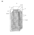
- FIG. 1 is an overall perspective view of a container 1 having an RFID module 5 according to an embodiment of the present invention.
- FIG. 2 is a developed view of the container 1 in FIG.
- the container 1 of the present embodiment includes a base material 3, an antenna pattern 7 formed on the first main surface 3s of the base material 3, and an RFID module 5 mounted on the antenna pattern 7.
- the container 1 is, for example, an assembly-type box formed into a three-dimensional shape by assembling a flat base material 3 as shown in FIG.
- the container 1 has a rectangular parallelepiped shape, for example, and the base material 3 is made of, for example, paper, resin, or plastic.
- the base material 3 includes a first surface 3a, a second surface 3b, a third surface 3c, a fourth surface 3d, a fifth surface 3e, a sixth surface 3f, and a first flap 3g, a second flap 3h, and a third flap. Equipped with 3k.
- the first surface 3a to the fourth surface 3d become a side surface when assembled
- the fifth surface 3e becomes an upper surface when assembled
- the sixth surface 3f becomes a lower surface when assembled.
- the first main surface 3s of the base material 3 is a surface to be the outer surface (front surface) of the container 1
- the second main surface 3t of the base material 3 is a surface to be the inner surface (back surface) of the container 1.
- the first main surface 3s of the first flap 3g is attached to the second main surface 3t of the second surface 3b via an adhesive layer (not shown) when assembled.
- the first main surface 3s of the second flap 3h is attached to the second main surface 3t of the first surface 3a via an adhesive layer when assembled.
- the first main surface 3s of the third flap 3k is attached to the second main surface 3t of the first surface 3a via an adhesive layer when assembled.
- the RFID module 5 of this embodiment is a wireless communication device configured to perform wireless communication (transmission / reception) with a high frequency signal having a communication frequency (carrier frequency).
- the RFID module 5 is configured to perform wireless communication with, for example, a high frequency signal having a frequency for communication in the UHF band.
- the UHF band is a frequency band from 860 MHz to 960 MHz.
- the antenna pattern 7 is formed on the first main surface 3s of the base material 3.
- the antenna pattern 7 has a first antenna film 7a and a second antenna film 7b.
- a gap 9 is formed between the first antenna film 7a and the second antenna film 7b.
- the antenna pattern 7 is made of a film body of a carbon-based material such as graphite or a conductive material such as tin or zinc-based material by printing.
- the thickness of the antenna pattern 7 is, for example, about 0.1 ⁇ m to 3 ⁇ m.
- the sheet resistance of the antenna pattern 7 of the embodiment is larger than the sheet resistance of the antenna pattern of the conventional dipole antenna.
- the sheet resistance of the antenna pattern 7 is large, the following problems that have not occurred in the conventional dipole antenna occur.
- the antenna pattern 7 of the conventional dipole antenna is formed of a metal foil such as aluminum, and its thickness is, for example, larger than 5 ⁇ m and 40 ⁇ m or less, and the sheet resistance of the antenna pattern 7 is 0.05 ⁇ / ⁇ or less.
- the thickness of the metal foil is, for example, 5 ⁇ m
- printing is performed on the metal pattern by decorative printing or gravure printing or offset printing as a design
- gravure printing is printed. Since the thickness is about 0.5 ⁇ m to 3 ⁇ m, printing misalignment (blurring or bleeding) occurs due to a large step due to the thickness of the metal film as the antenna foil. As a result, it has not been possible to print directly as a design on a container with an antenna pattern using metal leaf.
- the thickness of the metal film is about 0.1 ⁇ m to 3 ⁇ m. With this thickness, gravure printing can be performed on the printing electrode of the antenna pattern 7, and for example, printing can be performed so as to hide the antenna pattern 7 with white ink, which improves the design.
- the printed antenna pattern 7 has a small film thickness, so that the sheet resistance becomes large, for example, 0.5 ⁇ / ⁇ to 50 ⁇ /. ⁇ It will be about.
- the resistance value of the matching circuit section between the RFIC and the antenna will be the same thickness as the metal film, the resistance value of the matching circuit section will increase, the matching loss will increase, and the RFID module will not operate.
- an antenna pattern (antenna electrode) made of a thin metal film cannot generate electromagnetic wave radiation due to a (series) resonance phenomenon, but when an electromagnetic wave is received by the metal film, a current is applied so as to cancel the electromagnetic wave in the metal film. Flows and shields electromagnetic waves.
- This current is also called an eddy current. Since the current component flowing through the metal film due to the eddy current is not due to the resonance phenomenon of the antenna electrode, it can correspond to all frequency components regardless of the electrode pattern shape. This eddy current is known as an effect of the metal shield, but it is not usually used as an antenna.
- the RFID module 5 has a parallel resonant circuit RC1 as a filter circuit that transmits only a current having a unique resonant frequency to the RFIC 23, so that the eddy current is frequency-selected and the current flows through the RFIC 23 to generate energy. Be transmitted. Only a specific frequency is selected between the antenna pattern 7 as an antenna electrode and the RFID module 5, impedance matching is performed, and energy transfer between the RFID 23 and the antenna pattern 7 becomes possible. In this way, it is considered that communication with the RFIC 23 becomes possible.
- the state where the sheet resistance of the antenna pattern 7 is high occurs not only by the thickness of the antenna pattern 7 but also by the manufacturing method of the antenna pattern 7.
- the antenna pattern 7 is formed of a conductive paste such as Ag paste or a conductive polymer material
- the sheet resistance may be 0.5 ⁇ / ⁇ or more. Even in such a case, wireless communication can be performed with the container 1 of the present embodiment.
- FIG. 3 is a perspective plan view of the RFID module
- FIG. 4 is a sectional view taken along the line IV in FIG.
- FIG. 5 shows a plan view of a conductor pattern formed on the substrate of the RFID module
- FIG. 5a is a plan view of the conductor pattern formed on the upper surface of the substrate of the RFID module
- FIG. 5b is a plan view of the conductor pattern formed on the lower surface of the substrate. It is a perspective plan view seen from the top of the conductor pattern.
- FIG. 6 is a cross-sectional view of the arrowhead VI in FIG.
- the XYZ coordinate system facilitates the understanding of the invention and does not limit the invention.
- the X-axis direction indicates the longitudinal direction of the RFID module 5
- the Y-axis direction indicates the depth (width) direction
- the Z-axis direction indicates the thickness direction.
- the X, Y, and Z directions are orthogonal to each other.
- the RFID module 5 is attached to the upper surface of the antenna pattern 7 via an adhesive 15 such as double-sided tape or synthetic resin.
- the RFID module 5 includes a substrate 21 and an RFID 23 mounted on the substrate 21.
- the substrate 21 is a flexible substrate such as polyimide.
- a protective film 25 is formed on the upper surface of the substrate 21 on which the RFIC 23 is mounted.
- the protective film 25 is, for example, an elastomer such as polyurethane or a hot melt agent such as ethylene vinyl acetate (EVA).
- a protective film 27 is also attached to the lower surface of the substrate 21.
- the protective film 27 is, for example, a coverlay film such as a polyimide film (Kapton tape).
- a third electrode 33, a fourth electrode 35, a conductor pattern L1a of the main portion of the first inductance element L1 and a conductor pattern L2a of the main portion of the second inductance element L2 are formed on the upper surface of the substrate 21, a third electrode 33, a fourth electrode 35, a conductor pattern L1a of the main portion of the first inductance element L1 and a conductor pattern L2a of the main portion of the second inductance element L2 are formed.
- the third electrode 33 is connected to one end of the conductor pattern L1a
- the fourth electrode 35 is connected to one end of the conductor pattern L2a.
- These conductor patterns are, for example, a copper foil patterned by photolithography.
- the first electrode 29 and the second electrode 31 are capacitively coupled to the antenna pattern 7, respectively. Further, on the lower surface of the substrate 21, a part of the conductor pattern L1b of the first inductance element L1 and the conductor patterns L3a, L3b (conductor pattern surrounded by the alternate long and short dash line) and L3c of the third inductance element L3 are formed. These conductor patterns are also, for example, a copper foil patterned by photolithography.
- One end of a part of the conductor pattern L1b of the first inductance element L1 and one end of the conductor pattern L3a of the third inductance element L3 are connected to the first electrode 29.
- one end of the conductor pattern L2b of the second inductance element L2 and one end of the conductor pattern L3c of the third inductance element L3 are connected to the second electrode 31.
- a conductor pattern L3b is connected between the other end of the conductor pattern L3a of the third inductance element L3 and the other end of the conductor pattern L3c.
- the other end of the conductor pattern L1b of the first inductance element L1 and the other end of the conductor pattern L1a of the first inductance element L1 are connected via the via conductor V1.
- the other end of the conductor pattern L2b of the second inductance element L2 and the other end of the conductor pattern L2a of the second inductance element L2 are connected via the via conductor V2.
- the RFIC 23 is mounted on the third electrode 33 and the fourth electrode 35 formed on the upper surface of the substrate 21. That is, the terminal 23a of the RFIC 23 is connected to the third electrode 33, and the terminal 23b of the RFIC 23 is connected to the fourth electrode 35.
- the conductor patterns L3a of the first inductance element L1 and the third inductance element L3 are formed in different layers of the substrate 21, and are arranged so that their coil openings overlap each other.
- the conductor patterns L3c of the second inductance element L2 and the third inductance element L3 are formed in different layers of the substrate 21, and the coil openings are arranged so as to overlap each other.
- the RFIC 23 is positioned on the surface of the substrate 21 between the conductor pattern L3c of the second inductance element L2 and the third inductance element L3 and the conductor pattern L3a of the first inductance element L1 and the third inductance element L3. do.
- the conductor patterns L1a, L1b, and L3a form the first coil Cr1
- the conductor patterns L2a, L2b, and L3c form the second coil Cr2.
- a first current path CP1 passing through the upper surface and the lower surface of the substrate 21 and a second current path CP2 passing through the lower surface of the substrate 21 are formed.
- the first current path CP1 reaches the second electrode 31 from the first electrode 29 through the branch point N1, the conductor pattern L1b, the conductor pattern L1a, RFIC23, the conductor pattern L2a, the conductor pattern L2b, and the branch point N2.
- the second current path CP2 reaches the second electrode 31 from the first electrode 29 through the branch point N1, the conductor pattern L3a, the conductor pattern L3b, the conductor pattern L3c, and the branch point N2.
- first inductance element L1 composed of a conductor pattern L1b connected via a conductor pattern L1a and a via conductor V1, and a conductor pattern L2b connected via a conductor pattern L2a and a via conductor V2.
- the winding directions of the current flowing through the second inductance element L2 are opposite to each other, and the magnetic field generated by the first inductance element L1 and the magnetic field generated by the second inductance element L2 cancel each other out.
- the first current path CP1 and the second current path CP2 are formed in parallel with each other between the first electrode 29 and the second electrode 31, respectively.
- the dipole antenna when a dipole antenna type antenna pattern is provided in a container, the dipole antenna may be affected by the contents in the container and communication may be hindered. This is because the physical length of the antenna pattern is fixed, and if the electrical length of the antenna pattern is affected by the contents such as liquid and changes, communication may not be possible. Therefore, the dipole antenna is not suitable as an antenna formed directly on the container.
- the metal coating of the pouch 41 and the antenna pattern 7 are capacitively coupled.
- the dielectric constant of the RFID tag may change depending on the dielectric material such as the liquid to be stored, and the electric length of the antenna pattern 7 may be shorter than the physical length. Further, the change in the dielectric constant also changes depending on the distance between the content and the antenna pattern 7. Therefore, each time the position of the contents changes in the container, the communication characteristics also change.
- a high frequency signal is transmitted and received using the eddy current generated in the antenna pattern 7, and the RFID module 5 transmits a current due to an electromagnetic wave having a resonance frequency of the communication frequency.
- the RFID module 5 transmits a current due to an electromagnetic wave having a resonance frequency of the communication frequency.
- the antenna film 7b By printing away from the pouch 41, the antenna film 7b has almost no capacitive coupling, and the antenna film 7a selectively has a capacitive coupling with the metal coating surface.
- the antenna film 7a By printing away from the pouch 41, the antenna film 7b has almost no capacitive coupling, and the antenna film 7a selectively has a capacitive coupling with the metal coating surface.
- an eddy current flows through the antenna film 7a, an eddy current also flows through the metal coating surface due to capacitive coupling, so that the metal coating surface can also be used for transmitting and receiving high-frequency signals.
- the resonance frequency is fixed by the RFID module 5 instead of designing the frequency by the length of the antenna pattern 7. It is possible to cope with the frequency change due to the length of the antenna pattern 7.
- the RFIC 23 is a small chip, and each coil pattern is wound so that the first coil Cr1 and the second coil Cr2 having a laminated structure cancel the magnetic field.
- the periphery of the RFID module 23 is fixed by the dielectric constant of the RFID module 5 and is not affected by the dielectric (contents) contained in the container 1, so that the frequency matching with the RFID module 23 does not change.
- the permittivity of the substrate 21 between the conductor patterns L1a and L2a and the conductor patterns L3a and L3c is fixed, and there is no change between the line capacitances.
- the conductor patterns L1a and L2a and the conductor patterns L3a and L3c are covered with a protective film 25 and a protective film 27 as a protective layer having a fixed dielectric constant, respectively. In this way, the dielectric constant of the RFID module 5 is fixed.
- a figure eight coil is formed by the first coil Cr1 and the second coil Cr2 of the RFID module 5, and the magnetic field of the RFID module 5 is formed. Is a configuration that does not easily leak to the outside. Since the magnetic field of the RFID module 5 is less likely to leak, the inductance value is less likely to change due to external factors.
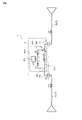
- FIG. 8 is an equivalent circuit diagram of the RFID module 5.
- the first current path CP1 is a part of the parallel resonant circuit RC1 which is an LC parallel resonant circuit, and matches the radio wave of the communication frequency. Therefore, the radio wave of the communication frequency is used as the antenna pattern 7. Is received, a current flows through the RFIC 23.
- the RFID module 5 is formed with a parallel resonant circuit RC1.
- the parallel resonant circuit RC1 is a loop circuit composed of a first inductance element L1, an RFIC23, a second inductance element L2, and a third inductance element L3.
- the capacitance C1 is composed of a first antenna film 7a, a first electrode 29, an adhesive 15, and a protective film 27.
- the capacitance C2 is composed of a second antenna film 7b, a second electrode 31, an adhesive 15, and a protective film 27.
- the fourth inductance element L4 is an inductance component of the first antenna film 7a of the antenna pattern 7
- the fifth inductance element L5 is an inductance component of the second antenna film 7b of the antenna pattern 7.
- the parallel resonance circuit RC1 is designed to perform LC parallel resonance by impedance matching with radio waves at the communication frequency. As a result, the RFID module is matched with the RFID in the communication frequency, and the communication distance of the RFID module 5 in the communication frequency can be secured.
- the antenna pattern 7 may be a part of the pattern 43 of the container 1.
- the pattern 43 may be a metal film or a resin film.
- FIG. 10 is a flowchart showing a flow of manufacturing the container of the present embodiment.
- the antenna pattern 7 is printed and formed on the first main surface 3s of the base material 3 of the container 1 before assembly.
- the antenna pattern 7 can be formed by gravure printing or offset printing. By using gravure printing or offset printing, the antenna pattern 7 can be printed at high speed.
- step S2 the pattern 43 is printed and formed on the first main surface 3s of the base material 3 of the container 1.
- the pattern 43 can be formed by gravure printing or offset printing, similarly to the antenna pattern 7. It should be noted that step S1 and step S2 may be performed separately, or may be performed simultaneously or continuously.
- step S1 and step S2 are performed in the same printing process, the pattern 43 and the antenna pattern 7 can be printed simultaneously or continuously on the container 1, so that the position of the antenna pattern 7 can be fixed to the container 1. It is possible to individually design the positional relationship between the contents and the antenna pattern 7. Further, by printing the entire surface of white or printing a pattern on the antenna film (7a, 7b), the antenna pattern 7 can be made difficult to see, and the design can be improved.
- step S3 the RFID module 5 is mounted on the antenna pattern 7.
- the RFID module 5 is mounted on the upper surface of the antenna pattern 7 via the adhesive 15.
- step S4 the container 1 is assembled. It should be noted that the container 1 can be shipped to the user in a state before being assembled. In this case, the user assembles the container 1 and stores the contents in the container 1.
- the container 1 of the present embodiment is the container 1 provided with the RFID module 5, and is formed on the insulating base material 3 forming the outer shape of the container 1 and the first main surface 3s of the base material 3.
- the antenna pattern 7 having the formed first antenna film 7a and the second antenna film 7b is provided.
- the RFID module 5 includes an RFIC 23, a parallel resonance circuit RC1 as a filter circuit for transmitting a current due to an electromagnetic wave having a unique resonance frequency which is a communication frequency to the RFIC 23, and a first electrode 29 and a second electrode connected to the parallel resonance circuit RC1. 31 and.
- the first electrode 29 of the RFID module 5 and the first antenna film 7a are electrically connected.
- the sheet resistance of each of the first antenna film 7a and the second antenna film 7b is 0.5 ⁇ / ⁇ or more.
- the antenna pattern 7 can be formed by printing, so that the pattern can be printed on the container 1 and the antenna pattern can be printed. It is also possible to perform printing with and at the same time, and it is possible to improve the manufacturing efficiency of the container 1 on which the pattern is printed. Further, since the antenna pattern 7 can be printed directly on the container 1, the degree of freedom in designing the shape of the antenna pattern 7 can be improved, and the RFID module 5 which suppresses the reduction of the design of the container 1 is provided. Container 1 can be provided. Further, since the antenna pattern 7 can be formed at high speed and in a large amount by printing, the container 1 provided with the RFID module 5 can be provided at a lower cost than in the conventional case.
- electromagnetic waves are radiated by causing series resonance with the antenna pattern of the high frequency of the communication frequency.
- both ends of the metal object and the antenna pattern are capacitively coupled, and a closed circuit is formed from the end of one antenna pattern to the end of the other antenna pattern via the metal object. It is formed, does not emit electromagnetic waves, and does not operate as an antenna.
- the dielectric constant around the antenna pattern will increase because there is a dielectric near the antenna pattern. This causes the wavelength to be shortened and the series resonance frequency to be lower than the initial setting of the antenna. Since the series resonance frequency changes depending on the distance between the antenna pattern and the dielectric and the ratio of the antenna pattern near the dielectric, the operation of the antenna becomes unstable depending on the contents in the conventional configuration in which the RFID tag is attached. Become.
- the antenna pattern 7 is formed on the base material 3 of the container 1, and the sheet resistances of the first antenna film 7a and the second antenna film 7b are 0.5 ⁇ / Since it is ⁇ or more, an eddy current is generated instead of the series resonance in the antenna pattern 7.
- the eddy current generated in the antenna pattern 7 is matched by the parallel resonant circuit RC1 of the RFID module 5 to supply electric power to the RFID module 23. Since the antenna pattern 7 can be printed anywhere on the surface of the container 1 and the frequency is not designed by the pattern length of the antenna, the degree of freedom of the pattern is high. As a result, the antenna pattern 7 can be made into an optimum pattern shape with respect to the shapes of the container 1 and the contents.
- the electromagnetic wave can be radiated from the antenna pattern 7.
- the container 1 provided with the RFID module 5 of the present embodiment does not utilize series resonance, wireless communication is possible even if a metal object or a dielectric is present around the antenna pattern in the container 1. be.
- the antenna pattern 7 is formed on the first main surface 3s of the base material 3 as a part of the pattern. In this way, since the antenna pattern 7 can be a part of the decorative printing, the design of the container 1 can be improved.
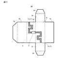
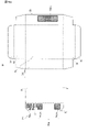
- FIG. 11 is a developed view of the container 1A in the first modification.
- the container 1A in the first modification has a configuration in which the antenna pattern 7 of the container 1 of the embodiment has a meander shape. In this way, the first antenna film 7a and the second antenna film 7b of the antenna pattern 7 may extend in a meander shape.
- Other configurations of the container 1A of the modification 1 are substantially the same as those of the container 1 of the embodiment. Even with such a configuration, the communication characteristics do not change, so that the container 1A of the modified example 1 can obtain the same effect as the container 1 of the embodiment.
- FIG. 12 is a developed view of the container 1B in the modified example 2.
- the container 1B in the second modification has a configuration in which the antenna pattern 7 of the container 1 of the embodiment is formed over two surfaces of the third surface 3c and the fourth surface 3d. Further, as in the modification 1, the antenna pattern 7 has a meander shape.
- Other configurations of the container 1B of the modification 2 are substantially the same as those of the container 1 of the embodiment. Even with such a configuration, the communication characteristics do not change, so that the container 1B of the modified example 2 can obtain the same effect as the container 1 of the embodiment.
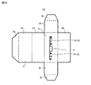
- FIG. 13 is a developed view of the container 1C in the modified example 3 of the embodiment.
- the container 1C in the modified example 3 of the embodiment has a shape in which the antenna pattern 7 includes the logotype in the container 1 of the embodiment.
- the “MURATA” logotype is formed as an antenna pattern, and the logotype functions as an antenna.
- the antenna pattern 7 may include a logo mark instead of the logotype, or may include a combination of the logotype and the logo mark. Even with such a configuration, the communication characteristics do not change, so that the container 1C of the modified example 3 can obtain the same effect as the container 1 of the embodiment.
- the pattern is a printed matter for decorating the container 1 formed on the first main surface 3s of the container 1, and includes, for example, a figure, a picture, a character, a logotype, a logo mark, and a combination thereof. ..
- FIG. 14A is a developed view of the container 1D in the modified example 4 of the embodiment.
- FIG. 14B is a partially enlarged view of a developed view of the container 1D.
- FIG. 15 is a perspective perspective view of the container 1D.
- 16 is a perspective view of the XVI arrow of FIG. 15, and is a perspective side view of the container 1D.
- FIG. 17 is a perspective view of XVII of FIG. 15 and is a perspective front view of the container 1D.
- the container 1D in the modified example 4 of the embodiment is a modified example of the container 1 shown in FIG. 7, and has a configuration in which the antenna pattern 7 in the container 1 of the embodiment is formed in the first flap 3 g.
- the base material 3 connects the first surface 3a and the second surface 3b having the first main surface 3s, which are the side surfaces of the box-shaped container 1D, and the first surface 3a and the second surface 3b by an adhesive layer. It has a first flap 3g continuous with the first surface 3a for the purpose.
- the first antenna film 7Da is formed on the first flap 3g so as to overlap the lid 51b
- the second antenna film 7Db is formed on the first flap 3g so as to overlap the container body 51a.
- the container 1D has flaps other than the first flap 3g to the third flap 3k for reinforcement, for example, to prevent dust from entering the inside of the assembled container 51.
- the antenna pattern 7D in the modified example 4 of the embodiment is an asymmetric dipole antenna.
- the antenna pattern 7D has a first antenna film 7Da having a meander-shaped pattern and a second antenna film 7Db longer than the first antenna film 7Da.
- the second antenna film 7Db has a meander-shaped pattern 7Dba and a linear-shaped pattern 7Dbb.
- the antenna pattern 7D is formed, for example, by stamping a vapor-deposited foil or printing a conductive paste.
- Container 1D further accommodates one or more containers 51 inside in a state of being assembled in a box.
- the container 51 has a container body 51a for accommodating a liquid such as water, and a lid 51b attached to the container body 51a and having a hollow inside.
- the container body 51a is made of, for example, metal or resin.
- the container body 51a may be a metal article itself.
- the lid 51b is made of resin, for example. Therefore, the lid 51b secures a space Sp in the container 1D between the container main body 51a and the fifth surface, which is the upper surface of the container 1D, with almost no liquid or metal.
- the antenna pattern 7D and the RFID module 5 are formed on the first flap 3g, the antenna pattern 7D and the RFID module 5 are visually hidden at the time of forming the box, and the container is formed. It does not affect the design of 1D. Further, since the RFID module 5 is sandwiched between the first flap 3g and the second surface 3b at the time of assembling the box, it does not come into contact with the container 51 which is the content. Therefore, there is no possibility that the RFID module 5 will fall out of the container 1D when the container 51 is taken in and out.
- the first antenna film 7Da which is one electrode of the antenna pattern 7D, is arranged away from the container body 51a for accommodating the liquid as the content or the container body 51a which is a metal, the liquid or metal. It is not easily affected by the contents of the product, and it is possible to suppress the reduction of communication characteristics.
- the container 51 does not have to have the lid 51b.
- the height of the container 1D is secured to such an extent that a space Sp is formed between the upper surface of the container 51 and the fifth surface 3e of the container 1D.
- the first antenna film 7Da is formed on the first flap 3g so as to overlap the space Sp between the upper surface of the container 51 and the fifth surface 3e of the container 1D.
- the first antenna film 7Da has a meander shape
- the second antenna film 7Eab has a meander shape instead. It may have a flat plate shape. Since the second antenna film 7Eab on the flat plate is arranged so as to overlap the contents of the container 1E in a side view when the box is assembled, the same effect as the above-mentioned effect can be obtained.
- the second antenna film 7Eab of the antenna pattern 7Ea formed on the first flap 3g may have various shapes other than the flat plate shape.
- 20A and 20B are shown as examples of the shape of the second antenna film.
- 20A (a) and 20B (b) and 20B (a) and 20B (b) are partially enlarged views of the developed view of the container in the modified example of the embodiment, respectively.
- the second antenna film 7Ebb of the antenna pattern 7Eb formed on the first flap 3g of the container 1Eb may have an uneven shape on the side surface side of the first flap 3g. ..
- the second antenna film 7Ebc of the antenna pattern 7Ec formed on the first flap 3g of the container 1Ec has a wave shape vibrating in the width direction of the first flap 3g. May be good.
- the second antenna film 7Ebd of the antenna pattern 7Ed formed on the first flap 3g of the container 1Ed may be formed by combining a plurality of annular conductor patterns.
- a plurality of conductor patterns may be formed in a mesh shape.
- the non-metal region of the first flap 3g can be increased as compared with the antenna pattern 7E, so that the region where the base material 3 of the first flap 3g is exposed and the second.
- the region where the base material 3 on the two surfaces 3b is exposed can be directly bonded by the adhesive layer 11. Thereby, the adhesive strength between the first flap 3g and the second surface can be improved.
- the first antenna film 7Da and the second antenna film 7Db having a meander shape have other meander shapes as shown in FIGS. 21A and 21B. May be good.
- 21A (a) and 21A (b) and FIGS. 21B (a) and 21B (b) are partially enlarged views of the developed view of the container in the modified example of the embodiment, respectively.
- the antenna pattern 7Fa of the container 1Fa has a meander-shaped first antenna film 7Faa and a second antenna film 7Fab longer than the first antenna film 7Faa.
- the second antenna film 7Fab has a meander-shaped pattern 7Faba and a linear-shaped pattern 7Fab.
- the first antenna film 7Faa and the pattern 7Faba are formed at both ends in the longitudinal direction of the first flap 3 g.
- the tips of the first antenna film 7Faa and the pattern 7Faba have the first flap 3g along the side 3aa between the first flap 3g and the first surface 3a, that is, the container 1Fa is assembled. In a state of being bent from the surface 3a, it extends so as to face the corner between the first flap 3g and the first surface 3a. Since the tips of the first antenna film 7Faa and the pattern 7Faba extend in the vicinity of the side side 3aa to be a crease, the respective tips of the antenna pattern 7Fa extend to the edge portion of the box-shaped container 1Fa. As a result, the contents are separated from the contents accommodated in the container 1F, so that the influence of the contents on the antenna pattern 7F can be reduced when the contents are a metal-coated pouch 41 or the like.
- the meander shape of the first antenna film 7Faa and the pattern 7Faba may have an amplitude of the meander shape formed in the width direction of the first flap 3g, and is shown in FIG. 21A (b).
- the amplitude of the meander shape may be formed in an oblique direction so that the pattern of the meander shape faces the angle between the first flap 3g and the first surface 3a from the middle.
- the antenna pattern 7Fb of the container 1Fb has a meander-shaped first antenna film 7Fba and a second antenna film 7Fbb longer than the first antenna film 7Fba.
- the second antenna film 7Fbb has a meander-shaped pattern 7Fbba and a linear-shaped pattern 7Fbbb.
- the first antenna film 7Fba and the pattern 7Fbba are formed at both ends in the longitudinal direction of the first flap 3g, and the respective tip portions extend in the vicinity of the side side 3aa to be a crease.
- the antenna pattern 7Fc of the container 1Fc has a first antenna film 7Fca having a meander shape and a second antenna film 7Fcb longer than the first antenna film 7Fca.
- the second antenna film 7Fcb has a meander-shaped pattern 7Fcba and a linear-shaped pattern 7Fcb.
- the first antenna film 7Fca and the pattern 7Fcba are formed at both ends in the longitudinal direction of the first flap 3g.
- the pattern 7 Fcba is formed along the extension direction of the side side 3aa where the amplitude direction of the meander shape is a crease, and even if the meander shape pattern is formed so as to extend toward the edge 3ga at the tip of the first flap 3g. good.
- the content is, for example, a metal object such as a PTP (Press Through Pack) sheet.
- PTP Pressure Through Pack
- FIG. 22 shows an example in which the first antenna film of the antenna pattern formed on the first flap 3g does not have a meander shape.
- 22 (a), 22 (b), and 22 (c) are partially enlarged views of the developed view of the container in the modified example of the embodiment, respectively.
- the antenna pattern 7Ga has a loop-shaped first antenna film 7Gaa and a second antenna film 7Gab longer than the first antenna film 7Gaa.
- the second antenna film 7Gab has a rectangular shape.
- One end of the first antenna film 7Gaa is a land 7Gak to which one end of the RFID module 5 is attached, and a pattern is formed from the outside to the inside in a spiral shape from the land 7Gak.
- the electric field is strong in the region Ds between the portion 7Gad on the first surface 3a side of the first antenna film 7Gaa facing the land 7Gak and the land 7Gak. Therefore, the pattern of the loop-shaped first antenna film 7Gaa is formed so as to wind inward, for example, clockwise so that the region Ds does not overlap the contents contained in the container 1Ga.
- the antenna pattern 7Gb of the container 1Gb has a first antenna film 7Gaa and a rectangular second antenna film 7Gab.
- the second antenna film 7Gab is formed with one or more holes 7gbe. Since the base material 3 is exposed in the holes 7 gbe, the adhesive layer 11 can improve the adhesive force between the first flap 3 g and the second surface 3b.
- the antenna pattern 7Gc of the container 1Gc has a first antenna film 7Gaa and a rectangular second antenna film 7Gac.
- the second antenna film 7Gac is arranged close to the side side 3aa which is a crease. That is, the distance Dv between the second antenna film 7Gac and the margin 3ga is longer than the distance Dw between the second antenna film 7Gac and the side 3aa. As a result, the region where the second antenna film 7Gac overlaps with the contents contained in the container 1Gc can be reduced.
- FIG. 23 is a partially enlarged view of a developed view of the container 1H in the modified example 5 of the embodiment
- FIG. 23A is a diagram showing an antenna pattern formed on the first flap 3g
- FIG. 23B is a diagram showing the antenna pattern formed on the first flap 3g.
- It is a peripheral view of RFIC23
- FIG. 23C is a diagram showing an antenna pattern to which RFIC23 is attached.
- the container 1H in the modification 5 of the embodiment is a modification of the container 1D shown in FIG. 14A.
- an inductor is formed on the antenna pattern side and the RFID 23 is attached to the antenna pattern which also has the function of an inductor. It is a configuration to attach.
- the antenna pattern 7H in the modified example 5 of the embodiment is an asymmetric dipole antenna.
- the antenna pattern 7H has a first antenna film 7Ha that also has a function as an inductor, and a second antenna film 7Hb.
- the first antenna film 7Ha has a land 7Haa electrically connected to the other terminal of the RFIC 23 and a loop pattern 7Hab extending in a loop from the land 7Haa to the land 7Hbc.
- the first antenna film 7Ha functions as a matching circuit, impedance-matches the first antenna film 7Ha and the RFIC 23, and enables energy transfer between the RFIC 23 and the antenna pattern 7H.
- the second antenna film 7Hb has a land 7Hbc electrically connected to one terminal of the RFIC 23, a pattern 7Hbb linearly extending from the land 7Hbc, and an antenna film 7Hba having a meander-shaped pattern.
- the first and second antenna films 7Ha and 7Hb are formed, for example, by stamping a vapor-deposited foil or printing a conductive paste.
- the RFIC 23 includes electrodes 63 and 64 connected to the two terminals 23a and 23b of the RFIC 23, respectively, and a resin sheet 65 on which the electrodes 63 and 64 are formed. It is attached to the land 7Haa and the land 7Hbc via the.
- the electrodes 63 and 64 and the lands 7Haa and the lands 7Hbc are arranged so as to overlap each other, and the electrodes 63 and 64 and the lands 7Haa and the lands 7Hbc are capacitively coupled, respectively.
- the first antenna film 7Ha that also functions as an inductor is formed on the first flap 3g, so that the antenna pattern 7H and the RFIC 23 are formed at the time of box formation. Is hidden in appearance and does not affect the design of the container 1H.
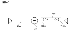
- FIG. 24A is a developed view of the container 1K in the modified example 6 of the embodiment
- FIG. 24B is a diagram showing an antenna pattern formed on the first flap 3g
- FIG. 23B is a peripheral view of the RFIC 23
- FIG. 23 (c) is a diagram showing an antenna pattern to which the RFIC 23 is attached.
- the container 1K in the modification 5 of the embodiment is a modification of the container 1D shown in FIG. 14A.
- the second antenna film 7Kb is divided into a plurality of electrodes, and the container 1K functions as one antenna pattern in an assembled state. It is a configuration to do.
- the antenna pattern 7K has a first antenna film 7Da and a second antenna film 7Kb.
- the second antenna film 7Kb was arranged on the first main surface 3s side of the first flap 3g, the first pattern electrode 7Kba and the second pattern electrode 7Kbb arranged on the first main surface 3s side, and the second surface 3b on the first main surface 3s side.
- a third pattern electrode 7Kbc is provided.
- the first pattern electrode 7Kba to the third pattern electrode 7Kbc are formed by, for example, stamping a vapor-deposited foil or printing a conductive paste, respectively.
- the second surface 3b is arranged between the first pattern electrode 7Kba and the second pattern electrode 7Kbb and the third pattern electrode 7Kbc.
- a capacitance C3 is generated between the first pattern electrode 7Kba and the third pattern electrode 7Kbc
- a capacitance C4 is generated between the second pattern electrode 7Kbb and the third pattern electrode 7Kbc, and the capacitances are coupled to each other.
- the first pattern electrode 7Kba to the third pattern electrode 7Kbc function as one antenna pattern.
- a first antenna film 7Da, a first pattern electrode 7Kba and a second pattern electrode 7Kbb of the second antenna film 7Kb are formed on the back surface (second main surface 3t) side of the second surface 3b.
- the RFID module 5 may be arranged, and the third pattern electrode 7Kbc may be arranged on the front surface (first main surface 3s) side of the first flap 3g. Even with this configuration, when the container 1L is assembled, the first pattern electrode 7Kba to the third pattern electrode 7Kbc can function as one antenna pattern. Further, the first pattern electrode 7Kba to the third pattern electrode 7Kbc may be arranged on either the front surface or the back surface of the base material 3.
- the container 1 is an assembly type, but the present invention is not limited to this.
- the container 1 may be a bottle or a PET bottle.
- the antenna pattern 7 is a part of the pattern formed on the container 1, but the present invention is not limited to this.
- a printing film may be further applied to the container 1 on which the antenna pattern 7 is formed to give a design different from that of the antenna pattern 7.
- the communication frequency band is the UHF band, but the frequency band is not limited to this. It may be configured to perform wireless communication with a high frequency signal having a frequency (carrier frequency) for communication in the HF band.
- the HF band is a frequency band of 13 MHz or more and 15 MHz or less.
- the antenna pattern 7 may be formed on the second main surface 3t instead of the first main surface 3S of the base material 3. That is, the antenna pattern 7 may be formed inside the container 1.
Landscapes
- Engineering & Computer Science (AREA)
- Computer Hardware Design (AREA)
- Microelectronics & Electronic Packaging (AREA)
- Physics & Mathematics (AREA)
- General Physics & Mathematics (AREA)
- Theoretical Computer Science (AREA)
- Computer Networks & Wireless Communication (AREA)
- Mechanical Engineering (AREA)
- Details Of Aerials (AREA)
- Cartons (AREA)
- Details Of Rigid Or Semi-Rigid Containers (AREA)
- Aerials With Secondary Devices (AREA)
- Support Of Aerials (AREA)
Priority Applications (2)
| Application Number | Priority Date | Filing Date | Title |
|---|---|---|---|
| JP2022549685A JP7243931B2 (ja) | 2020-11-30 | 2021-11-17 | Rfidモジュールを備えた容器及びrfidモジュールを備えた容器の製造方法 |
| US18/301,592 US12327155B2 (en) | 2020-11-30 | 2023-04-17 | Container provided with RFID module and method for manufacturing container provided with RFID module |
Applications Claiming Priority (6)
| Application Number | Priority Date | Filing Date | Title |
|---|---|---|---|
| JP2020-198748 | 2020-11-30 | ||
| JP2020198748 | 2020-11-30 | ||
| JP2021081611 | 2021-05-13 | ||
| JP2021-081611 | 2021-05-13 | ||
| JP2021-105801 | 2021-06-25 | ||
| JP2021105801 | 2021-06-25 |
Related Child Applications (1)
| Application Number | Title | Priority Date | Filing Date |
|---|---|---|---|
| US18/301,592 Continuation US12327155B2 (en) | 2020-11-30 | 2023-04-17 | Container provided with RFID module and method for manufacturing container provided with RFID module |
Publications (1)
| Publication Number | Publication Date |
|---|---|
| WO2022113851A1 true WO2022113851A1 (ja) | 2022-06-02 |
Family
ID=81754591
Family Applications (1)
| Application Number | Title | Priority Date | Filing Date |
|---|---|---|---|
| PCT/JP2021/042274 Ceased WO2022113851A1 (ja) | 2020-11-30 | 2021-11-17 | Rfidモジュールを備えた容器及びrfidモジュールを備えた容器の製造方法 |
Country Status (3)
| Country | Link |
|---|---|
| US (1) | US12327155B2 (https=) |
| JP (1) | JP7243931B2 (https=) |
| WO (1) | WO2022113851A1 (https=) |
Cited By (1)
| Publication number | Priority date | Publication date | Assignee | Title |
|---|---|---|---|---|
| WO2025083959A1 (ja) * | 2023-10-18 | 2025-04-24 | 学校法人金沢工業大学 | レクテナ装置及びそれに用いるアンテナ回路 |
Families Citing this family (2)
| Publication number | Priority date | Publication date | Assignee | Title |
|---|---|---|---|---|
| WO2018235714A1 (ja) * | 2017-06-19 | 2018-12-27 | 株式会社村田製作所 | コイル素体集合体およびコイルモジュールとその製造方法 |
| USD1044756S1 (en) * | 2021-07-20 | 2024-10-01 | Crestron Electronics, Inc. | RFID reader |
Citations (6)
| Publication number | Priority date | Publication date | Assignee | Title |
|---|---|---|---|---|
| JP2002049905A (ja) * | 2000-08-03 | 2002-02-15 | Dainippon Printing Co Ltd | 非接触データキャリア付きパッケージと製品情報管理方法 |
| JP2002259934A (ja) * | 2001-03-06 | 2002-09-13 | Dainippon Printing Co Ltd | Rfidタグ付き液体容器 |
| US20100090832A1 (en) * | 2006-08-31 | 2010-04-15 | Francois Bozet | Method of protecting a radio frequency identification inlay |
| WO2010146944A1 (ja) * | 2009-06-19 | 2010-12-23 | 株式会社村田製作所 | 無線icデバイス及び給電回路と放射板との結合方法 |
| EP2428457A1 (fr) * | 2010-09-09 | 2012-03-14 | Centre Technique de l'Industrie des Papiers, Cartons et Celluloses | Feuille d'emballage avec système d'identification radiofréquence et etui d'emballage constitué d'une telle feuille d'emballage |
| WO2019039484A1 (ja) * | 2017-08-24 | 2019-02-28 | 株式会社村田製作所 | Rfidタグ付きパッケージ |
Family Cites Families (6)
| Publication number | Priority date | Publication date | Assignee | Title |
|---|---|---|---|---|
| CN101948025B (zh) * | 2006-02-22 | 2012-05-30 | 东洋制罐株式会社 | 带rfid标签的金属盖及使用其的金属物品 |
| JP5028176B2 (ja) * | 2007-07-25 | 2012-09-19 | 株式会社日立製作所 | Rfidタグ実装パッケージおよびその製造方法 |
| WO2013085076A1 (en) * | 2011-12-09 | 2013-06-13 | Ricoh Company, Ltd. | Rfid tag, rfid system, and package including rfid tag |
| US8666090B1 (en) * | 2013-02-26 | 2014-03-04 | Full Code Audio LLC | Microphone modeling system and method |
| US20170154197A1 (en) * | 2015-11-26 | 2017-06-01 | Chung-Ping Lai | RFIG tag, security system, and method of protecting products using the same |
| WO2020137060A1 (ja) * | 2018-12-25 | 2020-07-02 | 株式会社村田製作所 | 無線通信デバイス |
-
2021
- 2021-11-17 JP JP2022549685A patent/JP7243931B2/ja active Active
- 2021-11-17 WO PCT/JP2021/042274 patent/WO2022113851A1/ja not_active Ceased
-
2023
- 2023-04-17 US US18/301,592 patent/US12327155B2/en active Active
Patent Citations (6)
| Publication number | Priority date | Publication date | Assignee | Title |
|---|---|---|---|---|
| JP2002049905A (ja) * | 2000-08-03 | 2002-02-15 | Dainippon Printing Co Ltd | 非接触データキャリア付きパッケージと製品情報管理方法 |
| JP2002259934A (ja) * | 2001-03-06 | 2002-09-13 | Dainippon Printing Co Ltd | Rfidタグ付き液体容器 |
| US20100090832A1 (en) * | 2006-08-31 | 2010-04-15 | Francois Bozet | Method of protecting a radio frequency identification inlay |
| WO2010146944A1 (ja) * | 2009-06-19 | 2010-12-23 | 株式会社村田製作所 | 無線icデバイス及び給電回路と放射板との結合方法 |
| EP2428457A1 (fr) * | 2010-09-09 | 2012-03-14 | Centre Technique de l'Industrie des Papiers, Cartons et Celluloses | Feuille d'emballage avec système d'identification radiofréquence et etui d'emballage constitué d'une telle feuille d'emballage |
| WO2019039484A1 (ja) * | 2017-08-24 | 2019-02-28 | 株式会社村田製作所 | Rfidタグ付きパッケージ |
Cited By (1)
| Publication number | Priority date | Publication date | Assignee | Title |
|---|---|---|---|---|
| WO2025083959A1 (ja) * | 2023-10-18 | 2025-04-24 | 学校法人金沢工業大学 | レクテナ装置及びそれに用いるアンテナ回路 |
Also Published As
| Publication number | Publication date |
|---|---|
| US20230259735A1 (en) | 2023-08-17 |
| US12327155B2 (en) | 2025-06-10 |
| JPWO2022113851A1 (https=) | 2022-06-02 |
| JP7243931B2 (ja) | 2023-03-22 |
Similar Documents
| Publication | Publication Date | Title |
|---|---|---|
| US12327155B2 (en) | Container provided with RFID module and method for manufacturing container provided with RFID module | |
| EP2166618B1 (en) | Radio ic device and component for radio ic device | |
| US8662403B2 (en) | Wireless IC device and component for wireless IC device | |
| JP7074275B1 (ja) | Rfidモジュールを備えた容器 | |
| JP6575698B2 (ja) | Rfidタグ、それを備えた物品、およびrfidタグの製造方法 | |
| JP5510560B2 (ja) | 無線通信デバイス | |
| JP6583589B2 (ja) | 無線通信デバイス | |
| US10476147B2 (en) | Antenna device and method of manufacturing the same | |
| JP2021522572A (ja) | Rfidタグ設計を備えた遮蔽rfidストラップの使用方法 | |
| JP2011193245A (ja) | アンテナ装置、無線通信デバイス及び無線通信端末 | |
| JP6785966B2 (ja) | Rfidタグ付きパッケージ | |
| JP7294562B2 (ja) | Rfidモジュールを備えた容器 | |
| JP7239073B2 (ja) | Rfidモジュールを備えた容器 | |
| US20230359847A1 (en) | Container including rfid module | |
| JP7201137B2 (ja) | Rfidモジュールを備えた容器 |
Legal Events
| Date | Code | Title | Description |
|---|---|---|---|
| 121 | Ep: the epo has been informed by wipo that ep was designated in this application |
Ref document number: 21897825 Country of ref document: EP Kind code of ref document: A1 |
|
| ENP | Entry into the national phase |
Ref document number: 2022549685 Country of ref document: JP Kind code of ref document: A |
|
| NENP | Non-entry into the national phase |
Ref country code: DE |
|
| 122 | Ep: pct application non-entry in european phase |
Ref document number: 21897825 Country of ref document: EP Kind code of ref document: A1 |