WO2022102770A1 - 磁化回転素子、磁気抵抗効果素子及び磁気メモリ - Google Patents
磁化回転素子、磁気抵抗効果素子及び磁気メモリ Download PDFInfo
- Publication number
- WO2022102770A1 WO2022102770A1 PCT/JP2021/041886 JP2021041886W WO2022102770A1 WO 2022102770 A1 WO2022102770 A1 WO 2022102770A1 JP 2021041886 W JP2021041886 W JP 2021041886W WO 2022102770 A1 WO2022102770 A1 WO 2022102770A1
- Authority
- WO
- WIPO (PCT)
- Prior art keywords
- layer
- spin
- linear expansion
- orbit torque
- coefficient
- Prior art date
- Legal status (The legal status is an assumption and is not a legal conclusion. Google has not performed a legal analysis and makes no representation as to the accuracy of the status listed.)
- Ceased
Links
Images


Classifications
-
- H—ELECTRICITY
- H10—SEMICONDUCTOR DEVICES; ELECTRIC SOLID-STATE DEVICES NOT OTHERWISE PROVIDED FOR
- H10N—ELECTRIC SOLID-STATE DEVICES NOT OTHERWISE PROVIDED FOR
- H10N50/00—Galvanomagnetic devices
- H10N50/10—Magnetoresistive devices
-
- H—ELECTRICITY
- H10—SEMICONDUCTOR DEVICES; ELECTRIC SOLID-STATE DEVICES NOT OTHERWISE PROVIDED FOR
- H10N—ELECTRIC SOLID-STATE DEVICES NOT OTHERWISE PROVIDED FOR
- H10N52/00—Hall-effect devices
- H10N52/80—Constructional details
- H10N52/85—Materials of the active region
-
- H—ELECTRICITY
- H10—SEMICONDUCTOR DEVICES; ELECTRIC SOLID-STATE DEVICES NOT OTHERWISE PROVIDED FOR
- H10B—ELECTRONIC MEMORY DEVICES
- H10B61/00—Magnetic memory devices, e.g. magnetoresistive RAM [MRAM] devices
- H10B61/20—Magnetic memory devices, e.g. magnetoresistive RAM [MRAM] devices comprising components having three or more electrodes, e.g. transistors
-
- H—ELECTRICITY
- H10—SEMICONDUCTOR DEVICES; ELECTRIC SOLID-STATE DEVICES NOT OTHERWISE PROVIDED FOR
- H10B—ELECTRONIC MEMORY DEVICES
- H10B61/00—Magnetic memory devices, e.g. magnetoresistive RAM [MRAM] devices
- H10B61/20—Magnetic memory devices, e.g. magnetoresistive RAM [MRAM] devices comprising components having three or more electrodes, e.g. transistors
- H10B61/22—Magnetic memory devices, e.g. magnetoresistive RAM [MRAM] devices comprising components having three or more electrodes, e.g. transistors of the field-effect transistor [FET] type
-
- H—ELECTRICITY
- H10—SEMICONDUCTOR DEVICES; ELECTRIC SOLID-STATE DEVICES NOT OTHERWISE PROVIDED FOR
- H10D—INORGANIC ELECTRIC SEMICONDUCTOR DEVICES
- H10D48/00—Individual devices not covered by groups H10D1/00 - H10D44/00
- H10D48/40—Devices controlled by magnetic fields
-
- H—ELECTRICITY
- H10—SEMICONDUCTOR DEVICES; ELECTRIC SOLID-STATE DEVICES NOT OTHERWISE PROVIDED FOR
- H10N—ELECTRIC SOLID-STATE DEVICES NOT OTHERWISE PROVIDED FOR
- H10N50/00—Galvanomagnetic devices
- H10N50/80—Constructional details
- H10N50/85—Materials of the active region
Definitions
- the present invention relates to a magnetization rotating element, a magnetoresistive effect element, and a magnetic memory.
- Giant magnetoresistive (GMR) elements consisting of a multilayer film of a ferromagnetic layer and a non-magnetic layer, and tunnel magnetoresistive (TMR) elements using an insulating layer (tunnel barrier layer, barrier layer) as the non-magnetic layer are magnetic resistance.
- TMR tunnel magnetoresistive
- insulating layer tunnel barrier layer, barrier layer
- Magnetoresistive elements can be applied to magnetic sensors, high frequency components, magnetic heads and non-volatile random access memory (MRAM).
- MRAM is a storage element in which a magnetoresistive element is integrated.
- the MRAM reads and writes data by utilizing the characteristic that the resistance of the magnetoresistive sensor changes when the direction of mutual magnetization of the two ferromagnetic layers sandwiching the non-magnetic layer in the magnetoresistive sensor changes.
- the direction of magnetization of the ferromagnetic layer is controlled by using, for example, a magnetic field generated by an electric current. Further, for example, the direction of magnetization of the ferromagnetic layer is controlled by utilizing the spin transfer torque (STT) generated by passing a current in the stacking direction of the magnetoresistive effect element.
- STT spin transfer torque
- SOT spin-orbit torque
- Patent Document 1 describes that in a magnetoresistive effect element using spin-orbit torque, magnetization reversal of a ferromagnetic layer becomes easy by using spin-orbit torque wiring as a laminated film and increasing the number of laminated interfaces.
- Spin-orbit torque wiring tends to generate heat by applying a write current.
- thermal stress is applied to the spin-orbit torque wiring.
- the spin-orbit torque wiring is composed of a plurality of layers, the spin-orbit torque wiring may be distorted due to the difference in the expansion rate of each layer. The strain causes cracks and peeling between layers of the laminated film.
- the present invention has been made in view of the above circumstances, and an object of the present invention is to provide a magnetized rotation element, a magnetoresistive effect element, and a magnetic memory capable of suppressing deterioration of spin-orbit torque wiring due to strain.
- the present invention provides the following means for solving the above problems.
- the magnetizing rotating element includes a spin-orbit torque wiring and a first ferromagnetic layer in contact with the spin-orbit torque wiring, and the spin-orbit torque wiring is the first ferromagnetic layer. It has a first layer, a second layer, and a third layer in order from the side closest to the above, and the linear expansion coefficient of the material constituting the second layer is the linear expansion of the material constituting the first layer. It is between the coefficient and the linear expansion coefficient of the material constituting the third layer.
- the first layer contains a first element as a main element
- the second layer contains a second element different from the first element as a main element
- the first layer is described.
- the third layer contains the first element and a third element different from the second element as main elements, and the linear expansion coefficient of the second element is the linear expansion coefficient of the first element and the linear expansion of the third element. It may be between the elements.
- the first layer contains a first element as a main element
- the second layer contains a second element different from the first element as a main element
- the first layer is described.
- the third layer contains the first element and a third element different from the second element as the main elements, and the first element and the third element are Au, Bi, Hf, Ir, Mo, Pd, Pt, Rh. , Ru, Ta, W, Ag, Al, Cu, Ge, Si, and the second element is Ag, Au, Bi, Co, Cr, Cu, Fe, Ge, Hf, Ir, It may be any one of Mo, Ni, Pd, Pt, Rh, Ru and Ta.
- the first element is any one of Au, Bi, Hf, Ir, Mo, Pd, Pt, Rh, Ru, Ta, and W
- the second element is any one of Ag, Au, Bi, Co, Cr, Cu, Fe, Ge, Hf, Ir, Mo, Ni, Pd, Pt, Rh, Ru, and Ta
- the third element is It may be any one of Ag, Al, Cu, Ge and Si.
- the peripheral length of the first layer is shorter than the peripheral lengths of the second layer and the third layer, and the peripheral length of the second layer is the peripheral length of the third layer. It may be shorter than the perimeter.
- the peripheral length of the first layer is longer than the peripheral lengths of the second layer and the third layer, and the peripheral length of the second layer is the peripheral length of the third layer. It may be longer than the perimeter.
- the magnetization rotating element according to the above aspect may further include a fourth layer containing the same material as the second layer, and a fifth layer containing the same material as the first layer or the third layer. ..
- the fourth layer is between the fifth layer and the third layer.
- the film thickness of the second layer may be thinner than the film thickness of the first layer and the third layer.
- the second layer may be a continuous film having a plurality of openings or a layer including a plurality of components scattered in an island shape.
- the magnetization rotating element according to the above aspect further includes an intermediate layer in contact with the spin orbit torque wiring and a conductive layer connected to the spin orbit torque wiring via the intermediate layer, and the intermediate layer is provided.
- the coefficient of linear expansion of the constituent material may be between the coefficient of linear expansion of the layer in contact with the intermediate layer and the coefficient of linear expansion of the conductive layer.
- the magnetic resistance effect element according to the second aspect is the magnetized rotating element according to the above aspect, a non-magnetic layer in contact with the first ferromagnetic layer of the magnetized rotating element, and the first ferromagnetic layer. A second ferromagnetic layer with a non-magnetic layer sandwiched between them is provided.
- the magnetic memory according to the third aspect includes a plurality of the above-mentioned magnetoresistive elements.
- the magnetization rotating element, magnetoresistive effect element, and magnetic memory according to the present invention can suppress deterioration of spin-orbit torque wiring due to strain.
- the x direction is, for example, a direction from the first conductive layer 31 to the second conductive layer 32.
- the z direction is a direction orthogonal to the x direction and the y direction.
- the z direction is an example of the stacking direction in which each layer is laminated.
- the + z direction may be expressed as “up” and the ⁇ z direction may be expressed as “down”.
- the top and bottom do not always match the direction in which gravity is applied.
- connection means that, for example, the dimension in the x direction is larger than the smallest dimension among the dimensions in the x direction, the y direction, and the z direction. The same applies when extending in other directions.
- connection is not limited to the case of being physically connected. For example, not only when two layers are physically in contact with each other, but also when two layers are connected by sandwiching another layer between them is included in "connection".
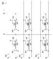
- FIG. 1 is a block diagram of the magnetic array 200 according to the first embodiment.
- the magnetic array 200 includes a plurality of magnetoresistive elements 100, a plurality of write wiring WLs, a plurality of common wiring CLs, a plurality of read wiring RLs, a plurality of first switching elements Sw1, and a plurality of second switching elements. It includes Sw2 and a plurality of third switching elements Sw3.
- the magnetic array 200 can be used for, for example, a magnetic memory.
- Each write wiring WL electrically connects the power supply and one or more magnetoresistive elements 100.
- the common wiring CL is wiring used both when writing data and when reading data, respectively.
- Each of the common wiring CLs electrically connects the reference potential and one or more magnetoresistive elements 100.
- the reference potential is, for example, ground.
- the common wiring CL may be provided in each of the plurality of magnetoresistive elements 100, or may be provided across the plurality of magnetoresistive elements 100.
- the readout wiring RL electrically connects the power supply and one or more magnetoresistive elements 100, respectively.
- the power supply is connected to the magnetic array 200 during use.
- Each magnetoresistive element 100 is connected to the first switching element Sw1, the second switching element Sw2, and the third switching element Sw3, respectively.
- the first switching element Sw1 is connected between the magnetoresistive effect element 100 and the write wiring WL.
- the second switching element Sw2 is connected between the magnetoresistive effect element 100 and the common wiring CL.
- the third switching element Sw3 is connected to the read wiring RL extending over the plurality of magnetoresistive element 100.
- a write current flows between the write wiring WL connected to the predetermined magnetoresistive effect element 100 and the common wiring CL.
- the write current flows, data is written to the predetermined magnetoresistive element 100.
- the second switching element Sw2 and the third switching element Sw3 are turned on, a read current flows between the common wiring CL connected to the predetermined magnetoresistive element 100 and the read wiring RL.
- the read current flows, data is read from the predetermined magnetoresistive element 100.
- the first switching element Sw1, the second switching element Sw2, and the third switching element Sw3 are elements that control the flow of current.
- the first switching element Sw1, the second switching element Sw2, and the third switching element Sw3 are, for example, a transistor, an element utilizing a phase change of a crystal layer such as an Ovonic Threshold Switch (OTS), and a metal insulator transition.
- An element such as a (MIT) switch that utilizes a change in band structure, an element that utilizes a breakdown voltage such as a Zener diode and an avalanche diode, and an element whose conductivity changes as the atomic position changes.
- the magnetoresistive effect element 100 connected to the same wiring shares the third switching element Sw3.
- the third switching element Sw3 may be provided in each magnetoresistive element 100. Further, a third switching element Sw3 may be provided in each magnetoresistive element 100, and the first switching element Sw1 or the second switching element Sw2 may be shared by the magnetoresistive element 100 connected to the same wiring.
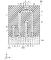
- FIG. 2 is a cross-sectional view of a characteristic portion of the magnetic array 200 according to the first embodiment.
- FIG. 2 is a cross section of the magnetoresistive element 100 cut along the xz plane passing through the center of the width in the y direction of the spin-orbit torque wiring 20 described later.
- the first switching element Sw1 and the second switching element Sw2 shown in FIG. 2 are transistor Trs.
- the third switching element Sw3 is electrically connected to the read wiring RL and is located, for example, in the y direction of FIG.
- the transistor Tr is, for example, a field effect transistor, and has a gate electrode G, a gate insulating film GI, a source S formed on the substrate Sub, and a drain D.
- the substrate Sub is, for example, a semiconductor substrate.
- the transistor Tr and the magnetoresistive sensor 100 are electrically connected via the via wiring V, the first conductive layer 31 and the second conductive layer 32. Further, the transistor Tr and the write wiring WL or the common wiring CL are connected by a via wiring V.
- the via wiring V extends in the z direction, for example.
- the read wiring RL is connected to the laminated body 10 via the electrode E.
- the via wiring V, the electrode E, the first conductive layer 31 and the second conductive layer 32 include a material having conductivity.
- the periphery of the magnetoresistive effect element 100 and the transistor Tr is covered with an insulating layer In.
- the insulating layer In is an insulating layer that insulates between the wirings of the multilayer wiring and between the elements.
- the insulating layer In may be, for example, silicon oxide (SiO x ), silicon nitride (SiN x ), silicon carbide (SiC), chromium nitride, silicon carbide (SiCN), silicon oxynitride (SiON), aluminum oxide (Al 2 O). 3 ), zirconium oxide (ZrO x ), magnesium oxide (MgO), aluminum nitride (AlN) and the like.
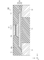
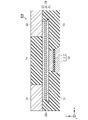
- FIG. 3 is a cross-sectional view of the magnetoresistive effect element 100.
- FIG. 3 is a cross section of the magnetoresistive element 100 cut in the xz plane passing through the center of the width of the spin-orbit torque wiring 20 in the y direction.
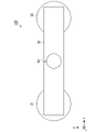
- FIG. 4 is a plan view of the magnetoresistive effect element 100 as viewed from the z direction.
- the magnetoresistive element 100 includes, for example, a laminate 10, a spin-orbit torque wiring 20, a first conductive layer 31, and a second conductive layer 32.
- the laminate 10 is electrically in contact with the spin-orbit torque wiring 20.
- the laminate 10 is physically in contact with, for example, the spin-orbit torque wiring 20.
- the laminated body 10 is laminated on or above the spin-orbit torque wiring 20, for example. Another layer may be provided between the laminate 10 and the spin-orbit torque wiring 20.
- the first conductive layer 31 and the second conductive layer 32 are connected to the spin-orbit torque wiring 20.
- Another layer may be provided between each of the first conductive layer 31 and the second conductive layer 32 and the spin-orbit torque wiring 20.
- the first conductive layer 31 and the second conductive layer 32 are located at positions sandwiching the laminated body 10 when viewed from the z direction.
- the resistance value of the laminated body 10 in the z direction changes when spin is injected into the laminated body 10 from the spin track torque wiring 20.
- the magnetoresistive effect element 100 is a magnetic element using spin orbit torque (SOT), and may be referred to as a spin orbit torque type magnetoresistive element, a spin injection type magnetoresistive element, or a spin current magnetic resistance effect element. ..
- the laminated body 10 is sandwiched between the spin-orbit torque wiring 20 and the electrode E (see FIG. 2) in the z direction.
- the laminated body 10 is a columnar body.
- the plan view shape of the laminated body 10 from the z direction is, for example, a circle, an ellipse, or a quadrangle.
- the side surface 10s of the laminated body 10 is inclined with respect to the z direction, for example.
- the laminated body 10 has, for example, a first ferromagnetic layer 1, a second ferromagnetic layer 2, and a non-magnetic layer 3.
- the first ferromagnetic layer 1 is in contact with, for example, the spin-orbit torque wiring 20, and is laminated on the spin-orbit torque wiring 20.
- Spin is injected into the first ferromagnetic layer 1 from the spin-orbit torque wiring 20.
- the magnetization of the first ferromagnetic layer 1 receives spin-orbit torque (SOT) due to the injected spin, and the orientation direction changes.
- the second ferromagnetic layer 2 is in the z direction of the first ferromagnetic layer 1.
- the first ferromagnetic layer 1 and the second ferromagnetic layer 2 sandwich the non-magnetic layer 3 in the z direction.
- the first ferromagnetic layer 1 and the second ferromagnetic layer 2 each have magnetization.
- the magnetization of the second ferromagnetic layer 2 is less likely to change in the orientation direction than the magnetization of the first ferromagnetic layer 1 when a predetermined external force is applied.
- the first ferromagnetic layer 1 is sometimes referred to as a magnetization free layer
- the second ferromagnetic layer 2 is sometimes referred to as a magnetization fixed layer or a magnetization reference layer.
- the magnetization fixing layer is on the side away from the substrate Sub, and is called a top pin structure.
- the resistance value of the laminated body 10 changes according to the difference in the relative angles of magnetization between the first ferromagnetic layer 1 and the second ferromagnetic layer 2 sandwiching the non-magnetic layer 3.
- the first ferromagnetic layer 1 and the second ferromagnetic layer 2 include a ferromagnet.
- the ferromagnetic material is, for example, a metal selected from the group consisting of Cr, Mn, Co, Fe and Ni, an alloy containing one or more of these metals, and at least one of these metals and B, C, and N. It is an alloy containing the element of.
- the ferromagnetic material is, for example, Co—Fe, Co—Fe—B, Ni—Fe, Co—Ho alloy, Sm—Fe alloy, Fe—Pt alloy, Co—Pt alloy, CoCrPt alloy.
- the first ferromagnetic layer 1 and the second ferromagnetic layer 2 may contain a Whistler alloy.
- Whisler alloys include intermetallic compounds with a chemical composition of XYZ or X2YZ .
- X is a transition metal element or noble metal element of Group Co, Fe, Ni, or Cu on the periodic table
- Y is a transition metal of Group Mn, V, Cr, or Ti, or an elemental species of X
- Z is Group III. It is a typical element of Group V.
- the Whisler alloy is, for example, Co 2 FeSi, Co 2 FeGe, Co 2 FeGa, Co 2 MnSi, Co 2 Mn 1-a Fe a Al b Si 1-b , Co 2 FeGe 1-c Ga c and the like. Whisler alloys have a high spin polarizability.
- the non-magnetic layer 3 contains a non-magnetic material.
- the non-magnetic layer 3 is an insulator (when it is a tunnel barrier layer), for example, Al 2 O 3 , SiO 2 , MgO, MgAl 2 O 4 and the like can be used as the material thereof.
- a material or the like in which a part of Al, Si, and Mg is replaced with Zn, Be, or the like can also be used.
- MgO and MgAl2O4 are materials that can realize a coherent tunnel, so that spin can be efficiently injected.
- the non-magnetic layer 3 is a metal, Cu, Au, Ag or the like can be used as the material.
- the non-magnetic layer 3 is a semiconductor, Si, Ge, CuInSe 2 , CuGaSe 2 , Cu (In, Ga) Se 2 and the like can be used as the material.
- the laminated body 10 may have a layer other than the first ferromagnetic layer 1, the second ferromagnetic layer 2, and the non-magnetic layer 3.
- a base layer may be provided between the spin-orbit torque wiring 20 and the first ferromagnetic layer 1.
- the base layer enhances the crystallinity of each layer constituting the laminated body 10.
- the cap layer may be provided on the uppermost surface of the laminated body 10.
- the laminated body 10 may have a ferromagnetic layer on the surface of the second ferromagnetic layer 2 opposite to the non-magnetic layer 3 via a spacer layer.
- the second ferromagnetic layer 2, the spacer layer, and the ferromagnetic layer have a synthetic antiferromagnetic structure (SAF structure).
- the synthetic antiferromagnetic structure consists of two magnetic layers sandwiching the non-magnetic layer.
- the antiferromagnetic coupling between the second ferromagnetic layer 2 and the ferromagnetic layer increases the coercive force of the second ferromagnetic layer 2 as compared with the case without the ferromagnetic layer.
- the ferromagnetic layer is, for example, IrMn, PtMn or the like.
- the spacer layer contains, for example, at least one selected from the group consisting of Ru, Ir, Rh.
- the spin-orbit torque wiring 20 has a length in the x direction longer than the y direction when viewed from the z direction, and extends in the x direction.
- the write current flows in the x direction of the spin-orbit torque wiring 20.
- At least a part of the spin-orbit torque wiring 20 sandwiches the first ferromagnetic layer 1 together with the non-magnetic layer 3 in the z direction.
- the spin-orbit torque wiring 20 generates a spin current by the spin Hall effect when the current I flows, and injects spin into the first ferromagnetic layer 1.
- the spin-orbit torque wiring 20 gives, for example, a spin-orbit torque (SOT) sufficient to reverse the magnetization of the first ferromagnetic layer 1 to the magnetization of the first ferromagnetic layer 1.
- SOT spin-orbit torque
- the spin Hall effect is a phenomenon in which a spin current is induced in a direction orthogonal to the direction in which a current flows, based on the spin-orbit interaction when a current is passed.
- the spin Hall effect is common to the normal Hall effect in that the moving (moving) charge (electron) can bend the moving (moving) direction.
- the first spin oriented in the ⁇ y direction is bent in the + z direction
- the second spin oriented in the + y direction is bent in the ⁇ z direction.
- the number of electrons in the first spin and the number of electrons in the second spin generated by the spin Hall effect are equal. That is, the number of electrons in the first spin in the + z direction is equal to the number of electrons in the second spin in the ⁇ z direction.
- the first spin and the second spin flow in the direction of eliminating the uneven distribution of spins. In the movement of the first spin and the second spin in the z direction, the charge flows cancel each other out, so that the amount of current becomes zero. Spin currents without current are especially called pure spin currents.
- the electron flow of the first spin is J ⁇
- the electron flow of the second spin is J ⁇
- the spin current JS occurs in the z direction.
- the first spin is injected into the first ferromagnetic layer 1 from the spin-orbit torque wiring 20.
- the spin-orbit torque wiring 20 has a first layer 21, a second layer 22, and a third layer 23 in order from the side closer to the first ferromagnetic layer 1.
- the second layer 22 is between the first layer 21 and the third layer 23.
- the first layer 21 is closer to the first ferromagnetic layer 1 than the third layer 23.
- the first layer 21, the second layer 22, and the third layer 23 have different materials or compositions.
- the coefficient of linear expansion of the material constituting the second layer 22 is between the coefficient of linear expansion of the material constituting the first layer 21 and the coefficient of linear expansion of the material constituting the third layer 23.
- the coefficient of linear expansion of the material constituting the second layer 22 is larger than the coefficient of linear expansion of the material constituting the first layer 21, and smaller than the coefficient of linear expansion of the material constituting the third layer 23.
- the difference between the linear expansion coefficient of the material constituting the third layer 23 and the linear expansion coefficient of the material constituting the second layer 22 is the linear expansion coefficient of the material constituting the third layer 23 and the first layer 21.
- the difference between the linear expansion coefficients of the constituent materials is preferably 70% or less, and the difference between the linear expansion coefficients of the materials constituting the second layer 22 and the linear expansion coefficients of the materials constituting the first layer 21 is the third. It is preferably 70% or less of the difference between the linear expansion coefficient of the material constituting the layer 23 and the linear expansion coefficient of the material constituting the first layer 21. Further, for example, the linear expansion coefficient of the material constituting the second layer 22 is smaller than the linear expansion coefficient of the material constituting the first layer 21, and is larger than the linear expansion coefficient of the material constituting the third layer 23.
- the difference between the linear expansion coefficient of the material constituting the first layer 21 and the linear expansion coefficient of the material constituting the second layer 22 is the linear expansion coefficient of the material constituting the first layer 21 and the third layer 23.
- the difference between the linear expansion coefficients of the constituent materials is preferably 70% or less, and the difference between the linear expansion coefficients of the materials constituting the second layer 22 and the linear expansion coefficients of the materials constituting the third layer 23 is the first. It is preferably 70% or less of the difference between the linear expansion coefficient of the material constituting the layer 21 and the linear expansion coefficient of the material constituting the third layer 23.
- ⁇ is the coefficient of linear expansion
- ⁇ T is the temperature change
- ⁇ L is the amount of change in length
- L is the length.
- the coefficient of linear expansion is a coefficient of linear expansion in the operating temperature range
- the length L as a reference for calculation is the length in the operating temperature range.
- the operating temperature range is the temperature at which the magnetoresistive sensor 100 is most frequently used, and is usually 25 ° C. when driven at room temperature. Since the coefficient of linear expansion does not have a thickness parameter, it can be obtained by forming a film thick enough to measure the material constituting each layer under the same conditions as each layer and evaluating the formed film.
- the coefficient of linear expansion of the main element may be regarded as the coefficient of linear expansion of each layer.
- the main element is the element having the highest composition ratio among the elements constituting each layer.
- the linear expansion coefficient of the main element can be regarded as an approximate linear expansion coefficient of each layer.
- the table below shows the coefficient of linear expansion of some elements.
- the linear expansion coefficient of the second element when the first layer 21 contains the first element as the main element, the second layer contains the second element as the main element, and the third layer contains the third element as the main element, the linear expansion coefficient of the second element. Is preferably between the linear expansion coefficient of the first element and the linear expansion coefficient of the third element.
- the coefficient of linear expansion of the second element is preferably larger than the coefficient of linear expansion of the first element and smaller than the coefficient of linear expansion of the third element.
- the difference between the linear expansion coefficient of the third element and the linear expansion coefficient of the second element is preferably 70% or less of the difference between the linear expansion coefficient of the third element and the linear expansion coefficient of the first element.
- the difference between the linear expansion coefficient of the two elements and the linear expansion coefficient of the first element is preferably 70% or less of the difference between the linear expansion coefficient of the third element and the linear expansion coefficient of the first element.
- the linear expansion coefficient of the second element is smaller than the linear expansion coefficient of the first element and larger than the linear expansion coefficient of the third element.
- the difference between the linear expansion coefficient of the first element and the linear expansion coefficient of the second element is preferably 70% or less of the difference between the linear expansion coefficient of the first element and the linear expansion coefficient of the third element.
- the difference between the linear expansion coefficient of the two elements and the linear expansion coefficient of the third element is preferably 70% or less of the difference between the linear expansion coefficient of the first element and the linear expansion coefficient of the third element.
- the first layer 21 contains, for example, any one or more of Au, Bi, Hf, Ir, Mo, Pd, Pt, Rh, Ru, Ta, W, Ag, Al, Cu, Ge, and Si.
- the main element (first element) of the first layer 21 is, for example, one of these elements.
- the first layer 21 may be a simple substance metal, an alloy, an intermetallic compound, or a nitride.
- the first layer 21 is closer to the first ferromagnetic layer 1 than the second layer 22 and the third layer 23, and the spin generated in the first layer 21 is diffused to reach the first ferromagnetic layer 1. It's hard to do. Therefore, the first layer 21 is preferably a material capable of injecting a large amount of spin into the first ferromagnetic layer 1.
- Non-magnetic heavy metals have stronger spin-orbit interaction than other metals. Therefore, it is preferable that the first layer 21 contains a heavy metal of a non-magnetic layer.
- Heavy metal means a metal having a specific density of yttrium (Y) or higher.
- the non-magnetic heavy metal is, for example, a non-magnetic metal having a d-electron or an f-electron in the outermost shell and having an atomic number of 39 or more and a large atomic number.
- the first layer 21 includes, for example, any one or more of Au, Bi, Hf, Ir, Mo, Pd, Pt, Rh, Ru, Ta, and W.
- the main element (first element) of the first layer 21 is preferably, for example, any of these elements.
- the second layer 22 contains, for example, any one or more of Ag, Au, Bi, Co, Cr, Cu, Fe, Ge, Hf, Ir, Mo, Ni, Pd, Pt, Rh, Ru, and Ta.
- the main element (second element) of the second layer 22 is, for example, one of these elements.
- the second layer 22 may be a simple substance metal, an alloy, an intermetallic compound, or a nitride.
- the third layer 23 contains, for example, any one or more of Au, Bi, Hf, Ir, Mo, Pd, Pt, Rh, Ru, Ta, W, Ag, Al, Cu, Ge, and Si.
- the main element (third element) of the third layer 23 is, for example, one of these elements.
- the third layer 23 may be a simple substance metal, an alloy, an intermetallic compound, or a nitride.
- the third layer 23 is farther from the first ferromagnetic layer 1 as compared with the first layer 21 and the second layer 22, and a part of the spin generated in the third layer 23 is in the first ferromagnetic layer 1. It is spread all the way. Therefore, it is preferable that the third layer 23 has a function other than the function of generating a large number of spins.
- the third layer 23 preferably contains a light metal.
- the third layer 23 contains, for example, any one or more of Ag, Al, Cu, Ge, and Si.
- the main element (third element) of the third layer 23 is preferably, for example, one of these elements.
- the first element, the second element, and the third element are not arbitrarily selected from the above elements, and the linear expansion coefficient of the second element is the linear expansion coefficient of the first element and the linear expansion coefficient of the third element. It is selected to be between and.
- Examples thereof include a combination in which the second element is Ta and the third element is Cu, the first element is W, the second element is Hf, and the third element is Cu.
- the side surface 20s of the spin-orbit torque wiring 20 is inclined with respect to the z direction, for example. Therefore, the perimeter of the first layer 21 is shorter than the perimeter of the second layer 22 and the third layer 23, and the perimeter of the second layer 22 is shorter than the perimeter of the third layer 23.
- the perimeter is the perimeter of the upper surface far from the substrate Sub of each layer.
- the linear expansion coefficient of each layer satisfies the relationship of "linear expansion coefficient of the third layer 23"> “linear expansion coefficient of the second layer 22"> “linear expansion coefficient of the first layer 21"
- the linear expansion coefficient of each layer The difference between can be reduced.
- the film thickness of the second layer 22 is thinner than, for example, the film thickness of the first layer 21 and the third layer 23. It is possible to suppress the spin generated in the third layer 23 from being diffused in the second layer 22.
- the film thickness of the first layer 21 is thicker than, for example, the film thickness of the third layer. Since the first layer 21 is in contact with the first ferromagnetic layer 1, the thicker the layer, the higher the spin injection efficiency into the first ferromagnetic layer 1.
- Each layer constituting the spin-orbit torque wiring 20 may also contain a magnetic metal or a topological insulator.
- a topological insulator is a substance in which the inside of the substance is an insulator or a high resistance substance, but a metallic state in which spin polarization occurs on the surface thereof.
- Each of the first conductive layer 31 and the second conductive layer 32 is an example of the conductive layer.
- Each of the first conductive layer 31 and the second conductive layer 32 is made of a material having excellent conductivity.
- the first conductive layer 31 and the second conductive layer 32 are, for example, Al, Cu, W, and Cr.
- the magnetoresistive sensor 100 is formed by a laminating step of each layer and a processing step of processing a part of each layer into a predetermined shape.
- a sputtering method, a chemical vapor deposition (CVD) method, an electron beam vapor deposition method (EB vapor deposition method), an atomic laser deposit method, or the like can be used for the lamination of each layer.
- CVD chemical vapor deposition
- EB vapor deposition method electron beam vapor deposition method
- atomic laser deposit method or the like.
- the processing of each layer can be performed by using photolithography or the like.
- impurities are doped at a predetermined position on the substrate Sub to form a source S and a drain D.
- a gate insulating film GI and a gate electrode G are formed between the source S and the drain D.
- the source S, drain D, gate insulating film GI, and gate electrode G serve as a transistor Tr.
- the insulating layer In is formed so as to cover the transistor Tr. Further, by forming an opening in the insulating layer In and filling the opening with a conductor, the via wiring V, the first conductive layer 31 and the second conductive layer 32 are formed.
- the write wiring WL and the common wiring CL are formed by laminating the insulating layer In to a predetermined thickness, forming a groove in the insulating layer In, and filling the groove with a conductor.
- the metal layer, the ferromagnetic layer, the non-magnetic layer, the ferromagnetic layer, and the hard mask layer are laminated in order on one surface of the insulating layer In, the first conductive layer 31 and the second conductive layer 32.
- the hard mask layer is processed into a predetermined shape.
- the predetermined shape is, for example, the outer shape of the spin-orbit torque wiring 20.
- the metal layer, the ferromagnetic layer, the non-magnetic layer, and the ferromagnetic layer are processed into a predetermined shape at once via the hard mask layer.
- the metal layer is processed into a predetermined shape to form a spin-orbit torque wiring 20.
- the hard mask layer has the outer shape of the laminated body 10.
- the unnecessary portion in the x direction of the laminate formed on the spin-orbit torque wiring 20 is removed via the hard mask layer.
- the laminated body 10 is processed into a predetermined shape to become the laminated body 10.
- the hard mask layer serves as an electrode E.
- the periphery of the laminated body 10 and the spin-orbit torque wiring 20 is filled with the insulating layer In to obtain the magnetoresistive element 100.
- the linear expansion coefficient of the material constituting the second layer 22 is the linear expansion coefficient of the material constituting the first layer 21 and the linear expansion coefficient of the material constituting the third layer 23.
- the thermal stress generated in the spin track torque wiring 20 can be relaxed.
- the magnetoresistive effect element 100 can suppress the generation of peeling and cracks between layers due to the heat generated during writing, and can prevent the spin-orbit torque wiring 20 from deteriorating.
- magnetoresistive sensor 100 Although an example of the magnetoresistive sensor 100 according to the first embodiment has been shown above, it is possible to add, omit, replace, and otherwise change the configuration within a range that does not deviate from the gist of the present invention.
- FIG. 5 is a cross-sectional view of the magnetoresistive effect element 101 according to the first modification.
- FIG. 5 is an xz cross section passing through the center of the spin-orbit torque wiring 26 in the y direction.
- the same components as those in FIG. 3 are designated by the same reference numerals, and the description thereof will be omitted.
- the spin-orbit torque wiring 26 has a first layer 21, a second layer 22, a third layer 23, a fourth layer 24, and a fifth layer 25.
- the fourth layer 24 is between the third layer 23 and the fifth layer 25.
- FIG. 5 an example in which the fourth layer 24 and the fifth layer 25 are each one layer is shown, but each may have a plurality of layers.
- the 4th layer 24 and the 5th layer 25 are alternately laminated in the order of the 4th layer 24 and the 5th layer 25 from the side closer to the 3rd layer 23.
- the fourth layer 24 contains the same material as the second layer 22.
- the fourth layer 24 is made of, for example, the same material as the second layer 22.
- the fifth layer 25 contains the same material as the first layer 21 or the third layer 23.
- the fifth layer 25 is made of, for example, the same material as the first layer 21 or the third layer 23.
- the magnetoresistive sensor 101 according to the first modification has the same effect as the magnetoresistive element 100 according to the first embodiment. Further, as the number of layers constituting the spin-orbit torque wiring 25 increases, the current is distributed to each layer, so that the amount of current flowing through each layer becomes smaller. Therefore, heat generation in each layer can be suppressed, and the generation of thermal stress can be suppressed. Further, by increasing the number of interfaces of different substances in the spin-orbit torque wiring 25, the Rashba effect is amplified and the magnetization reversal efficiency of the first ferromagnetic layer 1 can be increased.
- FIG. 6 is a cross-sectional view of the magnetoresistive effect element 102 according to the second modification.
- FIG. 6 is an xz cross section passing through the center of the spin-orbit torque wiring 27 in the y direction.
- the same components as those in FIG. 3 are designated by the same reference numerals, and the description thereof will be omitted.
- the spin-orbit torque wiring 27 has a first layer 21, a second layer 22A, and a third layer 23.
- the second layer 22A according to the first embodiment is not a uniform continuous film but a continuous film having a plurality of openings or a layer including a plurality of components scattered in an island shape. Is different.
- the second layer 22A shown in FIG. 7 is an example of a continuous membrane having a plurality of open APs.
- the second layer 22A shown in FIG. 8 is an example of a layer including a plurality of component ELs scattered in an island shape. If the film thickness of the second layer 22A is thin, it may not be a uniform continuous film.
- the material of the first layer 21 or the third layer 23 is filled between the opening AP and the component EL.
- the magnetoresistive effect element 102 according to the second modification can obtain the same effect as the magnetoresistive effect element 100 according to the first embodiment. Further, the stress generated in the in-plane direction between the opening AP and the component EL is relaxed. As a result, deterioration of the spin-orbit torque wiring 26 can be prevented.
- FIG. 9 is a cross-sectional view of the magnetoresistive effect element 103 according to the third modification.
- FIG. 9 is an xz cross section passing through the center of the spin-orbit torque wiring 20 in the y direction.
- the same components as those in FIG. 3 are designated by the same reference numerals, and the description thereof will be omitted.
- the magnetoresistive sensor 103 is different from the magnetoresistive element 100 according to the first embodiment in that it has an intermediate layer 40.
- the intermediate layer 40 is located between the first conductive layer 31 and the spin-orbit torque wiring 20 and between the second conductive layer 32 and the spin-orbit torque wiring 20.
- the intermediate layer 40 may be located only between the first conductive layer 31 and the spin-orbit torque wiring 20 and between the second conductive layer 32 and the spin-orbit torque wiring 20.
- the coefficient of linear expansion of the material constituting the intermediate layer 40 is, for example, between the coefficient of linear expansion of the third layer 23 and the first conductive layer 31 or the second conductive layer 32.
- the linear expansion coefficient of the material constituting the fourth layer 40 is, for example, the linear expansion coefficient of the first layer 21 and the first conductive layer 31 or the second conductive layer 32. Is between.
- the magnetoresistive sensor 103 according to the third modification has the same effect as the magnetoresistive element 100 according to the first embodiment. Further, the intermediate layer 40 can alleviate the thermal stress difference between the first conductive layer 31 or the second conductive layer 32 and the spin-orbit torque wiring 20, and can suppress peeling and the like at these interfaces.
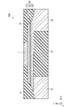
- FIG. 10 is a cross-sectional view of the magnetoresistive effect element 104 according to the fourth modification.
- FIG. 10 is an xz cross section passing through the center of the spin-orbit torque wiring 28 in the y direction.
- the same components as those in FIG. 3 are designated by the same reference numerals, and the description thereof will be omitted.
- the laminate 10 shown in FIG. 10 has a bottom pin structure in which the magnetization fixing layer (second ferromagnetic layer 2) is near the substrate Sub.
- the spin-orbit torque wiring 28 is laminated in the order of the first layer 21, the second layer 22, and the third layer 23 in order from the side closer to the substrate Sub.
- the spin-orbit torque wiring 28 is, for example, on the laminated body 10.
- the side surface 28s of the spin-orbit torque wiring 28 is inclined with respect to the z direction, for example. Therefore, the perimeter of the first layer 21 is longer than the perimeter of the second layer 22 and the third layer 23, and the perimeter of the second layer 22 is longer than the perimeter of the third layer 23. In this case, the length of the first layer 21 in the x direction is longer than the length of the third layer 23 in the x direction. Therefore, when the linear expansion coefficient of each layer satisfies the relationship of "linear expansion coefficient of the first layer 21"> "linear expansion coefficient of the second layer 22"> "linear expansion coefficient of the third layer 23", the line of each layer is satisfied. The difference in expansion coefficient can be reduced.
- the magnetoresistive sensor 104 according to the fourth modification is different only in the positional relationship of each configuration, and the same effect as the magnetoresistive element 100 according to the first embodiment can be obtained. Further, since the side wall 28s is inclined with respect to the z direction, the surface area of the spin-orbit torque wiring 28 is increased, and the heat dissipation is improved.
- FIG. 11 is a cross-sectional view of the magnetization rotating element 105 according to the second embodiment.
- the magnetization rotating element 105 is replaced with the magnetoresistive effect element 100 according to the first embodiment.
- the magnetizing rotating element 105 incidents light on the first ferromagnetic layer 1 and evaluates the light reflected by the first ferromagnetic layer 1.
- the magnetization rotating element 105 can be used, for example, as an optical element such as an image display device that utilizes a difference in the deflection state of light.
- the magnetization rotating element 105 can be used alone as an anisotropic magnetic sensor, an optical element utilizing the magnetic Faraday effect, and the like.
- the spin-orbit torque wiring 20 of the magnetizing rotating element 105 has a first layer 21, a second layer 22, and a third layer 23.
- the magnetoresistive element 100 according to the first embodiment is used. A similar effect can be obtained.
Landscapes
- Hall/Mr Elements (AREA)
Abstract
Description
図1は、第1実施形態にかかる磁気アレイ200の構成図である。磁気アレイ200は、複数の磁気抵抗効果素子100と、複数の書き込み配線WLと、複数の共通配線CLと、複数の読出し配線RLと、複数の第1スイッチング素子Sw1と、複数の第2スイッチング素子Sw2と、複数の第3スイッチング素子Sw3と、を備える。磁気アレイ200は、例えば、磁気メモリ等に利用できる。

図11は、第2実施形態に係る磁化回転素子105の断面図である。図1において、磁化回転素子105は、第1実施形態に係る磁気抵抗効果素子100と置き換えられる。
Claims (12)
- スピン軌道トルク配線と、
前記スピン軌道トルク配線上に接する第1強磁性層と、を備え、
前記スピン軌道トルク配線は、前記第1強磁性層に近い側から順に、第1層と、第2層と、第3層と、を有し、
前記第2層を構成する材料の線膨張係数は、前記第1層を構成する材料の線膨張係数と前記第3層を構成する材料の線膨張係数との間である、磁化回転素子。 - 前記第1層は、主元素として第1元素を含み、
前記第2層は、主元素として前記第1元素と異なる第2元素を含み、
前記第3層は、主元素として前記第1元素及び前記第2元素と異なる第3元素を含み、
前記第2元素の線膨張係数は、前記第1元素の線膨張係数と前記第3元素の線膨張係数との間である、請求項1に記載の磁化回転素子。 - 前記第1層は、主元素として第1元素を含み、
前記第2層は、主元素として前記第1元素と異なる第2元素を含み、
前記第3層は、主元素として前記第1元素及び前記第2元素と異なる第3元素を含み、
前記第1元素及び前記第3元素は、Au、Bi、Hf、Ir、Mo、Pd、Pt、Rh、Ru、Ta、W、Ag、Al、Cu、Ge、Siのいずれか一つであり、
前記第2元素は、Ag、Au、Bi、Co、Cr、Cu、Fe、Ge、Hf、Ir、Mo、Ni、Pd、Pt、Rh、Ru、Taのいずれか一つである、請求項1又は2に記載の磁化回転素子。 - 前記第1元素は、Au、Bi、Hf、Ir、Mo、Pd、Pt、Rh、Ru、Ta、Wのいずれか一つであり、
前記第2元素は、Ag、Au、Bi、Co、Cr、Cu、Fe、Ge、Hf、Ir、Mo、Ni、Pd、Pt、Rh、Ru、Taのいずれか一つであり、
前記第3元素は、Ag、Al、Cu、Ge、Siのいずれか一つである、請求項3に記載の磁化回転素子。 - 前記第1層の周囲長は、前記第2層及び前記第3層の周囲長より短く、
前記第2層の周囲長は、前記第3層の周囲長より短い、請求項1~4のいずれか一項に記載の磁化回転素子。 - 前記第1層の周囲長は、前記第2層及び前記第3層の周囲長より長く、
前記第2層の周囲長は、前記第3層の周囲長より長い、請求項1~4のいずれか一項に記載の磁化回転素子。 - 前記第2層と同じ材料を含む第4層と、
前記第1層又は第3層と同じ材料を含む第5層と、をさらに備え、
前記第4層は、前記第5層と前記第3層との間にある、請求項1~6に記載の磁化回転素子。 - 前記第2層の膜厚は、前記第1層及び前記第3層の膜厚より薄い、請求項1~7のいずれか一項に記載の磁化回転素子。
- 前記第2層は、複数の開口を有する連続膜又は島状に点在する複数の構成要素を含む層である、請求項1~8のいずれか一項に記載の磁化回転素子。
- 前記スピン軌道トルク配線に接する中間層と、前記中間層を介して前記スピン軌道トルク配線と接続される導電層と、をさらに備え、
前記中間層を構成する材料の線膨張係数は、前記中間層に接する層の線膨張係数と前記導電層の線膨張係数との間である、請求項1~9のいずれか一項に記載の磁化回転素子。 - 請求項1~10のいずれか一項に記載の磁化回転素子と、
前記磁化回転素子の前記第1強磁性層に接する非磁性層と、
前記第1強磁性層と共に前記非磁性層を間に挟む第2強磁性層と、を備える、磁気抵抗効果素子。 - 請求項11に記載の磁気抵抗効果素子を複数備える、磁気メモリ。
Priority Applications (2)
| Application Number | Priority Date | Filing Date | Title |
|---|---|---|---|
| CN202180038493.6A CN115700065B (zh) | 2020-11-16 | 2021-11-15 | 磁化旋转元件、磁阻效应元件和磁存储器 |
| US17/927,469 US12464959B2 (en) | 2020-11-16 | 2021-11-15 | Magnetization rotational element, magnetoresistive effect element, and magnetic memory |
Applications Claiming Priority (2)
| Application Number | Priority Date | Filing Date | Title |
|---|---|---|---|
| PCT/JP2020/042602 WO2022102122A1 (ja) | 2020-11-16 | 2020-11-16 | 磁化回転素子、磁気抵抗効果素子及び磁気メモリ |
| JPPCT/JP2020/042602 | 2020-11-16 |
Publications (1)
| Publication Number | Publication Date |
|---|---|
| WO2022102770A1 true WO2022102770A1 (ja) | 2022-05-19 |
Family
ID=81601349
Family Applications (2)
| Application Number | Title | Priority Date | Filing Date |
|---|---|---|---|
| PCT/JP2020/042602 Ceased WO2022102122A1 (ja) | 2020-11-16 | 2020-11-16 | 磁化回転素子、磁気抵抗効果素子及び磁気メモリ |
| PCT/JP2021/041886 Ceased WO2022102770A1 (ja) | 2020-11-16 | 2021-11-15 | 磁化回転素子、磁気抵抗効果素子及び磁気メモリ |
Family Applications Before (1)
| Application Number | Title | Priority Date | Filing Date |
|---|---|---|---|
| PCT/JP2020/042602 Ceased WO2022102122A1 (ja) | 2020-11-16 | 2020-11-16 | 磁化回転素子、磁気抵抗効果素子及び磁気メモリ |
Country Status (3)
| Country | Link |
|---|---|
| US (1) | US12464959B2 (ja) |
| CN (1) | CN115700065B (ja) |
| WO (2) | WO2022102122A1 (ja) |
Families Citing this family (1)
| Publication number | Priority date | Publication date | Assignee | Title |
|---|---|---|---|---|
| CN120936236A (zh) * | 2025-10-14 | 2025-11-11 | 中电海康集团有限公司 | 磁性隧道结器件及磁存储器 |
Citations (5)
| Publication number | Priority date | Publication date | Assignee | Title |
|---|---|---|---|---|
| WO2010134378A1 (ja) * | 2009-05-19 | 2010-11-25 | 富士電機ホールディングス株式会社 | 磁気メモリ素子およびそれを用いる記憶装置 |
| JP2017059594A (ja) * | 2015-09-14 | 2017-03-23 | 株式会社東芝 | 磁気メモリ |
| WO2019045055A1 (ja) * | 2017-09-04 | 2019-03-07 | Tdk株式会社 | スピン軌道トルク型磁化反転素子及び磁気メモリ |
| JP2019057553A (ja) * | 2017-09-20 | 2019-04-11 | 株式会社東芝 | 磁気記憶装置 |
| JP2019068086A (ja) * | 2017-02-27 | 2019-04-25 | Tdk株式会社 | スピン流磁化回転素子、磁気抵抗効果素子及び磁気メモリ |
Family Cites Families (11)
| Publication number | Priority date | Publication date | Assignee | Title |
|---|---|---|---|---|
| JP2007096032A (ja) * | 2005-09-29 | 2007-04-12 | Toyota Industries Corp | 絶縁基板及び半導体装置並びに絶縁基板の製造方法 |
| FR2963153B1 (fr) | 2010-07-26 | 2013-04-26 | Centre Nat Rech Scient | Element magnetique inscriptible |
| KR101457511B1 (ko) | 2011-08-18 | 2014-11-04 | 코넬 유니버시티 | 스핀 홀 효과 자기 장치, 방법, 및 적용 |
| JP6155673B2 (ja) * | 2013-02-05 | 2017-07-05 | 富士通セミコンダクター株式会社 | 磁気抵抗素子とその製造方法、および磁気記憶装置 |
| WO2016011435A1 (en) | 2014-07-17 | 2016-01-21 | Cornell University | Circuits and devices based on enhanced spin hall effect for efficient spin transfer torque |
| WO2016021468A1 (ja) | 2014-08-08 | 2016-02-11 | 国立大学法人東北大学 | 磁気抵抗効果素子、及び磁気メモリ装置 |
| EP3442030B1 (en) | 2017-02-27 | 2021-04-07 | TDK Corporation | Spin current magnetization rotating element, magnetoresistive effect element and magnetic memory |
| US10340901B2 (en) * | 2017-03-01 | 2019-07-02 | Tdk Corporation | Random number generator, random number generation device, neuromorphic computer, and quantum computer |
| JP7003991B2 (ja) | 2017-04-14 | 2022-01-21 | Tdk株式会社 | 磁壁利用型アナログメモリ素子、磁壁利用型アナログメモリ、不揮発性ロジック回路及び磁気ニューロ素子 |
| JP6557444B1 (ja) | 2018-03-08 | 2019-08-07 | Tdk株式会社 | スピン素子及び磁気メモリ |
| US10762941B2 (en) * | 2018-05-16 | 2020-09-01 | Tdk Corporation | Spin-orbit torque magnetization rotating element, spin-orbit torque magnetoresistance effect element, and magnetic memory |
-
2020
- 2020-11-16 WO PCT/JP2020/042602 patent/WO2022102122A1/ja not_active Ceased
-
2021
- 2021-11-15 CN CN202180038493.6A patent/CN115700065B/zh active Active
- 2021-11-15 WO PCT/JP2021/041886 patent/WO2022102770A1/ja not_active Ceased
- 2021-11-15 US US17/927,469 patent/US12464959B2/en active Active
Patent Citations (5)
| Publication number | Priority date | Publication date | Assignee | Title |
|---|---|---|---|---|
| WO2010134378A1 (ja) * | 2009-05-19 | 2010-11-25 | 富士電機ホールディングス株式会社 | 磁気メモリ素子およびそれを用いる記憶装置 |
| JP2017059594A (ja) * | 2015-09-14 | 2017-03-23 | 株式会社東芝 | 磁気メモリ |
| JP2019068086A (ja) * | 2017-02-27 | 2019-04-25 | Tdk株式会社 | スピン流磁化回転素子、磁気抵抗効果素子及び磁気メモリ |
| WO2019045055A1 (ja) * | 2017-09-04 | 2019-03-07 | Tdk株式会社 | スピン軌道トルク型磁化反転素子及び磁気メモリ |
| JP2019057553A (ja) * | 2017-09-20 | 2019-04-11 | 株式会社東芝 | 磁気記憶装置 |
Also Published As
| Publication number | Publication date |
|---|---|
| WO2022102122A1 (ja) | 2022-05-19 |
| US20230180629A1 (en) | 2023-06-08 |
| CN115700065B (zh) | 2025-11-18 |
| CN115700065A (zh) | 2023-02-03 |
| US12464959B2 (en) | 2025-11-04 |
Similar Documents
| Publication | Publication Date | Title |
|---|---|---|
| JP2021090041A (ja) | 磁化回転素子、磁気抵抗効果素子、半導体素子、磁気記録アレイ及び磁気抵抗効果素子の製造方法 | |
| JP6777271B1 (ja) | 磁気抵抗効果素子及び磁気記録アレイ | |
| JP7095490B2 (ja) | スピン軌道トルク型磁化回転素子、スピン軌道トルク型磁気抵抗効果素子及び磁気メモリ | |
| CN115039235B (zh) | 磁化旋转元件、磁阻效应元件、磁记录阵列、高频器件及磁化旋转元件的制造方法 | |
| CN115700065B (zh) | 磁化旋转元件、磁阻效应元件和磁存储器 | |
| CN115000291B (zh) | 磁器件 | |
| US20250204263A1 (en) | Magnetization rotating element, magnetoresistive effect element, and magnetic memory | |
| JP2021015839A (ja) | 磁気メモリ及び磁気メモリの制御方法 | |
| US20220190234A1 (en) | Magnetization rotation element, magnetoresistance effect element, magnetic memory, and method of manufacturing spin-orbit torque wiring | |
| US20240420785A1 (en) | Magnetic domain wall motion element, magnetic recording array, and magnetic memory | |
| WO2024009417A1 (ja) | 磁化回転素子、磁気抵抗効果素子、磁気メモリ及び磁化回転素子の製造方法 | |
| WO2023112087A1 (ja) | 磁化回転素子、磁気抵抗効果素子及び磁気メモリ | |
| US20240385263A1 (en) | Magnetization rotational element, magnetoresistance effect element, and magnetic memory | |
| TWI870910B (zh) | 磁化旋轉元件、磁性阻抗效果元件及磁性記憶體 | |
| TWI917895B (zh) | 磁性元件及磁性記憶體 | |
| US12201035B2 (en) | Magnetic device | |
| JP7712196B2 (ja) | 磁化回転素子、磁気抵抗効果素子及び磁気メモリ | |
| JP2022092571A (ja) | 磁化回転素子、磁気抵抗効果素子、磁気メモリ及びスピン軌道トルク配線の製造方法 | |
| JP7384068B2 (ja) | 磁化回転素子、磁気抵抗効果素子および磁気メモリ | |
| JP2024118080A (ja) | 磁気抵抗効果素子及び磁気メモリ | |
| WO2023162121A1 (ja) | 磁化回転素子、磁気抵抗効果素子及び磁気メモリ | |
| JP2022073039A (ja) | スピン素子、磁気アレイ及びスピン素子の製造方法 | |
| WO2024171324A1 (ja) | 磁性素子、磁気アレイ及び磁性素子の製造方法 | |
| WO2023095186A1 (ja) | 磁化回転素子、磁気抵抗効果素子及び磁気メモリ | |
| JP2023025398A (ja) | 磁気抵抗効果素子、磁気アレイ及び磁化回転素子 |
Legal Events
| Date | Code | Title | Description |
|---|---|---|---|
| 121 | Ep: the epo has been informed by wipo that ep was designated in this application |
Ref document number: 21892015 Country of ref document: EP Kind code of ref document: A1 |
|
| WWE | Wipo information: entry into national phase |
Ref document number: 202180038493.6 Country of ref document: CN |
|
| NENP | Non-entry into the national phase |
Ref country code: DE |
|
| 122 | Ep: pct application non-entry in european phase |
Ref document number: 21892015 Country of ref document: EP Kind code of ref document: A1 |
|
| NENP | Non-entry into the national phase |
Ref country code: JP |
|
| WWG | Wipo information: grant in national office |
Ref document number: 17927469 Country of ref document: US |