WO2022085307A1 - セラミックス接合体、静電チャック装置、セラミックス接合体の製造方法 - Google Patents
セラミックス接合体、静電チャック装置、セラミックス接合体の製造方法 Download PDFInfo
- Publication number
- WO2022085307A1 WO2022085307A1 PCT/JP2021/031940 JP2021031940W WO2022085307A1 WO 2022085307 A1 WO2022085307 A1 WO 2022085307A1 JP 2021031940 W JP2021031940 W JP 2021031940W WO 2022085307 A1 WO2022085307 A1 WO 2022085307A1
- Authority
- WO
- WIPO (PCT)
- Prior art keywords
- electrode layer
- ceramic
- joint
- pair
- ceramic plate
- Prior art date
- Legal status (The legal status is an assumption and is not a legal conclusion. Google has not performed a legal analysis and makes no representation as to the accuracy of the status listed.)
- Ceased
Links
Images


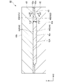


Classifications
-
- H—ELECTRICITY
- H10—SEMICONDUCTOR DEVICES; ELECTRIC SOLID-STATE DEVICES NOT OTHERWISE PROVIDED FOR
- H10P—GENERIC PROCESSES OR APPARATUS FOR THE MANUFACTURE OR TREATMENT OF DEVICES COVERED BY CLASS H10
- H10P72/00—Handling or holding of wafers, substrates or devices during manufacture or treatment thereof
- H10P72/70—Handling or holding of wafers, substrates or devices during manufacture or treatment thereof for supporting or gripping
- H10P72/72—Handling or holding of wafers, substrates or devices during manufacture or treatment thereof for supporting or gripping using electrostatic chucks
- H10P72/722—Details of electrostatic chucks
-
- C—CHEMISTRY; METALLURGY
- C04—CEMENTS; CONCRETE; ARTIFICIAL STONE; CERAMICS; REFRACTORIES
- C04B—LIME, MAGNESIA; SLAG; CEMENTS; COMPOSITIONS THEREOF, e.g. MORTARS, CONCRETE OR LIKE BUILDING MATERIALS; ARTIFICIAL STONE; CERAMICS; REFRACTORIES; TREATMENT OF NATURAL STONE
- C04B35/00—Shaped ceramic products characterised by their composition; Ceramics compositions; Processing powders of inorganic compounds preparatory to the manufacturing of ceramic products
- C04B35/01—Shaped ceramic products characterised by their composition; Ceramics compositions; Processing powders of inorganic compounds preparatory to the manufacturing of ceramic products based on oxide ceramics
- C04B35/03—Shaped ceramic products characterised by their composition; Ceramics compositions; Processing powders of inorganic compounds preparatory to the manufacturing of ceramic products based on oxide ceramics based on magnesium oxide, calcium oxide or oxide mixtures derived from dolomite
- C04B35/04—Shaped ceramic products characterised by their composition; Ceramics compositions; Processing powders of inorganic compounds preparatory to the manufacturing of ceramic products based on oxide ceramics based on magnesium oxide, calcium oxide or oxide mixtures derived from dolomite based on magnesium oxide
- C04B35/053—Fine ceramics
-
- C—CHEMISTRY; METALLURGY
- C04—CEMENTS; CONCRETE; ARTIFICIAL STONE; CERAMICS; REFRACTORIES
- C04B—LIME, MAGNESIA; SLAG; CEMENTS; COMPOSITIONS THEREOF, e.g. MORTARS, CONCRETE OR LIKE BUILDING MATERIALS; ARTIFICIAL STONE; CERAMICS; REFRACTORIES; TREATMENT OF NATURAL STONE
- C04B35/00—Shaped ceramic products characterised by their composition; Ceramics compositions; Processing powders of inorganic compounds preparatory to the manufacturing of ceramic products
- C04B35/01—Shaped ceramic products characterised by their composition; Ceramics compositions; Processing powders of inorganic compounds preparatory to the manufacturing of ceramic products based on oxide ceramics
- C04B35/10—Shaped ceramic products characterised by their composition; Ceramics compositions; Processing powders of inorganic compounds preparatory to the manufacturing of ceramic products based on oxide ceramics based on aluminium oxide
- C04B35/111—Fine ceramics
- C04B35/117—Composites
-
- C—CHEMISTRY; METALLURGY
- C04—CEMENTS; CONCRETE; ARTIFICIAL STONE; CERAMICS; REFRACTORIES
- C04B—LIME, MAGNESIA; SLAG; CEMENTS; COMPOSITIONS THEREOF, e.g. MORTARS, CONCRETE OR LIKE BUILDING MATERIALS; ARTIFICIAL STONE; CERAMICS; REFRACTORIES; TREATMENT OF NATURAL STONE
- C04B35/00—Shaped ceramic products characterised by their composition; Ceramics compositions; Processing powders of inorganic compounds preparatory to the manufacturing of ceramic products
- C04B35/01—Shaped ceramic products characterised by their composition; Ceramics compositions; Processing powders of inorganic compounds preparatory to the manufacturing of ceramic products based on oxide ceramics
- C04B35/14—Shaped ceramic products characterised by their composition; Ceramics compositions; Processing powders of inorganic compounds preparatory to the manufacturing of ceramic products based on oxide ceramics based on silica
-
- C—CHEMISTRY; METALLURGY
- C04—CEMENTS; CONCRETE; ARTIFICIAL STONE; CERAMICS; REFRACTORIES
- C04B—LIME, MAGNESIA; SLAG; CEMENTS; COMPOSITIONS THEREOF, e.g. MORTARS, CONCRETE OR LIKE BUILDING MATERIALS; ARTIFICIAL STONE; CERAMICS; REFRACTORIES; TREATMENT OF NATURAL STONE
- C04B35/00—Shaped ceramic products characterised by their composition; Ceramics compositions; Processing powders of inorganic compounds preparatory to the manufacturing of ceramic products
- C04B35/01—Shaped ceramic products characterised by their composition; Ceramics compositions; Processing powders of inorganic compounds preparatory to the manufacturing of ceramic products based on oxide ceramics
- C04B35/44—Shaped ceramic products characterised by their composition; Ceramics compositions; Processing powders of inorganic compounds preparatory to the manufacturing of ceramic products based on oxide ceramics based on aluminates
-
- C—CHEMISTRY; METALLURGY
- C04—CEMENTS; CONCRETE; ARTIFICIAL STONE; CERAMICS; REFRACTORIES
- C04B—LIME, MAGNESIA; SLAG; CEMENTS; COMPOSITIONS THEREOF, e.g. MORTARS, CONCRETE OR LIKE BUILDING MATERIALS; ARTIFICIAL STONE; CERAMICS; REFRACTORIES; TREATMENT OF NATURAL STONE
- C04B35/00—Shaped ceramic products characterised by their composition; Ceramics compositions; Processing powders of inorganic compounds preparatory to the manufacturing of ceramic products
- C04B35/50—Shaped ceramic products characterised by their composition; Ceramics compositions; Processing powders of inorganic compounds preparatory to the manufacturing of ceramic products based on rare-earth compounds
- C04B35/505—Shaped ceramic products characterised by their composition; Ceramics compositions; Processing powders of inorganic compounds preparatory to the manufacturing of ceramic products based on rare-earth compounds based on yttrium oxide
-
- C—CHEMISTRY; METALLURGY
- C04—CEMENTS; CONCRETE; ARTIFICIAL STONE; CERAMICS; REFRACTORIES
- C04B—LIME, MAGNESIA; SLAG; CEMENTS; COMPOSITIONS THEREOF, e.g. MORTARS, CONCRETE OR LIKE BUILDING MATERIALS; ARTIFICIAL STONE; CERAMICS; REFRACTORIES; TREATMENT OF NATURAL STONE
- C04B35/00—Shaped ceramic products characterised by their composition; Ceramics compositions; Processing powders of inorganic compounds preparatory to the manufacturing of ceramic products
- C04B35/515—Shaped ceramic products characterised by their composition; Ceramics compositions; Processing powders of inorganic compounds preparatory to the manufacturing of ceramic products based on non-oxide ceramics
- C04B35/58—Shaped ceramic products characterised by their composition; Ceramics compositions; Processing powders of inorganic compounds preparatory to the manufacturing of ceramic products based on non-oxide ceramics based on borides, nitrides, i.e. nitrides, oxynitrides, carbonitrides or oxycarbonitrides or silicides
- C04B35/581—Shaped ceramic products characterised by their composition; Ceramics compositions; Processing powders of inorganic compounds preparatory to the manufacturing of ceramic products based on non-oxide ceramics based on borides, nitrides, i.e. nitrides, oxynitrides, carbonitrides or oxycarbonitrides or silicides based on aluminium nitride
-
- C—CHEMISTRY; METALLURGY
- C04—CEMENTS; CONCRETE; ARTIFICIAL STONE; CERAMICS; REFRACTORIES
- C04B—LIME, MAGNESIA; SLAG; CEMENTS; COMPOSITIONS THEREOF, e.g. MORTARS, CONCRETE OR LIKE BUILDING MATERIALS; ARTIFICIAL STONE; CERAMICS; REFRACTORIES; TREATMENT OF NATURAL STONE
- C04B35/00—Shaped ceramic products characterised by their composition; Ceramics compositions; Processing powders of inorganic compounds preparatory to the manufacturing of ceramic products
- C04B35/515—Shaped ceramic products characterised by their composition; Ceramics compositions; Processing powders of inorganic compounds preparatory to the manufacturing of ceramic products based on non-oxide ceramics
- C04B35/58—Shaped ceramic products characterised by their composition; Ceramics compositions; Processing powders of inorganic compounds preparatory to the manufacturing of ceramic products based on non-oxide ceramics based on borides, nitrides, i.e. nitrides, oxynitrides, carbonitrides or oxycarbonitrides or silicides
- C04B35/584—Shaped ceramic products characterised by their composition; Ceramics compositions; Processing powders of inorganic compounds preparatory to the manufacturing of ceramic products based on non-oxide ceramics based on borides, nitrides, i.e. nitrides, oxynitrides, carbonitrides or oxycarbonitrides or silicides based on silicon nitride
-
- C—CHEMISTRY; METALLURGY
- C04—CEMENTS; CONCRETE; ARTIFICIAL STONE; CERAMICS; REFRACTORIES
- C04B—LIME, MAGNESIA; SLAG; CEMENTS; COMPOSITIONS THEREOF, e.g. MORTARS, CONCRETE OR LIKE BUILDING MATERIALS; ARTIFICIAL STONE; CERAMICS; REFRACTORIES; TREATMENT OF NATURAL STONE
- C04B37/00—Joining burned ceramic articles with other burned ceramic articles or other articles by heating
- C04B37/001—Joining burned ceramic articles with other burned ceramic articles or other articles by heating directly with other burned ceramic articles
-
- C—CHEMISTRY; METALLURGY
- C04—CEMENTS; CONCRETE; ARTIFICIAL STONE; CERAMICS; REFRACTORIES
- C04B—LIME, MAGNESIA; SLAG; CEMENTS; COMPOSITIONS THEREOF, e.g. MORTARS, CONCRETE OR LIKE BUILDING MATERIALS; ARTIFICIAL STONE; CERAMICS; REFRACTORIES; TREATMENT OF NATURAL STONE
- C04B37/00—Joining burned ceramic articles with other burned ceramic articles or other articles by heating
- C04B37/003—Joining burned ceramic articles with other burned ceramic articles or other articles by heating by means of an interlayer consisting of a combination of materials selected from glass, or ceramic material with metals, metal oxides or metal salts
-
- C—CHEMISTRY; METALLURGY
- C04—CEMENTS; CONCRETE; ARTIFICIAL STONE; CERAMICS; REFRACTORIES
- C04B—LIME, MAGNESIA; SLAG; CEMENTS; COMPOSITIONS THEREOF, e.g. MORTARS, CONCRETE OR LIKE BUILDING MATERIALS; ARTIFICIAL STONE; CERAMICS; REFRACTORIES; TREATMENT OF NATURAL STONE
- C04B37/00—Joining burned ceramic articles with other burned ceramic articles or other articles by heating
- C04B37/003—Joining burned ceramic articles with other burned ceramic articles or other articles by heating by means of an interlayer consisting of a combination of materials selected from glass, or ceramic material with metals, metal oxides or metal salts
- C04B37/005—Joining burned ceramic articles with other burned ceramic articles or other articles by heating by means of an interlayer consisting of a combination of materials selected from glass, or ceramic material with metals, metal oxides or metal salts consisting of glass or ceramic material
-
- H—ELECTRICITY
- H01—ELECTRIC ELEMENTS
- H01J—ELECTRIC DISCHARGE TUBES OR DISCHARGE LAMPS
- H01J37/00—Discharge tubes with provision for introducing objects or material to be exposed to the discharge, e.g. for the purpose of examination or processing thereof
- H01J37/32—Gas-filled discharge tubes
- H01J37/32431—Constructional details of the reactor
- H01J37/32715—Workpiece holder
-
- H—ELECTRICITY
- H02—GENERATION; CONVERSION OR DISTRIBUTION OF ELECTRIC POWER
- H02N—ELECTRIC MACHINES NOT OTHERWISE PROVIDED FOR
- H02N13/00—Clutches or holding devices using electrostatic attraction, e.g. using Johnson-Rahbek effect
-
- H—ELECTRICITY
- H10—SEMICONDUCTOR DEVICES; ELECTRIC SOLID-STATE DEVICES NOT OTHERWISE PROVIDED FOR
- H10P—GENERIC PROCESSES OR APPARATUS FOR THE MANUFACTURE OR TREATMENT OF DEVICES COVERED BY CLASS H10
- H10P72/00—Handling or holding of wafers, substrates or devices during manufacture or treatment thereof
- H10P72/04—Apparatus for manufacture or treatment
- H10P72/0431—Apparatus for thermal treatment
- H10P72/0434—Apparatus for thermal treatment mainly by convection
-
- H—ELECTRICITY
- H10—SEMICONDUCTOR DEVICES; ELECTRIC SOLID-STATE DEVICES NOT OTHERWISE PROVIDED FOR
- H10P—GENERIC PROCESSES OR APPARATUS FOR THE MANUFACTURE OR TREATMENT OF DEVICES COVERED BY CLASS H10
- H10P72/00—Handling or holding of wafers, substrates or devices during manufacture or treatment thereof
- H10P72/70—Handling or holding of wafers, substrates or devices during manufacture or treatment thereof for supporting or gripping
-
- H—ELECTRICITY
- H10—SEMICONDUCTOR DEVICES; ELECTRIC SOLID-STATE DEVICES NOT OTHERWISE PROVIDED FOR
- H10P—GENERIC PROCESSES OR APPARATUS FOR THE MANUFACTURE OR TREATMENT OF DEVICES COVERED BY CLASS H10
- H10P72/00—Handling or holding of wafers, substrates or devices during manufacture or treatment thereof
- H10P72/70—Handling or holding of wafers, substrates or devices during manufacture or treatment thereof for supporting or gripping
- H10P72/72—Handling or holding of wafers, substrates or devices during manufacture or treatment thereof for supporting or gripping using electrostatic chucks
-
- H—ELECTRICITY
- H10—SEMICONDUCTOR DEVICES; ELECTRIC SOLID-STATE DEVICES NOT OTHERWISE PROVIDED FOR
- H10P—GENERIC PROCESSES OR APPARATUS FOR THE MANUFACTURE OR TREATMENT OF DEVICES COVERED BY CLASS H10
- H10P72/00—Handling or holding of wafers, substrates or devices during manufacture or treatment thereof
- H10P72/70—Handling or holding of wafers, substrates or devices during manufacture or treatment thereof for supporting or gripping
- H10P72/76—Handling or holding of wafers, substrates or devices during manufacture or treatment thereof for supporting or gripping using mechanical means, e.g. clamps or pinches
- H10P72/7604—Handling or holding of wafers, substrates or devices during manufacture or treatment thereof for supporting or gripping using mechanical means, e.g. clamps or pinches the wafers being placed on a susceptor, stage or support
- H10P72/7616—Handling or holding of wafers, substrates or devices during manufacture or treatment thereof for supporting or gripping using mechanical means, e.g. clamps or pinches the wafers being placed on a susceptor, stage or support characterised by a coating, a hardness or a material
-
- C—CHEMISTRY; METALLURGY
- C04—CEMENTS; CONCRETE; ARTIFICIAL STONE; CERAMICS; REFRACTORIES
- C04B—LIME, MAGNESIA; SLAG; CEMENTS; COMPOSITIONS THEREOF, e.g. MORTARS, CONCRETE OR LIKE BUILDING MATERIALS; ARTIFICIAL STONE; CERAMICS; REFRACTORIES; TREATMENT OF NATURAL STONE
- C04B2235/00—Aspects relating to ceramic starting mixtures or sintered ceramic products
- C04B2235/02—Composition of constituents of the starting material or of secondary phases of the final product
- C04B2235/30—Constituents and secondary phases not being of a fibrous nature
- C04B2235/32—Metal oxides, mixed metal oxides, or oxide-forming salts thereof, e.g. carbonates, nitrates, (oxy)hydroxides, chlorides
- C04B2235/3224—Rare earth oxide or oxide forming salts thereof, e.g. scandium oxide
- C04B2235/3225—Yttrium oxide or oxide-forming salts thereof
-
- C—CHEMISTRY; METALLURGY
- C04—CEMENTS; CONCRETE; ARTIFICIAL STONE; CERAMICS; REFRACTORIES
- C04B—LIME, MAGNESIA; SLAG; CEMENTS; COMPOSITIONS THEREOF, e.g. MORTARS, CONCRETE OR LIKE BUILDING MATERIALS; ARTIFICIAL STONE; CERAMICS; REFRACTORIES; TREATMENT OF NATURAL STONE
- C04B2235/00—Aspects relating to ceramic starting mixtures or sintered ceramic products
- C04B2235/02—Composition of constituents of the starting material or of secondary phases of the final product
- C04B2235/30—Constituents and secondary phases not being of a fibrous nature
- C04B2235/32—Metal oxides, mixed metal oxides, or oxide-forming salts thereof, e.g. carbonates, nitrates, (oxy)hydroxides, chlorides
- C04B2235/3231—Refractory metal oxides, their mixed metal oxides, or oxide-forming salts thereof
- C04B2235/3232—Titanium oxides or titanates, e.g. rutile or anatase
-
- C—CHEMISTRY; METALLURGY
- C04—CEMENTS; CONCRETE; ARTIFICIAL STONE; CERAMICS; REFRACTORIES
- C04B—LIME, MAGNESIA; SLAG; CEMENTS; COMPOSITIONS THEREOF, e.g. MORTARS, CONCRETE OR LIKE BUILDING MATERIALS; ARTIFICIAL STONE; CERAMICS; REFRACTORIES; TREATMENT OF NATURAL STONE
- C04B2235/00—Aspects relating to ceramic starting mixtures or sintered ceramic products
- C04B2235/02—Composition of constituents of the starting material or of secondary phases of the final product
- C04B2235/30—Constituents and secondary phases not being of a fibrous nature
- C04B2235/38—Non-oxide ceramic constituents or additives
- C04B2235/3817—Carbides
- C04B2235/3826—Silicon carbides
-
- C—CHEMISTRY; METALLURGY
- C04—CEMENTS; CONCRETE; ARTIFICIAL STONE; CERAMICS; REFRACTORIES
- C04B—LIME, MAGNESIA; SLAG; CEMENTS; COMPOSITIONS THEREOF, e.g. MORTARS, CONCRETE OR LIKE BUILDING MATERIALS; ARTIFICIAL STONE; CERAMICS; REFRACTORIES; TREATMENT OF NATURAL STONE
- C04B2235/00—Aspects relating to ceramic starting mixtures or sintered ceramic products
- C04B2235/02—Composition of constituents of the starting material or of secondary phases of the final product
- C04B2235/30—Constituents and secondary phases not being of a fibrous nature
- C04B2235/38—Non-oxide ceramic constituents or additives
- C04B2235/3817—Carbides
- C04B2235/3839—Refractory metal carbides
-
- C—CHEMISTRY; METALLURGY
- C04—CEMENTS; CONCRETE; ARTIFICIAL STONE; CERAMICS; REFRACTORIES
- C04B—LIME, MAGNESIA; SLAG; CEMENTS; COMPOSITIONS THEREOF, e.g. MORTARS, CONCRETE OR LIKE BUILDING MATERIALS; ARTIFICIAL STONE; CERAMICS; REFRACTORIES; TREATMENT OF NATURAL STONE
- C04B2235/00—Aspects relating to ceramic starting mixtures or sintered ceramic products
- C04B2235/02—Composition of constituents of the starting material or of secondary phases of the final product
- C04B2235/30—Constituents and secondary phases not being of a fibrous nature
- C04B2235/38—Non-oxide ceramic constituents or additives
- C04B2235/3817—Carbides
- C04B2235/3839—Refractory metal carbides
- C04B2235/3843—Titanium carbides
-
- C—CHEMISTRY; METALLURGY
- C04—CEMENTS; CONCRETE; ARTIFICIAL STONE; CERAMICS; REFRACTORIES
- C04B—LIME, MAGNESIA; SLAG; CEMENTS; COMPOSITIONS THEREOF, e.g. MORTARS, CONCRETE OR LIKE BUILDING MATERIALS; ARTIFICIAL STONE; CERAMICS; REFRACTORIES; TREATMENT OF NATURAL STONE
- C04B2235/00—Aspects relating to ceramic starting mixtures or sintered ceramic products
- C04B2235/02—Composition of constituents of the starting material or of secondary phases of the final product
- C04B2235/30—Constituents and secondary phases not being of a fibrous nature
- C04B2235/38—Non-oxide ceramic constituents or additives
- C04B2235/3852—Nitrides, e.g. oxynitrides, carbonitrides, oxycarbonitrides, lithium nitride, magnesium nitride
- C04B2235/3886—Refractory metal nitrides, e.g. vanadium nitride, tungsten nitride
-
- C—CHEMISTRY; METALLURGY
- C04—CEMENTS; CONCRETE; ARTIFICIAL STONE; CERAMICS; REFRACTORIES
- C04B—LIME, MAGNESIA; SLAG; CEMENTS; COMPOSITIONS THEREOF, e.g. MORTARS, CONCRETE OR LIKE BUILDING MATERIALS; ARTIFICIAL STONE; CERAMICS; REFRACTORIES; TREATMENT OF NATURAL STONE
- C04B2235/00—Aspects relating to ceramic starting mixtures or sintered ceramic products
- C04B2235/02—Composition of constituents of the starting material or of secondary phases of the final product
- C04B2235/30—Constituents and secondary phases not being of a fibrous nature
- C04B2235/40—Metallic constituents or additives not added as binding phase
- C04B2235/404—Refractory metals
-
- C—CHEMISTRY; METALLURGY
- C04—CEMENTS; CONCRETE; ARTIFICIAL STONE; CERAMICS; REFRACTORIES
- C04B—LIME, MAGNESIA; SLAG; CEMENTS; COMPOSITIONS THEREOF, e.g. MORTARS, CONCRETE OR LIKE BUILDING MATERIALS; ARTIFICIAL STONE; CERAMICS; REFRACTORIES; TREATMENT OF NATURAL STONE
- C04B2235/00—Aspects relating to ceramic starting mixtures or sintered ceramic products
- C04B2235/02—Composition of constituents of the starting material or of secondary phases of the final product
- C04B2235/30—Constituents and secondary phases not being of a fibrous nature
- C04B2235/42—Non metallic elements added as constituents or additives, e.g. sulfur, phosphor, selenium or tellurium
- C04B2235/422—Carbon
-
- C—CHEMISTRY; METALLURGY
- C04—CEMENTS; CONCRETE; ARTIFICIAL STONE; CERAMICS; REFRACTORIES
- C04B—LIME, MAGNESIA; SLAG; CEMENTS; COMPOSITIONS THEREOF, e.g. MORTARS, CONCRETE OR LIKE BUILDING MATERIALS; ARTIFICIAL STONE; CERAMICS; REFRACTORIES; TREATMENT OF NATURAL STONE
- C04B2235/00—Aspects relating to ceramic starting mixtures or sintered ceramic products
- C04B2235/02—Composition of constituents of the starting material or of secondary phases of the final product
- C04B2235/50—Constituents or additives of the starting mixture chosen for their shape or used because of their shape or their physical appearance
- C04B2235/54—Particle size related information
- C04B2235/5418—Particle size related information expressed by the size of the particles or aggregates thereof
- C04B2235/5436—Particle size related information expressed by the size of the particles or aggregates thereof micrometer sized, i.e. from 1 to 100 micron
-
- C—CHEMISTRY; METALLURGY
- C04—CEMENTS; CONCRETE; ARTIFICIAL STONE; CERAMICS; REFRACTORIES
- C04B—LIME, MAGNESIA; SLAG; CEMENTS; COMPOSITIONS THEREOF, e.g. MORTARS, CONCRETE OR LIKE BUILDING MATERIALS; ARTIFICIAL STONE; CERAMICS; REFRACTORIES; TREATMENT OF NATURAL STONE
- C04B2235/00—Aspects relating to ceramic starting mixtures or sintered ceramic products
- C04B2235/02—Composition of constituents of the starting material or of secondary phases of the final product
- C04B2235/50—Constituents or additives of the starting mixture chosen for their shape or used because of their shape or their physical appearance
- C04B2235/54—Particle size related information
- C04B2235/5418—Particle size related information expressed by the size of the particles or aggregates thereof
- C04B2235/5445—Particle size related information expressed by the size of the particles or aggregates thereof submicron sized, i.e. from 0,1 to 1 micron
-
- C—CHEMISTRY; METALLURGY
- C04—CEMENTS; CONCRETE; ARTIFICIAL STONE; CERAMICS; REFRACTORIES
- C04B—LIME, MAGNESIA; SLAG; CEMENTS; COMPOSITIONS THEREOF, e.g. MORTARS, CONCRETE OR LIKE BUILDING MATERIALS; ARTIFICIAL STONE; CERAMICS; REFRACTORIES; TREATMENT OF NATURAL STONE
- C04B2235/00—Aspects relating to ceramic starting mixtures or sintered ceramic products
- C04B2235/70—Aspects relating to sintered or melt-casted ceramic products
- C04B2235/74—Physical characteristics
- C04B2235/76—Crystal structural characteristics, e.g. symmetry
- C04B2235/762—Cubic symmetry, e.g. beta-SiC
- C04B2235/764—Garnet structure A3B2(CO4)3
-
- C—CHEMISTRY; METALLURGY
- C04—CEMENTS; CONCRETE; ARTIFICIAL STONE; CERAMICS; REFRACTORIES
- C04B—LIME, MAGNESIA; SLAG; CEMENTS; COMPOSITIONS THEREOF, e.g. MORTARS, CONCRETE OR LIKE BUILDING MATERIALS; ARTIFICIAL STONE; CERAMICS; REFRACTORIES; TREATMENT OF NATURAL STONE
- C04B2235/00—Aspects relating to ceramic starting mixtures or sintered ceramic products
- C04B2235/70—Aspects relating to sintered or melt-casted ceramic products
- C04B2235/74—Physical characteristics
- C04B2235/77—Density
- C04B2235/775—Products showing a density-gradient
-
- C—CHEMISTRY; METALLURGY
- C04—CEMENTS; CONCRETE; ARTIFICIAL STONE; CERAMICS; REFRACTORIES
- C04B—LIME, MAGNESIA; SLAG; CEMENTS; COMPOSITIONS THEREOF, e.g. MORTARS, CONCRETE OR LIKE BUILDING MATERIALS; ARTIFICIAL STONE; CERAMICS; REFRACTORIES; TREATMENT OF NATURAL STONE
- C04B2237/00—Aspects relating to ceramic laminates or to joining of ceramic articles with other articles by heating
- C04B2237/02—Aspects relating to interlayers, e.g. used to join ceramic articles with other articles by heating
- C04B2237/04—Ceramic interlayers
- C04B2237/06—Oxidic interlayers
- C04B2237/064—Oxidic interlayers based on alumina or aluminates
-
- C—CHEMISTRY; METALLURGY
- C04—CEMENTS; CONCRETE; ARTIFICIAL STONE; CERAMICS; REFRACTORIES
- C04B—LIME, MAGNESIA; SLAG; CEMENTS; COMPOSITIONS THEREOF, e.g. MORTARS, CONCRETE OR LIKE BUILDING MATERIALS; ARTIFICIAL STONE; CERAMICS; REFRACTORIES; TREATMENT OF NATURAL STONE
- C04B2237/00—Aspects relating to ceramic laminates or to joining of ceramic articles with other articles by heating
- C04B2237/02—Aspects relating to interlayers, e.g. used to join ceramic articles with other articles by heating
- C04B2237/04—Ceramic interlayers
- C04B2237/08—Non-oxidic interlayers
- C04B2237/083—Carbide interlayers, e.g. silicon carbide interlayers
-
- C—CHEMISTRY; METALLURGY
- C04—CEMENTS; CONCRETE; ARTIFICIAL STONE; CERAMICS; REFRACTORIES
- C04B—LIME, MAGNESIA; SLAG; CEMENTS; COMPOSITIONS THEREOF, e.g. MORTARS, CONCRETE OR LIKE BUILDING MATERIALS; ARTIFICIAL STONE; CERAMICS; REFRACTORIES; TREATMENT OF NATURAL STONE
- C04B2237/00—Aspects relating to ceramic laminates or to joining of ceramic articles with other articles by heating
- C04B2237/30—Composition of layers of ceramic laminates or of ceramic or metallic articles to be joined by heating, e.g. Si substrates
- C04B2237/32—Ceramic
- C04B2237/34—Oxidic
- C04B2237/343—Alumina or aluminates
-
- C—CHEMISTRY; METALLURGY
- C04—CEMENTS; CONCRETE; ARTIFICIAL STONE; CERAMICS; REFRACTORIES
- C04B—LIME, MAGNESIA; SLAG; CEMENTS; COMPOSITIONS THEREOF, e.g. MORTARS, CONCRETE OR LIKE BUILDING MATERIALS; ARTIFICIAL STONE; CERAMICS; REFRACTORIES; TREATMENT OF NATURAL STONE
- C04B2237/00—Aspects relating to ceramic laminates or to joining of ceramic articles with other articles by heating
- C04B2237/50—Processing aspects relating to ceramic laminates or to the joining of ceramic articles with other articles by heating
- C04B2237/64—Forming laminates or joined articles comprising grooves or cuts
-
- C—CHEMISTRY; METALLURGY
- C04—CEMENTS; CONCRETE; ARTIFICIAL STONE; CERAMICS; REFRACTORIES
- C04B—LIME, MAGNESIA; SLAG; CEMENTS; COMPOSITIONS THEREOF, e.g. MORTARS, CONCRETE OR LIKE BUILDING MATERIALS; ARTIFICIAL STONE; CERAMICS; REFRACTORIES; TREATMENT OF NATURAL STONE
- C04B2237/00—Aspects relating to ceramic laminates or to joining of ceramic articles with other articles by heating
- C04B2237/50—Processing aspects relating to ceramic laminates or to the joining of ceramic articles with other articles by heating
- C04B2237/68—Forming laminates or joining articles wherein at least one substrate contains at least two different parts of macro-size, e.g. one ceramic substrate layer containing an embedded conductor or electrode
-
- H—ELECTRICITY
- H01—ELECTRIC ELEMENTS
- H01J—ELECTRIC DISCHARGE TUBES OR DISCHARGE LAMPS
- H01J2237/00—Discharge tubes exposing object to beam, e.g. for analysis treatment, etching, imaging
- H01J2237/20—Positioning, supporting, modifying or maintaining the physical state of objects being observed or treated
- H01J2237/2007—Holding mechanisms
Definitions
- the present invention relates to a ceramic joint, an electrostatic chuck device, and a method for manufacturing the ceramic joint.
- a plate-shaped sample such as a silicon wafer is fixed to a predetermined electrostatic chuck member having an electrostatic chuck function by electrostatic adsorption. Processing is applied.
- the surface of the plate-shaped sample becomes hot due to the heat of the plasma, and the resist film on the surface is torn (burst).
- an electrostatic chuck device having a cooling function is used.
- Such an electrostatic chuck device includes the above-mentioned electrostatic chuck member and a temperature control base member in which a flow path for circulating a cooling medium for temperature control is formed inside the metal member.
- the electrostatic chuck member and the temperature control base member are joined and integrated on the lower surface of the electrostatic chuck member via a silicone-based adhesive.
- a cooling medium for temperature adjustment is circulated in the flow path of the temperature adjustment base member to exchange heat, and the temperature of the plate-shaped sample fixed to the upper surface of the electrostatic chuck member is desirable and constant. Electrostatic adsorption is possible while maintaining the temperature. Therefore, by using the electrostatic chuck device, it is possible to perform various plasma treatments on the plate-shaped sample while maintaining the temperature of the plate-shaped sample that is electrostatically adsorbed.
- the electrostatic chuck member As the electrostatic chuck member, a configuration including a pair of ceramic plates and a ceramic joint including an electrode layer interposed between them is known.
- a method for manufacturing such a ceramic joint for example, a groove is dug in one of the ceramic sintered bodies, a conductive layer is formed in the groove, and the conductive layer is ground and mirror-polished together with the ceramic sintered body. Later, a method of joining one ceramic sintered body to the other ceramic sintered body by hot pressing is known (see, for example, Patent Document 1).
- a minute space may remain at the interface (bonding interface) where a pair of ceramic plates are bonded together, and this mechanism reduces the withstand voltage of the electrostatic chuck member, that is, dielectric breakdown.
- the fear has been pointed out.
- the electrostatic chuck member having such a void when a high voltage is applied to the dielectric layer (ceramic plate), it is expected that the electric charge accumulates in the void and the ceramic plate undergoes dielectric breakdown rather than being discharged.
- Patent Document 1 could not sufficiently suppress the formation of voids between the electrode layer and the ceramic plate.
- the present invention has been made in view of the above circumstances, and is an electrostatic chuck including a ceramic joint and a ceramic joint that suppresses dielectric breakdown of a ceramic plate due to electric discharge when a high voltage is applied. It is an object of the present invention to provide an apparatus and a method for manufacturing a ceramic joint.
- the present invention includes the following aspects.
- a pair of ceramic plates and an electrode layer interposed between the pair of ceramic plates are provided, and the electrode layer is embedded in at least one of the pair of ceramic plates, and the pair is formed at the outer edge of the electrode layer.
- a pair of ceramic plates, an electrode layer interposed between the pair of ceramic plates, and an insulating layer arranged around the electrode layer between the pair of ceramic plates are provided, and the outer edge of the electrode layer is provided.
- the insulating ceramic is at least one selected from the group consisting of Al 2 O 3 , Al N, Si 3 N 4 , Y 2 O 3 , YAG, SmAlO 3 , MgO and SiO 2. [3] ] The ceramic joint described in.
- the conductive ceramic is at least one selected from the group consisting of SiC, TiO 2 , TiN, TiC, W, WC, Mo, Mo 2 C and C, according to [3] or [4]. The ceramic junction described.
- An electrostatic chuck device in which an electrostatic chuck member made of ceramics and a temperature control base member made of metal are joined via an adhesive layer, and the electrostatic chuck member is [1]. ] To [7], the electrostatic chuck device comprising the ceramic joint according to any one of the items.
- a method for producing a ceramic bonded body comprising a step of pressurizing the laminated body including the ceramic plate and the electrode layer coating film in the thickness direction while heating.
- An electrode layer forming paste is applied to at least one of the pair of ceramic plates on the surface on which the pair of ceramic plates overlap to form an electrode layer coating film, and the periphery of the electrode layer coating film is formed.
- the pair of ceramic plates are laminated in a step of forming an insulating layer coating film by surrounding the coating film for forming an insulating layer and a posture in which the surface on which the electrode layer coating film and the insulating layer coating film are formed is on the inside.
- the outer edge of the electrode layer coating film and the inner edge of the insulating layer coating film overlap each other, and the contact surface between the electrode layer coating film and the insulating layer coating film is in the thickness direction of the pair of ceramic plates.
- a ceramic joint that suppresses dielectric breakdown of the ceramic plate due to electric discharge when a high voltage is applied an electrostatic chuck device including the ceramic joint, and a method for manufacturing the ceramic joint are provided. Can be provided.
- FIG. 1 the left-right direction of the paper surface (width direction of the ceramic joint) is the X direction, and the vertical direction of the paper (thickness direction of the ceramic joint) is the Y direction.
- the dimensions and ratios of each component are appropriately different in order to make the drawings easier to see.
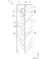
- FIG. 1 is a cross-sectional view showing the ceramic joint of the present embodiment.
- the ceramic joint 1 of the present embodiment includes a pair of ceramic plates 2 and 3 and an electrode layer 4 interposed between the pair of ceramic plates 2 and 3.
- the interface between the members and the inside of the electrode layer may not be solid and a space may be formed.
- the space generated inside the ceramic joint is referred to as "void”, “gap”, and “pore” based on the position and size of generation.
- space is a general term for the above voids, gaps and pores.
- void means a space generated at the interface between the first ceramic plate and the electrode layer or the interface between the second ceramic plate and the electrode layer, and has a major axis of less than 50 ⁇ m.
- gap means a space generated at the interface between the first ceramic plate and the electrode layer or the interface between the second ceramic plate and the electrode layer, and has a major axis of 50 ⁇ m or more.
- pore means the space created inside the electrode layer.
- the major axis of the void and the gap corresponds to the length of the long side of the smallest rectangle circumscribing each space (void or gap).
- the cross-sectional view shown in FIG. 1 is a cross-sectional view obtained by cutting the ceramic joint by a virtual surface including the center of the circle, assuming the smallest circle among the circles circumscribing the ceramic joint 1 in a plan view.
- the ceramic joint 1 is substantially circular in plan view, the center of the circle and the center of the shape of the ceramic joint in plan view are approximately the same.
- the "planar view” refers to a field of view seen from the Y direction, which is the thickness direction of the ceramic joint. Further, in the present specification, the “outer edge” refers to a region near the outer circumference when the object is viewed in a plan view.
- the ceramic plate 2 may be referred to as a first ceramic plate 2
- the ceramic plate 3 may be referred to as a second ceramic plate 3.
- the ceramic joint 1 is a joint in which the first ceramic plate 2 and the second ceramic plate 3 are joined and integrated via the electrode layer 4.
- the outer edge of the electrode layer 4 overlaps the joint surface 5 in a plan view and is not exposed to the outside of the ceramic joint 1. Further, at the outer edge of the electrode layer 4, the bonding surface 5 between the second ceramic plate 3 and the electrode layer 4 is relative to the thickness direction (Y direction in FIG. 1) of the pair of ceramic plates 2 and 3 and the electrode layer 4. Has a tilt. As a result, when the surfaces 4a and 4b of the electrode layers 4 facing each other in the Y direction are compared, the surface 4a on the ⁇ Y side in contact with the first ceramic plate 2 is from the surface 4b on the + Y side in contact with the second ceramic plate 3. Is also wide.
- the second ceramic plate 3 has a + Y direction (thickness direction of the second ceramic plate 3) from the joint surface 3a with the first ceramic plate 2 toward the surface 3b opposite to the joint surface 3a.
- a recessed 3A is formed.
- the opening diameter of the recess 3A gradually decreases in the + Y direction.
- the recess 3A has a bottom surface 3c parallel to the surface 3b of the second ceramic plate 3 and an inclined surface 3d inclined obliquely with respect to the thickness direction of the second ceramic plate 3.
- the inclined surface 3d of the recess 3A is a surface inclined from the bottom surface 3c toward the joint surface 3a.
- the electrode layer 4 is composed of an electrode layer coating film formed by applying (filling) an electrode layer forming paste to the recess 3A. Therefore, the joint surface 5 between the second ceramic plate 3 and the electrode layer 4 is the same surface as the inclined surface 3d of the recess 3A. The electrode layer 4 is embedded in the recess 3A of the second ceramic plate 3.
- the outer edge of the electrode layer 4 has an inclination complementary to the inclined surface 3d of the second ceramic plate 3 and an inclination complementary to the joining surface 3a.
- the length L1 of the joint surface 5 (slope) between the second ceramic plate 3 and the electrode layer 4 is preferably larger than the thickness T1 of the electrode layer 4.
- the electrode layer 4 is a thin electrode having a large spread in the direction orthogonal to the thickness direction rather than the thickness direction.
- the electrode layer 4 has a disk shape with a thickness of 20 ⁇ m and a diameter of 29 cm.
- Such an electrode layer 4 is formed by applying and sintering an electrode layer forming paste, as will be described later.
- the paste for forming the electrode layer shrinks by volume due to sintering, it tends to shrink isotropically, so that the amount of shrinkage is relatively larger in the direction orthogonal to the thickness direction than in the thickness direction. Therefore, voids are structurally likely to occur at the outer edge of the electrode layer 4, that is, at the interface between the electrode layer 4 and the second ceramic plate 3.
- the ratio (L1 / T1) of the length L1 of the joint surface 5 to the thickness T1 of the electrode layer 4 is preferably 1.7 or more and 6.5 or less, more preferably 2.0 or more and 5.0 or less, and 2.2. More than 4.5 or less is more preferable. In addition, L1> T1.
- the length L1 is the length from the position A where the surface 4a and the joint surface 5 are in contact to the position B where the surface 4b and the joint surface 5 are in contact with each other in the cross section of the ceramic joint body 1.
- the position A and the position B can be determined as locations where the tangents of the surfaces 4a and 4b intersect with each other when the tangents of the surfaces 4a and 4b are drawn in the cross section, respectively. Also in other embodiments described later, the positions of both ends of the joint surface, which is a reference for the length of the joint surface, are determined by the same method.
- the ratio (L1 / T1) is within the above range, the generation of voids between the second ceramic plate 3 and the electrode layer 4 is suppressed, and the second ceramic plate 3 and the electrode layer 4 are sufficiently brought into close contact with each other. Can be done.
- a high voltage is applied to the ceramic joint body 1
- electric charges are less likely to accumulate at the joint interface between the second ceramic plate 3 and the electrode layer 4.
- the electric discharge caused by the electric field accumulated at the joint interface can be suppressed, and the dielectric breakdown of the ceramic joint 1 due to the electric discharge can be suppressed.
- the "joining ratio of the joining surface 5 between the ceramic plate 3 and the electrode layer 4" can be calculated from an arbitrary scanning electron micrograph of the joining surface 5. That is, an electron micrograph with a magnifying magnification of 1000 times was taken in a randomly selected field of view (a cross section randomly prepared for the ceramic junction 1), and the length of the inclined surface shown in this electron micrograph. Is "the total length of the joint surface 5 (L1)".
- the major axis length of each void generated between the ceramic plate 3 and the electrode layer 4 is obtained, and the total of the major axis lengths is "the void length (D1) generated on the joint surface 5". And.
- the ratio of the "total length of the joint surface 5 (L1)" to the “void length (D1) generated on the joint surface 5" was obtained as a percentage, and the obtained value was calculated from 100%.
- the subtracted value is calculated as "the joining ratio of the joining surface 5 between the ceramic plate 3 and the electrode layer 4".
- the bonding ratio of the bonding surface 5 between the ceramic plate 3 and the electrode layer 4 is preferably 25% or more, more preferably 40% or more, further preferably 50% or more, still more preferably 60% or more.
- the bonding ratio of the bonding surface 5 between the ceramic plate 3 and the electrode layer 4 is equal to or higher than the above lower limit, the bonding interface between the second ceramic plate 3 and the electrode layer 4 when a high voltage is applied to the ceramic bonding body 1. It is possible to suppress the discharge in. As a result, dielectric breakdown of the ceramic joint 1 due to electric discharge can be suppressed.
- the first ceramic plate 2 and the second ceramic plate 3 have the same shape of the outer periphery of the superposed surface thereof.
- the thicknesses of the first ceramic plate 2 and the second ceramic plate 3 are not particularly limited, and are appropriately adjusted according to the use of the ceramic joint 1.
- the first ceramic plate 2 and the second ceramic plate 3 have the same composition or the same main component.
- the first ceramic plate 2 and the second ceramic plate 3 are preferably made of a composite of an insulating substance and a conductive substance, but may be an insulating substance.
- the insulating material contained in the first ceramic plate 2 and the second ceramic plate 3 is not particularly limited, and is, for example, aluminum oxide (Al 2 O 3 ), aluminum nitride (Al N), yttrium oxide (Y 2 O 3 ). ), Yttrium aluminum garnet (YAG) and the like. Of these, Al 2 O 3 and Al N are preferable.
- the conductive substance contained in the first ceramic plate 2 and the second ceramic plate 3 may be a conductive ceramic or a conductive material such as a carbon material.
- the conductive material contained in the first ceramic plate 2 and the second ceramic plate 3 is not particularly limited, and for example, silicon carbide (SiC), titanium oxide (TIO 2 ), titanium nitride (TiN), titanium carbide (Titanium carbide) ( TiC), carbon materials, rare earth oxides, rare earth fluorides and the like can be mentioned.
- the carbon material include carbon nanotubes (CNTs) and carbon nanofibers. Of these, SiC is preferable.
- the materials of the first ceramic plate 2 and the second ceramic plate 3 have a volume resistivity of 10 13 ⁇ ⁇ cm or more and 10 17 ⁇ ⁇ cm or less, have mechanical strength, and are corrosive gas.
- the material is not particularly limited as long as it is a material having durability against the plasma. Examples of such a material include an Al2O3 sintered body, an AlN sintered body , an Al2O3 - SiC composite sintered body and the like. From the viewpoint of dielectric properties at high temperature, high corrosion resistance, plasma resistance, and heat resistance, the material of the first ceramic plate 2 and the second ceramic plate 3 is preferably an Al2O3 -SiC composite sintered body.
- the average primary particle diameter of the insulating substance constituting the first ceramic plate 2 and the second ceramic plate 3 is preferably 0.5 ⁇ m or more and 3.0 ⁇ m or less, and more preferably 0.7 ⁇ m or more and 2.0 ⁇ m or less. More preferably, it is 0.0 ⁇ m or more and 2.0 ⁇ m or less.
- the first ceramic plate 2 and the second ceramic plate 3 When the average primary particle diameter of the insulating substance constituting the first ceramic plate 2 and the second ceramic plate 3 is 0.5 ⁇ m or more and 3.0 ⁇ m or less, the first ceramic plate is dense, has high withstand voltage resistance, and has high durability. The ceramic plate 2 of 1 and the second ceramic plate 3 are obtained.
- the method for measuring the average primary particle diameter of the insulating substance constituting the first ceramic plate 2 and the second ceramic plate 3 is as follows.
- the first ceramic plate 2 and the second ceramic plate 3 were magnified 10,000 times with an electrolytic emission scanning electron microscope (FE-SEM. JSM-7800F-Prime manufactured by JEOL Ltd.) manufactured by JEOL Ltd. Observe the cut surface in the thickness direction, and use the intercept method to take the average of the particle sizes of 200 insulating substances as the average primary particle size.
- the electrode layer 4 is an electrode for plasma generation for energizing high-frequency power to generate plasma and processing plasma, an electrode for electrostatic chuck for generating electric charge and fixing a plate-shaped sample by electrostatic adsorption force, and an electrode for electrostatic chuck. It is configured to be used as a heater electrode or the like for heating a plate-shaped sample by generating heat by energization.
- the shape (shape when the electrode layer 4 is viewed in a plan view) and the size (thickness and area when the electrode layer 4 is viewed in a plan view) of the electrode layer 4 are not particularly limited, and are used for the ceramic bonded body 1. It will be adjusted accordingly.
- the electrode layer 4 is composed of a composite material (sintered body) of particles of insulating ceramics (insulating substance) and particles of conductive ceramics (conductive substance).
- the insulating ceramics contained in the electrode layer 4 are not particularly limited, and are, for example, Al 2 O 3 , Al N, silicon nitride (Si 3 N 4 ), Y 2 O 3 , YAG, and sumalium-aluminum oxide (SmAlO 3 ). , At least one selected from the group consisting of magnesium oxide (MgO) and silicon oxide (SiO 2 ) is preferable.
- the conductive ceramics (conductive material) contained in the electrode layer 4 are SiC, TiO 2 , TiN, TiC, tungsten (W), tungsten carbide (WC), molybdenum (Mo), molybdenum carbide (Mo 2 C), and carbon. At least one selected from the group consisting of materials and conductive composite sintered bodies is preferred.
- Examples of carbon materials include carbon black, carbon nanotubes, and carbon nanofibers.
- Examples of the conductive composite sintered body include Al 2 O 3 -Ta 4 C 5 , Al 2 O 3 -W, Al 2 O 3 -SiC, AlN-W, AlN-Ta and the like.
- the conductive substance contained in the electrode layer 4 is at least one selected from the group consisting of the substances, the conductivity of the electrode layer can be ensured.
- the electrode layer 4 is made of the above-mentioned conductive substance and insulating substance, the bonding strength between the first ceramic plate 2 and the second ceramic plate 3 and the mechanical strength as an electrode are increased.
- the insulating substance contained in the electrode layer 4 is Al 2 O 3 , the dielectric property at high temperature, high corrosion resistance, plasma resistance, and heat resistance are maintained.
- the ratio (blending ratio) of the contents of the conductive substance and the insulating substance in the electrode layer 4 is not particularly limited, and is appropriately adjusted according to the use of the ceramic joint 1.
- the entire electrode layer 4 may have the same relative density. Further, the electrode layer 4 may have a lower density at the outer edge than the center of the electrode layer 4. The density (relative density) of the electrode layer 4 is determined based on a micrograph taken of the cross section of the ceramic joint 1.
- a microscope for example, a digital microscope (VFX-900F) manufactured by KEYENCE Corporation
- VFX-900F digital microscope
- the imaging range is the outer edge of the electrode layer 4 and is a region overlapping the joint surface 5 in a plan view.
- FIG. 1 when a line parallel to the Y axis is extended from position B toward the first ceramic plate 2, the position where the parallel line and the first ceramic plate 2 intersect is positioned.
- the outer edge portion of the electrode layer 4 surrounded by the positions A, B, and C corresponds.
- the "outer edge portion of the electrode layer 4 surrounded by the positions A, B, and C" is hereinafter referred to as a "density measurement region".
- the region where the conductive ceramics and the insulating ceramics constituting the electrode layer 4 exist (the region where the substance exists. Region 1) and the conductive ceramics. It is distinguishable from the region of "pores" (region 2) in which none of the insulating ceramics is present.
- the relative density of the outer edge of the electrode layer 4 is a value obtained by expressing the area in the outer contour of the density measurement region, that is, the ratio of the area of the region 1 to the total area of the region 1 and the region 2 as a percentage. When there are no pores in the electrode layer 4, the relative density in the density measurement region is 100%.
- the imaging range is the region (center) including the center of the electrode layer 4 in the X direction. If it can be reasonably determined from the micrograph that the density is similar to that of the center of the electrode layer 4, the imaging range does not have to strictly include the center of the electrode layer 4.
- the electrode layer 4 included in the range of width 150 ⁇ m in the X direction is defined as the “density measurement region”, and the electrode layer 4 is calculated in the same manner as in the case of measuring the density of the outer edge of the electrode layer 4.
- the relative density of the center of is obtained.
- the relative density of the outer edge of the electrode layer 4 is preferably 50% or more, more preferably 55% or more.
- the relative density of the outer edge of the electrode layer 4 is less than 50%, resistance heat generation is likely to occur as compared with the case of high density, and the in-plane temperature uniformity when high frequency power is applied is likely to decrease.
- the ceramic junction in which the relative density of the outer edge of the electrode layer 4 is 50% or more the in-plane temperature uniformity is maintained when high frequency power is applied.
- the region where the relative density of the electrode layer 4 is 100% includes the center in the X direction and is 95% or more with respect to the total width, and the region where the relative density of the electrode layer 4 is lower than the center is. , 2.5% from both ends in the X direction, totaling 5% or less.
- the joint surface 5 between the second ceramic plate 3 and the electrode layer 4 has the thickness of the pair of ceramic plates 2 and 3 and the electrode layer 4. It has an inclination with respect to the direction (Y direction in FIG. 1).
- the outer end surface of the electrode layer 4 and the second ceramic plate 3 are easily bonded at the time of manufacture, and the second ceramic plate 3 and the electrode layer 4 are easily joined.
- the generation of voids between them is suppressed, and the second ceramic plate 3 and the electrode layer 4 can be sufficiently brought into close contact with each other.
- discharge at the joint interface between the second ceramic plate 3 and the electrode layer 4 can be suppressed.
- dielectric breakdown of the ceramic joint 1 due to electric discharge can be suppressed.
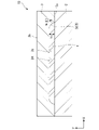
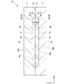
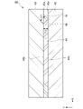
- FIGS. 2 to 4 are cross-sectional views showing a ceramic joint of a modified example, and are cross-sectional views corresponding to FIG. 1.
- Modification 1 In the modified ceramic joint 10 shown in FIG. 2, at the outer edge of the electrode layer 4, the joint surface 5 between the second ceramic plate 3 and the electrode layer 4 has the thickness of the pair of ceramic plates 2 and 3 and the electrode layer 4. It has an inclination with respect to the vertical direction (Y direction in FIG. 2).
- the second ceramic plate 3 is recessed from the joint surface 3a with the first ceramic plate 2 toward the surface 3b opposite to the joint surface 3a (in the thickness direction of the second ceramic plate 3).
- a recess 3A is formed.
- the recess 3A has a bottom surface 3c parallel to the surface 3b of the second ceramic plate 3 and an inclined surface 3d inclined in a curved shape with respect to the thickness direction of the second ceramic plate 3.
- the inclined surface 3d is convex in the + Y direction.
- the electrode layer 4 is composed of an electrode layer coating film formed by applying (filling) an electrode layer forming paste to the recess 3A. Therefore, the joint surface 5 between the second ceramic plate 3 and the electrode layer 4 is the same surface as the inclined surface 3d of the recess 3A.
- the outer edge of the electrode layer 4 has an inclination complementary to the inclined surface 3d of the second ceramic plate 3 and an inclination complementary to the joining surface 5.
- the length L2 of the joint surface 5 (curved surface) between the second ceramic plate 3 and the electrode layer 4 is preferably larger than the thickness T1 of the electrode layer 4.
- the length L2 can be defined by the same method as the above-mentioned length L1.
- Modification 2 In the modified ceramic joint 20 shown in FIG. 3, at the outer edge of the electrode layer 4, the joint surface 5A between the second ceramic plate 3 and the electrode layer 4A has the thickness of the pair of ceramic plates 2 and 3 and the electrode layer 4A. It has an inclination with respect to the vertical direction (Y direction in FIG. 3). As a result, when comparing the surfaces 4Aa and 4Ab of the electrode layers 4A facing each other in the Y direction, the surface 4Aa on the ⁇ Y side is wider than the surface 4b on the + Y side in contact with the second ceramic plate 3.
- the joint surface 5B between the first ceramic plate 2 and the electrode layer 4B is relative to the thickness direction (Y direction in FIG. 3) of the pair of ceramic plates 2 and 3 and the electrode layer 4B. Has a tilt.
- the surface 4Ba on the + Y side is wider than the surface 4Bb on the ⁇ Y side in contact with the first ceramic plate 2.
- the electrode layer 4A and the electrode layer 4B include a joining surface 3a of the second ceramic plate 3 with the first ceramic plate 2 and a joining surface 2a of the first ceramic plate 2 with the second ceramic plate 3. It is in contact with the virtual surface.
- the electrode layer 4A and the electrode layer 4B are integrated in the above virtual surface.
- the tip of the electrode layer 4A (the end in the ⁇ X direction) and the tip of the electrode layer 4B (the end in the ⁇ X direction) are in contact with each other on the virtual surface.
- the second ceramic plate 3 has a + Y direction (thickness direction of the second ceramic plate 3) from the joint surface 3a with the first ceramic plate 2 toward the surface 3b opposite to the joint surface 3a.
- a recessed 3A is formed.
- the recess 3A has a bottom surface 3c parallel to the surface 3b of the second ceramic plate 3 and an inclined surface 3d inclined obliquely with respect to the thickness direction of the second ceramic plate 3.
- the first ceramic plate 2 has a thickness of the first ceramic plate 2 in the ⁇ Y direction from the joint surface 2a with the second ceramic plate 3 toward the surface 2b opposite to the joint surface 2a.
- a recess 2A that is recessed (in the direction) is formed.
- the opening diameter of the recess 2A gradually decreases in the ⁇ Y direction.
- the recess 2A has a bottom surface 2c parallel to the surface 2b of the first ceramic plate 2 and an inclined surface 2d inclined obliquely with respect to the thickness direction of the first ceramic plate 2.
- the inclined surface 2d of the recess 2A is a surface inclined from the bottom surface 2c toward the joint surface 2a.
- the electrode layer 4A is composed of an electrode layer coating film formed by applying (filling) an electrode layer forming paste to the recess 3A. Therefore, the joint surface 5A between the second ceramic plate 3 and the electrode layer 4A is the same surface as the inclined surface 3d of the recess 3A.
- the electrode layer 4B is composed of an electrode layer coating film formed by applying (filling) an electrode layer forming paste to the recess 2A. Therefore, the joint surface 5B between the first ceramic plate 2 and the electrode layer 4B is the same surface as the inclined surface 2d of the recess 2A.
- the outer edge of the electrode layer 4A has an inclination complementary to the inclined surface 3d of the second ceramic plate 3 and an inclination complementary to the joining surface 5A. Further, the outer edge of the electrode layer 4B has an inclination complementary to the inclined surface 2d of the first ceramic plate 2 and an inclination complementary to the joining surface 5B.
- the length L3 of the joint surface 5A (slope) between the second ceramic plate 3 and the electrode layer 4A is preferably larger than the thickness T1 of the electrode layer 4A.
- the length L3 can be defined by the same method as the above-mentioned length L1. In such a ceramic joint 20, the generation of voids between the second ceramic plate 3 and the electrode layer 4A is suppressed, and the second ceramic plate 3 and the electrode layer 4A can be sufficiently brought into close contact with each other.
- the length L4 of the joint surface 5B (slope) between the first ceramic plate 2 and the electrode layer 4B is preferably larger than the thickness T2 of the electrode layer 4B.
- the length L4 can be defined by the same method as the above-mentioned length L1. In such a ceramic joint 20, the generation of voids between the first ceramic plate 2 and the electrode layer 4B is suppressed, and the first ceramic plate 2 and the electrode layer 4B can be sufficiently brought into close contact with each other.
- the first ceramic plate 2 is recessed from the joint surface 2a with the second ceramic plate 3 toward the surface 2b opposite to the joint surface 2a (in the thickness direction of the first ceramic plate 2).
- a recess 2A is formed.
- the recess 2A has a bottom surface 2c parallel to the surface 2b of the first ceramic plate 2 and an inclined surface 2d inclined obliquely with respect to the thickness direction of the first ceramic plate 2.
- the electrode layer 4 is composed of an electrode layer coating film formed by applying (filling) an electrode layer forming paste to the recess 2A. Therefore, the joint surface 5 between the first ceramic plate 2 and the electrode layer 4 is the same surface as the inclined surface 2d of the recess 2A.
- the outer edge of the electrode layer 4 has an inclination complementary to the inclined surface 2d of the first ceramic plate 2 and an inclination complementary to the joining surface 5.
- the length L5 of the joint surface 5 (slope) between the first ceramic plate 2 and the electrode layer 4 is preferably larger than the thickness T2 of the electrode layer 4.
- the length L5 can be defined by the same method as the above-mentioned length L1.
- the generation of voids between the first ceramic plate 2 and the electrode layer 4 is suppressed, and the first ceramic plate 2 and the electrode layer 4 can be sufficiently brought into close contact with each other.
- a high voltage is applied to the ceramic joint body 30 it is possible to suppress discharge at the joint interface between the first ceramic plate 2 and the electrode layer 4.
- dielectric breakdown of the ceramic joint 30 due to electric discharge can be suppressed.
- the method for manufacturing a ceramic joint of the present embodiment has an inclined surface inclined with respect to the thickness direction of the pair of ceramic plates on a surface on which the pair of ceramic plates overlaps with respect to at least one of the pair of ceramic plates.
- a step of forming a recess (hereinafter referred to as "first step") and a step of applying an electrode layer forming paste to the recess to form an electrode layer coating film (hereinafter referred to as "second step”).
- the step of laminating the pair of ceramic plates (hereinafter referred to as "third step”) so that the surface on which the electrode layer coating film is formed is on the inside, and the pair of ceramics. It has a step of pressurizing the laminate including the plate and the electrode layer coating film in the thickness direction while heating (hereinafter, referred to as “fourth step”).
- a recess 3A having an inclined surface 3d inclined with respect to the thickness direction of the second ceramic plate 3 is formed on the joint surface 3a of the second ceramic plate 3.
- the joint surface 3a of the second ceramic plate 3 may be ground or polished.
- the electrode layer forming paste is applied to the recess 3A by a coating method such as a screen printing method to form a coating film (electrode layer coating film) to be the electrode layer 4.
- the outer edge of the electrode layer coating film has an inclination complementary to the inclined surface 3d of the second ceramic plate 3.
- a dispersion liquid in which the particles of the insulating ceramics forming the electrode layer 4 and the particles of the conductive ceramics are dispersed in a solvent is used as the solvent contained in the electrode layer forming paste.
- the first ceramic plate 2 is laminated on the joint surface 3a of the second ceramic plate 3 so that the surface on which the electrode layer coating film is formed is on the inside.
- the laminate including the first ceramic plate 2, the electrode layer coating film, and the second ceramic plate 3 is pressed in the thickness direction while being heated.
- the atmosphere when the laminate is heated and pressed in the thickness direction is preferably a vacuum or an inert atmosphere such as Ar, He, N 2 .
- the "vacuum” means "a state of a space filled with a gas having a pressure lower than the normal atmospheric pressure" as described in JISZ8126-1: 1999.
- the temperature for heating the laminate (heat treatment temperature) is preferably 1400 ° C. or higher and 1900 ° C. or lower, more preferably 1500 ° C. or higher and 1850 ° C. or lower.
- the temperature for heating the laminate is 1400 ° C. or higher and 1900 ° C. or lower, the solvent contained in each coating film is volatilized, and an electrode layer is formed between the first ceramic plate 2 and the second ceramic plate 3. 4 can be formed. Further, the first ceramic plate 2 and the second ceramic plate 3 can be joined and integrated via the electrode layer 4.
- the pressure (pressurizing pressure) for pressurizing the laminate in the thickness direction is preferably 1.0 MPa or more and 50.0 MPa or less, and more preferably 5.0 MPa or more and 20.0 MPa or less.
- the electrode layer 4 can be formed between the first ceramic plate 2 and the second ceramic plate 3. Further, the first ceramic plate 2 and the second ceramic plate 3 can be joined and integrated via the electrode layer 4.
- the electrode layer 4 is embedded in the recess 3A of the second ceramic plate 3, and the outer edge of the electrode layer 4 and the inclined surface 3d of the second ceramic plate 3 are formed. It has a complementary tilt. Therefore, due to the pressurization during sintering, a stress is applied to the outer edge of the electrode layer 4 to press the second ceramic plate 3 from the inclined surface 3d of the second ceramic plate 3. As a result, the outer end surface of the electrode layer 4 and the second ceramic plate 3 are easily joined.
- the method for manufacturing a ceramic joint of the present embodiment it is possible to suppress the generation of voids on the joint surface 5 between the second ceramic plate 3 and the electrode layer 4 at the outer edge of the electrode layer 4.
- the ceramic joint 1 capable of suppressing the discharge on the joint surface 5 and suppressing the dielectric breakdown due to the discharge can be obtained. Can be provided.
- FIG. 5 is a cross-sectional view showing the ceramic joint of the present embodiment, and is a cross-sectional view corresponding to FIG. 1.
- the ceramic joint 40 of the present embodiment includes a pair of ceramic plates 42, 43, and an electrode layer 44 and an insulating layer 45 interposed between the pair of ceramic plates 42, 43.
- the ceramic plate 42 is referred to as a first ceramic plate 42
- the ceramic plate 43 is referred to as a second ceramic plate 43.
- the ceramic joint 40 As shown in FIG. 5, in the ceramic joint 40, the first ceramic plate 42, the electrode layer 44, the insulating layer 45, and the second ceramic plate 43 are laminated in this order.
- the insulating layer 45 is arranged in an annular shape around the electrode layer 44 between the first ceramic plate 42 and the second ceramic plate 43. That is, the ceramic joint 40 is a joint in which the first ceramic plate 42 and the second ceramic plate 43 are joined and integrated via the electrode layer 44 and the insulating layer 45.
- the electrode layer 44 and the insulating layer 45 are provided on the same surface.
- the electrode layer 44 and the insulating layer 45 face the surface (one surface) 42a of the first ceramic plate 42 facing the second ceramic plate 43 and the first ceramic plate 42 of the second ceramic plate 43. It is provided in contact with both surfaces (one surface) 43a.
- the outer edge of the electrode layer 44 overlaps with the insulating layer 45 in a plan view, and is not exposed from the insulating layer 45 to the outside of the ceramic joint 1.
- the joint surface 46 between the electrode layer 44 and the insulating layer 45 has an inclination with respect to the thickness direction (Y direction) of the pair of ceramic plates 42, 43, the electrode layer 44, and the insulating layer 45. ..
- the surfaces 44a and 44b of the electrode layers 44 facing each other in the Y direction are compared, the surface 44a on the ⁇ Y side in contact with the first ceramic plate 42 is from the surface 44b on the + Y side in contact with the second ceramic plate 43. Is also wide.
- the joint surface 46 is an inclined surface that is inclined diagonally with respect to the thickness direction (Y direction in FIG. 5) of the pair of ceramic plates 42, 43, the electrode layer 44, and the insulating layer 45.
- the joint surface 46 faces the surface 42a and is a surface that is inclined from one surface 43a of the second ceramic plate 43 toward one surface 42a of the first ceramic plate 42.
- the outer edge of the electrode layer 44 has a slope complementary to the inclined surface of the second ceramic plate 43, and has a slope complementary to the joint surface 46.
- the length L11 of the joint surface 46 between the electrode layer 44 and the insulating layer 45 is preferably larger than the thickness T11 of the electrode layer 44.
- the length L11 can be defined by the same method as the above-mentioned length L1.
- the generation of voids between the electrode layer 44 and the insulating layer 45 can be suppressed, and the electrode layer 44 and the insulating layer 45 can be sufficiently brought into close contact with each other.
- discharge at the joint interface between the electrode layer 44 and the insulating layer 45 can be suppressed.
- dielectric breakdown of the ceramic joint 40 due to electric discharge can be suppressed.
- voids between the electrode layer 44 and the insulating layer 45 are likely to occur at the outer edge of the electrode layer 44.
- the ratio (L11 / T11) of the length L11 of the joint surface 46 to the thickness T11 of the electrode layer 44 is preferably 1.7 or more and 6.5 or less, more preferably 2.0 or more and 5.0 or less, and 2.2. More than 4.5 or less is more preferable. In addition, L11> T11.
- the ratio (L11 / T11) is within the above range, the generation of voids between the electrode layer 44 and the insulating layer 45 is suppressed, and the electrode layer 44 and the insulating layer 45 can be sufficiently brought into close contact with each other.
- a high voltage is applied to the ceramic joint 40, electric charges are less likely to accumulate at the joint interface between the electrode layer 44 and the insulating layer 45.
- the electric discharge caused by the electric field accumulated at the joint interface can be suppressed, and the dielectric breakdown of the ceramic joint 40 due to the electric discharge can be suppressed.
- the ratio (L11 / T11) is less than the lower limit, the inclination of the joint surface 46 at the time of joining with respect to the Y direction becomes small, so that the adhesion between the electrode layer 44 and the insulating layer 45 decreases.
- the electrode layer 44 and the insulating layer 45 are sufficiently adhered to each other. Further, the ceramic joint in which L11 / T11 is not more than the above upper limit value maintains the in-plane temperature uniformity when high frequency power is applied.
- the "joining ratio of the joining surface 46 between the electrode layer 44 and the insulating layer 45" can be calculated from an arbitrary scanning electron micrograph of the joining surface 46.
- the major axis length of each void generated between the electrode layer 44 and the insulating layer 45 was obtained, and the total of the major axis lengths was "the void length generated on the joint surface 46 (D11)". And.
- the "major axis length (D11)" corresponds to the length of the long side of the smallest rectangle circumscribing each void.
- the ratio of the "total length of the joint surface 46 (L11)" to the “void length (D11) generated in the joint surface 46" was obtained as a percentage, and the obtained value was calculated from 100%.
- the subtracted value is calculated as "the joining ratio of the joining surface 46 between the electrode layer 44 and the insulating layer 45".
- the bonding ratio of the bonding surface 46 between the electrode layer 44, the insulating layer and 45 is preferably 25% or more, more preferably 40% or more, further preferably 50% or more, still more preferably 60% or more.
- a discharge is generated at the bonding interface between the electrode layer 44 and the insulating layer 45 when a high voltage is applied to the ceramic bonding body 40. It can be suppressed. As a result, dielectric breakdown of the ceramic joint 40 due to electric discharge can be suppressed.
- the ceramic plates 42 and 43 have the same configuration as the ceramic plates 2 and 3 described above.
- the electrode layer 44 has the same structure as the above electrode layer 4.
- the insulating layer 45 is configured to join the boundary portion between the first ceramic plate 42 and the second ceramic plate 43, that is, the outer edge region other than the electrode layer 44 forming portion.
- the shape of the insulating layer 45 (the shape when the insulating layer 45 is viewed in a plan view) is not particularly limited, and is appropriately adjusted according to the shape of the electrode layer 44.
- the thickness of the insulating layer 45 is equal to the thickness of the electrode layer 44.
- the insulating layer 45 is made of an insulating substance.
- the insulating substance constituting the insulating layer 45 is not particularly limited, but is preferably the same as the main components of the first ceramic plate 42 and the second ceramic plate 43.
- Examples of the insulating substance constituting the insulating layer 45 include Al 2 O 3 , Al N, Y 2 O 3 , YAG and the like.
- the insulating substance constituting the insulating layer 45 is preferably Al 2 O 3 . Since the insulating substance constituting the insulating layer 45 is Al 2 O 3 , the dielectric property at high temperature, high corrosion resistance, plasma resistance, and heat resistance are maintained.
- the average primary particle size of the insulating substance constituting the insulating layer 45 is preferably 0.5 ⁇ m or more and 3.0 ⁇ m or less, and more preferably 0.7 ⁇ m or more and 2.0 ⁇ m or less.
- the average primary particle diameter of the insulating substance constituting the insulating layer 45 is 0.5 ⁇ m or more, sufficient withstand voltage resistance can be obtained. On the other hand, when the average primary particle diameter of the insulating substance constituting the insulating layer 45 is 3.0 ⁇ m or less, processing such as grinding is easy.
- the method for measuring the average primary particle size of the insulating substance constituting the insulating layer 45 is the same as the method for measuring the average primary particle size of the insulating substance constituting the first ceramic plate 42 and the second ceramic plate 43. ..
- the joint surface 46 between the electrode layer 44 and the insulating layer 45 is the thickness of the pair of ceramic plates 42, 43, the electrode layer 44, and the insulating layer 45. It has an inclination with respect to the vertical direction.
- the outer end surface of the electrode layer 4 and the second ceramic plate 3 can be easily joined at the time of manufacture, and the electrode layer 44 and the insulating layer can be easily joined.
- the generation of voids between the 45 is suppressed, and the electrode layer 44 and the insulating layer 45 can be sufficiently brought into close contact with each other.
- FIGS. 6 to 8 a modified example as shown in FIGS. 6 to 8 may be adopted.
- the same parts as the components in the second embodiment are designated by the same reference numerals, the description thereof will be omitted, and only the different points will be described.
- 6 to 8 are cross-sectional views showing a ceramic joint of a modified example, and are cross-sectional views corresponding to FIG.
- the joint surface 46 between the electrode layer 44 and the insulating layer 45 is a pair of ceramic plates 42, 43, the electrode layer 44, and the insulating layer 45. It has an inclination with respect to the thickness direction (Y direction in FIG. 6).
- the joint surface 46 is an inclined surface that is inclined in a curved shape with respect to the thickness direction (Y direction in FIG. 6) of the pair of ceramic plates 42, 43, the electrode layer 44, and the insulating layer 45.
- the joint surface 46 is convex in the + Y direction.
- the length L12 of the joint surface 46 (curved surface) between the electrode layer 44 and the insulating layer 45 is preferably larger than the thickness T11 of the electrode layer 44.
- the length L11 can be defined by the same method as the above-mentioned length L1.
- the joint surface 46A between the electrode layer 44 and the insulating layer 45 is in the thickness direction of the pair of ceramic plates 42, 43, the electrode layer 44, and the insulating layer 45 (FIG. 7). It has an inclination with respect to the Y direction).
- the first ceramic plate 42 is recessed from one surface 42a toward the surface 42b opposite to the one surface 42a in the ⁇ Y direction (in the thickness direction of the first ceramic plate 42).
- the recess 42A is formed.
- the opening diameter of the recess 42A gradually decreases in the ⁇ Y direction.
- the recess 42A has a bottom surface 42c parallel to the surface 42b of the first ceramic plate 42, and an inclined surface 42d inclined obliquely with respect to the thickness direction of the first ceramic plate 42.
- the inclined surface 42d of the recess 42A faces the second ceramic plate 43, and is a surface inclined from the bottom surface 42c toward one surface 42a.
- the electrode layer forming paste is applied to one surface 43a of the electrode layer 44B and the second ceramic plate 43 formed by applying (filling) the electrode layer forming paste to the recess 42A. It is composed of an electrode layer 44A made of an electrode layer coating film formed by coating. Therefore, the joint surface 46B between the first ceramic plate 42 and the electrode layer 44B is the same surface as the inclined surface 42d of the recess 42B.
- the length L12 of the joint surface 46A between the electrode layer 44A and the insulating layer 45 is preferably larger than the thickness T12 of the electrode layer 44A.
- the length L12 can be defined by the same method as the above-mentioned length L1. In such a ceramic joint 60, the generation of voids between the electrode layer 44A and the insulating layer 45 is suppressed, and the electrode layer 44A and the insulating layer 45 can be sufficiently brought into close contact with each other.
- the length L13 of the joint surface 46B between the first ceramic plate 42 and the electrode layer 44B is larger than the thickness T13 of the electrode layer 44B.
- the length L13 can be defined by the same method as the above-mentioned length L1. In such a ceramic joint 60, the generation of voids between the first ceramic plate 42 and the electrode layer 44B is suppressed, and the first ceramic plate 42 and the electrode layer 44B can be sufficiently brought into close contact with each other.
- the joint surface 46 between the electrode layer 44 and the insulating layer 45 is a pair of ceramic plates 42, 43, the electrode layer 44, and the insulating layer 45. It has an inclination with respect to the thickness direction.
- the joint surface 46 is an inclined surface that is inclined obliquely with respect to the thickness direction (Y direction in FIG. 8) of the pair of ceramic plates 42, 43, the electrode layer 44, and the insulating layer 45.
- the joint surface 46 is a surface that is inclined from one surface 42a of the first ceramic plate 42 toward one surface 43a of the second ceramic plate 43.
- the length L14 of the joint surface 46 between the electrode layer 44 and the insulating layer 45 is preferably larger than the thickness T11 of the electrode layer 44.
- the length L14 can be defined by the same method as the above-mentioned length L1.
- the generation of voids between the electrode layer 44 and the insulating layer 45 is suppressed, and the electrode layer 44 and the insulating layer 45 can be sufficiently brought into close contact with each other.
- discharge at the joint interface between the electrode layer 44 and the insulating layer 45 can be suppressed.
- dielectric breakdown of the ceramic joint 70 due to electric discharge can be suppressed.
- an electrode layer forming paste is applied to at least one of a pair of ceramic plates on the surface where the pair of ceramic plates overlap to form an electrode layer coating film.
- the step of applying the insulating layer forming paste to form the insulating layer coating film (hereinafter referred to as "first step") and the surface on which the electrode layer coating film and the insulating layer coating film are formed are on the inside.
- second step While heating the step of laminating the pair of ceramic plates in the posture (hereinafter referred to as “second step") and the laminate including the pair of ceramic plates, the electrode layer coating film and the insulating layer coating film, It has a step of pressurizing in the thickness direction (hereinafter, referred to as a "third step").
- an electrode layer forming paste is applied to one surface 42a of the first ceramic plate 42 to form an electrode layer coating film, and an insulating layer is formed.
- a forming paste is applied to form an insulating layer coating film. Either the electrode layer coating film or the insulating layer coating film may be formed first.
- the joint surface 46 is insulated from the electrode layer coating film so as to be inclined from one surface 43a of the second ceramic plate 43 toward one surface 42a of the first ceramic plate 42.
- the outer edge of the electrode layer coating has a slope complementary to the inner edge of the insulating layer coating.
- a dispersion liquid in which the insulating ceramic particles forming the electrode layer 44 and the conductive ceramic particles are dispersed in a solvent is used.
- Alcohol such as isopropyl alcohol is used as the solvent contained in the electrode layer forming paste.
- a dispersion liquid in which the insulating ceramics forming the insulating layer 45 is dispersed in a solvent is used.
- Alcohol such as isopropyl alcohol is used as the solvent contained in the paste for forming the insulating layer.
- the second ceramic plate 43 is laminated on one surface 42a of the first ceramic plate 42 so that the surface on which the electrode layer coating film and the insulating layer coating film are formed is on the inside.
- the laminate including the first ceramic plate 42, the electrode layer coating film, the insulating layer coating film, and the second ceramic plate 43 is pressed in the thickness direction while being heated.
- the atmosphere when the laminate is heated and pressed in the thickness direction is preferably a vacuum or an inert atmosphere such as Ar, He, N 2 .
- the temperature for heating the laminate (heat treatment temperature) is preferably 1600 ° C. or higher and 1900 ° C. or lower, and more preferably 1650 ° C. or higher and 1850 ° C. or lower.
- the solvent contained in each coating film is volatilized, and an electrode layer is formed between the first ceramic plate 42 and the second ceramic plate 43.
- the 44 and the insulating layer 45 can be formed. Further, the first ceramic plate 42 and the second ceramic plate 43 can be joined and integrated via the electrode layer 44 and the insulating layer 45.
- the pressure (pressurizing pressure) for pressurizing the laminate in the thickness direction is preferably 1.0 MPa or more and 50.0 MPa or less, and more preferably 5.0 MPa or more and 20.0 MPa or less.
- the pressure for pressurizing the laminate in the thickness direction is 1.0 MPa or more and 50.0 MPa or less
- the electrode layer 44 and the insulating layer in close contact with each other between the first ceramic plate 42 and the second ceramic plate 43. 45 can be formed. Further, the first ceramic plate 42 and the second ceramic plate 43 can be joined and integrated via the electrode layer 44 and the insulating layer 45.
- a ceramic joint of the present embodiment it is possible to suppress the generation of voids on the joint surface 46 between the second ceramic plate 43 and the electrode layer 44 at the outer edge of the electrode layer 44.
- a ceramic joint body 40 which can suppress the discharge on the joint surface 46 and can suppress the dielectric breakdown due to the discharge.
- FIG. 9 is a cross-sectional view showing the electrostatic chuck device of the present embodiment.
- the same components as those of the above-mentioned ceramic joint are designated by the same reference numerals, and overlapping description will be omitted.
- the electrostatic chuck device 100 of the present embodiment has a disk-shaped electrostatic chuck member 102 and a disk-shaped temperature adjusting base member that adjusts the electrostatic chuck member 102 to a desired temperature. It has a 103 and an adhesive layer 104 for joining and integrating the electrostatic chuck member 102 and the temperature adjusting base member 103.
- the electrostatic chuck member 102 is made of, for example, the ceramic joint 1 of the above-described embodiment.
- the mounting surface 111a side of the mounting plate 111 may be described as "upper” and the temperature adjusting base member 103 side may be described as "lower" to represent the relative position of each configuration.
- the electrostatic chuck member 102 has a mounting plate 111 whose upper surface is made of ceramics having a mounting surface 111a on which a plate-shaped sample such as a semiconductor wafer is mounted, and a surface opposite to the mounting surface 111a of the mounting plate 111.
- the support plate 112 provided on the side, the electrostatic adsorption electrode 113 sandwiched between the mounting plate 111 and the support plate 112, and the electrostatic adsorption electrode 113 sandwiched between the mounting plate 111 and the support plate 112 for electrostatic adsorption.
- It has an annular insulating material 114 surrounding the periphery of the electrode 113, and a power feeding terminal 116 provided in a fixing hole 115 of the temperature adjusting base member 103 so as to be in contact with the electrostatic adsorption electrode 113.
- the mounting plate 111 corresponds to the second ceramic plate 43
- the support plate 112 corresponds to the first ceramic plate 42
- the electrostatic adsorption electrode 113 corresponds to the electrode. It corresponds to the layer 44
- the insulating material 114 corresponds to the above-mentioned insulating layer 45.
- a large number of protrusions for supporting a plate-shaped sample such as a semiconductor wafer are erected on the mounting surface 111a of the mounting plate 111 (not shown). Further, on the peripheral edge of the mounting surface 111a of the mounting plate 111, an annular protrusion having a quadrangular cross section is provided so as to go around the peripheral edge so that cooling gas such as helium (He) does not leak. May be. Further, in the region surrounded by the annular protrusions on the mounting surface 111a, a plurality of protrusions having the same height as the annular protrusions, having a circular cross section and a substantially rectangular vertical cross section are provided. May be.
- the thickness of the mounting plate 111 is preferably 0.3 mm or more and 3.0 mm or less, and more preferably 0.5 mm or more and 1.5 mm or less.
- the withstand voltage resistance is excellent.
- the electrostatic attraction force of the electrostatic chuck member 102 does not decrease, and the plate is mounted on the mounting surface 111a of the mounting plate 111.
- the temperature of the plate-shaped sample being processed can be kept at a preferable constant temperature without deteriorating the thermal conductivity between the shaped sample and the temperature adjusting base member 103.
- the support plate 112 supports the mounting plate 111 and the electrostatic adsorption electrode 113 from below.
- the thickness of the support plate 112 is preferably 0.3 mm or more and 3.0 mm or less, and more preferably 0.5 mm or more and 1.5 mm or less. If the thickness of the support plate 112 is 0.3 mm or more, a sufficient withstand voltage can be secured. On the other hand, if the thickness of the support plate 112 is 3.0 mm or less, the electrostatic attraction force of the electrostatic chuck member 102 does not decrease, and the plate shape is mounted on the mounting surface 111a of the mounting plate 111. The temperature of the plate-shaped sample being processed can be kept at a preferable constant temperature without deteriorating the thermal conductivity between the sample and the temperature adjusting base member 103.
- Electrode for electrostatic adsorption In the electrostatic adsorption electrode 113, by applying a voltage, an electrostatic adsorption force for holding the plate-shaped sample is generated on the mounting surface 111a of the mounting plate 111.
- the thickness of the electrostatic adsorption electrode 113 is preferably 5 ⁇ m or more and 200 ⁇ m or less, more preferably 7 ⁇ m or more and 100 ⁇ m or less, and further preferably 10 ⁇ m or more and 100 ⁇ m or less.
- the thickness of the electrostatic adsorption electrode 113 is 5 ⁇ m or more, sufficient conductivity can be ensured.
- the thickness of the electrostatic adsorption electrode 113 is 200 ⁇ m or less, the thermal conductivity between the plate-shaped sample mounted on the mounting surface 111a of the mounting plate 111 and the temperature adjusting base member 103 is high.
- the temperature of the plate-shaped sample being processed can be kept at a desired constant temperature without lowering.
- plasma permeability can be stably generated without deterioration.
- the insulating material 114 is a member that surrounds the electrostatic adsorption electrode 113 and protects the electrostatic adsorption electrode 113 from corrosive gas and its plasma.
- the mounting plate 111 and the support plate 112 are joined and integrated via the electrostatic adsorption electrode 113 by the insulating material 114.
- the power feeding terminal 116 is a member for applying a voltage to the electrostatic adsorption electrode 113.
- the number, shape, and the like of the power feeding terminals 116 are determined by the form of the electrostatic adsorption electrode 113, that is, whether it is a unipolar type or a bipolar type.
- the material of the power supply terminal 116 is not particularly limited as long as it is a conductive material having excellent heat resistance.
- the material of the power feeding terminal 116 is preferably a material whose coefficient of thermal expansion is close to the coefficient of thermal expansion of the electrostatic adsorption electrode 113 and the support plate 112, and is, for example, a metal material such as Kovar alloy or niobium (Nb). , Various conductive ceramics are preferably used.
- the conductive adhesive layer 117 is provided in the fixing hole 115 of the temperature adjusting base member 103 and in the through hole 118 of the support plate 112. Further, the conductive adhesive layer 117 is interposed between the electrostatic adsorption electrode 113 and the power supply terminal 116 to electrically connect the electrostatic adsorption electrode 113 and the power supply terminal 116.
- the conductive adhesive constituting the conductive adhesive layer 117 contains a conductive substance such as carbon fiber and metal powder and a resin.
- the resin contained in the conductive adhesive is not particularly limited as long as it is a resin that is unlikely to cause cohesive failure due to thermal stress, and for example, a silicone resin, an acrylic resin, an epoxy resin, a phenol resin, a polyurethane resin, an unsaturated polyester resin, or the like. Can be mentioned. Among these, a silicone resin is preferable because it has a high degree of expansion and contraction and is unlikely to coagulate and break due to a change in thermal stress.
- the temperature control base member 103 is a thick disk-shaped member made of at least one of metal and ceramics.
- the skeleton of the temperature control base member 103 is configured to also serve as an internal electrode for plasma generation.
- a flow path 121 for circulating a cooling medium such as water, He gas, N 2 gas, etc. is formed inside the skeleton of the temperature control base member 103.
- the skeleton of the temperature control base member 103 is connected to the external high frequency power supply 122. Further, in the fixing hole 115 of the temperature adjusting base member 103, a power feeding terminal 116 whose outer periphery is surrounded by the insulating material 123 is fixed via the insulating material 123. The power supply terminal 116 is connected to an external DC power supply 124.
- the material constituting the temperature control base member 103 is not particularly limited as long as it is a metal having excellent thermal conductivity, conductivity, and workability, or a composite material containing these metals.
- As the material constituting the temperature control base member 103 for example, aluminum (Al), copper (Cu), stainless steel (SUS), titanium (Ti) and the like are preferably used.
- the surface of the temperature control base member 103 exposed to plasma is anodized or resin-coated with a polyimide resin. Further, it is more preferable that the entire surface of the temperature adjusting base member 103 is subjected to the above-mentioned alumite treatment or resin coating.
- the plasma resistance of the temperature control base member 103 is improved and abnormal discharge is prevented. Therefore, the plasma resistance stability of the temperature adjusting base member 103 is improved, and the occurrence of surface scratches on the temperature adjusting base member 103 can be prevented.
- the adhesive layer 104 has a structure in which the electrostatic chuck member 102 and the temperature adjusting base member 103 are bonded and integrated.
- the thickness of the adhesive layer 104 is preferably 100 ⁇ m or more and 200 ⁇ m or less, and more preferably 130 ⁇ m or more and 170 ⁇ m or less. When the thickness of the adhesive layer 104 is within the above range, the adhesive strength between the electrostatic chuck member 102 and the temperature adjusting base member 103 can be sufficiently maintained. Further, sufficient thermal conductivity can be ensured between the electrostatic chuck member 102 and the temperature adjusting base member 103.
- the adhesive layer 104 is formed of, for example, a cured product obtained by heat-curing a silicone-based resin composition, an acrylic resin, an epoxy resin, or the like.
- the silicone-based resin composition is a silicon compound having a siloxane bond (Si—O—Si), and is more preferable because it is a resin having excellent heat resistance and elasticity.
- a silicone resin having a thermosetting temperature of 70 ° C. to 140 ° C. is particularly preferable.
- thermosetting temperature when the thermosetting temperature is lower than 70 ° C., when the electrostatic chuck member 102 and the temperature adjusting base member 103 are joined in a state of facing each other, the curing does not proceed sufficiently in the joining process, and the workability is improved. Not preferable because it is inferior.
- thermal curing temperature exceeds 140 ° C., the difference in thermal expansion between the electrostatic chuck member 102 and the temperature adjusting base member 103 is large, and the stress between the electrostatic chuck member 102 and the temperature adjusting base member 103 increases. It is not preferable because it increases and peeling may occur between them.
- thermosetting temperature when the thermosetting temperature is 70 ° C. or higher, workability is excellent in the joining process, and when the thermosetting temperature is 140 ° C. or lower, the electrostatic chuck member 102 and the temperature adjusting base member 103 are separated from each other. It is preferable because it is difficult.
- the electrostatic chuck member 102 is made of the ceramic junction 1, it is possible to suppress the occurrence of dielectric breakdown (discharge) in the electrostatic chuck member 102.
- An adhesive made of a silicone-based resin composition is applied to a predetermined region of one main surface 103a of the temperature adjusting base member 103.
- the amount of the adhesive applied is adjusted to an amount that allows the electrostatic chuck member 102 and the temperature adjusting base member 103 to be joined and integrated.
- Examples of the method for applying this adhesive include a bar coating method, a screen printing method, and the like, in addition to manually applying the adhesive using a spatula or the like.
- the electrostatic chuck member 102 and the temperature adjusting base member 103 coated with the adhesive are overlapped with each other. Further, the upright power feeding terminal 116 is inserted into the fixing hole 115 drilled in the temperature adjusting base member 103 and fitted. Next, the electrostatic chuck member 102 is pressed against the temperature adjusting base member 103 with a predetermined pressure, and the electrostatic chuck member 102 and the temperature adjusting base member 103 are joined and integrated. As a result, the electrostatic chuck member 102 and the temperature adjusting base member 103 are joined and integrated via the adhesive layer 104.
- the electrostatic chuck device 100 of the present embodiment is obtained in which the electrostatic chuck member 102 and the temperature adjusting base member 103 are joined and integrated via the adhesive layer 104.
- the plate-shaped sample according to this embodiment is not limited to a semiconductor wafer, but may be, for example, a glass substrate for a flat plate display (FPD) such as a liquid crystal display (LCD), a plasma display (PDP), or an organic EL display. You may. Further, the electrostatic chuck device of the present embodiment may be designed according to the shape and size of the substrate.
- FPD flat plate display
- LCD liquid crystal display
- PDP plasma display
- organic EL display organic EL display
- the present invention also includes the following aspects.
- a pair of ceramic plates and an electrode layer interposed between the pair of ceramic plates are provided, and the pair of ceramic plates are composed of an insulating material and a conductive material, respectively, and the electrode layer is formed.
- the pair of ceramic plates comprises a pair of ceramic plates, an electrode layer interposed between the pair of ceramic plates, and an insulating layer arranged around the electrode layer between the pair of ceramic plates.
- the plate is composed of an insulating material and a conductive material, respectively, and the electrode layer is composed of a sintered body of insulating ceramic particles and conductive ceramic particles, and at the outer edge of the electrode layer, the electrode layer is formed.
- a ceramic joint in which the joint surface between the ceramic plate and the insulating layer is inclined with respect to the thickness direction of the pair of ceramic plates, the electrode layer, and the insulating layer.
- Example 1 A mixed powder of 91% by mass of aluminum oxide powder and 9% by mass of silicon carbide powder is molded and sintered, and is composed of a disk-shaped aluminum oxide-silicon carbide composite sintered body having a diameter of 450 mm and a thickness of 5.0 mm. Ceramic plates (first ceramic plate, second ceramic plate) were produced.
- One surface of the first ceramic plate (the joint surface with the second ceramic plate) is ground, and one surface of the first ceramic plate is subjected to the thickness direction of the first ceramic plate. A recess with an inclined surface was formed. The opening diameter of the formed recess gradually decreased in the thickness direction of the first ceramic plate.
- an electrode layer forming paste was applied to the recesses formed in the first ceramic plate by a screen printing method to form an electrode layer coating film.
- the thickness of the electrode layer coating film is 120% of the depth at the deepest part of the recess, and the thickness of the other partial electrode layer coating film is aligned with the surface of the electrode layer coating film at the deepest part of the recess. Adjusted with.
- the “depth of the recess” refers to the distance from the reference surface to the bottom of the recess when a perpendicular line is drawn from the reference surface to the bottom of the recess with one surface of the first ceramic plate as the reference surface.
- the electrode layer forming paste As the electrode layer forming paste, a dispersion liquid in which aluminum oxide powder and molybdenum carbide powder were dispersed in isopropyl alcohol was used.
- the content of the aluminum oxide powder in the electrode layer forming paste was 25% by mass, and the content of the molybdenum carbide powder was 25% by mass.
- the second ceramic plate was laminated on one surface of the first ceramic plate so that the surface on which the electrode layer coating film was formed was on the inside.
- the laminate containing the first ceramic plate, the electrode layer coating film, and the second ceramic plate was pressurized in the thickness direction while heating under an argon atmosphere.
- the heat treatment temperature was 1700 ° C.
- the pressing force was 10 MPa
- the heat treatment and pressurizing time was 2 hours.
- the insulation of the ceramic joint was evaluated as follows. Through electrodes were formed on the first ceramic plate.
- the through electrode is an electrode that penetrates the first ceramic plate in the thickness direction and reaches the electrode layer from the surface opposite to the surface of the first ceramic plate in contact with the electrode layer.
- the carbon tape was attached on the side surface of the ceramic joint body (the side surface in the thickness direction of the ceramic joint body) in a posture in contact with the first ceramic plate, the electrode layer and the second ceramic plate. A voltage was applied to the ceramic joint via the carbon tape and the through electrode, and the voltage at which the ceramic joint breaks down was measured.
- a probe is fixed on the upper surface of the second ceramic plate (dielectric layer), a voltage is applied to the ceramic junction via the probe and the through electrode, and the voltage at which the ceramic junction breaks down. was measured.
- the "joining ratio of joint surface of the first ceramic plate to the electrode layer” was calculated from an arbitrary scanning electron micrograph of the joining surface. That is, an electron micrograph with a magnifying magnification of 1000 times was taken in a randomly selected field of view, and the length of the inclined surface shown in this electron micrograph was defined as the "total length of the joint surface (L1)".
- the total length (L1) of the joint surface was specified and measured by the method described in the specification.
- the ratio of the "total length of the joint surface (L1)" to the “void length (D1) generated on the joint surface” was obtained as a percentage, and the obtained value was subtracted from 100%.
- the value was calculated as "the joining ratio of the joining surface between the first ceramic plate and the electrode layer".
- the joint ratio of the joint surface between the first ceramic plate and the electrode layer was 62%.
- Example 2 The same as in Example 1 except that the electrode layer forming paste was applied to one surface of the first ceramic plate not subjected to the grinding process by the screen printing method to form the electrode layer coating film. A ceramic bonded body of a comparative example was obtained. The insulating property of the ceramic joint was evaluated in the same manner as in Example 1. The results are shown in Table 1.
- Example 2 A ceramic bonded body of Example 2 was obtained in the same manner as in Example 1 except that the thickness of the electrode layer coating film in the deepest part of the recess was set to 80% of the depth at the time of producing the electrode layer.
- the density of the electrode layer was determined by the method described above (method for measuring the relative density of the electrode layer).
- Table 2 shows the results of each evaluation.
- the ceramic joint of Example 2 has a relatively low density at the outer edge of the electrode layer as compared with the ceramic joint of Example 1, but exhibits withstand voltage characteristics comparable to those of Example 1. It was found that the withstand voltage was higher than that of the ceramic joint in the comparative example.
- the ceramic joint of the present invention includes a pair of ceramic plates and an electrode layer interposed between the pair of ceramic plates, and at the outer edge of the electrode layer, at least one of the pair of ceramic plates and the electrode layer are provided.
- the joint surface has an inclination with respect to the thickness direction of the pair of ceramic plates and the electrode layer. Therefore, in the ceramic joint of the present invention, dielectric breakdown (discharge) is suppressed at the joint interface between the ceramic plate and the conductive layer.
- Such a ceramic joint is suitably used for an electrostatic chuck member of an electrostatic chuck device, and its usefulness is very great.
- Electrostatic chuck device 102 Electrostatic chuck member 103 Temperature control base member 104 Adhesive layer 111 Mounting plate 112 Support plate 113 Electrostatic adsorption electrode 114 Insulation material 115 Fixed hole 116 Power supply terminal 117 Conductive adhesive layer 118 Through hole 121 Flow path 122 High frequency power supply 123 Insulation material 124 DC power supply
Landscapes
- Chemical & Material Sciences (AREA)
- Engineering & Computer Science (AREA)
- Ceramic Engineering (AREA)
- Structural Engineering (AREA)
- Organic Chemistry (AREA)
- Materials Engineering (AREA)
- Manufacturing & Machinery (AREA)
- Physics & Mathematics (AREA)
- Plasma & Fusion (AREA)
- Analytical Chemistry (AREA)
- Composite Materials (AREA)
- Container, Conveyance, Adherence, Positioning, Of Wafer (AREA)
- Ceramic Products (AREA)
- Drying Of Semiconductors (AREA)
Abstract
Description
本願は、2020年10月21日に出願された日本国特願2020-176425号に基づき優先権を主張し、その内容をここに援用する。
なお、本実施の形態は、発明の趣旨をより良く理解させるために具体的に説明するものであり、特に指定のない限り、本発明を限定するものではない。
(第1の実施形態)
以下、図1を参照しながら、本発明の一実施形態に係るセラミックス接合体について説明する。図1において、紙面の左右方向(セラミックス接合体の幅方向)をX方向、紙面の上下方向(セラミックス接合体の厚さ方向)をY方向とする。
なお、以下の全ての図面においては、図面を見易くするため、各構成要素の寸法や比率等は適宜異ならせてある。
また、本明細書において「外縁」とは、対象物を平面視したときの外周近傍の領域を指す。
すなわち、無作為に選ばれた視野(セラミックス接合体1について無作為に作製した断面)にて拡大倍率1000倍の電子顕微鏡写真を撮影し、この電子顕微鏡写真に写された、傾斜面の長さを「接合面5の全長(L1)」とする。
セラミックス板3と電極層4との接合面5の接合割合が上記下限値以上であれば、セラミックス接合体1に高い電圧を印加した場合に、第2のセラミックス板3と電極層4の接合界面における放電を抑制できる。その結果、放電によるセラミックス接合体1の絶縁破壊を抑制できる。
第1のセラミックス板2及び第2のセラミックス板3は、その重ね合わせ面の外周の形状を同じくする。
第1のセラミックス板2及び第2のセラミックス板3の厚さは、特に限定されず、セラミックス接合体1の用途に応じて適宜調整される。
電極層4は、高周波電力を通電してプラズマを発生させてプラズマ処理するためのプラズマ発生用電極、電荷を発生させて静電吸着力で板状試料を固定するための静電チャック用電極、通電発熱させて板状試料を加熱するためのヒータ電極等として用いられる構成である。電極層4の形状(電極層4を平面視した場合の形状)や、大きさ(厚さや、電極層4を平面視した場合の面積)は、特に限定されず、セラミックス接合体1の用途に応じて適宜調整される。
詳しくは、図1と同様の断面について、顕微鏡(例えば、キーエンス社製デジタルマイクロスコープ(VFX-900F))を用い、拡大倍率1000倍の顕微鏡写真を撮像する。電極層4の外縁の相対密度を測定する場合、撮像範囲は、電極層4の外縁であって、平面視で接合面5と重なる領域である。図1に示す断面図であれば、位置Bから第1のセラミックス板2に向けてY軸と並行な線を伸ばした場合に当該平行な線と第1のセラミックス板2とが交わる位置を位置Cとしたとき、位置A,B,Cで囲まれる電極層4の外縁部分が該当する。「位置A,B,Cで囲まれる電極層4の外縁部分」を、以下、「密度測定領域」と称する。
なお、本発明は、上記の実施形態に限定するものではない。
図2に示す変形例のセラミックス接合体10では、電極層4の外縁において、第2のセラミックス板3と電極層4との接合面5が、一対のセラミックス板2,3及び電極層4の厚さ方向(図2のY方向)に対して傾きを有する。
図3に示す変形例のセラミックス接合体20では、電極層4の外縁において、第2のセラミックス板3と電極層4Aとの接合面5Aが、一対のセラミックス板2,3及び電極層4Aの厚さ方向(図3のY方向)に対して傾きを有する。その結果、Y方向において対向する電極層4Aの面4Aa,4Abを比べると、-Y側の面4Aaは、第2のセラミックス板3と接する+Y側の面4bよりも広い。
図4に示す変形例のセラミックス接合体30では、電極層4の外縁において、第2のセラミックス板3と電極層4との接合面5が、一対のセラミックス板2,3及び電極層4の厚さ方向(図4のY方向)に対して傾きを有する。
本実施形態のセラミックス接合体の製造方法は、一対のセラミックス板の少なくとも一方に対して、前記一対のセラミックス板が重なる面に、前記一対のセラミックス板の厚さ方向に対して傾く傾斜面を有する凹部を形成する工程(以下、「第1の工程」と言う。)と、前記凹部に、電極層形成用ペーストを塗布して電極層塗膜を形成する工程(以下、「第2の工程」と言う。)と、前記電極層塗膜を形成した面が内側になるように、前記一対のセラミックス板を積層する工程(以下、「第3の工程」と言う。)と、前記一対のセラミックス板及び前記電極層塗膜を含む積層体を、加熱しながら、厚さ方向に加圧する工程(以下、「第4の工程」と言う。)と、を有する。
凹部3Aを形成するには、第2のセラミックス板3の接合面3aに研削加工又は研磨加工を施すとよい。
電極層形成用ペーストとしては、電極層4を形成する絶縁性セラミックスの粒子及び導電性セラミックスの粒子を、溶媒に分散させた分散液が用いられる。
電極層形成用ペーストに含まれる溶媒としては、イソプロピルアルコール等のアルコールが用いられる。
積層体を、加熱しながら、厚さ方向に加圧する際の雰囲気は、真空、あるいはAr、He、N2等の不活性雰囲気が好ましい。ここで、「真空」とは、JISZ8126-1:1999に記載されているように「通常の大気圧より低い圧力の気体で満たされた空間の状態」を意味する。
積層体を加熱する温度が1400℃以上かつ1900℃以下であれば、それぞれの塗膜に含まれる溶媒を揮発させて、第1のセラミックス板2と第2のセラミックス板3の間に、電極層4を形成できる。また、電極層4を介して、第1のセラミックス板2と第2のセラミックス板3を接合一体化することができる。
(第2の実施形態)
以下、図5を参照しながら、本発明の一実施形態に係るセラミックス接合体について説明する。図5において、紙面の左右方向(セラミックス接合体の幅方向)をX方向、紙面の上下方向(セラミックス接合体の厚さ方向)をY方向とする。
絶縁層45は、第1のセラミックス板42と第2のセラミックス板43の境界部、すなわち電極層44形成部以外の外縁部領域を接合するために設けられた構成である。絶縁層45の形状(絶縁層45を平面視した場合の形状)は、特に限定されず、電極層44の形状に応じて適宜調整される。
絶縁層45を構成する絶縁性物質は、特に限定されないが、第1のセラミックス板42及び第2のセラミックス板43の主成分と同じであることが好ましい。絶縁層45を構成する絶縁性物質は、例えば、Al2O3、AlN、Y2O3、YAG等が挙げられる。絶縁層45を構成する絶縁性物質は、Al2O3が好ましい。絶縁層45を構成する絶縁性物質が、Al2O3であることにより、高温での誘電特性、高耐食性、耐プラズマ性、耐熱性が保たれる。
なお、本発明は、上記の実施形態に限定するものではない。
図6に示す変形例のセラミックス接合体50では、電極層44の外縁において、電極層44と絶縁層45との接合面46が、一対のセラミックス板42,43、電極層44及び絶縁層45の厚さ方向(図6のY方向)に対して傾きを有する。
図7に示す変形例のセラミックス接合体60では、電極層44と絶縁層45との接合面46Aが、一対のセラミックス板42,43、電極層44及び絶縁層45の厚さ方向(図7のY方向)に対して傾きを有する。
図8に示す変形例のセラミックス接合体70では、電極層44の外縁において、電極層44と絶縁層45との接合面46が、一対のセラミックス板42,43、電極層44及び絶縁層45の厚さ方向に対して傾きを有する。接合面46は、一対のセラミックス板42,43、電極層44及び絶縁層45の厚さ方向(図8のY方向)に対して斜めに傾く傾斜面である。接合面46は、第1のセラミックス板42の一方の面42aから第2のセラミックス板43の一方の面43a側に傾く面である。
本実施形態のセラミックス接合体の製造方法は、一対のセラミックス板の少なくとも一方に対して、前記一対のセラミックス板が重なる面に、電極層形成用ペーストを塗布して電極層塗膜を形成するとともに、絶縁層形成用ペーストを塗布して絶縁層塗膜を形成する工程(以下、「第1の工程」と言う。)と、電極層塗膜及び絶縁層塗膜を形成した面が内側になる姿勢で、一対のセラミックス板を積層する工程(以下、「第2の工程」と言う。)と、一対のセラミックス板、電極層塗膜及び絶縁層塗膜を含む積層体を、加熱しながら、厚さ方向に加圧する工程(以下、「第3の工程」と言う。)と、を有する。
積層体を、加熱しながら、厚さ方向に加圧する際の雰囲気は、真空、あるいはAr、He、N2等の不活性雰囲気が好ましい。
積層体を厚さ方向に加圧する圧力が1.0MPa以上かつ50.0MPa以下であれば、第1のセラミックス板42と第2のセラミックス板43の間に、互いに密着した電極層44と絶縁層45を形成できる。また、電極層44と絶縁層45を介して、第1のセラミックス板42と第2のセラミックス板43を接合一体化することができる。
以下、図9を参照しながら、本発明の一実施形態に係る静電チャック装置について説明する。
以下の説明においては、載置板111の載置面111a側を「上」、温度調整用ベース部材103側を「下」として記載し、各構成の相対位置を表すことがある。
静電チャック部材102は、上面が半導体ウエハ等の板状試料を載置する載置面111aとされたセラミックスからなる載置板111と、載置板111の載置面111aとは反対の面側に設けられた支持板112と、これら載置板111と支持板112との間に挟持された静電吸着用電極113と、載置板111と支持板112とに挟持され静電吸着用電極113の周囲を囲む環状の絶縁材114と、静電吸着用電極113に接するように温度調整用ベース部材103の固定孔115内に設けられた給電用端子116と、を有している。
載置板111の載置面111aには、半導体ウエハ等の板状試料を支持するための多数の突起が立設され(図示略)ている。さらに、載置板111の載置面111aの周縁部には、ヘリウム(He)等の冷却ガスが漏れないように、この周縁部を一周するように、断面四角形状の環状突起部が設けられていてもよい。さらに、この載置面111a上の環状突起部に囲まれた領域には、環状突起部と高さが同一であり横断面が円形状かつ縦断面が略矩形状の複数の突起部が設けられていてもよい。
支持板112は、載置板111と静電吸着用電極113を下側から支持している。
静電吸着用電極113では、電圧を印加することにより、載置板111の載置面111aに板状試料を保持する静電吸着力が生じる。
絶縁材114は、静電吸着用電極113を囲繞して腐食性ガス及びそのプラズマから静電吸着用電極113を保護するための部材である。
絶縁材114により、載置板111と支持板112とが、静電吸着用電極113を介して接合一体化されている。
給電用端子116は、静電吸着用電極113に電圧を印加するための部材である。
給電用端子116の数、形状等は、静電吸着用電極113の形態、すなわち単極型か、双極型かにより決定される。
導電性接着層117は、温度調整用ベース部材103の固定孔115内及び支持板112の貫通孔118内に設けられている。また、導電性接着層117は、静電吸着用電極113と給電用端子116の間に介在して、静電吸着用電極113と給電用端子116を電気的に接続している。
これらの中でも、伸縮度が高く、熱応力の変化によって凝集破壊し難い点から、シリコーン樹脂が好ましい。
温度調整用ベース部材103は、金属及びセラミックスの少なくとも一方からなる厚みのある円板状の部材である。温度調整用ベース部材103の躯体は、プラズマ発生用内部電極を兼ねた構成とされている。温度調整用ベース部材103の躯体の内部には、水、Heガス、N2ガス等の冷却媒体を循環させる流路121が形成されている。
接着剤層104は、静電チャック部材102と、温度調整用ベース部材103とを接着一体化する構成である。
接着剤層104の厚さが上記の範囲内であれば、静電チャック部材102と温度調整用ベース部材103との間の接着強度を充分に保持できる。また、静電チャック部材102と温度調整用ベース部材103との間の熱伝導性を充分に確保できる。
シリコーン系樹脂組成物は、シロキサン結合(Si-O-Si)を有するケイ素化合物であり、耐熱性、弾性に優れた樹脂であるので、より好ましい。
この接着剤の塗布方法としては、ヘラ等を用いて手動で塗布する他、バーコート法、スクリーン印刷法等が挙げられる。
また、立設した給電用端子116を、温度調整用ベース部材103中に穿孔された固定孔115に挿入し嵌め込む。
次いで、静電チャック部材102を温度調整用ベース部材103に対して所定の圧力にて押圧し、静電チャック部材102と温度調整用ベース部材103を接合一体化する。これにより、静電チャック部材102と温度調整用ベース部材103は、接着剤層104を介して接合一体化される。
(相対密度の測定方法)
前記セラミックス接合体の厚さ方向の切断面について、前記電極層の外縁であって平面視で前記接合面と重なる領域の、拡大倍率1000倍の顕微鏡写真を撮像する。前記範囲に含まれる電極層の外輪郭内の面積に対する、物質が存在する領域の割合を電極層の外縁の相対密度とする。
前記切断面において、電極層の中央を含む幅150μmの範囲の、拡大倍率1000倍の顕微鏡写真を撮像する。前記範囲に含まれる電極層の外輪郭内の面積に対する、物質が存在する領域の割合を電極層の中央の相対密度とする。
(相対密度の測定方法)
前記セラミックス接合体の厚さ方向の切断面について、前記電極層の外縁であって平面視で前記接合面と重なる領域の、拡大倍率1000倍の顕微鏡写真を撮像する。前記範囲に含まれる電極層の外輪郭内の面積に対する、物質が存在する領域の割合を電極層の外縁の相対密度とする。
前記切断面において、電極層の中央を含む幅150μmの範囲の、拡大倍率1000倍の顕微鏡写真を撮像する。前記範囲に含まれる電極層の外輪郭内の面積に対する、物質が存在する領域の割合を電極層の中央の相対密度とする。
91質量%の酸化アルミニウム粉末と、9質量%の炭化ケイ素粉末との混合粉末を成型、焼結し、直径450mm、厚さ5.0mmの円盤状の酸化アルミニウム-炭化ケイ素複合焼結体からなるセラミックス板(第1のセラミックス板、第2のセラミックス板)を作製した。
なお、「凹部の深さ」は、第1のセラミックス板の一方の面を基準面として、基準面から凹部底部に垂線を下したときの、基準面から凹部底部までの距離を指す。
以上の工程により、図4に示すような実施例1のセラミックス接合体を得た。
以下のようにして、セラミックス接合体の絶縁性を評価した。
第1のセラミックス板に、貫通電極を形成した。貫通電極は、第1のセラミックス板を厚さ方向に貫通し、第1のセラミックス板の電極層と接する面とは反対側の面から電極層に至る電極である。
「第1のセラミックス板の電極層との接合面の接合割合」は、接合面の任意の走査型電子顕微鏡写真から算出した。すなわち、無作為に選ばれた視野にて拡大倍率1000倍の電子顕微鏡写真を撮影し、この電子顕微鏡写真に写された、傾斜面の長さを「接合面の全長(L1)」とした。接合面の全長(L1)については、明細書に記載の方法で規定して測定した。
その結果、実施例1のセラミックス接合体において、第1のセラミックス板と電極層との接合面の接合割合は62%であった。
スクリーン印刷法により、研削加工を施していない第1のセラミックス板の一方の面に、電極層形成用ペーストを塗布し、電極層塗膜を形成したこと以外は、実施例1と同様にして、比較例のセラミックス接合体を得た。
実施例1と同様にして、セラミックス接合体の絶縁性を評価した。結果を表1に示す。
実施例1と同様にして、第1のセラミックス板と電極層との接合面の接合割合を算出した結果、0%であった。

電極層作製時に、凹部の最深部における電極層塗膜の厚みを、深さの80%としたこと以外は実施例1と同様にして、実施例2のセラミックス接合体を得た。
電極層の密度は、上記(電極層の相対密度の測定方法)に記載の方法で求めた。

2,42 セラミックス板(第1のセラミックス板)
3,43 セラミックス板(第2のセラミックス板)
4,44 電極層
5,46 接合面
45 絶縁層
100 静電チャック装置
102 静電チャック部材
103 温度調整用ベース部材
104 接着剤層
111 載置板
112 支持板
113 静電吸着用電極
114 絶縁材
115 固定孔
116 給電用端子
117 導電性接着層
118 貫通孔
121 流路
122 高周波電源
123 絶縁材料
124 直流電源
Claims (10)
- 一対のセラミックス板と、
前記一対のセラミックス板の間に介在する電極層と、を備え、
前記電極層は、前記一対のセラミックス板の少なくとも一方に埋設され、
前記電極層の外縁において、前記一対のセラミックス板の少なくとも一方と前記電極層との接合面が、前記一対のセラミックス板及び前記電極層の厚さ方向に対して傾きを有する、セラミックス接合体。 - 一対のセラミックス板と、
前記一対のセラミックス板の間に介在する電極層と、
前記一対のセラミックス板の間において、前記電極層の周囲に配置された絶縁層と、を備え、
前記電極層の外縁において、前記電極層と前記絶縁層との接合面が、前記一対のセラミックス板、前記電極層及び前記絶縁層の厚さ方向に対して傾きを有する、セラミックス接合体。 - 前記電極層は、絶縁性セラミックスと導電性セラミックスから構成される、請求項1又は2に記載のセラミックス接合体。
- 前記絶縁性セラミックスは、Al2O3、AlN、Si3N4、Y2O3、YAG、SmAlO3、MgO及びSiO2からなる群から選択される少なくとも1種である、請求項3に記載のセラミックス接合体。
- 前記導電性セラミックスは、SiC、TiO2、TiN、TiC、W、WC、Mo、Mo2C及びCからなる群から選択される少なくとも1種である、請求項3又は4に記載のセラミックス接合体。
- 前記電極層の外縁の相対密度は、前記電極層の中心の相対密度よりも低密度である請求項1から5のいずれか1項に記載のセラミックス接合体。
- 前記一対のセラミックス板の材料が、互いに同じである請求項1から6のいずれか1項に記載のセラミックス接合体。
- セラミックスからなる静電チャック部材と、金属からなる温度調整用ベース部材とを、接着剤層を介して接合してなる静電チャック装置であって、
前記静電チャック部材は、請求項1から7のいずれか1項に記載のセラミックス接合体からなる、静電チャック装置。 - 一対のセラミックス板の少なくとも一方に対して、前記一対のセラミックス板が重なる面に、前記一対のセラミックス板の厚さ方向に対して傾く傾斜面を有する凹部を形成する工程と、
前記凹部に、電極層形成用ペーストを塗布して電極層塗膜を形成する工程と、
前記電極層塗膜を形成した面が内側になる姿勢で、前記一対のセラミックス板を積層する工程と、
前記一対のセラミックス板及び前記電極層塗膜を含む積層体を、加熱しながら、厚さ方向に加圧する工程と、を有するセラミックス接合体の製造方法。 - 一対のセラミックス板の少なくとも一方に対して、前記一対のセラミックス板が重なる面に、電極層形成用ペーストを塗布して電極層塗膜を形成するとともに、前記電極層塗膜の周囲を囲んで絶縁層形成用ペーストを塗布して絶縁層塗膜を形成する工程と、
前記電極層塗膜及び前記絶縁層塗膜を形成した面が内側になる姿勢で、前記一対のセラミックス板を積層する工程と、
前記一対のセラミックス板、前記電極層塗膜及び前記絶縁層塗膜を含む積層体を、加熱しながら、厚さ方向に加圧する工程と、を有し、
前記絶縁層塗膜を形成する工程では、前記電極層塗膜の外縁と前記絶縁層塗膜の内縁とが重なり、前記電極層塗膜と前記絶縁層塗膜との接触面が、前記一対のセラミックス板の厚さ方向に対して傾きを有するセラミックス接合体の製造方法。
Priority Applications (5)
| Application Number | Priority Date | Filing Date | Title |
|---|---|---|---|
| CN202180071019.3A CN116325476A (zh) | 2020-10-21 | 2021-08-31 | 陶瓷接合体、静电卡盘装置及陶瓷接合体的制造方法 |
| KR1020237006596A KR20230088677A (ko) | 2020-10-21 | 2021-08-31 | 세라믹스 접합체, 정전 척 장치, 세라믹스 접합체의 제조 방법 |
| JP2022557253A JP7388573B2 (ja) | 2020-10-21 | 2021-08-31 | セラミックス接合体、静電チャック装置、セラミックス接合体の製造方法 |
| US18/029,821 US12538748B2 (en) | 2020-10-21 | 2021-08-31 | Ceramic joined body, electrostatic chucking device, and method for producing ceramic joined body |
| TW110138982A TW202218038A (zh) | 2020-10-21 | 2021-10-21 | 陶瓷接合體、靜電卡盤裝置及陶瓷接合體的製造方法 |
Applications Claiming Priority (2)
| Application Number | Priority Date | Filing Date | Title |
|---|---|---|---|
| JP2020176425 | 2020-10-21 | ||
| JP2020-176425 | 2020-10-21 |
Publications (1)
| Publication Number | Publication Date |
|---|---|
| WO2022085307A1 true WO2022085307A1 (ja) | 2022-04-28 |
Family
ID=81290404
Family Applications (1)
| Application Number | Title | Priority Date | Filing Date |
|---|---|---|---|
| PCT/JP2021/031940 Ceased WO2022085307A1 (ja) | 2020-10-21 | 2021-08-31 | セラミックス接合体、静電チャック装置、セラミックス接合体の製造方法 |
Country Status (6)
| Country | Link |
|---|---|
| US (1) | US12538748B2 (ja) |
| JP (1) | JP7388573B2 (ja) |
| KR (1) | KR20230088677A (ja) |
| CN (1) | CN116325476A (ja) |
| TW (1) | TW202218038A (ja) |
| WO (1) | WO2022085307A1 (ja) |
Cited By (1)
| Publication number | Priority date | Publication date | Assignee | Title |
|---|---|---|---|---|
| WO2024080280A1 (ja) * | 2022-10-11 | 2024-04-18 | 京セラ株式会社 | 吸着基板 |
Families Citing this family (3)
| Publication number | Priority date | Publication date | Assignee | Title |
|---|---|---|---|---|
| JP7388575B2 (ja) * | 2020-12-28 | 2023-11-29 | 住友大阪セメント株式会社 | セラミックス接合体、静電チャック装置 |
| JP7547282B2 (ja) * | 2021-05-20 | 2024-09-09 | 京セラ株式会社 | セラミック構造体の製造方法 |
| CN121673068A (zh) * | 2026-02-10 | 2026-03-17 | 中材高新氮化物陶瓷有限公司 | 一种氮化硅陶瓷组合物、陶瓷体、静电卡盘及制备方法、半导体制造设备 |
Citations (5)
| Publication number | Priority date | Publication date | Assignee | Title |
|---|---|---|---|---|
| JP2004103648A (ja) * | 2002-09-05 | 2004-04-02 | Taiheiyo Cement Corp | 静電チャックの製造方法およびそれを用いて得られた静電チャック |
| JP2005057214A (ja) * | 2003-08-07 | 2005-03-03 | Taiheiyo Cement Corp | 静電チャック及びその製造方法 |
| JP2005159334A (ja) * | 2003-10-31 | 2005-06-16 | Tokuyama Corp | 窒化アルミニウム接合体及びその製造方法 |
| JP2017178663A (ja) * | 2016-03-30 | 2017-10-05 | 住友大阪セメント株式会社 | 静電チャック装置 |
| JP2020025072A (ja) * | 2018-07-30 | 2020-02-13 | Toto株式会社 | 静電チャック |
Family Cites Families (9)
| Publication number | Priority date | Publication date | Assignee | Title |
|---|---|---|---|---|
| JPS5841329U (ja) | 1981-09-11 | 1983-03-18 | クロコ株式会社 | 収納容器 |
| US7580238B2 (en) * | 2007-05-18 | 2009-08-25 | Dongbu Hitek Co., Ltd. | Electrostatic chuck structure for semiconductor manufacturing apparatus |
| JP5601794B2 (ja) * | 2009-05-29 | 2014-10-08 | 株式会社東芝 | プラズマエッチング装置 |
| JP5841329B2 (ja) | 2009-12-25 | 2016-01-13 | 株式会社日本セラテック | セラミックス接合体の製造方法 |
| JP5740637B2 (ja) | 2009-12-25 | 2015-06-24 | 株式会社日本セラテック | セラミックス接合体及びその製造方法 |
| JP6441733B2 (ja) | 2015-04-08 | 2018-12-19 | 京セラ株式会社 | 試料保持具 |
| US11410867B2 (en) * | 2018-07-30 | 2022-08-09 | Toto Ltd. | Electrostatic chuck |
| JP7430489B2 (ja) * | 2019-01-16 | 2024-02-13 | セメス株式会社 | 静電チャック、静電チャック装置 |
| JP7400276B2 (ja) * | 2019-09-05 | 2023-12-19 | Toto株式会社 | 静電チャック |
-
2021
- 2021-08-31 WO PCT/JP2021/031940 patent/WO2022085307A1/ja not_active Ceased
- 2021-08-31 US US18/029,821 patent/US12538748B2/en active Active
- 2021-08-31 JP JP2022557253A patent/JP7388573B2/ja active Active
- 2021-08-31 CN CN202180071019.3A patent/CN116325476A/zh active Pending
- 2021-08-31 KR KR1020237006596A patent/KR20230088677A/ko active Pending
- 2021-10-21 TW TW110138982A patent/TW202218038A/zh unknown
Patent Citations (5)
| Publication number | Priority date | Publication date | Assignee | Title |
|---|---|---|---|---|
| JP2004103648A (ja) * | 2002-09-05 | 2004-04-02 | Taiheiyo Cement Corp | 静電チャックの製造方法およびそれを用いて得られた静電チャック |
| JP2005057214A (ja) * | 2003-08-07 | 2005-03-03 | Taiheiyo Cement Corp | 静電チャック及びその製造方法 |
| JP2005159334A (ja) * | 2003-10-31 | 2005-06-16 | Tokuyama Corp | 窒化アルミニウム接合体及びその製造方法 |
| JP2017178663A (ja) * | 2016-03-30 | 2017-10-05 | 住友大阪セメント株式会社 | 静電チャック装置 |
| JP2020025072A (ja) * | 2018-07-30 | 2020-02-13 | Toto株式会社 | 静電チャック |
Cited By (2)
| Publication number | Priority date | Publication date | Assignee | Title |
|---|---|---|---|---|
| WO2024080280A1 (ja) * | 2022-10-11 | 2024-04-18 | 京セラ株式会社 | 吸着基板 |
| JPWO2024080280A1 (ja) * | 2022-10-11 | 2024-04-18 |
Also Published As
| Publication number | Publication date |
|---|---|
| JPWO2022085307A1 (ja) | 2022-04-28 |
| US20230386880A1 (en) | 2023-11-30 |
| KR20230088677A (ko) | 2023-06-20 |
| TW202218038A (zh) | 2022-05-01 |
| US12538748B2 (en) | 2026-01-27 |
| JP7388573B2 (ja) | 2023-11-29 |
| CN116325476A (zh) | 2023-06-23 |
Similar Documents
| Publication | Publication Date | Title |
|---|---|---|
| JP7388573B2 (ja) | セラミックス接合体、静電チャック装置、セラミックス接合体の製造方法 | |
| JP6686879B2 (ja) | 静電チャック装置 | |
| JP7322922B2 (ja) | セラミックス接合体の製造方法 | |
| JP7388575B2 (ja) | セラミックス接合体、静電チャック装置 | |
| JP7327713B1 (ja) | セラミックス接合体、静電チャック装置、及びセラミックス接合体の製造方法 | |
| JP7010313B2 (ja) | セラミックス接合体、静電チャック装置、セラミックス接合体の製造方法 | |
| KR102901834B1 (ko) | 정전 척 부재, 정전 척 장치, 및 정전 척 부재의 제조 방법 | |
| WO2024004778A1 (ja) | 半導体製造装置用部材及び静電チャック装置 | |
| JP7772111B2 (ja) | 静電チャック装置 | |
| JP2024033170A (ja) | 静電チャック部材及び静電チャック装置 |
Legal Events
| Date | Code | Title | Description |
|---|---|---|---|
| 121 | Ep: the epo has been informed by wipo that ep was designated in this application |
Ref document number: 21882448 Country of ref document: EP Kind code of ref document: A1 |
|
| ENP | Entry into the national phase |
Ref document number: 2022557253 Country of ref document: JP Kind code of ref document: A |
|
| NENP | Non-entry into the national phase |
Ref country code: DE |
|
| 122 | Ep: pct application non-entry in european phase |
Ref document number: 21882448 Country of ref document: EP Kind code of ref document: A1 |
|
| WWG | Wipo information: grant in national office |
Ref document number: 18029821 Country of ref document: US |