WO2022080253A1 - 可変電子素子、および回路装置 - Google Patents
可変電子素子、および回路装置 Download PDFInfo
- Publication number
- WO2022080253A1 WO2022080253A1 PCT/JP2021/037331 JP2021037331W WO2022080253A1 WO 2022080253 A1 WO2022080253 A1 WO 2022080253A1 JP 2021037331 W JP2021037331 W JP 2021037331W WO 2022080253 A1 WO2022080253 A1 WO 2022080253A1
- Authority
- WO
- WIPO (PCT)
- Prior art keywords
- electrode
- capacitor
- variable capacitance
- source electrode
- terminal
- Prior art date
- Legal status (The legal status is an assumption and is not a legal conclusion. Google has not performed a legal analysis and makes no representation as to the accuracy of the status listed.)
- Ceased
Links
Images


Classifications
-
- H—ELECTRICITY
- H10—SEMICONDUCTOR DEVICES; ELECTRIC SOLID-STATE DEVICES NOT OTHERWISE PROVIDED FOR
- H10D—INORGANIC ELECTRIC SEMICONDUCTOR DEVICES
- H10D86/00—Integrated devices formed in or on insulating or conducting substrates, e.g. formed in silicon-on-insulator [SOI] substrates or on stainless steel or glass substrates
- H10D86/80—Integrated devices formed in or on insulating or conducting substrates, e.g. formed in silicon-on-insulator [SOI] substrates or on stainless steel or glass substrates characterised by multiple passive components, e.g. resistors, capacitors or inductors
-
- H—ELECTRICITY
- H01—ELECTRIC ELEMENTS
- H01G—CAPACITORS; CAPACITORS, RECTIFIERS, DETECTORS, SWITCHING DEVICES, LIGHT-SENSITIVE OR TEMPERATURE-SENSITIVE DEVICES OF THE ELECTROLYTIC TYPE
- H01G4/00—Fixed capacitors; Processes of their manufacture
- H01G4/33—Thin- or thick-film capacitors (thin- or thick-film circuits; capacitors without a potential-jump or surface barrier specially adapted for integrated circuits, details thereof, multistep manufacturing processes therefor)
-
- H—ELECTRICITY
- H01—ELECTRIC ELEMENTS
- H01F—MAGNETS; INDUCTANCES; TRANSFORMERS; SELECTION OF MATERIALS FOR THEIR MAGNETIC PROPERTIES
- H01F21/00—Variable inductances or transformers of the signal type
- H01F21/12—Variable inductances or transformers of the signal type discontinuously variable, e.g. tapped
-
- H—ELECTRICITY
- H01—ELECTRIC ELEMENTS
- H01G—CAPACITORS; CAPACITORS, RECTIFIERS, DETECTORS, SWITCHING DEVICES, LIGHT-SENSITIVE OR TEMPERATURE-SENSITIVE DEVICES OF THE ELECTROLYTIC TYPE
- H01G4/00—Fixed capacitors; Processes of their manufacture
- H01G4/40—Structural combinations of fixed capacitors with other electric elements, the structure mainly consisting of a capacitor, e.g. RC combinations
-
- H—ELECTRICITY
- H10—SEMICONDUCTOR DEVICES; ELECTRIC SOLID-STATE DEVICES NOT OTHERWISE PROVIDED FOR
- H10D—INORGANIC ELECTRIC SEMICONDUCTOR DEVICES
- H10D84/00—Integrated devices formed in or on semiconductor substrates that comprise only semiconducting layers, e.g. on Si wafers or on GaAs-on-Si wafers
- H10D84/80—Integrated devices formed in or on semiconductor substrates that comprise only semiconducting layers, e.g. on Si wafers or on GaAs-on-Si wafers characterised by the integration of at least one component covered by groups H10D12/00 or H10D30/00, e.g. integration of IGFETs
- H10D84/811—Combinations of field-effect devices and one or more diodes, capacitors or resistors
- H10D84/817—Combinations of field-effect devices and resistors only
-
- H—ELECTRICITY
- H10—SEMICONDUCTOR DEVICES; ELECTRIC SOLID-STATE DEVICES NOT OTHERWISE PROVIDED FOR
- H10D—INORGANIC ELECTRIC SEMICONDUCTOR DEVICES
- H10D86/00—Integrated devices formed in or on insulating or conducting substrates, e.g. formed in silicon-on-insulator [SOI] substrates or on stainless steel or glass substrates
- H10D86/01—Manufacture or treatment
-
- H—ELECTRICITY
- H10—SEMICONDUCTOR DEVICES; ELECTRIC SOLID-STATE DEVICES NOT OTHERWISE PROVIDED FOR
- H10D—INORGANIC ELECTRIC SEMICONDUCTOR DEVICES
- H10D88/00—Three-dimensional [3D] integrated devices
-
- H—ELECTRICITY
- H01—ELECTRIC ELEMENTS
- H01G—CAPACITORS; CAPACITORS, RECTIFIERS, DETECTORS, SWITCHING DEVICES, LIGHT-SENSITIVE OR TEMPERATURE-SENSITIVE DEVICES OF THE ELECTROLYTIC TYPE
- H01G4/00—Fixed capacitors; Processes of their manufacture
- H01G4/38—Multiple capacitors, i.e. structural combinations of fixed capacitors
-
- H—ELECTRICITY
- H10—SEMICONDUCTOR DEVICES; ELECTRIC SOLID-STATE DEVICES NOT OTHERWISE PROVIDED FOR
- H10D—INORGANIC ELECTRIC SEMICONDUCTOR DEVICES
- H10D1/00—Resistors, capacitors or inductors
- H10D1/20—Inductors
-
- H—ELECTRICITY
- H10—SEMICONDUCTOR DEVICES; ELECTRIC SOLID-STATE DEVICES NOT OTHERWISE PROVIDED FOR
- H10D—INORGANIC ELECTRIC SEMICONDUCTOR DEVICES
- H10D1/00—Resistors, capacitors or inductors
- H10D1/40—Resistors
- H10D1/47—Resistors having no potential barriers
-
- H—ELECTRICITY
- H10—SEMICONDUCTOR DEVICES; ELECTRIC SOLID-STATE DEVICES NOT OTHERWISE PROVIDED FOR
- H10D—INORGANIC ELECTRIC SEMICONDUCTOR DEVICES
- H10D1/00—Resistors, capacitors or inductors
- H10D1/60—Capacitors
- H10D1/68—Capacitors having no potential barriers
- H10D1/692—Electrodes
- H10D1/711—Electrodes having non-planar surfaces, e.g. formed by texturisation
- H10D1/714—Electrodes having non-planar surfaces, e.g. formed by texturisation having horizontal extensions
-
- H—ELECTRICITY
- H10—SEMICONDUCTOR DEVICES; ELECTRIC SOLID-STATE DEVICES NOT OTHERWISE PROVIDED FOR
- H10D—INORGANIC ELECTRIC SEMICONDUCTOR DEVICES
- H10D1/00—Resistors, capacitors or inductors
- H10D1/60—Capacitors
- H10D1/68—Capacitors having no potential barriers
- H10D1/692—Electrodes
- H10D1/711—Electrodes having non-planar surfaces, e.g. formed by texturisation
- H10D1/716—Electrodes having non-planar surfaces, e.g. formed by texturisation having vertical extensions
-
- H—ELECTRICITY
- H10—SEMICONDUCTOR DEVICES; ELECTRIC SOLID-STATE DEVICES NOT OTHERWISE PROVIDED FOR
- H10D—INORGANIC ELECTRIC SEMICONDUCTOR DEVICES
- H10D30/00—Field-effect transistors [FET]
- H10D30/60—Insulated-gate field-effect transistors [IGFET]
- H10D30/67—Thin-film transistors [TFT]
- H10D30/674—Thin-film transistors [TFT] characterised by the active materials
- H10D30/6755—Oxide semiconductors, e.g. zinc oxide, copper aluminium oxide or cadmium stannate
-
- H—ELECTRICITY
- H10—SEMICONDUCTOR DEVICES; ELECTRIC SOLID-STATE DEVICES NOT OTHERWISE PROVIDED FOR
- H10D—INORGANIC ELECTRIC SEMICONDUCTOR DEVICES
- H10D86/00—Integrated devices formed in or on insulating or conducting substrates, e.g. formed in silicon-on-insulator [SOI] substrates or on stainless steel or glass substrates
- H10D86/201—Integrated devices formed in or on insulating or conducting substrates, e.g. formed in silicon-on-insulator [SOI] substrates or on stainless steel or glass substrates the substrates comprising an insulating layer on a semiconductor body, e.g. SOI
Definitions
- the present invention relates to a variable electronic element that changes the physical quantity of a passive element, and a circuit device including the variable electronic element.
- variable capacitance elements that can change the capacitance (capacitor) have been developed.
- a plate-shaped movable comb-tooth electrode and a plate-shaped fixed comb-tooth electrode so as to face each other via a minute gap with the movable comb-tooth electrode by using micromachining technology are used.
- a variable capacitance element provided with the above is disclosed.
- Non-Patent Document 1 discloses a variable capacitance element having a two-terminal structure using an ON / OFF operation of a FET (Field Effect Transistor).
- FET Field Effect Transistor
- variable capacitance element disclosed in Patent Document 1, the width of the variable capacitance is as small as several times the capacitance before the variable, and a wideband communication system or a power supply that is required to significantly modulate the frequency.
- the range of variable capacitance was insufficient for use in applications such as circuits.
- variable capacitance element disclosed in Non-Patent Document 1 if the film thickness of the gate insulating film (dielectric) is increased in order to increase the withstand voltage, the capacitance value decreases in inverse proportion to the film thickness. Become. Further, in the variable capacitance element disclosed in Non-Patent Document 1, when the film thickness of the gate insulating film (dielectric) is increased, the control voltage applied to the gate electrode increases in proportion to the film thickness, so that the power consumption increases. Will be done.
- an object of the present invention is to widen the range in which the physical quantity of the passive element (for example, the variable capacitance) can be varied, and to obtain a sufficient withstand voltage without reducing the physical quantity of the passive element.
- An electronic element and a circuit device are provided.
- the variable electronic element includes a switch unit constituting a field effect transistor, an element unit electrically connected to the switch unit and constituting a passive element, and the switch unit includes a source electrode.
- the circuit device includes a circuit wiring and the above-mentioned variable electronic element electrically connected to the circuit wiring.
- the physical quantity of the passive element can be determined.
- the variable width can be widened, and a sufficient withstand voltage can be obtained without reducing the physical quantity of the passive element.
- FIG. 3 is a circuit diagram of a multi-valued variable capacitance element according to the first embodiment. It is sectional drawing for demonstrating the structure of the variable capacity element which concerns on the modification of Embodiment 1.
- FIG. 3 is a circuit diagram of a multi-valued variable capacitance element according to the first embodiment. It is sectional drawing for demonstrating the structure of the variable capacity element which concerns on the modification of Embodiment 1.
- FIG. It is sectional drawing for demonstrating the structure of the variable inductance element which concerns on Embodiment 2.
- FIG. It is a circuit diagram of the variable inductance element which concerns on Embodiment 2.
- FIG. It is a circuit diagram of the circuit apparatus which concerns on Embodiment 3.
- FIG. It is a graph for demonstrating the frequency characteristic of the circuit apparatus which concerns on Embodiment 3.
- FIG. It is a block diagram of the circuit apparatus which concerns on Embodiment 4.
- FIG. It is a timing chart which shows the switching timing of the circuit apparatus which concerns on Embodiment 4.
- FIG. It is a block diagram of the circuit apparatus which concerns on Embodiment 5.
- It is a circuit diagram of the circuit apparatus which concerns on Embodiment 6.
- variable electronic element is an element capable of varying the physical quantity of the included passive element, and the included passive element includes a capacitor, an inductor, a register, and the like.
- the same reference numerals indicate the same or corresponding parts.
- FIG. 1 is a cross-sectional view for explaining the configuration of the variable capacitance element 100 according to the first embodiment.
- FIG. 2 is a plan view for explaining the configuration of the variable capacitance element 100 according to the first embodiment.
- FIG. 3 is a circuit diagram of the variable capacitance element 100 according to the first embodiment.
- the variable capacitance element 100 shown in FIG. 1 includes a switch unit 10 forming a field effect transistor formed on the semiconductor substrate 1 and an element unit 20 electrically connected to the switch unit 10 and constituting a passive element. There is.
- the element unit 20 is provided above the switch unit 10.
- the switch unit 10 has a gate electrode 2, a gate insulating film 3, a channel forming film 4, a source electrode 5, and a drain electrode 6.
- a gate electrode 2 is formed on a semiconductor substrate 1
- a gate insulating film 3 and a channel forming film 4 are sequentially formed on the gate electrode 2, and a source electrode 5 and a drain are formed on them.
- Each of the electrodes 6 is formed.
- the switch unit 10 is an oxide FET (Field Effect Transistor).
- the semiconductor substrate 1 for example, lanthanum aluminate (LAO) is used, and the gate electrode 2 is formed on the semiconductor substrate 1 with platinum (Pt) in a predetermined pattern shown in FIG.
- the gate insulating film 3 for example, a La-HfO 2 film having a film thickness of 70 nm is used, and for the channel forming film 4, for example, an IZO film having a film thickness of 25 nm is used.
- the source electrode 5 and the drain electrode 6 are formed of platinum (Pt) on the channel forming film 4 of the IZO film in a predetermined pattern shown in FIG.
- the terminal electrode 5a (first terminal electrode) is provided on the source electrode 5 shown in FIG. 2, the source electrode 5 itself may be used as the terminal electrode 5a.
- the channel width W is 100 ⁇ m and the channel length L is 10 ⁇ m.
- the element unit 20 is provided on the upper portion of the switch unit 10, and has an Al 2 O 3 film of the dielectric 21 and a platinum (Pt) terminal electrode 22 (second terminal electrode) formed on the dielectric 21.
- Pt platinum
- the terminal electrode 22 is formed in a predetermined pattern shown in FIG. As shown in FIG. 2, the gate electrode 2 is drawn out from the region where the source electrode 5 and the drain electrode 6 overlap, and the control electrode terminal 2a is provided on the gate electrode 2.
- the element unit 20 constitutes a first capacitor (first passive element) between the source electrode 5 and the terminal electrode 22, and at least a second capacitor (second passive element) between the drain electrode 6 and the terminal electrode 22.
- first capacitor is a portion C1 in which the source electrode 5 and the terminal electrode 22 overlap in a plan view.
- second capacitor is a portion C2 in which the drain electrode 6 including the channel forming film 4 and the terminal electrode 22 overlap in a plan view.
- variable capacitance element 100 when the switch unit 10 is in the OFF state, a gate voltage equal to or higher than the threshold value is not applied to the gate electrode 2, so that there is an electron depletion layer at the position of the channel forming film 4 overlapping the gate electrode 2 in a plan view.
- the source electrode 5 and the drain electrode 6 do not conduct with each other. Therefore, since the voltage is applied only between the source electrode 5 and the portion of the terminal electrode 22 facing the source electrode 5, the variable capacitance element 100 has the capacitance of only the first capacitor.
- variable capacitance element 100 when the switch unit 10 is in the ON state, a channel is formed by applying a gate voltage equal to or higher than the threshold value to the gate electrode 2, and the source electrode 5 and the drain electrode 6 are made conductive. Therefore, in the variable capacitance element 100, a voltage is applied between the source electrode 5 and the drain electrode 6 (including the channel forming film 4 between them) and the opposite terminal electrode 22, so that the first capacitor and the second capacitor are applied. It becomes the combined capacity of.
- variable capacitance element 100 by turning the switch unit 10 ON / OFF, the case where the first capacitor element is the element unit 20 and the case where the first capacitor and the second capacitor element are the element unit 20 are switched.
- the capacity of the capacitor is variable.
- the switch unit 10 that operates ON / OFF by the voltage applied to the gate electrode 2 (control electrode terminal 2a), the terminal electrode 5a (first terminal electrode), and the terminal electrode 22 (second terminal electrode) It is a variable capacitance element that operates with three terminals separately from the element unit 20 that operates with. Therefore, the variable capacitance element 100 has a different structure from the variable capacitance element disclosed in Non-Patent Document 1 in which the capacitance is variable by two terminals of a gate electrode and a source electrode.
- the switch section 10 it is desirable to reduce the thickness of the gate insulating film 3 from the viewpoint of power consumption.
- the withstand voltage decreases, but the drive voltage decreases, so that low voltage drive is possible. become. Therefore, in the variable capacitance element 100, the gate electrode 2 of the switch unit 10 and the element unit 20 are electrically separated from each other, and the thickness of the gate insulating film 3 is reduced to reduce the voltage drive and the low voltage.
- the capacity can be increased by making the dielectric 21 a thick film and making the dielectric 21 a laminated structure, and it is possible to achieve both the withstand voltage and the large capacity.
- the gate electrode 2 (control electrode terminal 2a) of the switch unit 10 and the terminal electrode 5a (first terminal electrode) and the terminal electrode 22 (second terminal electrode) of the element unit 20 are electrically connected. Therefore, the signal on the element unit 20 side does not affect the operation of the switch unit 10.
- the terminal electrode 5a (first terminal electrode) of the variable capacitance element 100 and the terminal 22a of the terminal electrode 22 (second terminal electrode) are connected to the converter circuit or the like, while the capacitance is connected.
- the control electrode terminal 2a for varying the above is connected to a circuit different from the converter circuit. Therefore, it is unlikely that the signal applied to the control electrode terminal 2a is affected by the signal of the converter circuit.
- variable capacitance element 100 by shortening the channel length L of the switch unit 10, the electrical resistance of the channel forming film 4 between the source electrode 5 and the drain electrode 6 can be reduced. Therefore, in the variable capacitance element 100, in order to change the capacitance at high speed, it is possible to cope with it by improving the switching speed (time constant) of the switch unit 10.
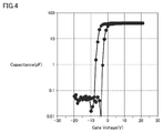
- FIG. 4 is a graph for explaining the width of the variable capacitance of the variable capacitance element 100 according to the first embodiment.
- the width of the capacitance that the variable capacitance element 100 can change depends on the capacitance of the second capacitor as described above. That is, the wider the portion C2 where the drain electrode 6 and the terminal electrode 22 overlap in a plan view, the larger the capacity of the second capacitor, and the wider the width of the capacity that the variable capacitance element 100 can change.
- the area of the portion C2 where the drain electrode 6 and the terminal electrode 22 overlap in a plan view is 1000 times the area of the portion C1 in which the source electrode 5 and the terminal electrode 22 overlap in a plan view (area ratio 1000). It is an actually measured value of the variable capacitance element 100 which was doubled).
- the horizontal axis is the applied voltage of the gate electrode 2 (unit is V), and the vertical axis is the capacity of the variable capacitance element 100 (unit is pF).
- variable capacitance element 100 designed so that the capacitance of only the first capacitor is 0.048 pF and the capacitance of the first capacitor and the second capacitor is 48 pF is actually measured, the applied voltage of the gate electrode 2 is less than the threshold value as shown in FIG.
- the capacity in the case of was 0.052 pF, and the capacity in the case of the threshold value or more was 41 pF.
- FIG. 5 is a cross-sectional view for explaining a method of manufacturing a variable capacitance element according to the first embodiment.
- a platinum (Pt) gate electrode 2 having a film thickness of 80 nm is formed on the (100) surface of the prepared semiconductor substrate 1 of lanthanum aluminate (LAO).
- LAO lanthanum aluminate
- the gate electrode 2 forms a photoresist with a predetermined pattern on the (100) surface of the semiconductor substrate 1 using a photolithography technique, and then forms platinum (Pt) by high-frequency (RF) sputtering. It is formed by removing the photoresist at lift-off.
- RF high-frequency
- the gate insulating film 3 having a film thickness of 70 nm is formed by superimposing the gate electrode 2 on the surface of the semiconductor substrate 1 on which the gate electrode 2 is formed.
- the gate insulating film 3 is formed by spin-coating a La-HfO 2 solution on the surface of the semiconductor substrate 1 on which the gate electrode 2 is formed by using a chemical solution deposition method (CSD) (CSD). It is formed by drying at ° C. and then firing at 800 ° C. to crystallize in an oxygen atmosphere.
- CSD chemical solution deposition method
- a channel forming film 4 having a film thickness of 25 nm is formed by superimposing the gate insulating film 3 on the gate insulating film 3.
- the channel forming film 4 is formed by spin-coating an IZO solution on the gate insulating film 3 using a chemical solution deposition method (CSD), drying at 150 ° C., and then under an oxygen atmosphere. It is formed by firing at 500 ° C. and crystallizing.
- CSD chemical solution deposition method
- a platinum (Pt) source electrode 5 and a drain electrode 6 having a film thickness of 80 nm are formed on the channel forming film 4.
- the source electrode 5 and the drain electrode 6 form a photoresist of a predetermined pattern on the channel forming film 4 by using a photolithography technique, and then platinum (Pt) is formed by high frequency (RF) sputtering. It is formed by forming a film and removing the photoresist by lift-off.
- RF high frequency
- a dielectric 21 is formed on the source electrode 5 and the drain electrode 6 with an Al2O3 film having a film thickness of 500 nm. Specifically, the dielectric 21 forms a photoresist of a predetermined pattern on the source electrode 5 and the drain electrode 6 by using a photolithography technique, and then an Al 2 O 3 film is subjected to ECR (Electron Cyclotron Resonance) sputtering. Is formed by forming a film and removing the photoresist by lift-off.
- ECR Electro Cyclotron Resonance
- a platinum (Pt) terminal electrode 22 having a film thickness of 80 nm is formed on the dielectric 21.
- the terminal electrode 22 forms a photoresist of a predetermined pattern on the dielectric 21 using a photolithography technique, and then forms platinum (Pt) by high frequency (RF) sputtering to lift off. It is formed by removing the photoresist with.
- variable capacitance element 100 As the variable capacitance element 100 described so far, an element whose capacitance is variable by two values of the capacitance of only the first capacitor and the combined capacitance of the first capacitor and the second capacitor has been described. However, by forming a plurality of variable capacitance elements 100 in a matrix on the semiconductor substrate 1, a multivalued variable capacitance element can be configured.
- FIG. 6 is a circuit diagram of the multi-valued variable capacitance element 100a according to the first embodiment.
- variable electronic elements such as inductors and registers other than the capacitor as the included passive elements in a matrix, it is possible to similarly configure a multi-valued variable electronic element.
- FIG. 6 shows a circuit diagram of a variable capacitance element 100a in which one variable capacitance element 100 shown in FIG. 3 is connected in a matrix of n ⁇ n.
- the terminal 22a of the terminal electrode 5a (first terminal electrode) and the terminal electrode 22 (second terminal electrode) is common to n ⁇ n variable capacitance elements 100.
- each control electrode terminal 2a of the n ⁇ n variable capacitance elements 100 is provided separately, and is shown in the terminal G11 to the terminal Gnn and FIG.
- variable capacitance element 100 the configuration in which the element unit 20 is provided above the switch unit 10 as shown in FIG. 1 has been described, but the element unit 20 may be provided below the switch unit 10. Specifically, a variable capacitance element in which the element unit 20 is provided under the switch unit 10 will be described.
- FIG. 7 is a cross-sectional view for explaining the configuration of the variable capacitance elements 100b and 100c according to the modified example of the first embodiment.
- the same components as those of the variable capacitance element 100 shown in FIG. 1 are designated by the same reference numerals, and detailed description thereof will not be repeated.
- FIG. 7A is a variable capacitance element 100b using a multilayer ceramic capacitor (MLCC: multi-layer ceramic capacitor) in the element unit 20b.
- MLCC multi-layer ceramic capacitor
- a source electrode 5 and a drain electrode 6 are formed on the upper surface of the laminated ceramic capacitor of the element portion 20b, and a channel forming film 4, a gate insulating film 3, and a gate electrode 2 are formed on the source electrode 5 and the drain electrode 6 in this order to form a switch portion. It constitutes 10.
- the multilayer ceramic capacitor of the element portion 20b includes a portion of the first capacitor connected to the source electrode 5 and a portion of the second capacitor connected to the drain electrode 6.
- the first capacitor portion includes a plurality of electrodes 25b connected to the source electrode 5 and electrodes 24b connected to the terminal electrode 22b which is an external electrode of the laminated ceramic capacitor, for example, sandwiching a dielectric 21b of barium titanate. It is a laminated structure.
- the portion of the second capacitor has a configuration in which a plurality of electrodes 23b connected to the drain electrode 6 and electrodes 24b connected to the terminal electrode 22b are laminated with the dielectric 21b interposed therebetween.
- variable capacitance element 100b Similar to the variable capacitance element 100, the variable capacitance element 100b has a channel forming film 4 that overlaps with the gate electrode 2 in a plan view because a gate voltage equal to or higher than the threshold value is not applied to the gate electrode 2 when the switch unit 10 is in the OFF state. There is an electron depletion layer at the position, and the source electrode 5 and the drain electrode 6 do not conduct with each other. Therefore, the variable capacitance element 100b has the capacitance of only the first capacitor because the voltage is applied only to the dielectric 21b between the electrode 25b connected to the source electrode 5 and the electrode 24b connected to the terminal electrode 22b. ..
- variable capacitance element 100b when the switch unit 10 is in the ON state, a channel is formed by applying a gate voltage equal to or higher than the threshold value to the gate electrode 2, and the source electrode 5 and the drain electrode 6 are made conductive. Therefore, in the variable capacitor element 100b, a voltage is applied to the dielectric 21b between the electrode 25b connected to the source electrode 5 and the electrode 23b connected to the drain electrode 6 and the electrode 24b connected to the terminal electrode 22b. Therefore, it becomes the combined capacitance of the first capacitor and the second capacitor.
- LTCC Low Temperature Co-fired Ceramics
- HTCC High Temperature Co-Fired Ceramics
- FIG. 7B is a variable capacitance element 100c using a silicon capacitor for the element unit 20c.
- a source electrode 5 and a drain electrode 6 are formed on the upper surface of the silicon capacitor of the element portion 20c, and a channel forming film 4, a gate insulating film 3, and a gate electrode 2 are formed on the source electrode 5 and the drain electrode 6 in this order, and the switch portion 10 is formed. Consists of.
- the silicon capacitor of the element portion 20c is formed on the surface of the N + layer 24c formed by injecting n-type impurity ions into the silicon substrate 1a, the dielectric 21c formed on the surface thereof, and the dielectric 21c formed by the semiconductor process. It is composed of a polysilicon layer 25c formed and connected to the source electrode 5 or a polysilicon layer 23c connected to the drain electrode 6.
- the dielectric 21c is made of, for example, an inorganic material formed by a CVD (Chemical Vapor Deposition) method or the like, such as silicon oxide, silicon nitride, hafnium oxide, hafnium silicate, alumina, and barium titanate. It should be noted that a plurality of trenches or a plurality of pillars are formed on the silicon substrate 1a to form an uneven shape.
- the silicon capacitor of the element portion 20c includes a portion of the first capacitor connected to the source electrode 5 and a portion of the second capacitor connected to the drain electrode 6.
- the portion of the first capacitor is composed of a portion of the dielectric 21c sandwiched between the polysilicon layer 25c connected to the source electrode 5 and the N + layer 24c connected to the terminal electrode 22c.
- the portion of the second capacitor is composed of a portion of the dielectric 21c sandwiched between the polysilicon layer 23c connected to the drain electrode 6 and the N + layer 24c connected to the terminal electrode 22c.
- variable capacitance element 100c Similar to the variable capacitance element 100, the variable capacitance element 100c has a channel forming film 4 that overlaps with the gate electrode 2 in a plan view because a gate voltage equal to or higher than the threshold value is not applied to the gate electrode 2 when the switch unit 10 is in the OFF state. There is an electron depletion layer at the position, and the source electrode 5 and the drain electrode 6 do not conduct with each other. Therefore, in the variable capacitor element 100c, a voltage is applied only to the portion of the dielectric 21c sandwiched between the polysilicon layer 25c connected to the source electrode 5 and the N + layer 24c connected to the terminal electrode 22c. Therefore, the capacity is only the first capacitor.
- variable capacitance element 100c when the switch unit 10 is in the ON state, a channel is formed by applying a gate voltage equal to or higher than the threshold value to the gate electrode 2, and the source electrode 5 and the drain electrode 6 are made conductive. Therefore, the variable capacitor element 100c is sandwiched between the polysilicon layer 25c connected to the source electrode 5 and the polysilicon layer 23c connected to the drain electrode 6 and the N + layer 24c connected to the terminal electrode 22c. Since a voltage is applied to the portion of the dielectric 21c, it becomes the combined capacitance of the first capacitor and the second capacitor.
- the capacity of the element portion 20c is increased by providing an uneven portion on the silicon substrate 1a, but if the required capacity can be secured, the dielectric 21c is a parallel flat plate. It may be in the shape of.
- variable capacitance element 100 includes a switch unit 10 constituting a field effect transistor and an element unit 20 electrically connected to the switch unit 10 to form a capacitor (passive element). , Is equipped.
- the switch portion 10 is formed by superimposing the source electrode 5, the drain electrode 6, the channel forming film 4 formed by superimposing at least a part of the source electrode 5 and a part of the drain electrode 6, and the channel forming film 4. It has a gate insulating film 3 formed therein and a gate electrode 2 formed so as to be superimposed on the gate insulating film 3.
- the element unit 20 constitutes a first capacitor (first passive element) between the terminal electrode 5a (first terminal electrode) electrically connected to the source electrode 5 and the source electrode 5, and at least the drain electrode 6 It has a terminal electrode 22 (second terminal electrode) constituting a second capacitor (second passive element). Therefore, the variable capacitance element 100 has a case where the element unit 20 is configured by the first capacitor and a case where the element unit 20 is configured by the first capacitor and the second capacitor by operating the switch unit 10 ON / OFF. It can be switched and the capacity of the capacitor can be changed.
- the switch unit 10 is preferably provided at the upper part or the lower part of the element unit 20.
- variable capacitance element 100 forms a first capacitor between the source electrode 5 and the terminal electrode 22, and a second capacitor between the drain electrode 6 and the terminal electrode 22. Therefore, the width in which the capacitance of the capacitor can be varied can be widened, and a sufficient withstand voltage can be obtained without reducing the capacitance of the capacitor.
- the element unit 20 further has a dielectric 21 provided on the source electrode 5 and the drain electrode 6, and is a first passive element in the dielectric 21 between the source electrode 5 and the terminal electrode 22. It is preferable to form a capacitor, and at least a second capacitor to be a second passive element is formed of a dielectric 21 between the drain electrode 6 and the terminal electrode 22.
- the gate electrode 2 is formed on the semiconductor substrate 1, the gate insulating film 3 is formed on the gate electrode 2 and the semiconductor substrate 1, the channel forming film 4 is formed on the gate insulating film 3, and the source electrode is formed. It is preferable that the 5 and the drain electrode 6 are formed on the channel forming film 4, the dielectric 21 is formed on the source electrode 5 and the drain electrode 6, and the terminal electrode 22 is formed on the dielectric 21.
- the passive element included is a capacitor, and the variable capacitance element capable of varying the capacitance has been described, but the included passive element is not limited to the capacitor.
- the passive element included is an inductor, and a variable inductance element capable of varying the inductance will be described with reference to the drawings.
- FIG. 8 is a cross-sectional view for explaining the configuration of the variable inductance element 200 according to the second embodiment.
- FIG. 9 is a circuit diagram of the variable inductance element 200 according to the second embodiment.
- the same components as those of the variable capacitance element 100 shown in FIGS. 1 and 3 are designated by the same reference numerals, and detailed description thereof will not be repeated.
- the variable inductance element 200 shown in FIG. 8 includes a switch unit 10 constituting a field effect transistor and an element unit 20A electrically connected to the switch unit 10 and constituting a passive element.
- the element unit 20A is provided at the lower part of the switch unit 10.
- the switch unit 10 has a gate electrode 2, a gate insulating film 3, a channel forming film 4, a source electrode 5, and a drain electrode 6.
- a source electrode 5 and a drain electrode 6 are formed on the upper surface of the element unit 20A, and a channel forming film 4, a gate insulating film 3, and a gate electrode 2 are formed on the source electrode 5 and the drain electrode 6 in this order. Consists of.
- the element portion 20A is an inductor, and includes a portion of the first inductor connected to the source electrode 5 and a portion of the second inductor connected to the drain electrode 6.
- the portion of the first inductor is composed of a coil electrode 23 connected to a source electrode 5 and a terminal electrode 22A which is an external electrode of the inductor.
- the portion of the second inductor is composed of a coil electrode 24 connected to the drain electrode 6 and the terminal electrode 22A which is an external electrode of the inductor.
- the coil electrode 23 and the coil electrode 24 are formed in the same non-magnetic ceramics 25.
- the source electrode 5 itself may be used as the terminal electrode 5a.
- the control electrode terminal 2a is provided on the gate electrode 2 shown in FIG. 8
- the gate electrode 2 itself may be used as the control electrode terminal 2a.
- the terminal 22a of the terminal electrode 22A is provided on the terminal electrode 22A shown in FIG. 8, the terminal electrode 22A itself may be used as the terminal 22a.
- variable inductance element 200 Similar to the variable capacitance element 100, the variable inductance element 200 has a channel forming film 4 that overlaps with the gate electrode 2 in a plan view because a gate voltage equal to or higher than the threshold value is not applied to the gate electrode 2 when the switch unit 10 is in the OFF state. There is an electron depletion layer at the position, and the source electrode 5 and the drain electrode 6 do not conduct with each other. Therefore, in the variable inductance element 200, the current flows only in the coil electrode 24 between the source electrode 5 and the terminal electrode 22A, so that the inductance is only for the first inductor.
- variable inductance element 200 when the switch unit 10 is in the ON state, a channel is formed by applying a gate voltage equal to or higher than the threshold value to the gate electrode 2, and the source electrode 5 and the drain electrode 6 are made conductive. Therefore, in the variable inductance element 200, a current flows between the coil electrode 23 between the source electrode 5 and the terminal electrode 22A and the coil electrode 24 between the drain electrode 6 and the terminal electrode 22A, so that the first inductor and the second inductor and the second inductor It is the combined inductance of the inductor.
- variable inductance element 200 has a terminal electrode 5a (first terminal electrode) and a terminal 22a of the terminal electrode 22A (second terminal electrode) connected to a converter circuit or the like.
- the control electrode terminal 2a for varying the inductance is connected to a circuit different from the converter circuit. Therefore, it is unlikely that the signal applied to the control electrode terminal 2a is affected by the signal of the converter circuit.
- the passive element is an inductor
- the element portion 20A is electrically connected between the source electrode 5 and the terminal electrode 22A. It has a first inductor that becomes a passive element and a second inductor that is electrically connected between the drain electrode 6 and the terminal electrode 22A and becomes a second passive element.
- variable inductance element 200 constitutes a first inductor between the source electrode 5 and the terminal electrode 22A, and a second inductor between the drain electrode 6 and the terminal electrode 22A. Therefore, the width in which the inductance of the inductor can be varied can be widened, and a sufficient withstand voltage can be obtained without reducing the inductance of the inductor.
- a multi-valued variable inductance element may be configured by forming a plurality of variable inductance elements 200 in a matrix. Further, by changing the coil electrodes 23 and 24 shown in FIG. 8 to resistance elements, the passive element may be used as a register and may be used as a variable register element. Further, the configuration of the switch unit 10 described in the first and second embodiments is not limited to the described configuration, and may be, for example, a silicon MOSFET or a GaN FET.
- variable capacitance elements 100, 100a and the variable inductance element 200 can have a wide range in which the physical quantity of the passive element can be changed due to their configurations, and the passive element can have a wide range. It has the property that a sufficient withstand voltage can be obtained without reducing the physical quantity.
- a circuit device including the variable capacitance elements 100 and 100a and the variable inductance element 200 that utilize this characteristic will be described below.
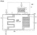
- FIG. 10 is a circuit diagram of the circuit device according to the third embodiment.
- FIG. 10B is an equivalent circuit of FIG. 10A.
- the circuit device 300 shown in FIG. 10A is a circuit that adjusts the output level according to the load fluctuation, and is an LLC resonance converter.
- the circuit device 300 which is an LLC resonance converter, can convert the input voltage Vin into the output voltage Vout.
- the circuit device 300 includes switching elements Q1 and Q2, a transformer T, a resonance capacitor Cr, a leakage inductor Lr, Lr1, Lr2, an exciting inductor Lm, output rectifying diodes D1 and D2, and an output capacitor C0.
- the output capacitor C0 is connected to the load resistance R0.
- ) of the circuit device 300 which is an LLC resonance converter, can be expressed as (Equation 1).
- the input / output voltage ratio of the LLC resonance converter can be adjusted by modulating the switching frequency f of the switching elements Q1 and Q2. Then, the LLC resonance converter is usually operated at a frequency higher than the maximum value of the input / output voltage ratio, and the output voltage (Vout) of the LLC resonance converter is adjusted by changing the switching frequency according to the load fluctuation. ..
- the LLC resonance converter when lowering the output voltage (Vout), the LLC resonance converter needs to have a switching frequency higher than the frequency at which the input / output voltage ratio becomes the maximum value.
- the power loss of the LLC resonance converter depends on the switching frequency, there is a problem that the power loss increases when the switching frequency is increased and the output voltage (Vout) of the LLC resonance converter is lowered.
- the variable capacitance element 100 of the first embodiment is used for the resonance capacitor Cr.
- the output voltage (Vout) can be lowered without increasing the switching frequency by using the resonance capacitor Cr as the variable capacitance element 100.
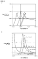
- FIG. 11 is a graph for explaining the frequency characteristics of the circuit device 300 according to the third embodiment.
- FIG. 11A shows the frequency characteristics of the input / output voltage ratio when the capacitance is 1.5 times, 10 times, and 100 times the capacitance of the resonance capacitor Cr (for example, 0.02 ⁇ F).
- .. 11 (b) is an enlarged view of a part of the graph of FIG. 11 (a).
- the horizontal axis is the operating frequency (unit: Hz)
- the vertical axis is the input / output voltage ratio.
- the frequency characteristic of the input / output voltage ratio when the capacitance of the resonance capacitor Cr is multiplied by 100 is Graph A, and the capacitance of the resonance capacitor Cr is multiplied by 10. It is a graph B. Further, in FIGS. 11 (a) and 11 (b), the frequency characteristic of the input / output voltage ratio when the capacitance of the resonance capacitor Cr is multiplied by 1.5 is the same as that of Graph C and the capacitance of the resonance capacitor Cr. The case where this is done is the graph D.
- the input / output voltage ratio of the graph D is
- 4.0
- the input / output voltage ratio of the graph C is
- 2.2.
- the input / output voltage ratio of the graph B is
- 0.9
- the input / output voltage ratio of the graph A 0.8. That is, by varying the capacitance of the resonance capacitor Cr by about 10 times, the input / output voltage ratio can be changed in the range of 4.0 to 0.9 without changing the operating frequency.
- variable capacitance element 100 for the resonance capacitor Cr of the circuit device 300 the output voltage (Vout) can be lowered without increasing the power loss.
- the capacitance of the resonance capacitor Cr can be dynamically changed, and the input / output voltage ratio can be changed in multiple stages. Can be done.
- the LLC resonance converter has a circuit configuration using LC resonance, and low-loss soft switching can be realized by the circuit configuration.
- the variable capacitance element 100 for the resonance capacitor Cr for example, for a switching amplifier (such as a PWM (Pulse Width Modulation) amplifier), the capacitance of the resonance capacitor Cr can be dynamically changed during switching. The loss can be greatly reduced.
- FIG. 12 is a block diagram of the circuit device according to the fourth embodiment.
- the circuit device shown in FIG. 12 is a switching amplifier, and an LLC resonance converter having a resonance capacitor Cr as a variable capacitance element 100 is used in the class D output stage 301 thereof.
- the capacitance value of the resonance capacitor Cr variable capacitance element 100
- the capacitive impedance after the class D output stage 301 is reduced and low loss soft switching is realized. can.
- FIG. 13 is a timing chart showing the switching timing of the circuit device according to the fourth embodiment.
- the LLC resonance converter the voltage and current are vibrated at the LC resonance frequency, so that the PWM is turned on (ZVS: Zero Voltage Switching) when the voltage V DS is zero as shown in FIG. 13 (b). It is possible. Further, in the LLC resonance converter, by vibrating the voltage and the current at the LC resonance frequency, it is possible to turn on the PWM (ZCS: Zero Current Switching) in the state where the current ID is zero. Therefore, in the LLC resonance converter, the switching loss can be reduced. Switching as shown in FIG. 13B is called soft switching.
- the LLC resonance converter (circuit device 300) as shown in FIG. 10 has a resonance frequency fr of the resonance capacitor Cr and the leakage inductor Lr, and a resonance frequency fm of the resonance capacitor Cr, the leakage inductor Lr, and the excitation inductor Lm. It has two resonance frequencies.
- the condition for establishing the soft switching state is determined by the relationship between the resonance frequencies fr and fm and the switching frequency f. For example, when the switching frequency f is smaller than the resonance frequency fm (f ⁇ fm), the circuit device 300 satisfies the hard switching condition. However, it is a condition that is not normally used because gain inversion occurs.
- the conditions under which the soft switching state is established differ depending on the load conditions, and are determined by the conditional expressions shown in (Equation 4) and (Equation 5).
- the condition for establishing soft switching changes depending on the fluctuation of the voltage Vcr of the Vin or the resonance capacitor Cr, so that the circuit device 300 has a condition for increasing the switching loss.
- the voltage Vcr fluctuates depending on the load condition and the capacitance of the resonance capacitor Cr. Therefore, in the circuit device 300, by using the variable capacitance element 100 for the resonance capacitor Cr to change the capacitance, it is possible to control the condition under the condition that soft switching is established.
- variable capacitance element 100 is used for the resonance capacitor Cr.
- the variable capacitance element 100 has a wider range in which the capacitance can be changed as compared with the conventional variable capacitance element, so that it is possible to cope with a large fluctuation of the input voltage Vin and the load condition. ..
- variable capacitance element 100 for the resonance capacitor Cr of the circuit device 300 the capacitance of the resonance capacitor Cr can be greatly varied, and the conditions for establishing soft switching can be widely secured.
- the capacitance of the resonance capacitor Cr can be dynamically changed, and the conditions under which soft switching is established can be adjusted in multiple steps. Can be done with.
- the circuit device capable of adjusting the condition for establishing soft switching by varying the resonance capacitor Cr or the like is not limited to the circuit device 300 which is an LLC resonance converter, and is not limited to a current resonance circuit, a voltage resonance circuit, or a plurality of circuits. It can also be applied to various resonance type circuit devices such as a resonance circuit, a series resonance circuit, and a parallel resonance circuit.
- circuit blocks for multiple frequencies to reduce the circuit scale and the number of parts.
- the circuit blocks are shared for a plurality of frequencies, it is necessary to suppress signal reflection between the circuit blocks, and it is necessary to perform impedance matching according to each frequency.
- the capacitance value of the capacitor is changed in order to perform impedance matching and modulation of the resonance frequency, it is possible to cover a plurality of frequency bands while reducing the circuit scale and the number of parts.
- variable capacitance element 100 described in the first embodiment can have a wider range of variable capacitance than the conventional variable capacitance element. Therefore, the wireless communication terminal using the variable capacitance element 100 can cover a wide frequency band. Further, since the capacitance value of the variable capacitance element 100 is switched by the voltage applied to the control electrode terminal 2a, the capacitance value does not change non-linearly (gradually) with respect to the voltage unlike the conventional variable capacitance element. Therefore, in the wireless communication terminal using the variable capacitance element 100, the distortion signal is not generated, and the interference signal is not generated for other frequencies.
- FIG. 14 is a block diagram of the circuit device 400 according to the fifth embodiment.
- the circuit device 400 is a communication circuit block provided in a wireless communication terminal, and can be shared for a plurality of frequencies. Therefore, in the circuit device 400, the variable capacitance element 100 is applied to a capacitor that needs to have a variable capacitance value in order to perform impedance matching and modulation of the resonance frequency.
- variable capacitance element 100 can change the capacitance in the range of 10 times to 1000 times, impedance matching and modulation of the resonance frequency can be performed in a wider range, and a wider reception frequency band can be obtained. Can be covered. Further, in the circuit device 400, since the variable capacitance element 100 digitally changes the capacitance, the strain signal can be suppressed. Therefore, by using the circuit device 400, it is possible to realize a multi-band wireless communication terminal capable of covering a plurality of frequency bands while reducing the circuit scale and the number of parts.
- a multi-valued variable capacitance element 100a may be used for the capacitor of the circuit device 400.
- the configuration of the DC circuit breaker can be similarly applied to switches, connecting devices, and arc suppression devices of various power supply circuits. Further, the DC circuit breaker can be used, for example, in an energy harvesting device such as solar power generation, a fuel cell, a lithium ion battery, or the like.
- FIG. 15 is a circuit diagram of the circuit device 500 according to the sixth embodiment.
- the circuit device 500 is a hybrid switch circuit used for a DC circuit breaker, and has a metal contact S1 and a MOSFET semiconductor switch S2.
- the metal contact S1 can be opened and closed without arc discharge, there is an advantage that the contact is not consumed, the life is long, high-speed current can be cut off, and noise due to arc discharge is not generated.
- FIG. 16 is a graph for explaining the switching characteristics of the circuit device 500 according to the sixth embodiment.
- the horizontal axis is time t and the vertical axis is the recurrence voltage V.
- the recurrence voltage V of the metal contact S1 increases linearly with respect to time t.
- the recurrence voltage V of the metal contact S1 rises as steeply as possible after the metal contact S1 is turned off.
- the circuit loss can be reduced by steeply increasing the recurrence voltage V of the metal contact S1.
- the capacity of the capacitor C is set to a relatively large capacity (for example, several tens of nF) in order to absorb the charge that generates an arc discharge. You need to keep it.
- variable capacitance element described in the first embodiment is used for the capacitor C, and the capacitance of the capacitor C is greatly varied between when the metal contact S1 is ON and OFF. I am trying to do it. Therefore, the circuit device 500 realizes a DC circuit breaker having a very low circuit loss while suppressing arc discharge.
- variable capacitance element described in the first embodiment it is possible to obtain a high withstand voltage while varying the capacitance in a wide range, which was difficult to realize with the conventional variable capacitance element.
- a multi-valued variable capacitance element 100a may be used for the capacitor C of the circuit device 500.
- the switch unit 10 has a gate electrode 2, a gate insulating film 3, a channel forming film 4, a source electrode 5, and a drain electrode 6.
- the drain electrode 6 is a floating electrode, and it is possible to form a switch portion in which the drain electrode 6 is not provided.
- FIG. 17 is a cross-sectional view for explaining the configuration of the variable capacitance element 100d according to the seventh embodiment.
- FIG. 18 is a plan view for explaining the configuration of the variable capacitance element 100d according to the seventh embodiment.
- the same components as those of the variable capacitance element 100 shown in FIGS. 1 and 2 are designated by the same reference numerals, and detailed description thereof will not be repeated.
- the variable capacitance element 100d shown in FIG. 17 includes a switch unit 10d formed on the semiconductor substrate 1 and constituting a field effect transistor, and an element unit 20 electrically connected to the switch unit 10d and constituting a passive element. There is.
- the element unit 20 is provided above the switch unit 10d.
- the switch unit 10d has a gate electrode 2d, a gate insulating film 3, a channel forming film 4, and a source electrode 5.
- the gate electrode 2d is formed on the semiconductor substrate 1
- the gate insulating film 3 and the channel forming film 4 are sequentially formed on the gate electrode 2d
- the source electrode 5 is formed on them. are doing.
- the gate electrode 2d is widened as shown in FIG. 18, and most of the terminal electrode 22 overlaps with the gate electrode 2d in a plan view. Therefore, in the variable capacitance element 100d, when the switch portion 10d is turned on, a gate voltage is applied to the gate electrode 2d, and a channel charge is generated in the portion of the channel forming film 4 that overlaps the gate electrode 2d in a plan view. In the variable capacitance element 100d, a voltage is applied between the portion of the source electrode 5 and the channel forming film 4 and the terminal electrode 22 facing the portion to form a capacitance.
- variable capacitance element 100d when the switch unit 10d is in the OFF state, the variable capacitance element 100d does not generate a channel charge on the channel forming film 4 because the gate voltage is not applied to the gate electrode 2d. Therefore, since the voltage is applied only between the source electrode 5 and the terminal electrode 22 facing the source electrode 5, the variable capacitance element 100d has the capacitance of only the first capacitor.
- the element unit 20 constitutes a first capacitor (first passive element) between the source electrode 5 and the terminal electrode 22, and a second capacitor (second passive element) between the gate electrode 2d and the terminal electrode 22. ).
- first capacitor is a portion C1 in which the source electrode 5 and the terminal electrode 22 overlap in a plan view.
- the second capacitor is a portion C3 in which the gate electrode 2d and the terminal electrode 22 overlap in a plan view.
- variable capacitance element 100d Even with the variable capacitance element 100d, there are cases where the first capacitor element is the element unit 20 and the case where the first capacitor element and the second capacitor element are the element unit 20 by operating the switch unit 10d ON / OFF. It can be switched and the capacity of the capacitor can be changed. Even with the variable capacitance element 100d, the switch unit 10d that operates ON / OFF by the voltage applied to the gate electrode 2d (control electrode terminal 2a), the terminal electrode 5a (first terminal electrode), and the terminal electrode 22 (second terminal electrode 22). It is a variable capacitance element that operates at three terminals separately from the element unit 20 that operates at the terminal electrode).
- variable capacitance element 100d since the capacitance of the second capacitor element can be changed by the channel charge generated in the channel forming film 4 without providing the drain electrode, the second capacitor element can be changed by the voltage applied to the gate electrode 2d.
- the capacity of is continuously variable.
- the residual charge to the floating electrode is reduced during the ON / OFF operation of the switch unit 10d by not providing the drain electrode which is a floating electrode, so that the potential of the capacitor is stabilized. It is possible to reduce the risk of failure due to short circuit or short circuit.
- variable capacitor element 100d the conductivity can be changed stepwise in a wide region of the channel forming film 4 according to the level of the gate voltage to be applied by adopting a configuration in which the drain electrode which is a floating electrode is not provided.
- the capacitance of the capacitor can be changed more continuously.
- variable capacitance element 100d uses the portion C3 in which the gate electrode 2d and the channel forming film 4 overlap in a plan view instead of the drain electrode.
- a second capacitor element is formed between the portion C3 and the terminal electrode 22. Thereby, the variable capacitance element 100d can continuously change the capacitance of the second capacitor element.
- variable capacitance element 100d the configuration in which the element unit 20 is provided above the switch unit 10d as shown in FIG. 17 has been described, but the element unit 20 may be provided below the switch unit 10d. Further, by forming a plurality of variable capacitance elements 100d in a matrix, a multi-valued variable electronic element may be similarly configured. Further, the configuration of the variable capacitance element 100d may be applied to variable electronic elements such as inductors and registers other than capacitors.
- the terminal electrode 22 is also formed on the upper part of the channel region formed between the source electrode 5 and the drain electrode 6. Therefore, the variable capacitance element 100 may affect the ON / OFF state of the switch unit 10 by the voltage applied to the terminal 22a of the terminal electrode 22. That is, in the variable capacitance element 100, the capacitance value may fluctuate depending on the signal between the terminal electrode 5a (first terminal electrode) and the terminal 22a of the terminal electrode 22 (second terminal electrode).
- FIG. 19 is a cross-sectional view for explaining the configuration of the variable capacitance element 100e according to the eighth embodiment.
- FIG. 20 is a plan view for explaining the configuration of the variable capacitance element 100e according to the eighth embodiment.
- the same components as those of the variable capacitance element 100 shown in FIGS. 1 and 2 are designated by the same reference numerals, and detailed description thereof will not be repeated.
- the variable capacitance element 100e shown in FIG. 19 includes a switch unit 10 forming a field effect transistor formed on the semiconductor substrate 1 and an element unit 20e electrically connected to the switch unit 10 and constituting a passive element. There is.
- the element unit 20e is provided on the upper portion of the switch unit 10.
- the element unit 20e includes an Al 2 O 3 film of the dielectric 21 and a platinum (Pt) terminal electrode 22e (second terminal electrode) formed over the dielectric 21.
- the terminal electrode 22e is formed in a pattern avoiding the channel region formed between the source electrode 5 and the drain electrode 6. Therefore, in the cross-sectional view shown in FIG. 19, the terminal electrode 22e1 formed on the upper part of the source electrode 5 and the terminal electrode 22e2 formed on the upper part of the drain electrode 6 are shown separately.
- the element unit 20e constitutes a first capacitor (first passive element) between the source electrode 5 and the terminal electrode 22e1, and a second capacitor (second passive element) between the drain electrode 6 and the terminal electrode 22e2.
- first capacitor is a portion C1 in which the source electrode 5 and the terminal electrode 22e1 overlap in a plan view.
- the second capacitor is a portion C4 in which the drain electrode 6 and the terminal electrode 22e2 overlap in a plan view.
- variable capacitance element 100e when the switch unit 10 is in the OFF state, a gate voltage equal to or higher than the threshold value is not applied to the gate electrode 2, so that there is an electron depletion layer at the position of the channel forming film 4 overlapping the gate electrode 2 in a plan view.
- the source electrode 5 and the drain electrode 6 do not conduct with each other. Therefore, since the voltage is applied only between the source electrode 5 and the portion (first region) of the terminal electrode 22e1 facing the source electrode 5, the variable capacitance element 100e has the capacitance of only the first capacitor.
- variable capacitance element 100e when the switch unit 10 is in the ON state, a channel is formed by applying a gate voltage equal to or higher than the threshold value to the gate electrode 2, and the source electrode 5 and the drain electrode 6 are made conductive. Therefore, in the variable capacitance element 100e, a voltage is applied between the source electrode 5 and the drain electrode 6 and the opposite terminal electrode 22e (first region + second region), so that the first capacitor and the second capacitor have different voltages. It becomes the combined capacity.
- the portion of the terminal electrode 22e that overlaps the source electrode 5 in a plan view is referred to as a first region (terminal electrode 22e1)
- the portion that overlaps the drain electrode in a plan view is referred to as a second region (terminal electrode 22e2).
- the switch unit 10 has a switch portion 10 as compared with the variable capacitance element 100 shown in FIG.
- the capacity in the ON state becomes small.
- the capacitance value is less likely to fluctuate due to the signal between the terminal electrode 5a (first terminal electrode) and the terminal 22a of the terminal electrode 22 (second terminal electrode).
- the variable capacitance element 100e as shown in FIG. 20, even if the terminal electrode 22e is not formed in a pattern that bypasses all parts of the channel region formed between the source electrode 5 and the drain electrode 6. Even in a pattern that overlaps a part of the channel region, it is possible to suppress fluctuations in the capacitance value due to a signal between the first terminal electrode and the second terminal electrode.
- variable capacitance element 100e has a first region in which the terminal electrode 22e overlaps the source electrode 5 in a plan view and a second region in which the drain electrode 6 overlaps in a plan view, and the first region and the first region.
- the two regions are electrically connected by bypassing at least one part of the channel region formed between the source electrode 5 and the drain electrode 6.
- the fact that the terminal electrode 22e bypasses at least one part of the channel region formed between the source electrode 5 and the drain electrode 6 means that the terminal electrode 22e has a portion that does not overlap with at least one part of the channel region in a plan view. be.
- variable capacitance element 100e the configuration in which the element unit 20e is provided above the switch unit 10 as shown in FIG. 19 has been described, but the element unit 20e may be provided below the switch unit 10. Further, by forming a plurality of variable capacitance elements 100e in a matrix, a multi-valued variable electronic element may be similarly configured. Further, the configuration of the variable capacitance element 100e may be applied to variable electronic elements such as inductors and registers other than capacitors.
- FIG. 21 is a cross-sectional view for explaining the configuration of the variable capacitance element 100f according to the modified example of the eighth embodiment.
- the same components as those of the variable capacitance element 100e shown in FIGS. 19 and 20 are designated by the same reference numerals, and detailed description thereof will not be repeated.
- the variable capacitance element 100f shown in FIG. 21 includes a switch unit 10 forming a field effect transistor formed on the semiconductor substrate 1 and an element unit 20f electrically connected to the switch unit 10 and constituting a passive element. There is.
- the element unit 20f is provided on the upper part of the switch unit 10.
- the element unit 20f includes an Al2O3 film of the dielectric 21f and a platinum (Pt) terminal electrode 22e (second terminal electrode) formed so as to be superimposed on the dielectric 21f.
- the terminal electrode 22e is formed in a pattern avoiding the channel region formed between the source electrode 5 and the drain electrode 6.
- the dielectric 21f is formed in a pattern that avoids the channel region formed between the source electrode 5 and the drain electrode 6 in accordance with the pattern of the terminal electrode 22e. Therefore, in the cross-sectional view shown in FIG. 21, the dielectric 21f1 and the terminal electrode 22e1 formed on the upper part of the source electrode 5 and the dielectric 21f2 and the terminal electrode 22e2 formed on the upper part of the drain electrode 6 are separated. Is illustrated.
- the dielectric 21f is aligned with the source electrode 5 in accordance with the pattern of the terminal electrode 22e. It is formed avoiding at least one part of the channel region formed between the drain electrode 6 and the drain electrode 6.
- ⁇ is each frequency. That is, the switching speed can be improved by reducing the parasitic resistance R and the capacitor C (parasitic capacitance).
- ⁇ is the resistivity peculiar to the material of the channel forming film 4
- L is the channel length
- W is the channel width
- t is the film thickness of the channel forming film 4.
- the parasitic resistance R depends on the value of the channel length L / channel width W. Therefore, the Q value can be improved by increasing the channel width W with respect to the channel length L. Since the switch unit 10 provides the source electrode 5 and the drain electrode 6 on the channel forming film 4 as shown in FIG. 2, the channel length L and the channel width W can be easily changed by the device design. ..
- the capacitor C (parasitic capacitance) corresponds to the capacitance of the gate insulating film 3 of the switch unit 10, is proportional to the relative permittivity of the gate insulating film 3, and is inversely proportional to the film thickness. Therefore, since the switch unit 10 has a structure separated from the element unit 20, the capacitor C (parasitic capacitance) can be adjusted individually.
- the channel length L is 10 ⁇ m
- the channel width W is 100 ⁇ m
- the parasitic resistance R is 1 k ⁇
- the capacitor C parasititic capacitance
- the Q value is 0 at 1 MHz. It becomes 0.02.
- the channel length L is miniaturized to 1 ⁇ m
- the channel width W is 1000 ⁇ m
- the film thickness of the gate insulating film 3 is 10 times (7000 ⁇ m)
- the relative permittivity of the gate insulating film 3 is 1/5 (40 to If it is set to about 50)
- the Q value becomes 100. Therefore, the switch unit 10 can be improved to a switching speed of 5000 times.
- the IZO film is used for the channel forming film 4, but this is an example, and another film such as an ITO film may be used. Further, in the above-described embodiment, it has been described that the La-HfO 2 film is used for the gate insulating film 3, but this is an example and another film such as the Ce-HfO 2 film may be used.
- the channel forming film 4 is formed on the lower side of the source electrode 5 and the drain electrode 6 as shown in FIG. 1 (top contact). Construction).
- the top contact structure is a structure in which the source electrode 5 and the drain electrode 6 are in contact with each other on the upper side of the channel forming film 4 when viewed from the gate electrode 2 side.
- the variable electronic device is not limited to this, and the variable electronic device may form, for example, the channel forming film 4 in the variable capacitance element 100 on the upper side of the source electrode 5 and the drain electrode 6 (bottom contact structure).
- the bottom contact structure is a structure in which the source electrode 5 and the drain electrode 6 are in contact with each other on the lower side of the channel forming film 4 when viewed from the gate electrode 2 side.
- the gate electrode 2 is formed on the semiconductor substrate 1 as shown in FIG. 1, and is superposed on the gate electrode 2 to form the gate insulating film 3 and the gate insulating film 3.
- a bottom gate structure is adopted in which the channel forming film 4 is formed in order, and the source electrode 5 and the drain electrode 6 are formed on them.
- the variable electronic element is not limited to this, and a top gate structure may be adopted.
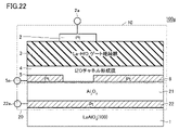
- FIG. 22 is a cross-sectional view for explaining the configuration of the variable capacitance element 100 g according to the modified example.
- the element unit 20 is provided at the lower part of the switch unit 10.
- the switch unit 10 forms a source electrode 5 and a drain electrode 6 on the dielectric 21, respectively, and superimposes the source electrode 5 and the drain electrode 6 on the channel forming film 4 and the gate insulating film 3 to form the gate insulating film 3 in order.
- a top gate structure in which the gate electrode 2 is formed on the gate electrode 2 is adopted.
- the variable capacitance element 100g shown in FIG. 22 the same components as those of the variable capacitance element 100 shown in FIG. 1 are designated by the same reference numerals, and detailed description thereof will not be repeated.
- variable capacitance element 100g having a top gate structure employs a top contact structure in which the source electrode 5 and the drain electrode 6 are in contact with each other on the upper side of the channel forming film 4 when viewed from the gate electrode 2 side.
- the present invention is not limited to this, and even with a variable capacitance element 100 g having a top gate structure, a bottom contact structure in which the source electrode 5 and the drain electrode 6 are in contact with each other under the channel forming film 4 when viewed from the gate electrode 2 side is provided. It may be adopted.
- the materials that can be used for the gate insulating film 3 and the dielectric 21 are listed below. Of course, the material is not limited to the following description.
- HfO 2 and HfO 2 are PbTiO 3 , a ferroelectric film obtained by doping HfO 2 with at least one of trivalent, tetravalent or pentavalent metal atoms such as Si, Ce, Y, Zr, Bi, Ni, Ta, and La.
- Ferroelectric material as a crystal, ferroelectric material with BaTiO 3 as a parent crystal, ferroelectric material having a Bi layered structure, other metal oxides having a perovskite type crystal, metal oxides having a pyrochlor type crystal, organic Ferroelectric materials and other resin materials (polykimide, acrylic, epoxy, polypropylene, polyester, polyethylene terephthalate, polyethylene naphthalate, polyphenylene sulfide, polylactic acid, and other materials that can be used for the channel forming film 4 are summarized below. Listed. Of course, the material is not limited to the following description.
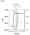
- the variable capacitance element 100 to 100 g has a memory characteristic derived from the configuration of the ferroelectric gate transistor. Specifically, in the variable capacitance element 100 shown in FIG. 1, the capacitance value C generated when an ON voltage (for example, + 10V) is applied to the gate electrode 2 to form a capacitor between the terminal electrode 22 and the drain electrode 6. On can be held by simply applying a holding voltage of 0 (zero) V or a small constant value (for example, ⁇ 1.0 V) to the gate electrode 2. Similarly, in the variable capacitance element 100, the capacitance value Coff that occurs when an OFF voltage (for example, -10V) is applied to the gate electrode 2 and a capacitor is not formed between the terminal electrode 22 and the drain electrode 6 is set to 0 (. It can be held by simply applying a holding voltage of zero) V or a small constant value (for example, ⁇ 1.0 V) to the gate electrode 2.
- FIG. 23 is a diagram for explaining the relationship between the capacitance of the variable capacitance element and the holding voltage.
- the horizontal axis is the gate voltage and the vertical axis is the capacitance.
- the terminal electrode is subjected to the gate voltage Vg applied to the gate electrode 2.
- the change in the capacitance value C that occurs between 22 and the drain electrode 6 becomes a hysteresis curve.
- FIG. 23 it can be seen that the capacitance value Con and the capacitance value Coff can be maintained by applying a holding voltage of ⁇ 1.0 V to the gate electrode 2.
- FIG. 24 is a diagram for explaining the relationship between the capacitance of the variable capacitance element and the holding time.
- the horizontal axis is time and the vertical axis is capacity.
- the capacitance value Con and the capacitance value Coff are changed for about 1.0 ⁇ 105 sec (27 hours) with a holding voltage of ⁇ 1.0 V applied to the gate electrode 2. Can be maintained without letting. Therefore, when a ferroelectric gate transistor configuration is adopted for the variable capacitance element 100 to 100 g, it is not necessary to apply a high gate voltage in order to maintain the capacitance, so that power can be saved and deterioration of the element can be suppressed. be able to.
Landscapes
- Engineering & Computer Science (AREA)
- Power Engineering (AREA)
- Microelectronics & Electronic Packaging (AREA)
- Manufacturing & Machinery (AREA)
- Semiconductor Integrated Circuits (AREA)
- Ceramic Capacitors (AREA)
- Fixed Capacitors And Capacitor Manufacturing Machines (AREA)
- Metal-Oxide And Bipolar Metal-Oxide Semiconductor Integrated Circuits (AREA)
- Thin Film Transistor (AREA)
- Filters And Equalizers (AREA)
Priority Applications (4)
| Application Number | Priority Date | Filing Date | Title |
|---|---|---|---|
| EP21879992.2A EP4187604A4 (en) | 2020-10-12 | 2021-10-08 | VARIABLE ELECTRONIC ELEMENT AND CIRCUIT DEVICE |
| JP2022556910A JP7569536B2 (ja) | 2020-10-12 | 2021-10-08 | 可変電子素子、および回路装置 |
| CN202180068716.3A CN116325039B (zh) | 2020-10-12 | 2021-10-08 | 可变电子元件以及电路装置 |
| US18/298,520 US20230246040A1 (en) | 2020-10-12 | 2023-04-11 | Variable electronic element and circuit device |
Applications Claiming Priority (2)
| Application Number | Priority Date | Filing Date | Title |
|---|---|---|---|
| JP2020-172070 | 2020-10-12 | ||
| JP2020172070 | 2020-10-12 |
Related Child Applications (1)
| Application Number | Title | Priority Date | Filing Date |
|---|---|---|---|
| US18/298,520 Continuation US20230246040A1 (en) | 2020-10-12 | 2023-04-11 | Variable electronic element and circuit device |
Publications (1)
| Publication Number | Publication Date |
|---|---|
| WO2022080253A1 true WO2022080253A1 (ja) | 2022-04-21 |
Family
ID=81208123
Family Applications (1)
| Application Number | Title | Priority Date | Filing Date |
|---|---|---|---|
| PCT/JP2021/037331 Ceased WO2022080253A1 (ja) | 2020-10-12 | 2021-10-08 | 可変電子素子、および回路装置 |
Country Status (5)
| Country | Link |
|---|---|
| US (1) | US20230246040A1 (https=) |
| EP (1) | EP4187604A4 (https=) |
| JP (1) | JP7569536B2 (https=) |
| CN (1) | CN116325039B (https=) |
| WO (1) | WO2022080253A1 (https=) |
Cited By (1)
| Publication number | Priority date | Publication date | Assignee | Title |
|---|---|---|---|---|
| WO2025142588A1 (ja) * | 2023-12-27 | 2025-07-03 | 株式会社村田製作所 | 発振器、およびその製造方法、情報処理装置 |
Citations (7)
| Publication number | Priority date | Publication date | Assignee | Title |
|---|---|---|---|---|
| JP2002373829A (ja) | 2001-06-15 | 2002-12-26 | Murata Mfg Co Ltd | 可変キャパシタ |
| US20040140528A1 (en) * | 2002-11-13 | 2004-07-22 | Kim Cheon Soo | Stacked variable inductor |
| JP2009147204A (ja) * | 2007-12-17 | 2009-07-02 | Taiyo Yuden Co Ltd | 可変キャパシタ |
| JP2010272815A (ja) * | 2009-05-25 | 2010-12-02 | Renesas Electronics Corp | 可変インダクタ |
| CN102570839A (zh) * | 2010-12-16 | 2012-07-11 | 西安高度电子科技有限公司 | 改变电容来改变谐振频率的llc谐振型dc-dc电源 |
| WO2018173497A1 (ja) * | 2017-03-22 | 2018-09-27 | ソニーセミコンダクタソリューションズ株式会社 | 半導体装置及びモジュール |
| WO2021205695A1 (ja) * | 2020-04-10 | 2021-10-14 | 株式会社村田製作所 | 可変容量素子及びそれを備えた発振器 |
Family Cites Families (8)
| Publication number | Priority date | Publication date | Assignee | Title |
|---|---|---|---|---|
| JPH0555474A (ja) * | 1991-08-23 | 1993-03-05 | Mitsubishi Electric Corp | 半導体装置 |
| DE10162263A1 (de) * | 2001-12-18 | 2003-07-10 | Infineon Technologies Ag | Induktives Bauteil |
| JP4939838B2 (ja) | 2005-05-31 | 2012-05-30 | 株式会社半導体エネルギー研究所 | 記憶装置 |
| US8837203B2 (en) | 2011-05-19 | 2014-09-16 | Semiconductor Energy Laboratory Co., Ltd. | Semiconductor device |
| JP6231735B2 (ja) | 2011-06-01 | 2017-11-15 | 株式会社半導体エネルギー研究所 | 半導体装置 |
| WO2013183472A1 (ja) * | 2012-06-08 | 2013-12-12 | 株式会社村田製作所 | 可変容量素子、高周波デバイスおよび通信装置 |
| US9318618B2 (en) | 2013-12-27 | 2016-04-19 | Semiconductor Energy Laboratory Co., Ltd. | Semiconductor device |
| US10741702B2 (en) * | 2018-10-08 | 2020-08-11 | Qualcomm Incorporated | Thin-film variable metal-oxide-semiconductor (MOS) capacitor for passive-on-glass (POG) tunable capacitor |
-
2021
- 2021-10-08 WO PCT/JP2021/037331 patent/WO2022080253A1/ja not_active Ceased
- 2021-10-08 EP EP21879992.2A patent/EP4187604A4/en active Pending
- 2021-10-08 JP JP2022556910A patent/JP7569536B2/ja active Active
- 2021-10-08 CN CN202180068716.3A patent/CN116325039B/zh active Active
-
2023
- 2023-04-11 US US18/298,520 patent/US20230246040A1/en active Pending
Patent Citations (7)
| Publication number | Priority date | Publication date | Assignee | Title |
|---|---|---|---|---|
| JP2002373829A (ja) | 2001-06-15 | 2002-12-26 | Murata Mfg Co Ltd | 可変キャパシタ |
| US20040140528A1 (en) * | 2002-11-13 | 2004-07-22 | Kim Cheon Soo | Stacked variable inductor |
| JP2009147204A (ja) * | 2007-12-17 | 2009-07-02 | Taiyo Yuden Co Ltd | 可変キャパシタ |
| JP2010272815A (ja) * | 2009-05-25 | 2010-12-02 | Renesas Electronics Corp | 可変インダクタ |
| CN102570839A (zh) * | 2010-12-16 | 2012-07-11 | 西安高度电子科技有限公司 | 改变电容来改变谐振频率的llc谐振型dc-dc电源 |
| WO2018173497A1 (ja) * | 2017-03-22 | 2018-09-27 | ソニーセミコンダクタソリューションズ株式会社 | 半導体装置及びモジュール |
| WO2021205695A1 (ja) * | 2020-04-10 | 2021-10-14 | 株式会社村田製作所 | 可変容量素子及びそれを備えた発振器 |
Non-Patent Citations (3)
| Title |
|---|
| RYUICHI SHIMADA: "Smart Switch with Semiconductor Device (Hybrid Switching/Connecting device", JOURNAL OF THE POWER ELECTRONICS SOCIETY OF JAPAN, vol. 42, March 2017 (2017-03-01), pages 53 - 57 |
| See also references of EP4187604A4 |
| TOKUMITSU EISUKEKIKUCHI KAZUYA: "Evaluation of Channel Modulation in In2O3/(Bi,La)4Ti3O12 Ferroelectric-Gate Thin Film Transistors by Capacitance-Voltage Measurements", FERROELECTRICS, vol. 429, June 2012 (2012-06-01), pages 15 - 21 |
Cited By (1)
| Publication number | Priority date | Publication date | Assignee | Title |
|---|---|---|---|---|
| WO2025142588A1 (ja) * | 2023-12-27 | 2025-07-03 | 株式会社村田製作所 | 発振器、およびその製造方法、情報処理装置 |
Also Published As
| Publication number | Publication date |
|---|---|
| JP7569536B2 (ja) | 2024-10-18 |
| CN116325039A (zh) | 2023-06-23 |
| EP4187604A4 (en) | 2024-07-31 |
| EP4187604A1 (en) | 2023-05-31 |
| CN116325039B (zh) | 2025-11-07 |
| JPWO2022080253A1 (https=) | 2022-04-21 |
| US20230246040A1 (en) | 2023-08-03 |
Similar Documents
| Publication | Publication Date | Title |
|---|---|---|
| US8259431B2 (en) | Variable capacitor array, variable capacitor array device and circuit module | |
| US10903016B2 (en) | Voltage tunable multilayer capacitor | |
| US8400752B2 (en) | Capacitors adapted for acoustic resonance cancellation | |
| US8624261B2 (en) | Nitride semiconductor device | |
| US6563153B2 (en) | Electrically tunable device and a method relating thereto | |
| US8368084B2 (en) | Semiconductor device with capacitor disposed on gate electrode | |
| US9318266B2 (en) | Electrostrictive resonance suppression for tunable capacitors | |
| US10115527B2 (en) | Thin film dielectric stack | |
| US9269496B2 (en) | Capacitors adapted for acoustic resonance cancellation | |
| CN105379114A (zh) | 可变电容器阵列的装置和方法 | |
| US20100182730A1 (en) | Ferroelectric varactor with improved tuning range | |
| WO2006055701A2 (en) | Low-voltage organic transistors on flexible substrates using high-gate dielectric insulators by room temperature process | |
| US20130342953A1 (en) | High voltage non-coplanar interdigitated varactor | |
| JP7569536B2 (ja) | 可変電子素子、および回路装置 | |
| US20240258307A1 (en) | Electronic element and circuit device | |
| WO2023058594A1 (ja) | 電子素子、および回路装置 | |
| US12101941B2 (en) | Ferroelectric memory structure | |
| JP2009147204A (ja) | 可変キャパシタ | |
| Ruan et al. | Transferable freestanding varactor based on a membrane stack for microwave application | |
| US20240113693A1 (en) | Reconfigurable acoustic wave resonators and filters | |
| WO2009043370A1 (en) | A voltage controlled switching device | |
| Klee et al. | MI004 miniaturised, high performance ferroelectric and piezoelectric thin film devices |
Legal Events
| Date | Code | Title | Description |
|---|---|---|---|
| 121 | Ep: the epo has been informed by wipo that ep was designated in this application |
Ref document number: 21879992 Country of ref document: EP Kind code of ref document: A1 |
|
| WWE | Wipo information: entry into national phase |
Ref document number: 2021879992 Country of ref document: EP |
|
| ENP | Entry into the national phase |
Ref document number: 2021879992 Country of ref document: EP Effective date: 20230224 |
|
| ENP | Entry into the national phase |
Ref document number: 2022556910 Country of ref document: JP Kind code of ref document: A |
|
| NENP | Non-entry into the national phase |
Ref country code: DE |
|
| WWG | Wipo information: grant in national office |
Ref document number: 202180068716.3 Country of ref document: CN |