WO2022080201A1 - 表示装置、電子装置および移動体 - Google Patents
表示装置、電子装置および移動体 Download PDFInfo
- Publication number
- WO2022080201A1 WO2022080201A1 PCT/JP2021/036922 JP2021036922W WO2022080201A1 WO 2022080201 A1 WO2022080201 A1 WO 2022080201A1 JP 2021036922 W JP2021036922 W JP 2021036922W WO 2022080201 A1 WO2022080201 A1 WO 2022080201A1
- Authority
- WO
- WIPO (PCT)
- Prior art keywords
- data
- row
- display device
- pixel
- pixels
- Prior art date
- Legal status (The legal status is an assumption and is not a legal conclusion. Google has not performed a legal analysis and makes no representation as to the accuracy of the status listed.)
- Ceased
Links
Images









Classifications
-
- G—PHYSICS
- G09—EDUCATION; CRYPTOGRAPHY; DISPLAY; ADVERTISING; SEALS
- G09G—ARRANGEMENTS OR CIRCUITS FOR CONTROL OF INDICATING DEVICES USING STATIC MEANS TO PRESENT VARIABLE INFORMATION
- G09G3/00—Control arrangements or circuits, of interest only in connection with visual indicators other than cathode-ray tubes
- G09G3/20—Control arrangements or circuits, of interest only in connection with visual indicators other than cathode-ray tubes for presentation of an assembly of a number of characters, e.g. a page, by composing the assembly by combination of individual elements arranged in a matrix no fixed position being assigned to or needed to be assigned to the individual characters or partial characters
- G09G3/22—Control arrangements or circuits, of interest only in connection with visual indicators other than cathode-ray tubes for presentation of an assembly of a number of characters, e.g. a page, by composing the assembly by combination of individual elements arranged in a matrix no fixed position being assigned to or needed to be assigned to the individual characters or partial characters using controlled light sources
- G09G3/30—Control arrangements or circuits, of interest only in connection with visual indicators other than cathode-ray tubes for presentation of an assembly of a number of characters, e.g. a page, by composing the assembly by combination of individual elements arranged in a matrix no fixed position being assigned to or needed to be assigned to the individual characters or partial characters using controlled light sources using electroluminescent panels
- G09G3/32—Control arrangements or circuits, of interest only in connection with visual indicators other than cathode-ray tubes for presentation of an assembly of a number of characters, e.g. a page, by composing the assembly by combination of individual elements arranged in a matrix no fixed position being assigned to or needed to be assigned to the individual characters or partial characters using controlled light sources using electroluminescent panels semiconductive, e.g. using light-emitting diodes [LED]
- G09G3/3208—Control arrangements or circuits, of interest only in connection with visual indicators other than cathode-ray tubes for presentation of an assembly of a number of characters, e.g. a page, by composing the assembly by combination of individual elements arranged in a matrix no fixed position being assigned to or needed to be assigned to the individual characters or partial characters using controlled light sources using electroluminescent panels semiconductive, e.g. using light-emitting diodes [LED] organic, e.g. using organic light-emitting diodes [OLED]
- G09G3/3225—Control arrangements or circuits, of interest only in connection with visual indicators other than cathode-ray tubes for presentation of an assembly of a number of characters, e.g. a page, by composing the assembly by combination of individual elements arranged in a matrix no fixed position being assigned to or needed to be assigned to the individual characters or partial characters using controlled light sources using electroluminescent panels semiconductive, e.g. using light-emitting diodes [LED] organic, e.g. using organic light-emitting diodes [OLED] using an active matrix
- G09G3/3233—Control arrangements or circuits, of interest only in connection with visual indicators other than cathode-ray tubes for presentation of an assembly of a number of characters, e.g. a page, by composing the assembly by combination of individual elements arranged in a matrix no fixed position being assigned to or needed to be assigned to the individual characters or partial characters using controlled light sources using electroluminescent panels semiconductive, e.g. using light-emitting diodes [LED] organic, e.g. using organic light-emitting diodes [OLED] using an active matrix with pixel circuitry controlling the current through the light-emitting element
-
- G—PHYSICS
- G09—EDUCATION; CRYPTOGRAPHY; DISPLAY; ADVERTISING; SEALS
- G09G—ARRANGEMENTS OR CIRCUITS FOR CONTROL OF INDICATING DEVICES USING STATIC MEANS TO PRESENT VARIABLE INFORMATION
- G09G3/00—Control arrangements or circuits, of interest only in connection with visual indicators other than cathode-ray tubes
- G09G3/20—Control arrangements or circuits, of interest only in connection with visual indicators other than cathode-ray tubes for presentation of an assembly of a number of characters, e.g. a page, by composing the assembly by combination of individual elements arranged in a matrix no fixed position being assigned to or needed to be assigned to the individual characters or partial characters
- G09G3/2007—Display of intermediate tones
- G09G3/2018—Display of intermediate tones by time modulation using two or more time intervals
- G09G3/2022—Display of intermediate tones by time modulation using two or more time intervals using sub-frames
-
- G—PHYSICS
- G09—EDUCATION; CRYPTOGRAPHY; DISPLAY; ADVERTISING; SEALS
- G09G—ARRANGEMENTS OR CIRCUITS FOR CONTROL OF INDICATING DEVICES USING STATIC MEANS TO PRESENT VARIABLE INFORMATION
- G09G3/00—Control arrangements or circuits, of interest only in connection with visual indicators other than cathode-ray tubes
- G09G3/20—Control arrangements or circuits, of interest only in connection with visual indicators other than cathode-ray tubes for presentation of an assembly of a number of characters, e.g. a page, by composing the assembly by combination of individual elements arranged in a matrix no fixed position being assigned to or needed to be assigned to the individual characters or partial characters
- G09G3/2007—Display of intermediate tones
- G09G3/2074—Display of intermediate tones using sub-pixels
-
- G—PHYSICS
- G09—EDUCATION; CRYPTOGRAPHY; DISPLAY; ADVERTISING; SEALS
- G09G—ARRANGEMENTS OR CIRCUITS FOR CONTROL OF INDICATING DEVICES USING STATIC MEANS TO PRESENT VARIABLE INFORMATION
- G09G3/00—Control arrangements or circuits, of interest only in connection with visual indicators other than cathode-ray tubes
- G09G3/20—Control arrangements or circuits, of interest only in connection with visual indicators other than cathode-ray tubes for presentation of an assembly of a number of characters, e.g. a page, by composing the assembly by combination of individual elements arranged in a matrix no fixed position being assigned to or needed to be assigned to the individual characters or partial characters
- G09G3/2007—Display of intermediate tones
- G09G3/2077—Display of intermediate tones by a combination of two or more gradation control methods
- G09G3/2081—Display of intermediate tones by a combination of two or more gradation control methods with combination of amplitude modulation and time modulation
-
- G—PHYSICS
- G09—EDUCATION; CRYPTOGRAPHY; DISPLAY; ADVERTISING; SEALS
- G09G—ARRANGEMENTS OR CIRCUITS FOR CONTROL OF INDICATING DEVICES USING STATIC MEANS TO PRESENT VARIABLE INFORMATION
- G09G3/00—Control arrangements or circuits, of interest only in connection with visual indicators other than cathode-ray tubes
- G09G3/20—Control arrangements or circuits, of interest only in connection with visual indicators other than cathode-ray tubes for presentation of an assembly of a number of characters, e.g. a page, by composing the assembly by combination of individual elements arranged in a matrix no fixed position being assigned to or needed to be assigned to the individual characters or partial characters
- G09G3/22—Control arrangements or circuits, of interest only in connection with visual indicators other than cathode-ray tubes for presentation of an assembly of a number of characters, e.g. a page, by composing the assembly by combination of individual elements arranged in a matrix no fixed position being assigned to or needed to be assigned to the individual characters or partial characters using controlled light sources
- G09G3/30—Control arrangements or circuits, of interest only in connection with visual indicators other than cathode-ray tubes for presentation of an assembly of a number of characters, e.g. a page, by composing the assembly by combination of individual elements arranged in a matrix no fixed position being assigned to or needed to be assigned to the individual characters or partial characters using controlled light sources using electroluminescent panels
- G09G3/32—Control arrangements or circuits, of interest only in connection with visual indicators other than cathode-ray tubes for presentation of an assembly of a number of characters, e.g. a page, by composing the assembly by combination of individual elements arranged in a matrix no fixed position being assigned to or needed to be assigned to the individual characters or partial characters using controlled light sources using electroluminescent panels semiconductive, e.g. using light-emitting diodes [LED]
- G09G3/3208—Control arrangements or circuits, of interest only in connection with visual indicators other than cathode-ray tubes for presentation of an assembly of a number of characters, e.g. a page, by composing the assembly by combination of individual elements arranged in a matrix no fixed position being assigned to or needed to be assigned to the individual characters or partial characters using controlled light sources using electroluminescent panels semiconductive, e.g. using light-emitting diodes [LED] organic, e.g. using organic light-emitting diodes [OLED]
- G09G3/3266—Details of drivers for scan electrodes
-
- H—ELECTRICITY
- H10—SEMICONDUCTOR DEVICES; ELECTRIC SOLID-STATE DEVICES NOT OTHERWISE PROVIDED FOR
- H10K—ORGANIC ELECTRIC SOLID-STATE DEVICES
- H10K59/00—Integrated devices, or assemblies of multiple devices, comprising at least one organic light-emitting element covered by group H10K50/00
- H10K59/60—OLEDs integrated with inorganic light-sensitive elements, e.g. with inorganic solar cells or inorganic photodiodes
- H10K59/65—OLEDs integrated with inorganic image sensors
-
- G—PHYSICS
- G09—EDUCATION; CRYPTOGRAPHY; DISPLAY; ADVERTISING; SEALS
- G09G—ARRANGEMENTS OR CIRCUITS FOR CONTROL OF INDICATING DEVICES USING STATIC MEANS TO PRESENT VARIABLE INFORMATION
- G09G2300/00—Aspects of the constitution of display devices
- G09G2300/08—Active matrix structure, i.e. with use of active elements, inclusive of non-linear two terminal elements, in the pixels together with light emitting or modulating elements
- G09G2300/0809—Several active elements per pixel in active matrix panels
- G09G2300/0842—Several active elements per pixel in active matrix panels forming a memory circuit, e.g. a dynamic memory with one capacitor
- G09G2300/0861—Several active elements per pixel in active matrix panels forming a memory circuit, e.g. a dynamic memory with one capacitor with additional control of the display period without amending the charge stored in a pixel memory, e.g. by means of additional select electrodes
-
- G—PHYSICS
- G09—EDUCATION; CRYPTOGRAPHY; DISPLAY; ADVERTISING; SEALS
- G09G—ARRANGEMENTS OR CIRCUITS FOR CONTROL OF INDICATING DEVICES USING STATIC MEANS TO PRESENT VARIABLE INFORMATION
- G09G2310/00—Command of the display device
- G09G2310/02—Addressing, scanning or driving the display screen or processing steps related thereto
- G09G2310/0202—Addressing of scan or signal lines
- G09G2310/0205—Simultaneous scanning of several lines in flat panels
-
- G—PHYSICS
- G09—EDUCATION; CRYPTOGRAPHY; DISPLAY; ADVERTISING; SEALS
- G09G—ARRANGEMENTS OR CIRCUITS FOR CONTROL OF INDICATING DEVICES USING STATIC MEANS TO PRESENT VARIABLE INFORMATION
- G09G2380/00—Specific applications
- G09G2380/10—Automotive applications
-
- G—PHYSICS
- G09—EDUCATION; CRYPTOGRAPHY; DISPLAY; ADVERTISING; SEALS
- G09G—ARRANGEMENTS OR CIRCUITS FOR CONTROL OF INDICATING DEVICES USING STATIC MEANS TO PRESENT VARIABLE INFORMATION
- G09G3/00—Control arrangements or circuits, of interest only in connection with visual indicators other than cathode-ray tubes
- G09G3/20—Control arrangements or circuits, of interest only in connection with visual indicators other than cathode-ray tubes for presentation of an assembly of a number of characters, e.g. a page, by composing the assembly by combination of individual elements arranged in a matrix no fixed position being assigned to or needed to be assigned to the individual characters or partial characters
- G09G3/22—Control arrangements or circuits, of interest only in connection with visual indicators other than cathode-ray tubes for presentation of an assembly of a number of characters, e.g. a page, by composing the assembly by combination of individual elements arranged in a matrix no fixed position being assigned to or needed to be assigned to the individual characters or partial characters using controlled light sources
- G09G3/30—Control arrangements or circuits, of interest only in connection with visual indicators other than cathode-ray tubes for presentation of an assembly of a number of characters, e.g. a page, by composing the assembly by combination of individual elements arranged in a matrix no fixed position being assigned to or needed to be assigned to the individual characters or partial characters using controlled light sources using electroluminescent panels
- G09G3/32—Control arrangements or circuits, of interest only in connection with visual indicators other than cathode-ray tubes for presentation of an assembly of a number of characters, e.g. a page, by composing the assembly by combination of individual elements arranged in a matrix no fixed position being assigned to or needed to be assigned to the individual characters or partial characters using controlled light sources using electroluminescent panels semiconductive, e.g. using light-emitting diodes [LED]
- G09G3/3208—Control arrangements or circuits, of interest only in connection with visual indicators other than cathode-ray tubes for presentation of an assembly of a number of characters, e.g. a page, by composing the assembly by combination of individual elements arranged in a matrix no fixed position being assigned to or needed to be assigned to the individual characters or partial characters using controlled light sources using electroluminescent panels semiconductive, e.g. using light-emitting diodes [LED] organic, e.g. using organic light-emitting diodes [OLED]
- G09G3/3225—Control arrangements or circuits, of interest only in connection with visual indicators other than cathode-ray tubes for presentation of an assembly of a number of characters, e.g. a page, by composing the assembly by combination of individual elements arranged in a matrix no fixed position being assigned to or needed to be assigned to the individual characters or partial characters using controlled light sources using electroluminescent panels semiconductive, e.g. using light-emitting diodes [LED] organic, e.g. using organic light-emitting diodes [OLED] using an active matrix
-
- H—ELECTRICITY
- H10—SEMICONDUCTOR DEVICES; ELECTRIC SOLID-STATE DEVICES NOT OTHERWISE PROVIDED FOR
- H10K—ORGANIC ELECTRIC SOLID-STATE DEVICES
- H10K59/00—Integrated devices, or assemblies of multiple devices, comprising at least one organic light-emitting element covered by group H10K50/00
- H10K59/10—OLED displays
- H10K59/12—Active-matrix OLED [AMOLED] displays
Definitions
- the present invention relates to a display device, an electronic device and a mobile body.
- a display device that drives pixels by a multi-line drive method that drives pixels in two or more rows with pixel data in each row.
- the original image and the interpolated image are dispersed by changing two or more rows that supply the pixel data of each row for each subframe, and the visibility is improved. Since human vision is less sensitive than the drive cycle of the display, humans perceive an image obtained by integrating and averaging the original image and the interpolated image.
- Patent Document 1 proposes a method for improving image quality by correcting the average luminance value between two consecutive subframes to be equal to the original luminance value.
- the method of Patent Document 1 requires a memory that retains the brightness of the previous frame for a period of one frame, which increases the circuit scale.
- the present invention provides an advantageous technique for improving the quality of a displayed image by a simple configuration.
- One aspect of the invention relates to a display device configured to display an image in which each frame is composed of at least two subframes, wherein the display device is a pixel in each row of each subframe data supplied. It comprises a drive unit that drives multiple pixels of the pixel array so as to drive at least two rows of pixels based on the data, the drive unit being a row that does not match the row in the current subframe data being supplied.
- the plurality of pixels are driven so that the pixels emit light under the first condition and the pixels of the row matching the row in the current subframe data emit light under the second condition, and the second condition has the same pixel value. This is a condition in which the amount of light emitted when the pixels are made to emit light according to the above-mentioned first condition is larger than the first condition.
- an advantageous technique for improving the quality of a displayed image is provided by a simple configuration.
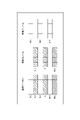
- the figure which shows the operation of the display device of the comparative example. The figure which shows typically the image data supplied to a display device.
- the figure which shows the operation of the display device of 1st Embodiment. The figure which illustrates the light emission amount of the comparative example and 1st Embodiment.
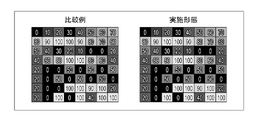
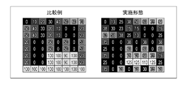
- the figure which compares the operation of the comparative example and 1st Embodiment. The figure which compares the operation of the comparative example and 1st Embodiment.
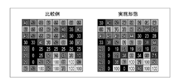
- the figure which compares the operation of the comparative example and 1st Embodiment The figure which shows the structure of the display device of 2nd Embodiment. The figure which shows the operation of the display device of 2nd Embodiment. The figure which shows the application example of the display device of embodiment. The figure which shows the application example of the display device of embodiment. The figure which shows the application example of the display device of embodiment. The figure which shows the application example of the display device of embodiment. The figure which shows the application example of the display device of embodiment. The figure which shows the application example of the display device of embodiment. The figure which shows the application example of the display device of embodiment. The figure which shows the application example of the display device of embodiment. The figure which shows the application example of the display device of embodiment. The figure which shows the application example of the display device of embodiment. The figure which shows the application example of the display device of embodiment. The figure which shows the application example of the display device of embodiment. The figure which shows the application example of the display device of embodiment. The figure which shows the application example of the display device of embodiment. The figure
- FIG. 1 shows the configuration of the display device DD1 of the comparative example.
- the display device DD1 has a function of displaying an image in which each frame is composed of at least two subframes.
- the display device DD1 may include a pixel array 10, a vertical scan control unit 11, a determination unit 12, a light emission period control unit 13, and a horizontal scan control unit 14.
- the display device DD1 can drive the pixel array 10 by a multi-line drive system that drives at least two rows of pixels at the same time.
- a multi-line drive system that drives at least two rows of pixels at the same time.
- the pixel array 10 has a plurality of pixels arranged so as to form a plurality of rows and a plurality of columns, and in FIG. 1, pixels 10 1 arranged in N-1 row, N row, and N + 1 row, respectively. 10 2 , 10 3 are typically shown. When a plurality of pixels are described without distinction, they are described as pixels 10 x . Such a notation is the same for other components.
- Each pixel 10 x may include transistors Tr1, Tr2, Tr3, a capacitance C, and a light emitting element EL (for example, an organic EL element).
- the gate of the transistor Tr1 is connected to a vertical scanning line VSL x (... VSL N-1 , VSL N , VSL N + 1 ) driven by the vertical scanning control unit 11.
- the vertical scan line VSL x is activated when writing a pixel signal to the capacitance C through the data DL x (DL 1 , DL 2 ...) Driven by the horizontal scan control unit 14.
- the transistor Tr2 supplies a current corresponding to the pixel signal written in the capacitance C to the light emitting element EL.
- the gate of the transistor Tr3 is connected to the light emission period signal line EP x (... EP N-1 , EP N , EP N + 1 ) driven by the light emission period control unit 13 to control the light emission period of the light emitting element EL.
- the image data ID of each frame supplied to the display device DD1 may include even-numbered subframe data which is even-numbered subframe data and odd-numbered subframe data which is odd-numbered subframe data.
- the transistors Tr1 of the pixels 10 1 , 10 2 of the N-1, N rows are driven so that the pixels 10 1 , 10 2 of the N-1, N rows are driven at the same time. Be controlled.
- the transistors Tr1 of the pixels 10 2 , 10 3 of the N, N + 1 rows are controlled so that the pixels 10 2 , 10 3 of the N, N + 1 rows are driven at the same time.
- the vertical scanning control unit 11 has a plurality of selection units 11 x (111 1 , 112, 11 3 ) .
- the plurality of selection units 11x may be arranged so that one selection unit 11x is assigned to one row.
- the image data ID of each frame is supplied to the determination unit 12.
- the determination unit 12 determines which subframe data of the two subframes constituting the frame is the current subframe data supplied, and the selection signal RAS indicating the result of the determination. RSB can be output.
- the current subframe data being supplied can be even subframe data or odd subframe data.
- the selection signal RSA or RSB may be a complementary or exclusive signal, and the selection signal RSA may be a signal obtained by inverting the selection signal RSA.
- the determination unit 12 may drive the selection signal RSA to the active level and the selection signal RSA to the inactive level when writing the pixel data of the even subframe data.
- the determination unit 12 may drive the selection signal RSA to the active level and the selection signal RSB to the inactive level when writing the pixel data of the odd-numbered subframe data.
- the determination unit 12 determines which subframe data of the at least two subframes constituting the frame is the current subframe data. Can be configured.
- Each selection unit 11 x of the vertical scan control unit 11 may be configured by a multiplexer that outputs a signal having the same logic level as the input signal designated by the selection signal among the first and second input signals.
- the selection unit 11 x to which the selection signal RSA is input outputs a signal having the same logic level as the first input signal when the selection signal RSA is the active level, and is the first when the selection signal RSA is the inactive level. 2
- a signal having the same logic level as the input signal can be output.
- the selection unit 11 x to which the selection signal RSB is input outputs a signal having the same logic level as the first input signal when the selection signal RSB is the active level, and is the first when the selection signal RSB is the inactive level.
- Each selection unit 11 x drives the vertical scan line VSL x of the corresponding row by its output.
- the selection unit 112 assigned to the N line outputs a signal having the same logic level as the line selection signal RN to the vertical scanning signal line VSL N when writing the pixel data of the even subframe data.
- the horizontal scanning control unit 14 outputs a pixel signal to the data line DL x of each column in order to write (that is, charge or discharge) the pixel signal to the capacitance C for controlling the emission brightness of each pixel 10 x .
- the capacity C of the pixels 10 1 , 10 2 of the N-1 row and the N row corresponds to the pixel data of the N row of the even subframe data.
- the pixel signal PN is written. That is, the pixel signal PN corresponding to the pixel data in the N row is written in the capacity C of the pixel 102 in the N row, and the adjacent pixel N is also written in the capacity C in the pixel 101 in the N- 1 row.
- the pixel signal PN corresponding to the pixel data of 102 of the pixels in the row is written.
- the pixel signal PN + 1 corresponding to the pixel data of the N + 1 row of the odd-numbered subframe data is written in the capacitance C of the pixels 102 and 103 in the N and N + 1 rows. That is, the pixel signal PN + 1 corresponding to the pixel data of the pixel 103 of N + 1, which is an adjacent pixel thereof, is written in the capacity C of the pixel 102 in the N row, and the capacity C of the pixel 102 in the N + 1 row is also written.
- the pixel signal PN + 1 corresponding to the pixel data of the pixel 103 of N + 1 is written.
- the light emission of the pixel 102 in the Nth row is perceived by humans as light emission corresponding to PN / 2 + PN + 1/2 in the two subframe periods.
- the image data ID is a still image (repetition of the same image) and the luminance levels of the pixels in rows N-1, N, and N + 1 are 20, 20, and 80.
- the light emission of the pixel 102 in the Nth row is perceived as an integrated average of 20, 20, and 80, that is, a brightness of 50, a deviation occurs from the original pixel data of 20, and the image quality deteriorates. sell.
- the display device DD2 of the first embodiment may have a function of displaying an image in which each frame is composed of at least two subframes.
- the display device DD2 may include a pixel array 10, a drive unit DRV for driving the pixel array 10, and a determination unit 12.
- the drive unit DRV may include a vertical scan control unit 11, a light emission period control unit 23, and a horizontal scan control unit 14.
- the display device DD2 can drive the pixel array 10 by a multi-line drive system that simultaneously drives at least two rows of pixels.
- a multi-line drive system that simultaneously drives at least two rows of pixels.
- FIG. 3 schematically shows an image data ID supplied to the display device DD2 (and the display device DD1).
- N-3 line, N-2 line, N-1 line, N line, N + 1 line, and N + 2 line of one frame of the image data ID are shown.
- the image data ID of one frame may be composed of two subframe data, specifically even subframe data and odd subframe data.
- the even subframe data is composed of pixel data of ... N-2 line, N line, N + 2 line ...
- the odd subframe data is ... N-3, N-1, N + 1 line.
- ... Can be composed of row pixel data.
- the determination unit 12 has at least two subframes (here, even subframes and odd subframes, in which the current subframe data supplied constitutes a frame) for each frame based on the image data ID or the signal accompanying the image data ID. It is possible to determine which subframe data of the frame). This determination can be made, for example, by utilizing the feature that the scanning start of the vertical synchronization signal is shifted by 0.5H when the image data ID is supplied as an interlaced signal. Further, it is also possible to specify whether to start transmission from even-numbered subframe data or odd-numbered subframe data at the start of transmission of the image data ID, and make a determination based on this.
- the determination unit 12 may generate selection signals RSA and RSB based on such determination.
- the determination unit 12 can drive the selection signal RSA to the active level and the selection signal RSA to the inactive level when writing the pixel data of the even subframe data. Further, the determination unit 12 may drive the selection signal RSA to the active level and the selection signal RSB to the inactive level when writing the pixel data of the odd-numbered subframe data. In the odd subframe, the selection signal RSA is driven to the active bell, and in the even subframe, the selection signal RSA is driven to the active level, so that the selection signals RSA and RSB are alternately driven to the active level.
- the vertical scan control unit 11 generates a row selection signal R x for controlling vertical scan (row selection) of the pixel array 10.
- the row selection signal R x may be configured by, for example, a shift register.
- the row selection signal R x can be driven to the active level over a predetermined period in the order of R 1 , R 2 ... RN-1 , RN, RN + 1 ...
- the vertical scan control unit 11 vertically scans so that the pixels 10 1 , 10 2 of the N-1 and N rows are driven at the same time. Can generate a signal.
- the vertical scanning control unit 11 can generate a vertical scanning signal so that the pixels 10 2 , 10 3 in rows N and N + 1 are driven at the same time.
- the selection circuit 11 1 of the N-1 line When writing the pixel data of the even subframe data, the selection circuit 11 1 of the N-1 line vertically scans the signal having the same logic level as the line selection signal RN of the N line according to the selection signal RSA. It can be output to the signal line VSL N-1 . Further, when writing the pixel data of the even subframe data, the selection unit 112 of the N line outputs a signal having the same logic level as the line selection signal RN of the N line according to the selection signal RSB to the vertical scanning signal line of the N line. Can be output to VSL N.
- the selection unit 112 of the N line When writing the pixel data of the odd-numbered subframe data, the selection unit 112 of the N line sets a signal having the same logic level as the line selection signal RN + 1 of the N + 1 line according to the selection signal RSB to the vertical scanning signal line VSL N of the N line. -Can be output. Further, when writing the pixel data of the odd-numbered subframe data, the selection circuit 113 of the N + 1 line transfers a signal having the same logic level as the line selection signal RN + 1 of the N + 1 line according to the selection signal RSA to the vertical scanning signal line of the N + 1 line. It can be output to VSL N + 1 .
- the drive unit DRV may be configured to drive at least two rows of pixels 10 x based on the pixel data of each row of each subframe data.
- the drive unit DVR emits light in the first condition the pixels of the row that does not match the row in the current subframe data supplied, and emits light in the second condition the pixels of the row that matches the row in the current subframe data.
- a plurality of pixels 10 x can be driven so as to be driven.
- the second condition may be a condition in which the amount of light emitted when the pixels are caused to emit light according to the same pixel value is larger than that of the first condition.
- the first condition is that the light emitting period for causing the pixels to emit light is the first light emitting period
- the second condition is the second light emitting period for which the light emitting period for causing the pixels to emit light is longer than the first light emitting period. ..
- the light emission period control unit 23 controls each transistor Tr3 of the plurality of pixels 10 x so that the pixel 10 x of the row that does not match the row in the current subframe data supplied emits light according to the first light emission period. sell. Further, the light emission period control unit 23 can control each transistor Tr3 of the plurality of pixels 10x so that the pixels of the row matching the row in the current subframe data supplied emits light according to the second light emission period. ..
- the light emission period control unit 23 may include a period signal generation unit 25.
- the control signal generation unit 25 may generate a first period control signal EPAx that defines a first light emission period T1 and a second period control signal EPBx that defines a second light emission period T2 that is longer than the first light emission period T1.
- the light emission period control unit 23 may include a plurality of selection units 23 x ( 231, 23 2 , 23 3 ). The plurality of selection units 23 x may be arranged so that one selection unit 23 x is assigned to one row.
- Each selection unit 23 x has a first period control signal EPBx that determines the first light emission period T1 and a second period control signal EPAx (a plurality of control signals that include a second light emission period T2 that is longer than the first light emission period T1). Of these, the period control signal corresponding to the current subframe data can be selected and output.
- the transistor Tr3 of the pixel 10 x in each row can be controlled by the output of the corresponding selection unit among the plurality of selection units 23x.
- the first light emission period T1 is a light emission period shorter than the light emission period in the optimized comparative example
- the second light emission period T2 is a light emission period longer than the light emission period in the comparative example.
- the average of the first light emission period T1 and the second light emission period T2 may coincide with the light emission period in the comparative example.
- the first light emission period T1 is 40% of the longest period and the second light emission period is T2. It can be 100% of the minimum period.
- the first light emission period in the comparative example is 90% of the longest design period, for example, the first light emission period T1 may be 80% of the longest period and the second light emission period T2 may be 100% of the minimum period. ..
- the first period control signal EPAx and the second period control signal EPBx may be generated so as to continuously emit light of the light emitting element EL of the pixel 10 x , or cause the light emitting element EL of the pixel 10 x to emit light intermittently. It may be generated as follows.
- FIG. 5 illustrates driving of pixels 10x in even-numbered subframes and odd-numbered subframes by the display device DD2 of the first embodiment.
- FIG. 2 illustrates driving of pixels 10x in even-numbered subframes and odd-numbered subframes by the display device DD1 of the comparative example.
- Tr1 / G, Tr2 / G, and Tr3 / G are signals supplied to the gates of the transistors Tr1, Tr2, and Tr3.
- the light emitting period of the light emitting element EL of the pixels 10 1 , 10 3 in the N-1, N + 1 row is controlled according to the first period control signal EPA x that defines the first light emitting period T1 having a relatively short light emitting period. Can be done. Further, in the even-numbered subframe, the light emitting period of the light emitting element EL of the pixel 102 in the Nth row can be controlled according to the second period control signal EPB x that defines the second light emitting period T2 having a relatively long light emitting period.
- the light emitting period of the light emitting element EL of the pixel 102 in the Nth row can be controlled according to the first period control signal EPA x that defines the first light emitting period T1 having a relatively short light emitting period. Further, in the odd-numbered subframe, the light emitting period of the light emitting element EL of the pixels 10 1 , 10 3 in the N-1, N + 1 row is set according to the second period control signal EPBx that defines the second light emitting period T2 having a relatively long light emitting period. Can be controlled.
- the horizontal scanning control unit 14 generates a pixel signal (voltage signal) to be written in the capacitance C of the pixel 10 x of each column of the selected row based on the image data ID, and outputs the pixel signal (voltage signal) to the data line DL x of each column. sell.
- the scanning of the pixel array 10 by the vertical scanning control unit 11 and the output of the pixel signal to the data line DL x by the horizontal scanning control unit 14 can be controlled in synchronization with each other. In the multi-line drive, the same pixel signal can be written to two vertically adjacent pixels 10 x in each column.
- Each pixel 10 x can control the light emission of the light emitting element EL based on the vertical scan signal from the vertical scan control unit 11, the period control signal from the light emission period control unit 23, and the pixel signal from the horizontal scan control unit 14.
- the brightness of the light emitted from the light emitting element EL can be defined by the pixel signal (voltage signal) written in the capacitance C. Further, the light emitting period of the light emitting element EL can be controlled by the period control signals EPAx and EPBx.
- a pixel signal for the N-row pixel 102 may be written via the data line DL x for the capacitance C of the N-1, N - row pixels 10 1 , 10 2 .
- the light emitting element EL of the pixel 101 in the N- 1 row can control the light emitting period over the first light emitting period T1 defined by the first control signal EPA N-1 .
- the light emitting element EL of the pixel 102 in the Nth row can control the light emitting period over the second light emitting period T2 defined by the second control signal EPBN . As illustrated in FIG.
- the light emission amount of the light emitting element EL of the pixel 101 in the N- 1 line is the N-1 line that emits light over the first light emission period T1 defined by the first control signal EPA N-1 . It is larger than the light emitting amount of the light emitting element EL of the pixel 10 1 .
- pixel signals for pixels 10 3 in N + 1 rows may be written via the data line DL x for the capacitance C of pixels 10 2 , 10 3 in N, N + 1 rows.
- the light emitting element EL of the pixel 102 in the Nth row can control the light emitting period over the first light emitting period T1 defined by the first control signal EPA N.
- the light emitting element EL of the pixel 103 in the N + 1 row can control the light emitting period over the second light emitting period T2 defined by the second control signal EPB N + 1 .
- the light emitting element EL of the pixel 103 in the N + 1 row can control the light emitting period over the second light emitting period T2 defined by the first control signal EPA N + 1 .
- the light emission amount of the light emitting element EL of the pixel 10 3 in the N + 1 row is the light emission of the pixel 10 2 in the N row that emits light over the first light emission period T1 defined by the first control signal EPA N. It is larger than the light emission amount of the element EL.
- the multi-line drive of the comparative example and the multi-line drive of the first embodiment are compared.
- the first light emission period T1 is set to 0.75 times the light emission period of the comparative example
- the second light emission period T2 is set to 1.25 times the light emission period of the comparative example.
- the column on the left shows a comparative example
- the column on the right shows an embodiment.
- FIG. 7A is an image data ID (original image), and there is no difference between the comparative example and the embodiment.
- FIG. 7B shows the display result of the even subframe
- FIG. 7C shows the display result of the odd subframe.
- FIG. 7D shows the integrated average image of FIGS. 7B and 7C, that is, the visual recognition result.
- FIG. 7E shows the absolute value of the difference between FIGS. 7A and 7D.
- the average value of the absolute difference values in FIG. 7E is 21.3 in the comparative example and 15.9 in the first embodiment, and the visual image quality of the first embodiment is improved as compared with the comparative example.
- the difference in the first embodiment when the first light emitting period T1 is set to 0.5 times the light emitting period of the comparative example and the second light emitting period T2 is set to 1.5 times the light emitting period of the comparative example, the difference in the first embodiment.
- the average value of the absolute values is 10.6, which is more effective.
- the difference in the ratio of the first light emission period T1 and the second light emission period T2 of the first embodiment to the light emission period of the comparative example is increased, the fluctuation amount of the light emission luminance in one frame period becomes large, and it is visually recognized as a flicker. There is a possibility. Therefore, control with an upper limit of about 1.5 times is preferable, but the control is not limited to this.
- the quality of the displayed image can be improved by using only the current subframe data supplied, so that the quality of the displayed image can be improved with a simple configuration as compared with the method using a frame memory or the like. Can be improved.
- a method of generating a signal for controlling the light emission period based on a triangular wave can be considered.
- the light emission period is controlled by using a method of controlling the threshold value at the time of pulse conversion as variable for each row and a method of controlling the slope of the triangular wave as variable for each row. It is possible to do.
- the light emitting element EL may be an organic EL element or another element. Further, the light emitting element EL may be replaced with a liquid crystal element. In this case, for example, a method of adjusting the brightness by controlling the lighting period of the backlight line by line based on the period control signal of the first embodiment can be considered. In addition, the same effect can be obtained by performing writing that clears the charge held in the pixel capacitance when the liquid crystal is driven according to the light emission period and making the light emission period variable for each line according to the period control signal. Can be done.
- the display device DD3 of the second embodiment will be described with reference to FIG. Items not mentioned as the configuration and operation of the display device DD3 of the second embodiment may follow the configuration and operation of the display device DD2 of the first embodiment.
- the display device DD3 may have a function of displaying an image in which each frame is composed of at least two subframes.
- the display device DD3 may include a pixel array 80, a drive unit DRV'that drives the pixel array 80, and a determination unit 12.
- the drive unit DRV' may include a vertical scan control unit 11 and a horizontal scan control unit 84.
- the display device DD3 can drive the pixel array 80 by a multi-line drive system that simultaneously drives at least two rows of pixels.
- a multi-line drive system that simultaneously drives at least two rows of pixels.
- the pixel array 80 has a plurality of pixels arranged so as to form a plurality of rows and a plurality of columns, and in FIG. 8, the pixels 80 1 arranged in the N-1 row, the N row, and the N + 1 row, respectively. , 802 , 803 are typically shown. When a plurality of pixels are described without distinction, they are described as pixels 80 x . Such a notation is the same for other components.
- Each pixel 80 x may include transistors Tr1, Tr2, a capacitance C, and a light emitting element EL (for example, an organic EL element).
- the pixel 80 x in the display device DD3 of the second embodiment may have a structure in which the transistor Tr3 is removed from the pixel 10 x in the display device DD2 of the first embodiment, but the pixel 80 x may also have the transistor Tr3. good.
- the display device DD3 may include a light emitting period control unit 13 in the display device DD1 of the comparative example.
- the gate (Tr1 / G) of the transistor Tr1 is connected to a vertical scanning line VSL x (... VSL N-1 , VSL N , VSL N + 1 ) driven by the vertical scanning control unit 11.
- the vertical scan line VSL x is activated when writing a pixel signal to the capacitance C through the data DLA x , DLB x (DLA 1 , DLB 1 , DLA 2 , DLB 2 , ...) Driven by the horizontal scan control unit 84. Will be done.
- the transistor Tr2 can supply the light emitting element EL with a current corresponding to the pixel signal written in the capacitance C.
- the drive unit DRV' can be configured to drive at least two rows of pixels 80x based on the pixel data of each row of each subframe data.
- the drive unit DVR' lights the pixels of the row that does not match the row in the supplied current subframe data under the first condition, and emits the pixels of the row that matches the row in the current subframe data under the second condition.
- a plurality of pixels 80x can be driven so as to emit light.
- the second condition may be a condition in which the emission intensity (luminance) is stronger than the first condition.
- the horizontal scanning control unit 84 which constitutes a part of the drive unit DRV', supplies a pixel signal to the pixels of the row that does not match the row in the first subframe data of at least two subframe data.
- Can include x .
- the horizontal scanning control unit 84 may include a second data line DLB x that supplies a pixel signal to the pixels of the row corresponding to the row in the second subframe data of at least two subframe data. More specifically, the horizontal scanning control unit 84 supplies a pixel signal to the pixels 80 1 and 803 of the N-1 row that do not match the N rows in the odd subframe data among the even subframe data and the odd subframe data.
- the first data line DLA x to be used may be included.
- the horizontal scanning control unit 84 includes a second data line DLB x that supplies a pixel signal to the pixel 802 of the N row matching the N row in the even subframe data among the even subframe data and the odd subframe data. sell.
- the pixels 80 x connected to the first data line DLA x and the pixels 80 x connected to the second data line DLB x may be arranged alternately.
- the transistor Tr1 of the pixels 80 1 and 802 of the N - 1 and N rows is driven so that the pixels 80 1 and 802 of the N-1 and N rows are driven at the same time. Can be controlled.
- the transistor Tr1 of the pixels 802 and 803 of the N and N + 1 rows can be controlled so that the pixels 802 and 803 of the N and N + 1 rows are driven at the same time.
- the vertical scanning control unit 11 has a plurality of selection units 11 x (111 1 , 112, 11 3 ) .
- the horizontal scanning control unit 84 When writing the pixel data of the even subframe data, the horizontal scanning control unit 84 supplies the first data line DLA x and the second data line DLB x , respectively, based on the pixel data of N rows of the image data ID. Generate a pixel signal. At this time, the horizontal scanning control unit 84 generates pixel signals to be supplied to the first data line DLA x and the second data line DLB x so as to satisfy the first condition and the second condition, respectively. Specifically, when writing pixel data of even subframe data, the horizontal scanning control unit 84 supplies the value of the pixel signal supplied to the second data line DLB x to the first data line DLA x . Can be greater than the value.
- the horizontal scanning control unit 84 supplies a pixel signal corresponding to d— ⁇ ( ⁇ is a positive numerical value) to the first data line DLAx.
- the second data line DLBx can be supplied with a pixel signal corresponding to d + ⁇ ( ⁇ is a positive numerical value).
- the value of ⁇ may be equal to or different from the value of ⁇ .
- the pixel signal supplied to the first data line DLA x is written to the capacitance C of the pixel 801 in the N- 1 row through the transistor Tr1 of the pixel 801 in the N-1 row.
- the pixel signal supplied to the second data line DLB x is written to the capacitance C of the pixel 802 of the N row through the transistor Tr 1 of the pixel 802 of the N row.
- the emission intensity of the pixel 802 of the N row driven according to the pixel data of the N row is larger than the emission intensity of the pixel 801 of the N- 1 row driven according to the pixel data of the N row.
- the horizontal scanning control unit 84 When writing the pixel data of the odd subframe data, the horizontal scanning control unit 84 supplies the first data line DLA x and the second data line DLB x , respectively, based on the pixel data of N + 1 rows of the image data ID. Generate a pixel signal. At this time, the horizontal scanning control unit 84 generates pixel signals to be supplied to the first data line DLAx and the second data line DLBx so as to satisfy the first condition and the second condition, respectively. Specifically, when writing the pixel data of the odd subframe data, the horizontal scanning control unit 84 supplies the value of the pixel signal supplied to the first data line DLA x to the second data line DLB x . Can be greater than the value.
- the horizontal scanning control unit 84 supplies a pixel signal corresponding to d + ⁇ ( ⁇ is a positive numerical value) to the first data line DLA x .
- a pixel signal corresponding to d— ⁇ ( ⁇ is a positive numerical value) can be supplied to the second data line DLB x .
- the value of ⁇ may be equal to or different from the value of ⁇ .
- the pixel signal supplied to the first data line DLA x is written to the capacitance C of the pixel 803 of the N + 1 row through the transistor Tr1 of the pixel 803 of the N + 1 row.
- the pixel signal supplied to the second data line DLB x is written to the capacitance C of the pixel 802 of the N row through the transistor Tr 1 of the pixel 802 of the N row.
- the emission intensity of the pixel 803 of the N + 1 row driven according to the pixel data of the N + 1 row becomes larger than the emission intensity of the pixel 802 of the N row driven according to the pixel data of the N + 1 row.
- the process of determining the pixel signal to be supplied to the first data line DLA x and the second data line DLB x based on the pixel data of each row (and each column) of the image data ID is a process of determining the pixel signal by correcting the data. It can also be understood as a correction process for obtaining. This correction process may be a process of performing linear or non-linear correction to the pixel data of each row of the image data ID.
- the pixel in the Nth row of the image data ID (original image) is a pixel in the low brightness region
- a correction is made so as to increase the pixel value of the pixel in an even field to generate a pixel signal.
- Display image can be generated. Therefore, for pixels in the low-luminance region, it is preferable to generate a pixel signal so as to suppress the brightness to equal to or less than the brightness in the original image.
- a value without the above correction may be output to the data line. Further, the above correction may be made so that the luminance step is not formed, that is, the luminance gradually changes.
- the pixels of the row that does not match the row in the supplied current subframe data are made to emit light under the first condition, and the pixels of the row that matches the row in the current subframe data are emitted. Is emitted under the second condition, which has a larger amount of light emission than the first condition.
- an arbitrary correction process can be adopted, and further improvement in the quality of the displayed image can be expected.
- the display device of the first and second embodiments is a display device that drives a plurality of rows including the first row with data based on the same data by using image data in which one frame is composed of at least two subframes.
- the 1 frame includes a first subframe that drives the first row and other rows of the plurality of rows with data based on the drive data of the first row, and the first row and the said row. It has a second subframe in which another row among the plurality of rows is driven by data based on the driving data of the other row, and at least one pixel included in the first row is the first sub. It can also be said that the display device has a light emitting amount in the frame larger than the light emitting amount in the second subframe.
- FIG. 10 is a schematic diagram showing an application example of the above-mentioned first and second display devices DD2 and DD3.
- the display device 1000 includes a display panel 1005, a frame 1006, a circuit board 1007, and a battery 1008, which are composed of a touch panel 1003 and a display device typified by the display device DD2 or DD3 between the upper cover 1001 and the lower cover 1009. , May have.
- Flexible print circuits FPC1002 and 1004 are connected to the touch panel 1003 and the display panel 1005.
- a transistor is printed on the circuit board 1007.
- the battery 1008 may not be provided if the display device 1000 is not a portable device, or may be provided at a different position even if it is a portable device.
- the display device may be used for a display unit of an image pickup device having an optical unit having a plurality of lenses and an image pickup element that receives light that has passed through the optical unit.
- the image pickup apparatus may have a display unit that displays information acquired by a plurality of image pickup elements included in the image pickup unit. Further, the information may be acquired by using the information acquired by the image sensor, and the display unit may display information other than the information.
- the image pickup device may be a digital camera or a digital video camera.
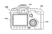
- FIG. 11A is a schematic diagram showing an example of an image pickup apparatus according to an embodiment.
- the image pickup apparatus 1100 may include a view finder 1101, a rear display 1102, an operation unit 1103, and a housing 1104.
- the viewfinder 1101 may include a display unit composed of a display device typified by the display device DD2 or DD3. In that case, the display device may display not only the image to be captured but also environmental information, imaging instructions, and the like.
- the environmental information may include the intensity of the outside light, the direction of the outside light, the moving speed of the subject, the possibility that the subject is shielded by a shield, and the like.
- the light emitting device may be composed of an organic light emitting device having a high response speed.
- the image pickup apparatus 1100 has an optical unit (not shown).
- the optical unit has a plurality of lenses and forms an image on an image pickup element housed in the housing 1104.
- the focal point of a plurality of lenses can be adjusted by adjusting their relative positions. This operation can also be performed automatically.
- the display device of the embodiment may have a color filter having red, green, and blue.
- the color filter may be arranged in a delta arrangement of the red, green, and blue.
- the display device of the embodiment may be used for the display unit of the mobile terminal. In that case, it may have both a display function and an operation function. Examples of the mobile terminal include a mobile phone such as a smartphone, a tablet, a head-mounted display, and the like.
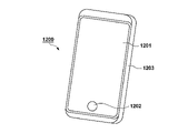
- FIG. 11B is a schematic diagram showing an example of an electronic device according to an embodiment.
- the electronic device 1200 has a display unit 1201 composed of a display device typified by the display device DD2 or DD3, an operation unit 1202, and a housing 1203.
- the housing 1203 may include a circuit, a printed circuit board having the circuit, a battery, and a communication unit.
- the operation unit 1202 may be a button or a touch panel type reaction unit.
- the operation unit may be a biometric recognition unit that recognizes a fingerprint and unlocks the lock.
- An electronic device having a communication unit can also be called a communication device.
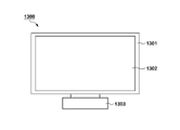
- FIG. 12A and 12B are schematic views showing an example of a display device according to an embodiment.
- FIG. 12A is a display device such as a television monitor or a PC monitor.
- the display device 1300 has a frame 1301 and a display unit 1302.
- the display unit 1302 may be composed of a display device typified by the display device DD2 or DD3.
- the display device 1300 has a frame 1301 and a base 1303 that supports the display unit 1302.
- the base 1303 is not limited to the form shown in FIG. 12A.
- the lower side of the frame 1301 may also serve as a base. Further, the frame 1301 and the display unit 1302 may be bent.
- the radius of curvature may be 5000 mm or more and 6000 mm or less.
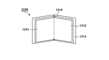
- FIG. 12B is a schematic diagram showing another example of the display device according to the embodiment.
- the display device 1310 of FIG. 12B is configured to be foldable and is a so-called foldable display device.
- the display device 1310 has a first display unit 1311, a second display unit 1312, a housing 1313, and a bending point 1314.
- a display device represented by the display device DD2 or DD3 can be applied to the first display unit 1311 and the second display unit 1312.
- the first display unit 1311 and the second display unit 1312 may be a single display device having no joint.
- the first display unit 1311 and the second display unit 1312 can be separated by a bending point.
- the first display unit 1311 and the second display unit 1312 may display different images, or the first and second display units may display one image.
- FIG. 13A is a schematic diagram showing an example of a lighting device according to an embodiment.
- the lighting device 1400 may include a housing 1401, a light source 1402, a circuit board 1403, an optical film 1404, and a light diffusing unit 1405.
- a light emitting device 100 may be applied to the light source 1402.
- the optical filter may be a filter that improves the color rendering property of the light source.
- the light diffusing unit can effectively diffuse the light of the light source such as lighting up and deliver the light to a wide range.
- the optical filter and the light diffusing unit may be provided on the light emitting side of the illumination. If necessary, a cover may be provided on the outermost side.
- the lighting device is, for example, a device that illuminates a room.
- the illuminating device may emit white, neutral white, or any other color from blue to red. It may have a dimming circuit for dimming them.
- the lighting device may have the organic light emitting element of the present invention and a power supply circuit connected to the organic light emitting element.
- the power supply circuit is a circuit that converts an AC voltage into a DC voltage.
- white has a color temperature of 4200 K
- neutral white has a color temperature of 5000 K.
- the illuminator may have a color filter.
- the lighting device according to the present embodiment may have a heat radiating unit.
- the heat radiating unit releases the heat inside the device to the outside of the device, and examples thereof include a metal having a high specific heat and liquid silicon.
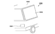
- FIG. 13B is a schematic diagram of an automobile which is an example of a moving body according to an embodiment.
- the car has a tail lamp, which is an example of a lamp.
- the automobile 1500 may have a tail lamp 1501 and may be in a form of turning on the tail lamp when a brake operation or the like is performed.
- a display panel composed of a display device represented by the display device DD2 or DD3 can be applied to the tail lamp 1501.
- the tail lamp may have a protective member that protects the light emitting element.
- the protective member has a certain degree of high strength, and any material may be used as long as it is transparent, but it is preferably made of polycarbonate or the like.
- a flange carboxylic acid derivative, an acrylonitrile derivative, or the like may be mixed with the polycarbonate.
- the automobile 1500 may have a vehicle body 1503 and a window 1502 attached to the vehicle body 1503.
- the window may be a transparent display as long as it is not a window for checking the front and back of the car.
- a light emitting device 100 may be applied to the transparent display.
- the constituent material such as the electrode of the organic light emitting element is composed of a transparent member.
- the moving body according to the present embodiment may be a ship, an aircraft, a drone, or the like.
- the moving body may have an airframe and a lamp provided on the airframe.
- the lamp may emit light to indicate the position of the aircraft.
- a display panel composed of a display device represented by the display device DD2 or DD3 may be applied to the lamp.
- the display device can be applied to a system that can be worn as a wearable device such as smart glasses, HMDs, and smart contacts.
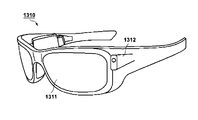
- FIG. 14A illustrates eyeglasses 1600 (smart glasses) according to one application example.
- An image pickup device 1602 such as a CMOS sensor or SPAD is provided on the surface side of the lens 1601 of the spectacles 1600. Further, on the back surface side of the lens 1601, a display device to which the light emitting device 100 is applied is provided.
- the glasses 1600 further include a control device 1603.
- the control device 1603 functions as a power source for supplying electric power to the image pickup device 1602 and the display device according to each embodiment. Further, the control device 1603 controls the operation of the image pickup device 1602 and the display device.
- the lens 1601 is formed with an optical system for condensing light on the image pickup apparatus 1602.
- FIG. 14B illustrates eyeglasses 1610 (smart glasses) according to one application example.
- the spectacles 1610 has a control device 1612, and the control device 1612 is equipped with an image pickup device corresponding to the image pickup device 1602 and a display device.
- the lens 1611 is formed with an image pickup device in the control device 1612 and an optical system for projecting light emitted from the display device, and an image is projected on the lens 1611.
- the control device 1612 functions as a power source for supplying electric power to the image pickup device and the display device, and controls the operation of the image pickup device and the display device.
- the control device may have a line-of-sight detection unit that detects the line of sight of the wearer. Infrared rays may be used to detect the line of sight.
- the infrared light emitting unit emits infrared light to the eyeball of the user who is gazing at the displayed image.
- An image captured by the eyeball is obtained by detecting the reflected light of the emitted infrared light from the eyeball by the image pickup unit having a light receiving element.
- the user's line of sight to the displayed image is detected from the captured image of the eyeball obtained by imaging infrared light. Any known method can be applied to the line-of-sight detection using the captured image of the eyeball. As an example, a line-of-sight detection method based on a Purkinje image by reflection of irradiation light on the cornea can be used.
- the line-of-sight detection process based on the pupillary corneal reflex method is performed.
- the user's line of sight is detected by calculating the line-of-sight vector representing the direction (rotation angle) of the eyeball based on the image of the pupil and the Purkinje image included in the captured image of the eyeball using the pupillary corneal reflex method.
- the display device has an image pickup device having a light receiving element, and may control the display image of the display device based on the user's line-of-sight information from the image pickup device.
- the display device determines a first visual field region to be watched by the user and a second visual field region other than the first visual field region based on the line-of-sight information.
- the first field of view area and the second field of view area may be determined by the control device of the display device, or may receive those determined by the external control device.
- the display resolution of the first field of view area may be controlled to be higher than the display resolution of the second field of view area. That is, the resolution of the second field of view may be lower than that of the first field of view.
- the display area has a first display area and a second display area different from the first display area, and the priority is given from the first display area and the second display area based on the line-of-sight information. Is determined in the high area.
- the first field of view area and the second field of view area may be determined by the control device of the display device, or may receive those determined by the external control device.
- the resolution of the high-priority area may be controlled higher than the resolution of the non-high-priority area. That is, the resolution of the region having a relatively low priority may be lowered.
- AI may be used to determine the first field of view area or the area with high priority.
- AI is a model configured to estimate the angle of the line of sight and the distance to the object ahead of the line of sight from the image of the eyeball, using the image of the eyeball and the direction in which the eyeball of the image was actually viewed as teacher data. It may be there.
- the AI program may be possessed by the display device, the image pickup device, or the external device. If the external device has it, it is transmitted to the display device via communication.
- the display When the display is controlled based on the visual detection, it can be preferably applied to smart glasses having an image pickup device that images the outside. Smart glasses can display captured external information in real time.
- DD2 Display device
- 10 x , 80 x Pixel
Landscapes
- Engineering & Computer Science (AREA)
- General Physics & Mathematics (AREA)
- Theoretical Computer Science (AREA)
- Physics & Mathematics (AREA)
- Computer Hardware Design (AREA)
- Inorganic Chemistry (AREA)
- Chemical & Material Sciences (AREA)
- Sustainable Development (AREA)
- Life Sciences & Earth Sciences (AREA)
- Control Of Indicators Other Than Cathode Ray Tubes (AREA)
- Control Of El Displays (AREA)
- Multimedia (AREA)
- Signal Processing (AREA)
- Electroluminescent Light Sources (AREA)
- Transforming Electric Information Into Light Information (AREA)
Abstract
Description
Claims (14)
- 少なくとも2つのサブフレームで各フレームが構成される画像を表示するように構成された表示装置であって、
供給される各サブフレームデータの各行の画素データに基づいて少なくとも2行の画素を駆動するように、画素アレイの複数の画素を駆動する駆動部を備え、
前記駆動部は、供給されている現在のサブフレームデータにおける行と一致しない行の画素を第1条件で発光させ、該現在のサブフレームデータにおける行と一致する行の画素を第2条件で発光させるように、前記複数の画素を駆動し、
前記第2条件は、同一画素値に従って画素を発光させた場合における発光量が前記第1条件よりも大きい条件である、
ことを特徴とする表示装置。 - 前記第1条件は、画素を発光させる発光期間が第1発光期間であり、前記第2条件は、画素を発光させる発光期間が前記第1発光期間よりも長い第2発光期間である、
ことを特徴とする請求項1に記載の表示装置。 - 前記複数の画素の各々は、発光期間を制御するトランジスタを含み、
前記駆動部は、供給されている現在のサブフレームデータにおける行と一致しない行の画素を前記第1発光期間に従って発光させ、該現在のサブフレームにおける行と一致する行の画素を前記第2発光期間に従って発光させるように、前記複数の画素の各々の前記トランジスタを制御する、
ことを特徴とする請求項2に記載の表示装置。 - 前記駆動部は、1つの選択部が1つの行に割り当てられるように配置された複数の選択部を含み、各選択部は、第1発光期間を定める第1制御信号と、前記第1発光期間より長い第2発光期間を定める第2制御信号を含む複数の制御信号のうち供給されている現在のサブフレームデータに対応する制御信号を選択して出力し、
各行の画素の前記トランジスタは、前記複数の選択部のうち対応する選択部の出力によって制御される、
ことを特徴とする請求項3に記載の表示装置。 - 前記第2条件は、発光強度が前記第1条件より強い条件である、
ことを特徴とする請求項1に記載の表示装置。 - 前記複数の画素の各々は、メモリを含み、前記メモリに書き込まれた信号に応じて発光するように構成され、
前記駆動部は、前記第1条件および前記第2条件を満たすように、供給されている現在のサブフレームデータに基づいて前記複数の画素の各々の前記メモリに書き込む画素信号を制御する、
ことを特徴とする請求項5に記載の表示装置。 - 前記駆動部は、供給されているサブフレームデータのうちの第1サブフレームデータにおける行と一致する行の画素に画素信号を供給する第1データ線と、該供給されているサブフレームデータのうちの第2サブフレームデータにおける行と一致する行の画素に画素信号を供給する第2データ線とを含み、
前記駆動部は、前記第1条件および前記第2条件を満たすように、供給されている現在のサブフレームデータに基づいて、前記第1データ線および前記第2データ線に供給する画素信号を制御する、
ことを特徴とする請求項6に記載の表示装置。 - 前記少なくとも2つのサブフレームは、偶数サブフレームおよび奇数サブフレームを含む、
ことを特徴とする請求項1乃至7のいずれか1項に記載の表示装置。 - 供給されている現在のサブフレームデータが前記少なくとも2つのサブフレームのいずれのサブフレームデータであるかを判定する判定部を更に備える、
ことを特徴とする請求項1乃至8のいずれか1項に記載の表示装置。 - 被写体を撮像する撮像部と、
前記撮像部からのデータに基づいて画像を表示するように構成された請求項1乃至9のいずれか1項に記載の表示装置と、
を備えることを特徴とする電子装置。 - 被写体を撮像する撮像部と、
前記撮像部からのデータに基づいて画像を表示するように構成された請求項1乃至9のいずれか1項に記載の表示装置と、
を備えることを特徴とする移動体。 - 少なくとも2つのサブフレームで1フレームが構成された画像データを用いて、第一行を含む複数の行を同じデータに基づくデータで駆動する表示装置であって、
前記1フレームは、前記第一行及び前記複数の行のうちの他の行を前記第一行の駆動データに基づくデータで駆動する第一サブフレームと、前記第一行及び前記複数の行のうちの他の行を前記他の行の駆動データに基づくデータで駆動する第二サブフレームと、を有し、
前記第一行に含まれる少なくとも1つの画素は、前記第一サブフレームにおける発光量が、前記第二サブフレームにおける発光量よりも大きいこと、
を特徴とする表示装置。 - 前記少なくとも2つのサブフレームは、偶数サブフレームおよび奇数サブフレームを含む、
ことを特徴とする請求項12に記載の表示装置。 - 前記駆動データにより、前記第一サブフレームまたは前記第二サブフレームであることをと判別する判別手段をさらに有する請求項12または13に記載の表示装置。
Priority Applications (3)
| Application Number | Priority Date | Filing Date | Title |
|---|---|---|---|
| CN202180069768.2A CN116368552B (zh) | 2020-10-12 | 2021-10-06 | 显示装置、电子设备和移动体 |
| KR1020237013403A KR102669390B1 (ko) | 2020-10-12 | 2021-10-06 | 표시장치, 전자장치 및 이동체 |
| US18/184,987 US11972718B2 (en) | 2020-10-12 | 2023-03-16 | Display device, electronic apparatus, and moving body |
Applications Claiming Priority (2)
| Application Number | Priority Date | Filing Date | Title |
|---|---|---|---|
| JP2020-172134 | 2020-10-12 | ||
| JP2020172134A JP7492432B2 (ja) | 2020-10-12 | 2020-10-12 | 表示装置、電子装置および移動体 |
Related Child Applications (1)
| Application Number | Title | Priority Date | Filing Date |
|---|---|---|---|
| US18/184,987 Continuation US11972718B2 (en) | 2020-10-12 | 2023-03-16 | Display device, electronic apparatus, and moving body |
Publications (1)
| Publication Number | Publication Date |
|---|---|
| WO2022080201A1 true WO2022080201A1 (ja) | 2022-04-21 |
Family
ID=81208045
Family Applications (1)
| Application Number | Title | Priority Date | Filing Date |
|---|---|---|---|
| PCT/JP2021/036922 Ceased WO2022080201A1 (ja) | 2020-10-12 | 2021-10-06 | 表示装置、電子装置および移動体 |
Country Status (5)
| Country | Link |
|---|---|
| US (1) | US11972718B2 (ja) |
| JP (1) | JP7492432B2 (ja) |
| KR (1) | KR102669390B1 (ja) |
| CN (1) | CN116368552B (ja) |
| WO (1) | WO2022080201A1 (ja) |
Families Citing this family (1)
| Publication number | Priority date | Publication date | Assignee | Title |
|---|---|---|---|---|
| KR102809085B1 (ko) * | 2021-04-13 | 2025-05-20 | 삼성디스플레이 주식회사 | 표시 장치 및 이를 이용한 표시 패널의 구동 방법 |
Citations (4)
| Publication number | Priority date | Publication date | Assignee | Title |
|---|---|---|---|---|
| JP2003532145A (ja) * | 2000-04-19 | 2003-10-28 | コーニンクレッカ フィリップス エレクトロニクス エヌ ヴィ | イメージ鮮鋭度を改良したマトリクスディスプレイデバイス |
| JP2010271365A (ja) * | 2009-05-19 | 2010-12-02 | Sony Corp | 表示制御装置、表示制御方法 |
| WO2015087598A1 (ja) * | 2013-12-09 | 2015-06-18 | シャープ株式会社 | 画像表示装置およびその駆動方法 |
| JP2016110115A (ja) * | 2014-12-01 | 2016-06-20 | 三星ディスプレイ株式會社Samsung Display Co.,Ltd. | 表示装置およびその駆動方法 |
Family Cites Families (18)
| Publication number | Priority date | Publication date | Assignee | Title |
|---|---|---|---|---|
| JP3391331B2 (ja) | 1992-03-05 | 2003-03-31 | セイコーエプソン株式会社 | 液晶装置の駆動方法、液晶表示装置及び駆動回路 |
| US6243055B1 (en) * | 1994-10-25 | 2001-06-05 | James L. Fergason | Optical display system and method with optical shifting of pixel position including conversion of pixel layout to form delta to stripe pattern by time base multiplexing |
| US5748164A (en) * | 1994-12-22 | 1998-05-05 | Displaytech, Inc. | Active matrix liquid crystal image generator |
| TW441136B (en) * | 1997-01-28 | 2001-06-16 | Casio Computer Co Ltd | An electroluminescent display device and a driving method thereof |
| US6952194B1 (en) * | 1999-03-31 | 2005-10-04 | Semiconductor Energy Laboratory Co., Ltd. | Liquid crystal display device |
| US7030848B2 (en) * | 2001-03-30 | 2006-04-18 | Matsushita Electric Industrial Co., Ltd. | Liquid crystal display |
| US7812812B2 (en) | 2003-03-25 | 2010-10-12 | Canon Kabushiki Kaisha | Driving method of display apparatus |
| US7605899B2 (en) | 2003-12-05 | 2009-10-20 | Canon Kabushiki Kaisha | Electrophoretic dispersion liquid and electrophoretic display device |
| JP2006039039A (ja) * | 2004-07-23 | 2006-02-09 | Tohoku Pioneer Corp | 自発光表示パネルの駆動装置、駆動方法及びその駆動装置を備えた電子機器 |
| US7453478B2 (en) * | 2004-07-29 | 2008-11-18 | Hewlett-Packard Development Company, L.P. | Address generation in a light modulator |
| US8847861B2 (en) * | 2005-05-20 | 2014-09-30 | Semiconductor Energy Laboratory Co., Ltd. | Active matrix display device, method for driving the same, and electronic device |
| US8339423B2 (en) * | 2005-08-29 | 2012-12-25 | Sharp Kabushiki Kaisha | Display apparatus, display method, display monitor, and television receiver |
| JP5361139B2 (ja) | 2007-03-09 | 2013-12-04 | キヤノン株式会社 | 表示装置 |
| JP6044063B2 (ja) * | 2011-11-15 | 2016-12-14 | 日亜化学工業株式会社 | 表示装置の点灯制御方法及び表示ユニット |
| JP5939076B2 (ja) * | 2012-07-31 | 2016-06-22 | ソニー株式会社 | 表示装置、駆動回路、駆動方法、および電子機器 |
| JP6484799B2 (ja) * | 2014-02-04 | 2019-03-20 | パナソニックIpマネジメント株式会社 | 投写型画像表示装置および調整方法 |
| KR102543350B1 (ko) * | 2018-08-16 | 2023-06-15 | 삼성전자주식회사 | 이미지 센서 |
| CN109461407B (zh) * | 2018-12-26 | 2020-10-16 | 上海天马微电子有限公司 | 一种有机发光显示面板及有机发光显示装置 |
-
2020
- 2020-10-12 JP JP2020172134A patent/JP7492432B2/ja active Active
-
2021
- 2021-10-06 KR KR1020237013403A patent/KR102669390B1/ko active Active
- 2021-10-06 CN CN202180069768.2A patent/CN116368552B/zh active Active
- 2021-10-06 WO PCT/JP2021/036922 patent/WO2022080201A1/ja not_active Ceased
-
2023
- 2023-03-16 US US18/184,987 patent/US11972718B2/en active Active
Patent Citations (4)
| Publication number | Priority date | Publication date | Assignee | Title |
|---|---|---|---|---|
| JP2003532145A (ja) * | 2000-04-19 | 2003-10-28 | コーニンクレッカ フィリップス エレクトロニクス エヌ ヴィ | イメージ鮮鋭度を改良したマトリクスディスプレイデバイス |
| JP2010271365A (ja) * | 2009-05-19 | 2010-12-02 | Sony Corp | 表示制御装置、表示制御方法 |
| WO2015087598A1 (ja) * | 2013-12-09 | 2015-06-18 | シャープ株式会社 | 画像表示装置およびその駆動方法 |
| JP2016110115A (ja) * | 2014-12-01 | 2016-06-20 | 三星ディスプレイ株式會社Samsung Display Co.,Ltd. | 表示装置およびその駆動方法 |
Also Published As
| Publication number | Publication date |
|---|---|
| CN116368552B (zh) | 2025-07-15 |
| US20230298506A1 (en) | 2023-09-21 |
| KR102669390B1 (ko) | 2024-05-28 |
| KR20230070288A (ko) | 2023-05-22 |
| CN116368552A (zh) | 2023-06-30 |
| JP2022063740A (ja) | 2022-04-22 |
| JP7492432B2 (ja) | 2024-05-29 |
| US11972718B2 (en) | 2024-04-30 |
Similar Documents
| Publication | Publication Date | Title |
|---|---|---|
| US12277909B2 (en) | Display device, photoelectric conversion device, electronic device, moving body, and wearable device | |
| US12075541B2 (en) | Light emitting device, control method thereof, photoelectric conversion device, electronic apparatus, illumination device, and moving body | |
| KR20000062993A (ko) | 액정 표시 장치 | |
| US12027123B2 (en) | Light emitting device having a pixel, a driving transistor, a light emission control transistor, a write transistor, and a capacitive element | |
| US11972718B2 (en) | Display device, electronic apparatus, and moving body | |
| US20230090509A1 (en) | Display apparatus, photoelectric conversion apparatus, electronic equipment, and mobile body | |
| KR20240158967A (ko) | 표시 장치 및 전자 기기 | |
| JP7832213B2 (ja) | 表示装置、電子機器、及び表示制御方法 | |
| WO2024084876A1 (ja) | 表示装置および電子機器 | |
| US12614517B2 (en) | Light emitting device, photoelectric conversion device, and electronic apparatus | |
| WO2023243474A1 (ja) | 表示装置 | |
| JP2024127499A (ja) | 発光素子、光電変換装置、電子機器、照明装置、移動体 | |
| US20260120631A1 (en) | Display device, display apparatus, photoelectric conversion apparatus, electronic apparatus, moving body, and wearable device | |
| US20250292735A1 (en) | Display device whose duty ratio in sub-frame period is controlled | |
| US20250265958A1 (en) | Light emitting device, image forming device, display device, image capturing device, electronic apparatus, illumination device, moving body, and wearable device | |
| JP7807901B2 (ja) | 表示装置、光電変換装置及び電子機器 | |
| JP2025077983A (ja) | 発光装置、光電変換装置及び電子機器 | |
| WO2024204135A1 (ja) | 表示装置、表示装置の駆動方法および電子機器 | |
| WO2024203011A1 (ja) | 表示装置及び電子機器 | |
| WO2025013397A1 (ja) | 表示装置 | |
| WO2025047426A1 (ja) | 表示装置及び表示方法 | |
| WO2026079245A1 (ja) | 表示装置及び表示システム | |
| WO2025239226A1 (ja) | 表示装置及び電子機器 | |
| CN118871967A (zh) | 显示装置 | |
| WO2024048268A1 (ja) | 表示装置、電子機器及び表示装置の駆動方法 |
Legal Events
| Date | Code | Title | Description |
|---|---|---|---|
| 121 | Ep: the epo has been informed by wipo that ep was designated in this application |
Ref document number: 21879941 Country of ref document: EP Kind code of ref document: A1 |
|
| ENP | Entry into the national phase |
Ref document number: 20237013403 Country of ref document: KR Kind code of ref document: A |
|
| NENP | Non-entry into the national phase |
Ref country code: DE |
|
| 122 | Ep: pct application non-entry in european phase |
Ref document number: 21879941 Country of ref document: EP Kind code of ref document: A1 |
|
| WWG | Wipo information: grant in national office |
Ref document number: 202180069768.2 Country of ref document: CN |