WO2022074728A1 - 訓練データ生成プログラム、訓練データ生成方法及び訓練データ生成装置 - Google Patents
訓練データ生成プログラム、訓練データ生成方法及び訓練データ生成装置 Download PDFInfo
- Publication number
- WO2022074728A1 WO2022074728A1 PCT/JP2020/037829 JP2020037829W WO2022074728A1 WO 2022074728 A1 WO2022074728 A1 WO 2022074728A1 JP 2020037829 W JP2020037829 W JP 2020037829W WO 2022074728 A1 WO2022074728 A1 WO 2022074728A1
- Authority
- WO
- WIPO (PCT)
- Prior art keywords
- training data
- circuit
- circuit information
- data generation
- generated
- Prior art date
- Legal status (The legal status is an assumption and is not a legal conclusion. Google has not performed a legal analysis and makes no representation as to the accuracy of the status listed.)
- Ceased
Links
Images


Classifications
-
- G—PHYSICS
- G06—COMPUTING OR CALCULATING; COUNTING
- G06F—ELECTRIC DIGITAL DATA PROCESSING
- G06F30/00—Computer-aided design [CAD]
- G06F30/20—Design optimisation, verification or simulation
- G06F30/27—Design optimisation, verification or simulation using machine learning, e.g. artificial intelligence, neural networks, support vector machines [SVM] or training a model
-
- G—PHYSICS
- G06—COMPUTING OR CALCULATING; COUNTING
- G06F—ELECTRIC DIGITAL DATA PROCESSING
- G06F30/00—Computer-aided design [CAD]
- G06F30/30—Circuit design
- G06F30/39—Circuit design at the physical level
- G06F30/398—Design verification or optimisation, e.g. using design rule check [DRC], layout versus schematics [LVS] or finite element methods [FEM]
-
- G—PHYSICS
- G06—COMPUTING OR CALCULATING; COUNTING
- G06N—COMPUTING ARRANGEMENTS BASED ON SPECIFIC COMPUTATIONAL MODELS
- G06N20/00—Machine learning
Definitions
- the present invention relates to a training data generation technique.
- EMI Electromagnetic Interference
- EMI refers to the electromagnetic wave radiation state radiated from an electronic circuit.
- EMI is also referred to as a distant field from the aspect of the electromagnetic wave radiation situation, which refers to the distant electromagnetic field situation.
- the EMI intensity in the circuit to be predicted is predicted using a trained machine learning model generated from the training data in which the circuit information and the simulation result of the electromagnetic wave analysis for the circuit information are associated with each other.
- the training data generation program calculates the characteristic impedance of the circuit included in each of the first plurality of circuit information, classifies the plurality of circuit information based on the calculated characteristic impedance, and classifies the plurality of circuit information.
- One or more circuit information is selected from the second plurality of circuit information classified into the first group by the processing of the above classification, and training for machine learning is performed based on the selected one or more circuit information. Generate data, let the computer perform the process.
- FIG. 1 is a block diagram showing an example of a functional configuration of the server device according to the first embodiment.
- FIG. 2 is a diagram showing an example of a simple circuit and a complicated circuit.
- FIG. 3 is a diagram showing an example of a machine learning method of an EMI prediction model.
- FIG. 4 is a diagram showing an example of EMI prediction of a complex circuit.
- FIG. 5 is a diagram showing an example of EMI prediction of a circuit with elements.
- FIG. 6 is a diagram showing an example of variations in substrate characteristics.
- FIG. 7 is a diagram showing another example of variations in substrate characteristics.
- FIG. 8 is a diagram showing one aspect of the relationship between the characteristic impedance and the EMI.
- FIG. 9 is a diagram showing an example of filtering.
- FIG. 9 is a diagram showing an example of filtering.
- FIG. 10 is a diagram showing an example of a circuit enumeration method.
- FIG. 11 is a diagram showing an example of a method of setting a dividing line of a line.
- FIG. 12 is a flowchart showing the procedure of the training data generation process according to the first embodiment.
- FIG. 13 is a diagram showing an application example of filtering.
- FIG. 14 is a diagram showing an example of hardware configuration of a computer.
- FIG. 1 is a block diagram showing an example of the functional configuration of the server device 10 according to the first embodiment.
- the server device 10 shown in FIG. 1 is an example of a computer that provides a training data generation function for generating training data used for training a machine learning model that predicts EMI intensity in an electronic circuit.
- a machine learning model for predicting EMI intensity in an electronic circuit may be referred to as an “EMI prediction model”.
- Such a training data generation function can be packaged as a function of a machine learning service that executes machine learning of an EMI prediction model using the above training data.
- the above-mentioned training data generation function or the above-mentioned machine learning service is a model providing service that provides a trained EMI prediction model, or an EMI prediction that predicts the EMI intensity of a circuit using a trained EMI prediction model. It can be packaged as a function of the service.
- the above-mentioned model providing service or the above-mentioned EMI prediction service can be packaged as a function of a simulation service for executing a simulation of electromagnetic wave analysis.
- the server device 10 can be implemented by installing a training data generation program that realizes the above training data generation function on an arbitrary computer.
- the server device 10 can be implemented as a server that provides the above training data generation function on-premises.
- the server device 10 can be implemented as a SaaS (Software as a Service) type application to provide the above training data generation function as a cloud service.
- SaaS Software as a Service
- the server device 10 can be communicably connected to the client terminal 30 via the network NW.
- the network NW may be any kind of communication network such as the Internet or LAN (Local Area Network) regardless of whether it is wired or wireless.
- the client terminal 30 is an example of a computer that receives the above training data generation function.
- the client terminal 30 may be supported by a desktop computer such as a personal computer.
- a desktop computer such as a personal computer.
- the client terminal 30 may be any computer such as a laptop computer, a mobile terminal device, or a wearable terminal.
- FIG. 1 shows an example in which the above training data generation function is provided by the client-server system, but the present invention is not limited to this example, and the above training data generation function may be provided standalone.
- EMI prediction has one aspect that is useful for the design of electronic circuit boards, so-called circuit design. That is, in circuit design, there is a great deal of interest in keeping the radiated electromagnetic waves observed in the circuit within the specified values set for each frequency from the viewpoint of standards and regulations. For this reason, in circuit design, EMI prediction is performed by simulation of electromagnetic field analysis. However, factors such as circuit modeling costs and simulator calculation costs are hurdles for implementing simulations.
- neural networks such as machine learning technologies such as CNN (Convolutional Neural Network) are used.
- CNN Convolutional Neural Network
- an analysis target is used using a trained EMI prediction model generated from training data in which circuit information and simulation results of electromagnetic field analysis for the circuit information are associated with each other. The EMI intensity in the circuit is predicted.
- the training data from which the characteristics of the circuit that affect the EMI are extracted is the EMI prediction model.
- the condition is that it is used for training.
- advanced technology 1 and advanced technology 2 as technologies for reducing the number of training data.
- the advanced technology 1 and the advanced technology 2 mentioned here are distinguished from the prior art described in known patent documents, non-patent documents, and the like.
- the circuit is classified into “simple circuit” and "complex circuit” according to the presence or absence of branching of the line wired to the circuit. For example, a circuit without a branch is classified as a "simple circuit", while a circuit with a branch is classified as a "complex circuit”. Under such a classification, in the advanced technology 1, the point of view that a complicated circuit can be expressed by a combination of simple circuits is utilized for solving the problem of reducing the number of training data.
- FIG. 2 is a diagram showing an example of a simple circuit and a complicated circuit.
- a complex circuit C1 is shown as an example, and a simple circuit c1 and a simple circuit c2 are shown as an example of a combination of simple circuits corresponding to the complicated circuit C1.
- the complex circuit C1 can be divided into the simple circuit c11 and the simple circuit c12 with the branch point b1 as a boundary.
- the combination of each of the partial line including the excitation source ES1 and the partial line not including the excitation source ES1 among the three partial lines branching from the branch point b1 is complicated as the line of the simple circuit c11 and the simple circuit c12.
- the circuit C1 is divided.
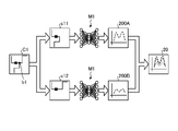
- the complex circuit C1 can be obtained by synthesizing the simple circuit c11 and the simple circuit c12, and the complex circuit C1 can be obtained by synthesizing the EMI strength 200A of the simple circuit c11 and the EMI strength 200B of the simple circuit c12. EMI strength 20 is obtained.
- FIG. 3 is a diagram showing an example of a machine learning method of an EMI prediction model.
- the training data set DS1 is used for machine learning of the EMI prediction model M1.
- the training data set DS1 is a set of training data in which the circuit information of the simple circuits c11 to cN and the EMI intensities 400A to 400N observed in each of the simple circuits c11 to cN are associated with each other.
- the "circuit information” referred to here may include information on the network of elements included in the electronic circuit, for example, a netlist.
- the "EMI intensity” referred to here may be, as an example, a distribution of EMI intensity in a specific frequency domain, a so-called EMI spectrum.
- the EMI intensity 300A is output from the EMI prediction model m1.
- the parameters of the EMI prediction model m1 are updated based on the loss between the EMI strengths of 300B to 300N, which is the output of the EMI prediction model m1, and the EMI strengths of 400A to 400N of the correct label.
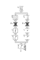
- FIG. 4 is a diagram showing an example of EMI prediction of a complicated circuit.
- FIG. 4 shows, as an example, an example of predicting the EMI intensity of the complex circuit C1 using the trained EMI prediction model M1 shown in FIG.
- the complex circuit C1 is divided into the simple circuit c11 and the simple circuit c12 with the branch point b1 as a boundary.
- the EMI prediction of the simple circuit c11 and the EMI prediction of the simple circuit c12 are performed in parallel. That is, by inputting the circuit information of the simple circuit c11 into the EMI prediction model M1, the estimated value 200A of the EMI intensity can be obtained as the output of the EMI prediction model M1.
- the estimated value 200B of the EMI intensity can be obtained as the output of the EMI prediction model M1.
- the estimated value 20 of the EMI intensity of the complex circuit C1 is obtained.
- EMI prediction of a complicated circuit can be realized by synthesizing the result of EMI prediction of a simple circuit by the EMI prediction model M1 for a simple circuit. Therefore, according to the advanced technology 1, the training data of the complicated circuit can be reduced. Further, in the advanced technology 1, the effect of reducing the number of training data increases as the domain of the EMI prediction model has more branch patterns of the circuit line.
- the circuit having an element having an LCR element such as an inductor (L), a capacitor (C), and a resistor (R) has a pattern in which the current is reflected by the element and a pattern in which the current is not reflected by the element.
- L inductor
- C capacitor
- R resistor
- One of the points of interest is the point that can be expressed by the combination of the above two points.
- the current component reflected by the element may be described as “reflection component”
- the current component not reflected by the element may be described as “non-reflection component”. ..
- the circuit with elements is divided into a circuit equivalent to reflection and a circuit equivalent to non-reflection.
- the "circuit equivalent to reflection” here is an element under the condition that the ratio of the reflection component and the non-reflection component is 1: 0, in other words, the non-reflection component is not observed and only the reflection component is observed. It refers to a circuit whose wiring is the line of the part where the current is observed in the wiring of the circuit.
- the “circuit equivalent to non-reflection” is an element under the condition that the ratio of the reflection component and the non-reflection component is 0: 1, that is, the condition that the reflection component is not observed and only the non-reflection component is observed. Yes Refers to a circuit in which the wiring of the circuit where the current is observed is the wiring.
- the explanatory variable of the EMI prediction model m2 can be a current distribution calculated from the circuit information of the circuit corresponding to reflection or the circuit information of the circuit corresponding to non-reflection.
- the "circuit information" referred to here may include information on the circuit network of the elements included in the electronic circuit, for example, a netlist, as well as physical property values of each element, such as resistance value, inductance, and capacitance.
- all the current distributions calculated for each frequency component included in the frequency domain can be used for machine learning of the EMI prediction model m2, but the details will be described later, but the resonance frequency is represented as the current distribution representing the frequency domain.
- a current distribution can be used.
- the parameters of the EMI prediction model m2 are updated based on. This gives the EMI prediction model M2 in which only the reflection-equivalent circuit and the non-reflection-equivalent circuit are trained.
- the following reference is made as the reference data referred to at the time of EMI prediction of the circuit with elements. Data is generated.
- a look-up table or a function in which the correspondence between the physical property value of the element arranged in the circuit with the element and the ratio of the reflective component and the non-reflective component can be used can be used.
- reflection occurs in a region where the value of the inductor (L) is extremely large, a region where the value of the capacitor (C) is extremely small, and a region where the value of the resistor (R) is extremely large.
- the reflection becomes sufficiently small.
- the physical characteristic value of the element in which the ratio of the reflective component and the non-reflective component is 1: 0 and the physical characteristic value of the element in which the ratio of the reflective component and the non-reflective component is 0: 1 are searched for.
- the capacitance of the capacitor (C) is 1 nF, no reflective component is observed, and only a non-reflective component is observed.
- the capacitance "1nF" of the capacitor (C) is associated with the reflective component "0" and the non-reflective component "1".
- the capacitance of the capacitor (C) is 1 pF
- the reflective component and the non-reflective component are observed at the same ratio.
- the capacitance "1pF” of the capacitor (C) is associated with the reflective component "0.5” and the non-reflective component "0.5".
- the capacitance of the capacitor (C) is 100 fF
- the non-reflective component is not observed and only the reflected component is observed.
- the capacitance "1fF” of the capacitor (C) is associated with the reflective component "1" and the non-reflective component "0".
- the ratio of the reflective component and the non-reflective component corresponding to 1 pF in the capacitance range of the capacitor (C) from 100 fF to 1 nF is given as an example, but any number of corresponding relationships can be used. May be defined.
- FIG. 5 is a diagram showing an example of EMI prediction of a circuit with elements.
- FIG. 5 shows, as an example, an example of predicting the EMI intensity of the circuit C2 with elements using the trained EMI prediction model M2.
- the component ratio "0.5: 0.5" is referenced from the reference data.
- the circuit C2 with an element is divided into a circuit c21 corresponding to reflection and a circuit c22 corresponding to non-reflection.
- the EMI prediction of the circuit c21 corresponding to the reflection and the EMI prediction of the circuit c22 corresponding to the non-reflection are performed in parallel. That is, the current distribution I1 of the circuit c21 corresponding to the reflection is calculated by inputting the circuit information of the circuit c21 corresponding to the reflection into the circuit simulator. By inputting the current distribution I1 of the circuit c21 corresponding to the reflection calculated in this way to the EMI prediction model M2, the estimated value 210A of the EMI intensity can be obtained as the output of the EMI prediction model M2. Further, the current distribution I2 of the circuit c22 corresponding to non-reflection is calculated by inputting the circuit information of the circuit c22 corresponding to non-reflection into the circuit simulator.
- the estimated value 210B of the EMI intensity can be obtained as the output of the EMI prediction model M2.
- the estimated EMI intensity 210A and the estimated EMI intensity 210B are combined according to the ratio of the reflective component and the non-reflective component referred to from the reference data "0.5: 0.5", whereby the circuit C2 with an element is used.
- the estimated value 21 of the EMI intensity of is obtained.
- the EMI prediction of the circuit with elements can be realized by synthesizing the EMI prediction results of the circuit equivalent to reflection and the circuit equivalent to non-reflection. Therefore, according to the advanced technology 2, it is possible to reduce the training data of the circuit other than the circuit corresponding to the reflection and the circuit corresponding to the non-reflection per the circuit with one element. Further, the advanced technology 2 has a higher effect of reducing the number of training data in the domain of the EMI prediction model having more patterns of elements arranged in the circuit and their physical property values.
- the "board characteristic” here refers to the characteristics related to the substrate on which the circuit is printed, such as the line width (line width), the substrate thickness (layer thickness), and the type of substrate resin (dielectric constant). If at least one of the substrate characteristics exemplified here changes, the EMI also changes even if the other substrate characteristics are the same.
- FIG. 6 is a diagram showing an example of variations in substrate characteristics.
- FIG. 6 illustrates a top view of the substrate BP11 and the substrate BP12 having different line widths (line widths) as an example of variations in substrate characteristics.
- line widths line widths
- FIG. 6 between the substrate BP11 and the substrate BP12, the line L11 and the line L12 having the same shape are printed, but the line widths of the line L11 and the line L12 are different.
- the electrical characteristics also change between the substrate BP11 and the substrate BP12, so that the EMI of the substrate BP11 and the substrate BP12 also changes.
- FIG. 7 is a diagram showing another example of variations in substrate characteristics.
- FIG. 7 illustrates cross-sectional views of a substrate BP21 and a substrate BP22 having different substrate thicknesses (layer thicknesses) as an example of variations in substrate characteristics.
- the line width is the same between the line L211 and the line L212 of the substrate BP21 and the line L221 and the line L222 of the substrate BP22, and the print pattern is the same, while the layer thickness W21 and The layer thickness W22 is different.
- the electrical characteristics also change between the substrate BP21 and the substrate BP22, so that the EMI of the substrate BP21 and the substrate BP22 also changes.
- substrate characteristics such as the type of substrate resin (dielectric constant).
- the type of substrate resin there are variations such as a paper phenol substrate (FR-1, FR-2), a glass epoxy resin substrate (FR-4, FR-5), and a glass composite substrate (CEM-3). .. If the type of these substrate resins is different, the dielectric constant is also different, so that the EMI also changes.
- the division and composition exemplified in the advanced technology 1 and the advanced technology 2 only support the reduction of the variation of the training data regarding the branch pattern of the line and the physical property value pattern of the element on the circuit. Therefore, it is difficult to apply the advanced technology 1 and the advanced technology 2 to the reduction of the variation of the training data regarding the substrate characteristics.
- the training data generation function classifies circuit groups having the same circuit shape based on the characteristic impedance, selects a part of the plurality of circuits classified into the same group, and selects the rest. Delete to generate training data for machine learning of the EMI prediction model.
- circuits with different substrate characteristics but common current distribution and EMI can be identified from the characteristic impedance of the circuit. That is, the line width, layer thickness and dielectric constant determine the characteristic impedance of the line, that is, the resistance value in the AC circuit. Such characteristic impedance determines the current distribution flowing through the circuit. In addition, the current distribution determines the EMI emitted from the circuit. Therefore, even if the board characteristics are different, if the characteristic impedance of the circuit is the same, the current distribution and the EMI will be the same.
- FIG. 8 is a diagram showing one aspect of the relationship between the characteristic impedance and the EMI.
- FIG. 8 illustrates two board characteristic parameter sets ps1 and ps2 for circuits having the same circuit shape.
- the substrate characteristic parameter set ps1 includes a line width “0.5 mm”, a layer thickness “0.2 mm”, an electrode thickness “0.01 mm”, a relative permittivity “3.0”, and a frequency “. It includes four board characteristic parameters of "1 GHz”.
- the substrate characteristic parameter set ps1 can be schematically modeled as shown in the substrate BP31 shown in FIG. By inputting the circuit information of the substrate BP31 into the circuit simulator, the current distribution I31 and the EMI intensity 310 of the substrate BP31 can be calculated.
- the substrate characteristic parameter set ps2 includes four line widths "1.0 mm”, layer thickness "0.4 mm”, electrode thickness "0.02 mm”, relative permittivity "3.0”, and frequency "1 GHz”. Includes board characteristic parameters.
- the substrate characteristic parameter set ps2 can be schematically modeled as shown in the substrate BP32 shown in FIG. By inputting the circuit information of the substrate BP32 into the circuit simulator, the current distribution I32 and the EMI intensity 320 of the substrate BP32 can be calculated.
- both the substrate BP31 and the substrate BP32 have the same characteristic impedance of 49.5 ⁇ .
- the current distributions I31 and EMI310 and the current distributions I32 and EMI320 are the same between the substrate BP31 and the substrate BP32. Therefore, under the condition that the explanatory variable of the EMI prediction model is the current distribution, the training data corresponding to each circuit of the substrate BP31 and the substrate BP32 can be regarded as existing at the same position in the feature space. Therefore, it is clear that even if the training data corresponding to one of the substrate BP31 and the substrate BP32 is deleted, the accuracy of the EMI prediction of the EMI prediction model is not adversely affected.
- some of the circuits in the group having the same characteristic impedance are selected, and the rest are deleted.
- the number of circuits having a common characteristic impedance is M
- a maximum of M-1 can be deleted by selecting at least one of the M circuits.
- one of the M circuits having the same characteristic impedance will be selected and the remaining M-1 will be deleted.
- the number of selected circuits and the number of circuits to be deleted will be described. The number can be set arbitrarily.
- FIG. 9 is a diagram showing an example of filtering.
- FIG. 9 shows a schematic diagram of a circuit in which different board characteristic parameters are listed with the same circuit shape, the characteristic impedance calculated from each circuit, and whether or not the training data corresponding to each circuit is excluded from the data set. The correspondence with the filtering result indicating whether or not is shown in a table format.
- the characteristic impedances of the two circuits of the substrate BP41 and the substrate BP46 match.
- the training data corresponding to the circuit of the board BP41 is selected as one of the sets of training data, and the training data corresponding to the circuit of the board BP46 is deleted from the set of training data.
- the training data corresponding to the circuits of the substrate BP42 to the substrate BP45 is selected as one of the set of training data.
- the training data generation function features a current distribution by selecting some circuits from a plurality of circuits having the same circuit shape, different board characteristics, and similar characteristic impedances. Generate training data to be used for training the EMI prediction model as a quantity. Therefore, the number of training data can be reduced because the training data of the deleted circuit is not generated. Therefore, according to the training data generation function according to the present embodiment, it is possible to reduce the variation of the training data regarding the substrate characteristics.
- FIG. 1 schematically shows a block corresponding to a function of the server device 10.
- the server device 10 has a communication interface unit 11, a storage unit 13, and a control unit 15.
- FIG. 1 only shows an excerpt of the functional part related to the above data generation function, and the functional part other than the figure, for example, the functional part that the existing computer is equipped with by default or as an option is a server. It may be provided in the device 10.
- the communication interface unit 11 corresponds to an example of a communication control unit that controls communication with another device, for example, a client terminal 30.
- the communication interface unit 11 can be realized by a network interface card such as a LAN card.
- the communication interface unit 11 receives a request for training data generation and various user settings related to the training data generation function from the client terminal 30. Further, the communication interface unit 11 outputs a set of training data generated by the training data generation function, a trained EMI prediction model, and the like to the client terminal 30.
- the storage unit 13 is a functional unit that stores various types of data.
- the storage unit 13 is realized by storage, for example, internal, external or auxiliary storage.
- the storage unit 13 stores the circuit information group 13A, the training data set 13B, and the model data 13M.
- the storage unit 13 can store various data such as account information of the user who receives the training data generation function. The explanation of each data of the circuit information group 13A, the training data set 13B, and the model data 13M will be described later together with the explanation of the process in which the reference or generation is performed.
- the control unit 15 is a processing unit that controls the entire server device 10.
- the control unit 15 is realized by a hardware processor.
- the control unit 15 includes a setting unit 15A, a calculation unit 15B, a classification unit 15C, a selection unit 15D, a generation unit 15E, and a training unit 15F.
- the setting unit 15A is a processing unit that sets various parameters related to the training data generation function.
- the setting unit 15A can start the operation when the request for training data generation is received from the client terminal 30.
- the setting unit 15A sets the frequency f of the frequency domain to be calculated for the characteristic impedance from the aspect of classifying the circuits based on the characteristic impedance, for example, evaluating the similarity between the circuits by clustering.
- the setting unit 15A sets a threshold value Th to be compared with the distance d between clusters in the clustering of circuits based on the characteristic impedance.
- the user settings received via the client terminal 30 may be applied to these frequencies f and the threshold value Th, or the system settings determined by the designer of the training data generation function and the like may be applied. ..
- the calculation unit 15B is a processing unit that calculates the characteristic impedance of the circuit.
- the calculation unit 15B refers to the circuit information group 13A stored in the storage unit 13.
- the circuit information group 13A is a set of circuit information.
- circuit information there is circuit connection information such as a netlist used in a circuit simulator such as SPICE (Simulation Program with Integrated Circuit Emphasis).
- circuit connection information can be acquired by importing from a design support program such as a CAD (Computer-Aided Design) system.
- the calculation unit 15B fluctuates the numerical value within the range assigned to the board characteristic parameter for each board characteristic parameter for each circuit shape defined by such circuit information.
- the calculation unit 15B comprehensively sets the numerical values within the range assigned as variations for each board characteristic parameter, for example, the numerical values used in the history of the circuit design of the same domain. As a result, a plurality of training data candidate circuits having the same circuit shape but different board characteristics are listed.
- FIG. 10 is a diagram showing an example of a circuit enumeration method.
- FIG. 10 shows an excerpt of an example in which the circuit information 13A1 is used in the circuit information group 13A.
- n training data candidate circuits corresponding to the board characteristic parameter sets PS1 to PSn are listed.
- the line width "W11 (mm)”, the layer thickness "h11 (mm)", the electrode thickness "t11 (mm)", and the relative permittivity "3.0 GHz” are 4
- a circuit of training data candidates with two substrate characteristic parameters is defined.
- the line width "W12 (mm)", the layer thickness "h12 (mm)”, the electrode thickness “t12 (mm)” and the relative permittivity "3.0 GHz” are 4 A circuit of training data candidates with two substrate characteristic parameters is defined.
- the line width "W1n (mm)”, the layer thickness "h1n (mm)”, the electrode thickness "t1n (mm)” and the relative permittivity "3.0 GHz” 4 A circuit of training data candidates with two substrate characteristic parameters is defined.
- the calculation unit 15B sets a dividing line for dividing the circuit line of each training data candidate with the point where the board characteristic parameter is discontinuous among the circuits of the plurality of training data candidates enumerated in this way as a boundary. do. Then, the calculation unit 15B divides the circuit line of each training data candidate circuit according to the dividing line set earlier. As a result, a partial line in which the line is divided by the dividing line is obtained for each circuit of the training data candidate.
- FIG. 11 is a diagram showing an example of a method of setting a dividing line of a line.
- FIG. 11 schematically shows the circuits TR1 to TRn of n training data candidates corresponding to the n board characteristic parameter sets PS1 to PSn shown in FIG. Further, FIG. 11 shows an example in which the dividing line is set by taking the line width as an example among the substrate characteristic parameters.
- the dividing line dl1 is set at the boundary where the line width changes on the line of the training data candidate circuit TR1.
- the dividing line dl2 is set with a portion where the line width changes on the line of the training data candidate circuit TR2 as a boundary.
- the dividing line dl3 is set at the boundary where the line width changes on the line of the training data candidate circuit TRn.
- the lines of the training data candidate circuits TR1 to TRn are divided according to these dividing lines dl1 to dl3.
- the lines of the circuits TR1 to TRn of the training data candidate are divided into partial lines x1 to x4.
- FIG. 11 shows excerpts of the partial lines x1 to x4 of the training data candidate circuits TRn, but the same number of circuits of other training data candidates, that is, four partial lines x1 to x4. It is divided.
- the calculation unit 15B calculates the characteristic impedance for each training data candidate circuit according to the following equation (1).
- equation (1) “w” indicates the line width, “h” indicates the layer thickness, and “t” indicates the electrode thickness.
- “ ⁇ r” in the following equation (1) refers to the relative permittivity and is a function of frequency.
- the substrate characteristic parameters of the line width, the layer thickness, the electrode thickness, and the relative permittivity are input for each of the partial lines x1 to x4 of the circuits TR1 to TRn of the training data candidate.
- the frequency set by the setting unit 15A is used for the relative permittivity.
- the characteristic impedance is calculated for each of the partial lines x1 to x4.
- the characteristic impedance vector Z 0 shown in the following equation (2) can be obtained.
- the notation of the characteristic impedance vector Z 0 mentioned here is a normal font, but it may be expressed in bold or double lines representing the vector.
- the classification unit 15C is a processing unit that classifies circuits of training data candidates based on the characteristic impedance calculated by the calculation unit 15B. As an example, the classification unit 15C calculates the Euclidean distance of the characteristic impedance vector Z 0 for each pair of circuits of training data candidates. For example, when n training data candidate circuits TR1 to TRn are listed, the number of Euclidean distances corresponding to the combination nC2 obtained by extracting two from the n training data candidate circuits TR1 to TRn. Is calculated. Then, the classification unit 15C executes clustering of the training data candidate circuits using the two Euclidean distances of nC calculated for each pair of training data candidate circuits.
- the clusters that minimize the distance d between the clusters are recursively merged from the initial state in which all the clusters are circuits of single training data candidates. Processing is started. Then, the classification unit 15C repeats the process of merging the clusters in which the distance d between the clusters is within the threshold value Th set by the setting unit 15A.
- the training data candidate circuits obtained by such merging are identified as the same group.
- the selection unit 15D is a processing unit that selects one or a plurality of training data candidate circuits from a plurality of training data candidate circuits classified into the same group by the classification process by the classification unit 15C.
- the selection unit 15D selects at least one of the M and at most M-1. Individuals can be deleted.
- an example is given in which one of the circuits of M training data candidates classified in the same group is selected and the remaining M-1 circuits are deleted.
- the number and the number of circuits to be deleted can be set arbitrarily. For example, it is possible to select a maximum of M-1 training data candidate circuits among the M training data candidate circuits and delete a minimum of one training data candidate circuit.
- the generation unit 15E is a processing unit that generates training data for machine learning based on the circuit of one or more training data candidates selected by the selection unit 15D. As an example, the generation unit 15E adds the board characteristic parameter set of the training data candidate circuit to the circuit connection information of the training data candidate circuit selected by the selection unit 15D, the physical property value of the element, and the like. After that, the generation unit 15E calculates the current distribution and the EMI intensity in the circuit of the training data candidate by inputting the circuit information to which the board characteristic parameter set is added to the circuit simulator. For example, the generation unit 15E can calculate the current distribution and the EMI intensity by inputting the circuit information into the circuit simulator operating on the server device 10.
- the generation unit 15E can also make a calculation request for the current distribution and the EMI intensity by using an API (Application Programming Interface) published by an external device, a service, or software that executes the circuit simulator. After that, the generation unit 15E generates training data in which the current distribution and the EMI intensity are associated with each other.
- API Application Programming Interface
- the circuit simulator calculates the current distribution for each frequency component included in a specific frequency domain.
- a current distribution image of the circuit calculated by the circuit simulator for example, a current distribution image in which the intensity of the current flowing on the substrate surface is mapped on a two-dimensional map can be obtained for each frequency component.
- the generation unit 15E identifies one or a plurality of resonance frequencies at which the maximum value of the current distribution calculated for each frequency component has a maximum.
- the generation unit 15E processes the pixel values of the pixels included in the current distribution image corresponding to the resonance frequency based on the distance from the line of each pixel from the aspect of approximating the near field of the electronic circuit. To execute. For example, as the current flowing on the line increases, the shading value approaches the upper limit value, for example, 255 corresponding to white, while as the current decreases, the shading value approaches the lower limit value, for example, 0 corresponding to black.
- the current distribution image generated by this is taken as an example. In this case, as the distance from the line of the pixel included in the current distribution image becomes smaller, the shift amount for shifting the shading value of the pixel to the upper limit value side is set larger.
- the shift amount for shifting the shading value of the pixel to the lower limit value side is set smaller.
- shifting the shading value of the pixels of the current distribution image according to such a shift amount it is possible to obtain a current distribution image in which the intensity of the current is emphasized according to the distance from the line.
- the distance from the line drawn as a 1-pixel line drawing is calculated for each pixel regardless of the size of the line width defined in the board characteristic parameter set. Not limited to this.
- the distance from the line drawn according to the line width defined in the board characteristic parameter set can be calculated for each pixel.
- the generation unit 15E generates training data in which the resonance frequency and current distribution image and the EMI intensity are associated with each other.
- the resonance frequency which is a scalar value
- the resonance frequency is converted into a matrix that can be input to a standard neural network as an example of the EMI prediction model.
- a matrix corresponding to the two-dimensional array of the current distribution image is generated from the aspect of unifying the matrix of each channel to the same type.
- the value of the resonance frequency is embedded in each element of the matrix. Training data in which the matrix and the current distribution image (matrix) in which the resonance frequency generated in this way is embedded and the EMI intensity which is the correct label are associated with each other is generated.
- the generation unit 15E registers the set of the training data generated for each circuit information in the storage unit 13 as the training data set 13B. do.
- the training unit 15F is a processing unit that trains an EMI prediction model using training data for machine learning.
- the training unit 15F may use the training unit 15F. Perform the following processing. That is, the training unit 15F trains the EMI prediction model with the current distribution of the training data included in the training data set 13B as the feature quantity and the EMI intensity as the objective variable.
- the generation unit 15E inputs the resonance frequency corresponding to the input data of the channel 1 and the current distribution image corresponding to the input data of the channel 2 into the EMI prediction model.
- an estimated value of EMI intensity is obtained as the output of the EMI prediction model.
- the training unit 15F updates the parameters of the EMI prediction model based on the loss between the estimated value of the EMI intensity output by the EMI prediction model and the EMI intensity of the correct label. This gives a trained EMI prediction model.
- model data 13M The data related to the trained EMI prediction model obtained in this way is stored in the storage unit 13 as model data 13M.
- the model data 13M includes the layer structure of the machine learning model such as neurons and synapses of each layer of the input layer, the hidden layer, and the output layer, and the weights and biases of each layer.
- Machine learning model parameters may be included.
- model providing service may be performed by providing the model data of the trained EMI prediction model to the client terminal 30, or the EMI prediction for predicting the EMI intensity of the circuit using the trained EMI prediction model. Services may be provided.
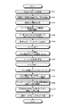
- FIG. 12 is a flowchart showing the procedure of the training data generation process according to the first embodiment. As one aspect, this process can be started when a request for training data generation is received from the client terminal 30.
- the setting unit 15A sets various parameters such as the frequency f for which the characteristic impedance is calculated in the frequency domain and the threshold value Th to be compared with the distance d between the clusters in the clustering of the circuit based on the characteristic impedance. Set (step S101).
- the calculation unit 15B covers and sets the numerical values within the range assigned as variations of the board characteristic parameters for each circuit shape determined by the circuit information included in the circuit information group 13A, thereby n training data.
- the candidate circuits TR1 to TRn are listed (step S102).
- the calculation unit 15B divides the line of the circuit of each training data candidate with the point where the substrate characteristic parameter is discontinuous among the circuits of the plurality of training data candidates listed in step S102 as a boundary. Is set (step S103).
- the calculation unit 15B starts the loop process 1 that repeats the processes of steps S104 and S105 for the number of times corresponding to the number of circuits TR1 to TRn of the training data candidates listed in step S102.
- loop processing may be performed in parallel for each of the training data candidate circuits TR1 to TRn.
- the calculation unit 15B substitutes the board characteristic parameter into the above equation (1) for each partial line in which the line of the training data candidate circuit is divided by the dividing line set in step S103, thereby performing the characteristic impedance. Calculate (step S104).
- the calculation unit 15B creates the characteristic impedance vector Z 0 shown in the above equation (2) by vectorizing the characteristic impedance calculated for each partial line in step S104 (step S105).
- the characteristic impedance vector Z 0 can be obtained for each of the training data candidate circuits TR1 to TRn. Then, when the loop process 1 is completed, the classification unit 15C extracts two from the circuits TR1 to TRn of the n training data candidates listed in step S102, and the number of times corresponding to the combination nC2 obtained. , The loop process 2 that repeats the process of step S106 is started.
- the classification unit 15C calculates the Euclidean distance of the characteristic impedance vector Z0 with respect to the pair of circuits of the two training data candidates (step S106). By repeating the loop process 2 corresponding to step S106, the Euclidean distance can be obtained for each pair of circuits of training data candidates.
- the classification unit 15C executes clustering of the training data candidate circuits using the two Euclidean distances of nC calculated for each pair of training data candidate circuits in step S106 (. Step S107).
- the classification unit 15C identifies the clusters in which the distance d between the clusters obtained by the clustering in step S107 is within the threshold value Th set in step S101 as the same group (step S108).
- the selection unit 15D selects one training data candidate circuit from the training data candidate circuits classified in the same group and deletes the remaining training data candidate circuits (step S109).
- the generation unit 15E generates training data for machine learning by associating the current distribution calculated by inputting the circuit information of the training data candidate circuit selected in step S109 into the circuit simulator and the EMI intensity. (Step S110).
- the training unit 15F trains the EMI prediction model using the current distribution of the training data generated in step S110 as a feature quantity and the EMI intensity as an objective variable (step S111). This gives a trained EMI prediction model.
- the training data generation function selects a part of the circuits having the same circuit shape, different board characteristics, and similar characteristic impedances to obtain the current distribution. Generate training data to be used for training the EMI prediction model as a feature quantity. Therefore, the number of training data can be reduced because the training data of the deleted circuit is not generated. Therefore, according to the training data generation function according to the present embodiment, it is possible to reduce the variation of the training data regarding the substrate characteristics.
- Example 1 an example in which filtering based on clustering is performed on circuits of a plurality of training data candidates having the same circuit shape but different board characteristics is given, but filtering may be performed according to criteria other than clustering. can.
- the characteristic impedance of the circuit line may be designed to take a specific value according to the characteristics of the domain to which the task of the EMI prediction model is applied. Focusing on this point, the range assigned as a variation of the board characteristic parameter is narrowed down to the range of the characteristic impedance value set based on the domain to be predicted. As a result, the number of training data can be further reduced.
- FIG. 13 is a diagram showing an application example of filtering.
- FIG. 13 shows a schematic diagram of circuits of a plurality of training data candidates, a correspondence relationship between the characteristic impedance, the filtering result based on the domain to be predicted, the filtering result based on clustering, and the design result of the training data set. Shown in format. Further, in FIG. 13, an example is given in which the value of the characteristic impedance corresponding to the domain to be predicted is set to 50 ⁇ and narrowed down to the range within ⁇ 5 ⁇ from 50 ⁇ .
- the characteristic impedance values of the three circuits of the substrate BP42, the substrate BP43, and the substrate BP45 are based on the domain to be predicted. It is out of the set range of 50 ⁇ ⁇ 5 ⁇ . In this case, the circuits of the three training data candidates of the substrate BP42, the substrate BP43, and the substrate BP45 are deleted. Further, the two circuits of the substrate BP41 and the substrate BP46 are clustered into the same group.
- the training data candidate circuit corresponding to the board BP41 is selected, and the training data candidate circuit corresponding to the board BP46 is deleted from the training data set.
- the training data candidate circuits corresponding to the substrate BP41 and the substrate BP44 are selected as one of the training data sets.
- the number of training data can be further reduced by performing filtering based on the domain to be predicted. That is, in the example shown in FIG. 13, the three circuits of the substrate BP42, the substrate BP43, and the substrate BP45 can be reduced from the training data set as compared with the example shown in FIG.
- each component of each of the illustrated devices does not necessarily have to be physically configured as shown in the figure. That is, the specific form of distribution / integration of each device is not limited to the one shown in the figure, and all or part of them may be functionally or physically distributed / physically in any unit according to various loads and usage conditions. Can be integrated and configured.
- the setting unit 15A, the calculation unit 15B, the classification unit 15C, the selection unit 15D, the generation unit 15E, or the training unit 15F may be connected via a network as an external device of the server device 10.
- another device has a setting unit 15A, a calculation unit 15B, a classification unit 15C, a selection unit 15D, a generation unit 15E, or a training unit 15F, respectively, and by being connected to a network and cooperating with each other, the above server device 10 can be used.
- the function may be realized.
- FIG. 14 is a diagram showing an example of computer hardware configuration.
- the computer 100 has an operation unit 110a, a speaker 110b, a camera 110c, a display 120, and a communication unit 130. Further, the computer 100 has a CPU 150, a ROM 160, an HDD 170, and a RAM 180. Each of these 110 to 180 parts is connected via the bus 140.
- a CPU is taken as an example of a hardware processor, but the present invention is not limited to this. That is, it is not limited to a general-purpose processor such as a CPU or MPU, but may be a DLU (Deep Learning Unit), a GPGPU (General-Purpose computing on Graphics Processing Units), a GPU cluster, or the like.
- a general-purpose processor such as a CPU or MPU, but may be a DLU (Deep Learning Unit), a GPGPU (General-Purpose computing on Graphics Processing Units), a GPU cluster, or the like.
- the HDD 170 has a training data generation program 170a that exhibits the same functions as the setting unit 15A, the calculation unit 15B, the classification unit 15C, the selection unit 15D, and the generation unit 15E shown in the first embodiment. Is remembered.
- the training data generation program 170a may be integrated or separated in the same manner as the components of the setting unit 15A, the calculation unit 15B, the classification unit 15C, the selection unit 15D, and the generation unit 15E shown in FIG. That is, not all the data shown in FIG. 1 may be stored in the HDD 170, and the data used for processing may be stored in the HDD 170.
- the CPU 150 reads the training data generation program 170a from the HDD 170 and then deploys it to the RAM 180.
- the training data generation program 170a functions as the training data generation process 180a as shown in FIG.
- the training data generation process 180a expands various data read from the HDD 170 into the area allocated to the training data generation process 180a in the storage area of the RAM 180, and executes various processes using the expanded various data. ..
- the process shown in FIG. 12 is included.
- the CPU 150 not all the processing units shown in the first embodiment need to operate, and it is sufficient that the processing units corresponding to the processes to be executed are virtually realized.
- the above training data generation program 170a does not necessarily have to be stored in the HDD 170 or ROM 160 from the beginning.
- each program is stored in a "portable physical medium" such as a flexible disk inserted into the computer 100, a so-called FD, a CD-ROM, a DVD disk, a magneto-optical disk, or an IC card. Then, the computer 100 may acquire and execute each program from these portable physical media. Further, each program is stored in another computer or server device connected to the computer 100 via a public line, the Internet, a LAN, a WAN, or the like, and the computer 100 acquires and executes each program from these. You may do it.
Landscapes
- Engineering & Computer Science (AREA)
- Theoretical Computer Science (AREA)
- Physics & Mathematics (AREA)
- Software Systems (AREA)
- Evolutionary Computation (AREA)
- General Engineering & Computer Science (AREA)
- General Physics & Mathematics (AREA)
- Medical Informatics (AREA)
- Computer Vision & Pattern Recognition (AREA)
- Artificial Intelligence (AREA)
- Computer Hardware Design (AREA)
- Data Mining & Analysis (AREA)
- Computing Systems (AREA)
- Mathematical Physics (AREA)
- Geometry (AREA)
- Design And Manufacture Of Integrated Circuits (AREA)
- Semiconductor Integrated Circuits (AREA)
Priority Applications (4)
| Application Number | Priority Date | Filing Date | Title |
|---|---|---|---|
| EP20956677.7A EP4227847A4 (en) | 2020-10-06 | 2020-10-06 | Training data generation program, training data generation method, and training data generation device |
| JP2022554999A JP7416278B2 (ja) | 2020-10-06 | 2020-10-06 | 訓練データ生成プログラム、訓練データ生成方法及び訓練データ生成装置 |
| PCT/JP2020/037829 WO2022074728A1 (ja) | 2020-10-06 | 2020-10-06 | 訓練データ生成プログラム、訓練データ生成方法及び訓練データ生成装置 |
| US18/191,026 US20230237381A1 (en) | 2020-10-06 | 2023-03-28 | Non-transitory computer-readable recording medium storing training data generation program, training data generation method, and training data generation device |
Applications Claiming Priority (1)
| Application Number | Priority Date | Filing Date | Title |
|---|---|---|---|
| PCT/JP2020/037829 WO2022074728A1 (ja) | 2020-10-06 | 2020-10-06 | 訓練データ生成プログラム、訓練データ生成方法及び訓練データ生成装置 |
Related Child Applications (1)
| Application Number | Title | Priority Date | Filing Date |
|---|---|---|---|
| US18/191,026 Continuation US20230237381A1 (en) | 2020-10-06 | 2023-03-28 | Non-transitory computer-readable recording medium storing training data generation program, training data generation method, and training data generation device |
Publications (1)
| Publication Number | Publication Date |
|---|---|
| WO2022074728A1 true WO2022074728A1 (ja) | 2022-04-14 |
Family
ID=81126705
Family Applications (1)
| Application Number | Title | Priority Date | Filing Date |
|---|---|---|---|
| PCT/JP2020/037829 Ceased WO2022074728A1 (ja) | 2020-10-06 | 2020-10-06 | 訓練データ生成プログラム、訓練データ生成方法及び訓練データ生成装置 |
Country Status (4)
| Country | Link |
|---|---|
| US (1) | US20230237381A1 (https=) |
| EP (1) | EP4227847A4 (https=) |
| JP (1) | JP7416278B2 (https=) |
| WO (1) | WO2022074728A1 (https=) |
Cited By (1)
| Publication number | Priority date | Publication date | Assignee | Title |
|---|---|---|---|---|
| WO2025134410A1 (ja) * | 2023-12-19 | 2025-06-26 | 株式会社デンソー | 分析装置、分析プログラム、方法、半導体装置及び半導体ウエハ |
Citations (5)
| Publication number | Priority date | Publication date | Assignee | Title |
|---|---|---|---|---|
| JP2008078392A (ja) * | 2006-09-21 | 2008-04-03 | Sharp Corp | 特性解析方法および装置、異常設備推定方法および装置、上記特性解析方法または異常設備推定方法をコンピュータに実行させるためのプログラム、並びに上記プログラムを記録したコンピュータ読み取り可能な記録媒体 |
| JP2011158373A (ja) | 2010-02-02 | 2011-08-18 | Dainippon Screen Mfg Co Ltd | 自動欠陥分類のための教師データ作成方法、自動欠陥分類方法および自動欠陥分類装置 |
| JP2018194919A (ja) | 2017-05-12 | 2018-12-06 | 富士通株式会社 | 学習プログラム、学習方法及び学習装置 |
| JP2019082874A (ja) * | 2017-10-31 | 2019-05-30 | 株式会社日立製作所 | 設計支援装置及び設計支援システム |
| JP2019101924A (ja) * | 2017-12-06 | 2019-06-24 | 株式会社豊田中央研究所 | 学習装置、電磁波反射特性推定装置、学習プログラム、および電磁波反射特性推定プログラム |
Family Cites Families (9)
| Publication number | Priority date | Publication date | Assignee | Title |
|---|---|---|---|---|
| US10515300B2 (en) | 2016-09-28 | 2019-12-24 | Dell Products, Lp | High speed serial links for high volume manufacturing |
| US20180197110A1 (en) * | 2017-01-11 | 2018-07-12 | Netspeed Systems, Inc. | Metrics to Train Machine Learning Predictor for NoC Construction |
| WO2019127231A1 (en) * | 2017-12-28 | 2019-07-04 | Intel Corporation | Training data generators and methods for machine learning |
| EP3654103A1 (en) * | 2018-11-14 | 2020-05-20 | ASML Netherlands B.V. | Method for obtaining training data for training a model of a semicondcutor manufacturing process |
| US20200166909A1 (en) * | 2018-11-20 | 2020-05-28 | Relativity Space, Inc. | Real-time adaptive control of manufacturing processes using machine learning |
| US12099788B2 (en) * | 2018-11-26 | 2024-09-24 | Agency For Science, Technology And Research | Method and system for predicting performance in electronic design based on machine learning |
| SG11202105436YA (en) * | 2018-11-26 | 2021-06-29 | Agency Science Tech & Res | Method and system for generating training data for a machine learning model for predicting performance in electronic design |
| JP7172612B2 (ja) * | 2019-01-11 | 2022-11-16 | 富士通株式会社 | データ拡張プログラム、データ拡張方法およびデータ拡張装置 |
| US11790139B1 (en) * | 2022-04-18 | 2023-10-17 | Xilinx, Inc. | Predicting a performance metric based on features of a circuit design and explaining marginal contributions of the features to the prediction |
-
2020
- 2020-10-06 JP JP2022554999A patent/JP7416278B2/ja active Active
- 2020-10-06 WO PCT/JP2020/037829 patent/WO2022074728A1/ja not_active Ceased
- 2020-10-06 EP EP20956677.7A patent/EP4227847A4/en active Pending
-
2023
- 2023-03-28 US US18/191,026 patent/US20230237381A1/en active Pending
Patent Citations (5)
| Publication number | Priority date | Publication date | Assignee | Title |
|---|---|---|---|---|
| JP2008078392A (ja) * | 2006-09-21 | 2008-04-03 | Sharp Corp | 特性解析方法および装置、異常設備推定方法および装置、上記特性解析方法または異常設備推定方法をコンピュータに実行させるためのプログラム、並びに上記プログラムを記録したコンピュータ読み取り可能な記録媒体 |
| JP2011158373A (ja) | 2010-02-02 | 2011-08-18 | Dainippon Screen Mfg Co Ltd | 自動欠陥分類のための教師データ作成方法、自動欠陥分類方法および自動欠陥分類装置 |
| JP2018194919A (ja) | 2017-05-12 | 2018-12-06 | 富士通株式会社 | 学習プログラム、学習方法及び学習装置 |
| JP2019082874A (ja) * | 2017-10-31 | 2019-05-30 | 株式会社日立製作所 | 設計支援装置及び設計支援システム |
| JP2019101924A (ja) * | 2017-12-06 | 2019-06-24 | 株式会社豊田中央研究所 | 学習装置、電磁波反射特性推定装置、学習プログラム、および電磁波反射特性推定プログラム |
Non-Patent Citations (1)
| Title |
|---|
| See also references of EP4227847A4 |
Cited By (1)
| Publication number | Priority date | Publication date | Assignee | Title |
|---|---|---|---|---|
| WO2025134410A1 (ja) * | 2023-12-19 | 2025-06-26 | 株式会社デンソー | 分析装置、分析プログラム、方法、半導体装置及び半導体ウエハ |
Also Published As
| Publication number | Publication date |
|---|---|
| JP7416278B2 (ja) | 2024-01-17 |
| US20230237381A1 (en) | 2023-07-27 |
| JPWO2022074728A1 (https=) | 2022-04-14 |
| EP4227847A4 (en) | 2023-11-22 |
| EP4227847A1 (en) | 2023-08-16 |
Similar Documents
| Publication | Publication Date | Title |
|---|---|---|
| Liu et al. | Multiple classifiers combination by clustering and selection | |
| JP6599057B1 (ja) | 設計支援装置、設計支援方法および機械学習装置 | |
| JP2020060877A (ja) | 推定プログラム、推定装置および推定方法 | |
| Hrytsyk et al. | Real-time sensing, reasoning and adaptation for computer vision systems | |
| JP6323333B2 (ja) | 基板設計方法及び設計装置 | |
| WO2019102984A1 (ja) | 学習装置及び学習方法、識別装置及び識別方法、プログラム並びに記録媒体 | |
| KR102464963B1 (ko) | 데이터 기반의 물체 위치 최적화를 위한 강화학습 장치 | |
| JP7416278B2 (ja) | 訓練データ生成プログラム、訓練データ生成方法及び訓練データ生成装置 | |
| JP2006252333A (ja) | データ処理方法、データ処理装置およびそのプログラム | |
| KR20230149554A (ko) | 비전 트랜스포머의 정규화 장치 및 방법 | |
| JP7416279B2 (ja) | 訓練データ生成プログラム、訓練データ生成方法及び訓練データ生成装置 | |
| KR20200052411A (ko) | 영상 분류 장치 및 방법 | |
| CN118228644A (zh) | 数字芯片设计的方法、装置、设备、存储介质和程序产品 | |
| EP3910523B1 (en) | Machine learning program, method and device for estimating the electromagnetic wave radiation situation of an electronic circuit | |
| EP4080398A1 (en) | Emi calculation program, emi calculation method, and emi calculation apparatus | |
| JP2023178008A (ja) | 設計支援装置及び設計支援方法 | |
| CN120317195A (zh) | 一种提高主板散热性能的热仿真分析方法及其系统 | |
| US20240257901A1 (en) | Information processing device, information processing method, and non- transitory computer-readable storage medium stored with information processing program | |
| JP6842436B2 (ja) | 情報処理装置、情報処理方法、及びプログラム | |
| US20190294745A1 (en) | Methods For Converting Circuits In Circuit Simulation Programs | |
| Dervenis et al. | Neural network specialists for inverse spiral inductor design | |
| JP4444140B2 (ja) | 干渉解析方法及び干渉解析装置及び干渉解析プログラム及び干渉解析プログラムを記録した記録媒体 | |
| Le et al. | Length-Dependent Deep Neural Network Based Modeling for High-Speed Channels | |
| JP4202222B2 (ja) | 伝送線路解析方法及び装置 | |
| JP7028332B2 (ja) | パラメタ値付与装置、方法、およびプログラム |
Legal Events
| Date | Code | Title | Description |
|---|---|---|---|
| 121 | Ep: the epo has been informed by wipo that ep was designated in this application |
Ref document number: 20956677 Country of ref document: EP Kind code of ref document: A1 |
|
| ENP | Entry into the national phase |
Ref document number: 2022554999 Country of ref document: JP Kind code of ref document: A |
|
| NENP | Non-entry into the national phase |
Ref country code: DE |
|
| ENP | Entry into the national phase |
Ref document number: 2020956677 Country of ref document: EP Effective date: 20230508 |