WO2022070888A1 - コイル部品、これを含むフィルタ回路、および電子機器 - Google Patents
コイル部品、これを含むフィルタ回路、および電子機器 Download PDFInfo
- Publication number
- WO2022070888A1 WO2022070888A1 PCT/JP2021/033751 JP2021033751W WO2022070888A1 WO 2022070888 A1 WO2022070888 A1 WO 2022070888A1 JP 2021033751 W JP2021033751 W JP 2021033751W WO 2022070888 A1 WO2022070888 A1 WO 2022070888A1
- Authority
- WO
- WIPO (PCT)
- Prior art keywords
- coil
- electrode
- wiring pattern
- capacitor
- component
- Prior art date
- Legal status (The legal status is an assumption and is not a legal conclusion. Google has not performed a legal analysis and makes no representation as to the accuracy of the status listed.)
- Ceased
Links
Images





Classifications
-
- H—ELECTRICITY
- H03—ELECTRONIC CIRCUITRY
- H03H—IMPEDANCE NETWORKS, e.g. RESONANT CIRCUITS; RESONATORS
- H03H7/00—Multiple-port networks comprising only passive electrical elements as network components
- H03H7/01—Frequency selective two-port networks
- H03H7/17—Structural details of sub-circuits of frequency selective networks
- H03H7/1741—Comprising typical LC combinations, irrespective of presence and location of additional resistors
- H03H7/1758—Series LC in shunt or branch path
-
- H—ELECTRICITY
- H03—ELECTRONIC CIRCUITRY
- H03H—IMPEDANCE NETWORKS, e.g. RESONANT CIRCUITS; RESONATORS
- H03H7/00—Multiple-port networks comprising only passive electrical elements as network components
- H03H7/01—Frequency selective two-port networks
- H03H7/0115—Frequency selective two-port networks comprising only inductors and capacitors
-
- H—ELECTRICITY
- H01—ELECTRIC ELEMENTS
- H01F—MAGNETS; INDUCTANCES; TRANSFORMERS; SELECTION OF MATERIALS FOR THEIR MAGNETIC PROPERTIES
- H01F17/00—Fixed inductances of the signal type
- H01F17/0006—Printed inductances
- H01F17/0013—Printed inductances with stacked layers
-
- H—ELECTRICITY
- H01—ELECTRIC ELEMENTS
- H01F—MAGNETS; INDUCTANCES; TRANSFORMERS; SELECTION OF MATERIALS FOR THEIR MAGNETIC PROPERTIES
- H01F27/00—Details of transformers or inductances, in general
- H01F27/28—Coils; Windings; Conductive connections
- H01F27/29—Terminals; Tapping arrangements for signal inductances
- H01F27/292—Surface mounted devices
-
- H—ELECTRICITY
- H03—ELECTRONIC CIRCUITRY
- H03H—IMPEDANCE NETWORKS, e.g. RESONANT CIRCUITS; RESONATORS
- H03H1/00—Constructional details of impedance networks whose electrical mode of operation is not specified or applicable to more than one type of network
- H03H1/02—RC networks, e.g. filters
-
- H—ELECTRICITY
- H03—ELECTRONIC CIRCUITRY
- H03H—IMPEDANCE NETWORKS, e.g. RESONANT CIRCUITS; RESONATORS
- H03H7/00—Multiple-port networks comprising only passive electrical elements as network components
- H03H7/01—Frequency selective two-port networks
- H03H7/17—Structural details of sub-circuits of frequency selective networks
- H03H7/1741—Comprising typical LC combinations, irrespective of presence and location of additional resistors
- H03H7/1791—Combined LC in shunt or branch path
-
- H—ELECTRICITY
- H01—ELECTRIC ELEMENTS
- H01F—MAGNETS; INDUCTANCES; TRANSFORMERS; SELECTION OF MATERIALS FOR THEIR MAGNETIC PROPERTIES
- H01F17/00—Fixed inductances of the signal type
- H01F17/0006—Printed inductances
- H01F17/0013—Printed inductances with stacked layers
- H01F2017/0026—Multilayer LC-filter
-
- H—ELECTRICITY
- H03—ELECTRONIC CIRCUITRY
- H03H—IMPEDANCE NETWORKS, e.g. RESONANT CIRCUITS; RESONATORS
- H03H1/00—Constructional details of impedance networks whose electrical mode of operation is not specified or applicable to more than one type of network
- H03H2001/0021—Constructional details
- H03H2001/0085—Multilayer, e.g. LTCC, HTCC, green sheets
Definitions
- It comprises a second electrode and a third electrode provided on the third surface of the side surface not facing the first surface and electrically connected to the other end of the first coil and the other end of the second coil.
- the opening of the first coil and the opening of the second coil overlap at least partly, the third electrode is connected to the ground via a capacitor, and the first coil is compared with the second coil. And the inductance is small.
- the first coil since the first coil has a smaller inductance than the second coil, it is possible to improve the rise of electric charge supplied from the capacitor connected to the third electrode.
- FIG. It is a schematic diagram which shows the structure of the electronic device which concerns on Embodiment 1.
- FIG. It is a circuit diagram of the filter circuit including the coil component which concerns on Embodiment 1.
- FIG. It is a perspective view of the coil component which concerns on Embodiment 1.
- FIG. It is an exploded plan view which shows the structure of the coil component which concerns on Embodiment 1.
- FIG. It is a figure for demonstrating the combination of the inductance of the coil L1 and the coil L2. It is sectional drawing of the coil component which concerns on Embodiment 1.
- FIG. It is an exploded plan view which shows the structure of the coil component which concerns on Embodiment 2.
- FIG. It is an exploded plan view which shows the structure of the coil component which concerns on Embodiment 3.
- FIG. 1 is a schematic diagram showing a configuration of an electronic device according to the first embodiment.
- the electronic device includes a circuit component 200 mounted on a substrate (not shown) and a filter circuit 100 connecting one end to the circuit component 200.
- the capacitor C1 has one end connected to the electrode 4c and the other end connected to the GND wiring.
- the capacitor C1 is not only a monolithic ceramic capacitor containing BaTiO 3 (barium titanate) as a main component, but also a monolithic ceramic capacitor mainly composed of another material, which is not a monolithic ceramic capacitor, for example, an aluminum electrolytic capacitor or the like.
- the type of capacitor may be used.
- the capacitor C1 has an inductor L3 as a parasitic inductance (equivalent series inductance (ESL)), which is equivalent to a circuit configuration in which the inductor L3 is connected in series with the capacitor C1a.
- the capacitor C1 may further have a circuit configuration in which a parasitic resistance (equivalent series resistance (ESR)) is connected in series to the inductor L3 and the capacitor C1a.
- the coil L1 and the coil L2 are connected to the electrode 4c.
- the coil L1 and the coil L2 are magnetically coupled to generate a negative inductance component.
- the parasitic inductance (inductor L3) of the capacitor C1 can be canceled, and the inductance component of the capacitor C1 can be apparently reduced. That is, the filter circuit 100 composed of the capacitor C1, the coil L1 and the coil L2 suppresses noise in the high frequency band by canceling the parasitic inductance of the capacitor C1 with a negative inductance component due to the mutual inductance of the coil L1 and the coil L2. The effect can be improved.
- the filter circuit 100 since the filter circuit 100 has a circuit configuration in which the coil L1 and the coil L2 are magnetically coupled, the coil L1 always exists between the circuit component 200 and the capacitor C1.
- the inductance of the coil L1 causes the charge to be supplied from the capacitor C1 to the circuit component 200 to rise. Was sometimes delayed.
- FIG. 3 is a perspective view of the coil component 1 according to the first embodiment.
- FIG. 4 is an exploded plan view showing the configuration of the coil component according to the first embodiment.
- FIG. 5 is a diagram for explaining a combination of inductances of the coil L1 and the coil L2.
- FIG. 6 is a cross-sectional view of the coil component 1 according to the first embodiment.
- the short side direction of the coil component 1 is the X direction
- the long side direction is the Y direction
- the height direction is the Z direction.
- the stacking direction of the substrates is the Z direction
- the direction of the arrow indicates the upper layer direction.
- the coil component 1 is composed of a laminated body 3 (prime field) of a ceramic layer in which a plurality of substrates (ceramic green sheets) on which coil wiring is formed are laminated.
- the laminated body 3 has a pair of main surfaces facing each other and side surfaces connecting the main surfaces.
- a plurality of first wiring patterns 10 and a plurality of second wiring patterns 20 are stacked in order from the bottom in parallel with the main surface of the laminated body 3, forming a coil L1 and a coil L2. Therefore, the inductance of the coil L1 and the coil L2 can be controlled by the configuration of the first wiring pattern 10 and the second wiring pattern 20.
- a wiring pattern 20a which is a second wiring pattern 20, is formed on the ceramic green sheet 3a.
- the wiring pattern 20a is formed so as to make one round counterclockwise in the figure along each side from the center of the long side on the lower side in the figure of the ceramic green sheet 3a, and is formed to the lower side of the short side on the left side in the figure.
- Ru An end portion 21 for connecting to the electrode 4b is provided at the start end of the wiring pattern 20a, and a connection portion 56a for connecting to the via conductor 56 is provided at the end end.
- the ceramic green sheet 3b is formed with a wiring pattern 10b which is a first wiring pattern 10 and a wiring pattern 20b which is a second wiring pattern 20.
- the wiring pattern 10b is formed from the left side of the long side on the upper side in the figure to the center of the short side on the right side in the figure of the ceramic green sheet 3b.
- a connecting portion 52b for connecting to the via conductor 52 is provided at the start end of the wiring pattern 10b, and an end portion 31 for connecting to the electrode 4c is provided at the end.
- the wiring pattern 20b is formed from the left side of the long side on the lower side in the figure to the center of the short side on the right side in the figure of the ceramic green sheet 3b.
- a connecting portion 56b for connecting to the via conductor 56 is provided at the start end of the wiring pattern 20b, and an end portion 31 for connecting to the electrode 4c is provided at the end.
- the wiring pattern 20a and the wiring pattern 20b are electrically connected by the via conductor 56 to form the coil L2. Further, in the ceramic green sheets 3b to 3d, the wiring pattern 10b, the wiring pattern 10c, and the wiring pattern 10d are electrically connected by the via conductor 52 to form the coil L1.
- the relationship between the mutual inductance M and the inductances of the coils L1 and L2 will be described.
- M ⁇ k (L1 ⁇ L2) 1/2 when the respective inductances of the coils L1 and L2 are represented by L1 and L2, and the coupling coefficient between the coil L1 and the coil L2 is represented by k.
- the coupling coefficient k 0.5.
- the circuit component 200 when the circuit component 200 is connected to the coil L1 side as described above, it is necessary to reduce the inductance of the coil L1 while maintaining the same mutual inductance M.
- the resistance value from the capacitor C1 to the circuit component 200 is about 1/4. Can be reduced. Further, the inductance from the capacitor C1 to the circuit component 200 is 1.54 nH in total of the inductance of the coil L1 and the inductance of the capacitor C1, which can be reduced to about half as compared with the case where the inductance of the coil L1 is 2.0 nH. Even if the capacitor C1 is simply connected to the circuit component 200, the equivalent series inductance ESL of 1.0 nH exists, so the total inductance of the coil L1 and the capacitor C1 increases to 1.54 nH. Also, the influence of the coil L1 on the charge supply from the capacitor C1 to the circuit component 200 can be significantly reduced.
- each of the plurality of ceramic green sheets 3a to 3d is laminated, and a plurality of ceramic green sheets (dummy layers) having no wiring pattern printed on both upper and lower sides thereof are laminated.
- Stack By crimping a plurality of ceramic green sheets including a dummy layer, an unfired laminated body 3 (ceramic prime field) is formed. The formed laminate 3 is fired, and copper electrodes are baked onto the outside of the fired laminate 3 so as to be conductive with the wiring pattern to form the electrodes 4a to 4d.
- the coil component 1 a plurality of ceramic green sheets forming the wiring of the first wiring pattern 10 constituting the coil L1 and the second wiring pattern 20 constituting the coil L2 are laminated. Therefore, in the coil component 1, the first wiring pattern 10 and the second wiring pattern 20 are arranged so that at least a part of the opening of the coil L1 and the opening of the coil L2 are overlapped when viewed from the main surface direction.
- the magnetic coupling between the coil L1 and the coil L2 fluctuates depending on the degree of overlap between the opening of the coil L1 and the opening of the coil L2.
- the coil component 1 is formed by laminating a plurality of wiring patterns of metal portions and ceramic green sheets of ceramic portions and pressurizing them.
- the laminate 3 may be cracked due to the difference in the compressibility between the metal portion and the ceramic portion during pressurization.
- the laminated body 3 may be cracked due to the difference in heat shrinkage between the metal portion and the ceramic portion during firing.
- the number of wiring patterns in which the end portion 11 for connecting to the electrode 4a is provided in the first wiring pattern 10 is reduced in order to prevent cracking during manufacturing.
- the electrodes in the first wiring pattern 10 or the second wiring pattern 20 are obtained.
- the number of wiring patterns provided with the end 31 for connecting to 4c may be reduced.
- the first wiring pattern 10 of the odd-numbered layers is electrically connected to the electrode 4a.
- the end portion 11 is provided, and the end portion 11 for electrically connecting to the electrode 4a is not provided in the first wiring pattern 10 of the even-numbered layer.
- one main surface of the laminate 3 close to the coil L1 is used as a mounting surface (lower surface in FIG. 6). That is, in the coil component 1, by mounting the coil L1 on the substrate with the side provided with the coil L1 facing downward, the distance from the end portion 11 to the electrode of the substrate via the electrode 4a is the distance from the end portion 21 to the electrode 4b. It becomes shorter than the distance to reach the electrode of the substrate.
- the inductance of the coil L1 Is advantageous in that the resistance value from the coil L1 to the circuit component 200 can be reduced.
- the laminated body 3 is composed of a plurality of laminated insulating layers and has a pair of main surfaces facing each other and four side surfaces connecting the main surfaces.
- a coil L1 composed of a part of a plurality of wiring patterns stacked inside the laminated body 3, a coil L2 provided in a layer different from the coil L1 and composed of a part of a plurality of wiring patterns, and the like.
- An electrode 4a provided on the first surface of the side surface and electrically connected to one end of the coil L1 and an electrode 4a provided on the second surface of the side surface facing the first surface and electrically connected to one end of the coil L2.
- It includes an electrode 4b to be connected and an electrode 4c provided on a third surface of a side surface not facing the first surface and electrically connected to the other end of the coil L1 and the other end of the coil L2.
- the electrode 4c is connected to the ground via the capacitor C1, and the coil L1 has an inductance as compared with the coil L2. Is small.
- the coil component 1 according to the first embodiment has a smaller inductance of the coil L1 than the coil L2, it is possible to improve the rise of the electric charge supplied from the capacitor C1 connected to the electrode 4c.
- one main surface of the laminated body 3 close to the coil L1 is used as the mounting surface.
- the distance from the coil L1 to the electrode of the substrate via the electrode 4a is shorter than the distance from the coil L2 to the electrode of the substrate via the electrode 4b, so that the resistance value from the coil L1 to the circuit component 200 is reduced. Can be reduced.
- At least one of the coil L1 and the coil L2 has a portion in which wiring patterns formed in a plurality of layers are connected in parallel. This makes it possible to reduce the resistance value of the coil having a portion in which a plurality of wiring patterns are connected in parallel.
- the coil L1 has a larger number of layers of wiring patterns connected in parallel than the coil L2. As a result, the coil L1 can have a smaller resistance value than the coil L2.
- the filter circuit 100 includes the coil component 1 described above, and a capacitor C1 connected to an electrode 4c between the coil L1 and the coil L2 of the coil component 1. As a result, the filter circuit 100 can improve the rise of the electric charge supplied from the capacitor C1 to the circuit component 200 connected via the coil L1.
- the electronic device includes a circuit component 200 mounted on a substrate and a filter circuit 100 connecting one end to the circuit component 200.
- the filter circuit 100 includes a coil component 1 and a capacitor C1.
- the coil component 1 is composed of a plurality of laminated insulating layers, and is stacked inside a laminated body 3 having a pair of main surfaces facing each other and four side surfaces connecting the main surfaces.
- a coil L1 composed of a part of a plurality of wiring patterns, a coil L2 provided on a layer different from the coil L1 and formed of a part of a plurality of wiring patterns, and a coil L1 provided on the first surface of a side surface.
- An electrode 4a electrically connected to one end, an electrode 4b provided on the second surface of the side surface facing the first surface and electrically connected to one end of the coil L2, and facing the first surface. It comprises an electrode 4c provided on the third surface of the non-side surface, which is electrically connected to the other end of the coil L1 and the other end of the coil L2.
- the opening of the coil L1 and the opening of the coil L2 overlap at least a part, the electrode 4a is connected to the circuit component 200, and the electrode 4c is connected to the ground via the capacitor C1.
- the coil L1 has a smaller inductance than the coil L2.
- the coil L1 of the coil component 1 since the coil L1 of the coil component 1 has a smaller inductance than the coil L2, it is supplied from the capacitor C1 to the circuit component 200 connected via the coil L1. It is possible to improve the rise of the charged charge.
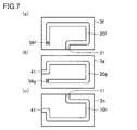
- FIG. 7 is an exploded plan view showing the configuration of the coil component according to the second embodiment.
- the coil component shown in the second embodiment detailed description will not be repeated using the same reference numerals for the same configuration as the coil component 1 according to the first embodiment.
- the coil component shown in the second embodiment can be applied to the filter circuit 100 and the electronic device according to the first embodiment instead of the coil component 1 according to the first embodiment.
- each of the first wiring pattern 10 and the second wiring pattern 20 is wired by printing a conductive paste (Ni paste) on the ceramic green sheets 3f to 3h, which are substrates, by a screen printing method. Form a pattern.
- a conductive paste Ni paste
- a wiring pattern 20f which is a second wiring pattern 20, is formed on the ceramic green sheet 3f.
- the wiring pattern 20f is formed so as to make one round counterclockwise in the figure along each side from the center of the long side on the lower side in the figure of the ceramic green sheet 3f, and is formed to the lower side of the short side on the left side in the figure.
- Ru An end portion 21 for connecting to the electrode 4b is provided at the start end of the wiring pattern 20f, and a connection portion 56f for connecting to the via conductor 56 is provided at the end end.
- a wiring pattern 10h which is the first wiring pattern 10, is formed on the ceramic green sheet 3h.
- the wiring pattern 10h is formed so as to make one round clockwise in the figure along each side from the center of the long side on the upper side in the figure of the ceramic green sheet 3h, and is formed up to the center of the short side on the left side in the figure.
- An end portion 11 for connecting to the electrode 4a is provided at the start end of the wiring pattern 10h, and an end portion 41 for connecting to the electrode 4d is provided at the end end.
- the wiring pattern 20f and the wiring pattern 20g are electrically connected by the via conductor 56 to form the coil L2.
- the ceramic green sheet 3h constitutes the coil L1 with a wiring pattern 10h. Further, the position where the electrode connected between the coil L1 and the coil L2 is pulled out from the electrode 4c to the electrode 4d is changed to reduce the number of turns of the wiring pattern of the coil L1 as compared with the coil L2.
- the winding pattern of the coil L1 is wound as compared with the coil L2. Since the number is small, the inductance and resistance value of the coil L1 can be reduced.
- the inductance and resistance of the coil L1 can be reduced by changing the position where the electrode connected between the coil L1 and the coil L2 is pulled out from the electrode 4c to the electrode 4d, but the capacitor C1 is connected to the electrode 4d. It is necessary to connect the above, and it is necessary to adjust the wiring from the capacitor C1 to the electrode 4d in the filter circuit 100.
- the coil L1 has a smaller number of turns of the wiring pattern than the coil L2.
- the inductance of the coil L1 is smaller than that of the coil L2, so that the rise of the electric charge supplied from the capacitor C1 connected to the electrode 4c can be improved.
- FIG. 8 is an exploded plan view showing the configuration of the coil component according to the third embodiment.
- the coil component shown in the third embodiment detailed description will not be repeated using the same reference numerals for the same configuration as the coil component 1 according to the first embodiment.
- the coil component shown in the third embodiment can be applied to the filter circuit 100 and the electronic device according to the first embodiment instead of the coil component 1 according to the first embodiment.
- each of the first wiring pattern 10 and the second wiring pattern 20 is wired by printing a conductive paste (Ni paste) on the ceramic green sheets 3j to 3l which are substrates by a screen printing method. Form a pattern.
- a conductive paste Ni paste
- a wiring pattern 20j which is a second wiring pattern 20, is formed on the ceramic green sheet 3j.
- the wiring pattern 20j is formed so as to make one round counterclockwise in the figure along each side from the center of the long side on the lower side in the figure of the ceramic green sheet 3j, and is formed to the lower side of the short side on the left side in the figure.
- Ru An end portion 21 for connecting to the electrode 4b is provided at the start end of the wiring pattern 20j, and a connection portion 56j for connecting to the via conductor 56 is provided at the end end.
- the wiring pattern 10k is formed from the left side of the long side on the upper side in the figure to the center of the short side on the right side in the figure of the ceramic green sheet 3k.
- a connection portion 52k for connecting to the via conductor 52 is provided at the start end of the wiring pattern 10k, and an end portion 31 for connecting to the electrode 4c is provided at the end end.
- the wiring pattern 20k is formed from the left side of the long side on the lower side in the figure to the center of the short side on the right side in the figure of the ceramic green sheet 3k.
- a connection portion 56k for connecting to the via conductor 56 is provided at the start end of the wiring pattern 20k, and an end portion 31 for connecting to the electrode 4c is provided at the end end.
- the wiring pattern 10k has a wider wiring width than the wiring pattern 20k.
- a wiring pattern 10l which is the first wiring pattern 10, is formed on the ceramic green sheet 3l.
- the wiring pattern 10l is formed so as to make one round clockwise in the figure along each side from the center of the long side on the upper side in the figure of the ceramic green sheet 3l, and is formed up to the upper side of the short side on the left side in the figure.
- An end portion 11 for connecting to the electrode 4a is provided at the start end of the wiring pattern 10l, and a connection portion 52l for connecting to the via conductor 52 is provided at the end end.
- the wiring pattern 10l has a wider wiring width than the wiring pattern 20j.
- the wiring pattern 20j and the wiring pattern 20k are electrically connected by the via conductor 56 to form the coil L2. Further, in the ceramic green sheets 3k and 3l, the wiring pattern 20k and the wiring pattern 20l are electrically connected by the via conductor 52 to form the coil L1.
- the coil L1 has a wider wiring pattern than the coil L2.
- the inductance and the resistance value of the coil L1 can be reduced by increasing the wiring width of the wiring pattern constituting the coil L1 as compared with the coil L2. can. If the wiring width of the wiring pattern of the coil L1 is relatively thicker than that of the coil L2, the wiring width of the wiring pattern of the coil L2 may be narrowed or the wiring width of the wiring pattern of the coil L1 may be increased. good.
- the wiring width of the wiring pattern configured by the coil L1 is wider than that of the coil L2.
- the inductance of the coil L1 is smaller than that of the coil L2, so that the rise of the electric charge supplied from the capacitor C1 connected to the electrode 4c can be improved.
- the end portion 31 to be connected to the electrode 4c is provided, and the case where the capacitor C1 is connected to the electrode 4c is the configuration of the first connection, the electrode 4d.
- the case where the capacitor C1 is connected to the second connection is used.
- the coil component shown in the fourth embodiment detailed description will not be repeated using the same reference numerals for the same configuration as the coil component 1 according to the first embodiment.
- the coil component shown in the fourth embodiment can be applied to the filter circuit 100 and the electronic device according to the first embodiment instead of the coil component 1 according to the first embodiment.
- FIG. 9 is an exploded plan view showing the configuration of the first connection of the coil component according to the fourth embodiment.
- each of the first wiring pattern 10 and the second wiring pattern 20 is wired by printing a conductive paste (Ni paste) on the ceramic green sheets 3n to 3q which are substrates by a screen printing method. Form a pattern.
- a conductive paste Ni paste
- a wiring pattern 20n which is a second wiring pattern 20, is formed on the ceramic green sheet 3n.
- the wiring pattern 20n is formed so as to make one round counterclockwise in the figure along each side from the center of the long side on the lower side in the figure of the ceramic green sheet 3n, and is formed to the lower side of the short side on the left side in the figure.
- Ru An end portion 21 for connecting to the electrode 4b is provided at the start end of the wiring pattern 20n, and a connection portion 56n for connecting to the via conductor 56 is provided at the end end.
- the wiring pattern 10p which is the first wiring pattern 10 and the wiring pattern 20p which is the second wiring pattern 20 are formed on the ceramic green sheet 3p. ..
- the wiring pattern 10p is formed counterclockwise in the figure from the center of the short side on the right side in the figure to the center of the short side on the left side in the figure along the long side on the upper side in the figure of the ceramic green sheet 3p.
- An end portion 31 for connecting to the electrode 4c is provided at the start end of the wiring pattern 10p, and an end portion 41 for connecting to the electrode 4d is provided at the end end.
- the wiring pattern 20p is formed counterclockwise in the figure from the left side of the long side on the lower side in the figure to the center of the short side on the right side in the figure along the long side on the lower side in the figure of the ceramic green sheet 3p. ..
- a connecting portion 56p for connecting to the via conductor 56 is provided at the start end of the wiring pattern 20p, and an end portion 31 for connecting to the electrode 4c is provided at the end.
- a wiring pattern 10q which is the first wiring pattern 10, is formed on the ceramic green sheet 3q.
- the wiring pattern 10q is formed so as to make one round clockwise in the figure along each side from the center of the long side on the upper side in the figure of the ceramic green sheet 3q, and is formed up to the center of the short side on the left side in the figure.
- An end portion 11 for connecting to the electrode 4a is provided at the start end of the wiring pattern 10q, and an end portion 41 for connecting to the electrode 4d is provided at the end end.
- the wiring pattern 20n and the wiring pattern 20p are electrically connected by the via conductor 56 to form the coil L2. Further, in the ceramic green sheets 3p and 3q, the wiring pattern 10p and the wiring pattern 10q are electrically connected by the electrodes 4d to form the coil L1.
- FIG. 10 is a circuit diagram of a filter circuit including the coil component of the first connection according to the fourth embodiment.
- the wiring pattern 20p which is the second wiring pattern 20 is formed on the ceramic green sheet 3p.
- the wiring pattern 20p is formed counterclockwise in the figure from the left side of the long side on the lower side in the figure to the center of the short side on the left side in the figure along each side of the ceramic green sheet 3p.
- a connecting portion 56p for connecting to the via conductor 56 is provided at the start end of the wiring pattern 20p, and an end portion 41 for connecting to the electrode 4d is provided at the end.
- An end portion 31 for connecting to the electrode 4c is provided in the middle of the wiring pattern 20p.
- a wiring pattern 10q which is the first wiring pattern 10, is formed on the ceramic green sheet 3q.
- the wiring pattern 10q is formed so as to make one round clockwise in the figure along each side from the center of the long side on the upper side in the figure of the ceramic green sheet 3q, and is formed up to the center of the short side on the left side in the figure.
- An end portion 11 for connecting to the electrode 4a is provided at the start end of the wiring pattern 10q, and an end portion 41 for connecting to the electrode 4d is provided at the end end.
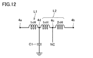
- FIG. 12 is a circuit diagram of a filter circuit including the coil component of the second connection according to the fourth embodiment.
- the coil component 1 according to the fourth embodiment further includes an electrode 4d provided on the fourth surface of the side surface facing the third surface and electrically connected to the coil L1 and the coil L2.
- One of the electrode 4c and the electrode 4d is connected to the ground via the capacitor C1.
- the inductance of the coil L1 with respect to the coil L2 can be changed depending on whether the capacitor C1 is connected to the electrode 4c or the capacitor C1 is connected to the electrode 4d.
- a connection (second connection) in which the inductance of the coil L1 is smaller than that of the coil L2 it is possible to improve the rise of the charge supplied from the capacitor C1 connected to the electrode 4c.
- the filter circuit 100 includes the coil component 1 described above, and a capacitor C1 connected to the electrode 4d between the coil L1 and the coil L2 of the coil component 1. As a result, the filter circuit 100 can improve the rise of the electric charge supplied from the capacitor C1 to the circuit component 200 connected via the coil L1.
- FIG. 13 is a cross-sectional view of a coil component according to a modified example. As shown in FIG. 13, the spacing in the stacking direction of the first wiring pattern 10 constituting the coil L1 is wider than the spacing in the stacking direction of the second wiring pattern 20 constituting the coil L2.
- the coil L1 can have a smaller inductance and resistance value than the coil L2 by widening the interval in the stacking direction of the wiring pattern as compared with the coil L2. Therefore, when the circuit component 200 is connected to the coil L1 shown in FIG. 13, the rise of the electric charge supplied from the capacitor C1 can be improved.
- the inductance and resistance value of the coil L1 are smaller than those of the coil L2.
- the coil L2 laminated on the upper layer of the coil L1 may have a smaller inductance and resistance value than the coil L1. That is, the coil L2 may be the first coil connected to the circuit component.
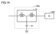
- FIG. 14 is a schematic diagram showing the configuration of an electronic device as a modified example.
- the electronic device shown in FIG. 14 includes a circuit component 200 mounted on a substrate (not shown) and a filter circuit 100a connecting one end to the circuit component 200.
- the circuit component 200 is an integrated circuit such as an IC, and uses the electric charge stored in the capacitor included in the filter circuit 100a when the power consumption temporarily increases.
- the filter circuit 100a has a coil component 1a and a capacitor C1, and the circuit component 200 is connected to the electrode 4b of the coil L2.
- the coil component 1a has a configuration in which the coil L2 is laminated on the upper layer of the coil L1, but the inductance and resistance value of the coil L2 are smaller than those of the coil L1. Therefore, as shown in FIG. 14, when the circuit component 200 is connected to the coil L2 of the coil component 1a, the rise of the electric charge supplied from the capacitor C1 can be improved.
- the coil L2 is used as the first coil.
- the coil component 1 described so far is composed of a laminated body 3 (ceramic prime field) of a plurality of ceramic layers laminated, any dielectric multi-layer structure may be used.
Landscapes
- Engineering & Computer Science (AREA)
- Power Engineering (AREA)
- Microelectronics & Electronic Packaging (AREA)
- Coils Or Transformers For Communication (AREA)
- Filters And Equalizers (AREA)
Priority Applications (4)
| Application Number | Priority Date | Filing Date | Title |
|---|---|---|---|
| JP2022505631A JP7107463B1 (ja) | 2020-10-01 | 2021-09-14 | 電子機器 |
| CN202190000600.1U CN219611741U (zh) | 2020-10-01 | 2021-09-14 | 线圈部件、包括该线圈部件的滤波器电路以及电子设备 |
| JP2022106934A JP2022130663A (ja) | 2020-10-01 | 2022-07-01 | コイル部品、これを含むフィルタ回路 |
| US18/109,896 US12355416B2 (en) | 2020-10-01 | 2023-02-15 | Coil component, filter circuit including the coil component, and electronic device |
Applications Claiming Priority (2)
| Application Number | Priority Date | Filing Date | Title |
|---|---|---|---|
| JP2020167205 | 2020-10-01 | ||
| JP2020-167205 | 2020-10-01 |
Related Child Applications (1)
| Application Number | Title | Priority Date | Filing Date |
|---|---|---|---|
| US18/109,896 Continuation US12355416B2 (en) | 2020-10-01 | 2023-02-15 | Coil component, filter circuit including the coil component, and electronic device |
Publications (1)
| Publication Number | Publication Date |
|---|---|
| WO2022070888A1 true WO2022070888A1 (ja) | 2022-04-07 |
Family
ID=80951431
Family Applications (1)
| Application Number | Title | Priority Date | Filing Date |
|---|---|---|---|
| PCT/JP2021/033751 Ceased WO2022070888A1 (ja) | 2020-10-01 | 2021-09-14 | コイル部品、これを含むフィルタ回路、および電子機器 |
Country Status (4)
| Country | Link |
|---|---|
| US (1) | US12355416B2 (https=) |
| JP (2) | JP7107463B1 (https=) |
| CN (1) | CN219611741U (https=) |
| WO (1) | WO2022070888A1 (https=) |
Cited By (6)
| Publication number | Priority date | Publication date | Assignee | Title |
|---|---|---|---|---|
| JPWO2023233966A1 (https=) * | 2022-06-01 | 2023-12-07 | ||
| WO2024154391A1 (ja) * | 2023-01-19 | 2024-07-25 | 株式会社村田製作所 | コイル部品、およびフィルタ回路 |
| WO2024154388A1 (ja) * | 2023-01-19 | 2024-07-25 | 株式会社村田製作所 | コイル部品、およびフィルタ回路 |
| WO2025062805A1 (ja) * | 2023-09-22 | 2025-03-27 | 株式会社村田製作所 | コイル部品、およびフィルタ回路 |
| WO2025083974A1 (ja) * | 2023-10-18 | 2025-04-24 | 株式会社村田製作所 | コイル部品、およびフィルタ回路 |
| WO2025210989A1 (ja) * | 2024-04-01 | 2025-10-09 | 株式会社村田製作所 | コイル部品、これを含む電子機器 |
Families Citing this family (1)
| Publication number | Priority date | Publication date | Assignee | Title |
|---|---|---|---|---|
| WO2024154387A1 (ja) * | 2023-01-19 | 2024-07-25 | 株式会社村田製作所 | コイル部品、これを含むフィルタ回路 |
Citations (4)
| Publication number | Priority date | Publication date | Assignee | Title |
|---|---|---|---|---|
| WO2016170708A1 (ja) * | 2015-04-20 | 2016-10-27 | 株式会社村田製作所 | 回路基板およびこれを用いたフィルタ回路 |
| WO2017199749A1 (ja) * | 2016-05-17 | 2017-11-23 | 株式会社村田製作所 | 積層型lcフィルタ |
| WO2018235527A1 (ja) * | 2017-06-19 | 2018-12-27 | 株式会社村田製作所 | 積層型素子およびlcフィルタ |
| WO2019107081A1 (ja) * | 2017-11-30 | 2019-06-06 | 株式会社村田製作所 | フィルタ回路、フィルタ回路素子および合分波器 |
Family Cites Families (10)
| Publication number | Priority date | Publication date | Assignee | Title |
|---|---|---|---|---|
| JP2001160728A (ja) | 1999-09-21 | 2001-06-12 | Murata Mfg Co Ltd | Lcフィルタ |
| CN1161880C (zh) | 1999-09-21 | 2004-08-11 | 株式会社村田制作所 | 电感电容滤波器 |
| JP2006270532A (ja) * | 2005-03-24 | 2006-10-05 | Tdk Corp | 積層基板及びパワーアンプ |
| JP2009153106A (ja) * | 2007-11-29 | 2009-07-09 | Hitachi Metals Ltd | バンドパスフィルタ、高周波部品および通信装置 |
| US8269581B2 (en) | 2007-11-29 | 2012-09-18 | Hitachi Metals, Ltd. | Band-pass filter, high-frequency component, and communication apparatus |
| CN113114150B (zh) | 2015-12-24 | 2024-01-16 | 株式会社村田制作所 | 滤波器电路以及电容元件 |
| US10141908B2 (en) * | 2016-08-18 | 2018-11-27 | Qualcomm Incorporated | Multi-density MIM capacitor for improved passive on glass (POG) multiplexer performance |
| KR101843283B1 (ko) * | 2016-09-20 | 2018-03-28 | 삼성전기주식회사 | 코일 전자 부품 |
| CN109906553B (zh) * | 2016-11-07 | 2023-06-06 | 株式会社村田制作所 | 层叠型lc滤波器 |
| CN217588590U (zh) * | 2018-12-10 | 2022-10-14 | 株式会社村田制作所 | 线圈部件以及包含该线圈部件的滤波器电路 |
-
2021
- 2021-09-14 WO PCT/JP2021/033751 patent/WO2022070888A1/ja not_active Ceased
- 2021-09-14 JP JP2022505631A patent/JP7107463B1/ja active Active
- 2021-09-14 CN CN202190000600.1U patent/CN219611741U/zh active Active
-
2022
- 2022-07-01 JP JP2022106934A patent/JP2022130663A/ja active Pending
-
2023
- 2023-02-15 US US18/109,896 patent/US12355416B2/en active Active
Patent Citations (4)
| Publication number | Priority date | Publication date | Assignee | Title |
|---|---|---|---|---|
| WO2016170708A1 (ja) * | 2015-04-20 | 2016-10-27 | 株式会社村田製作所 | 回路基板およびこれを用いたフィルタ回路 |
| WO2017199749A1 (ja) * | 2016-05-17 | 2017-11-23 | 株式会社村田製作所 | 積層型lcフィルタ |
| WO2018235527A1 (ja) * | 2017-06-19 | 2018-12-27 | 株式会社村田製作所 | 積層型素子およびlcフィルタ |
| WO2019107081A1 (ja) * | 2017-11-30 | 2019-06-06 | 株式会社村田製作所 | フィルタ回路、フィルタ回路素子および合分波器 |
Cited By (8)
| Publication number | Priority date | Publication date | Assignee | Title |
|---|---|---|---|---|
| JPWO2023233966A1 (https=) * | 2022-06-01 | 2023-12-07 | ||
| WO2023233966A1 (ja) * | 2022-06-01 | 2023-12-07 | 株式会社村田製作所 | コイル部品、およびこれを含むフィルタ回路 |
| JP7694825B2 (ja) | 2022-06-01 | 2025-06-18 | 株式会社村田製作所 | コイル部品、およびこれを含むフィルタ回路 |
| WO2024154391A1 (ja) * | 2023-01-19 | 2024-07-25 | 株式会社村田製作所 | コイル部品、およびフィルタ回路 |
| WO2024154388A1 (ja) * | 2023-01-19 | 2024-07-25 | 株式会社村田製作所 | コイル部品、およびフィルタ回路 |
| WO2025062805A1 (ja) * | 2023-09-22 | 2025-03-27 | 株式会社村田製作所 | コイル部品、およびフィルタ回路 |
| WO2025083974A1 (ja) * | 2023-10-18 | 2025-04-24 | 株式会社村田製作所 | コイル部品、およびフィルタ回路 |
| WO2025210989A1 (ja) * | 2024-04-01 | 2025-10-09 | 株式会社村田製作所 | コイル部品、これを含む電子機器 |
Also Published As
| Publication number | Publication date |
|---|---|
| JP7107463B1 (ja) | 2022-07-27 |
| CN219611741U (zh) | 2023-08-29 |
| JPWO2022070888A1 (https=) | 2022-04-07 |
| US20230198490A1 (en) | 2023-06-22 |
| JP2022130663A (ja) | 2022-09-06 |
| US12355416B2 (en) | 2025-07-08 |
Similar Documents
| Publication | Publication Date | Title |
|---|---|---|
| WO2022070888A1 (ja) | コイル部品、これを含むフィルタ回路、および電子機器 | |
| CN216162684U (zh) | 线圈部件及包含该线圈部件的滤波器电路 | |
| JP6733856B1 (ja) | コイル部品および、これを含むフィルタ回路 | |
| JP7318815B2 (ja) | フィルタ回路および、これを含む電源装置 | |
| US11264162B2 (en) | Coil component and filter circuit including the coil component | |
| US10284164B2 (en) | Circuit substrate, filter circuit, and capacitance element | |
| JP6981584B2 (ja) | 多層基板、回路装置、およびフィルタ回路基板 | |
| CN217216514U (zh) | 电路装置以及滤波器电路 | |
| WO2023090181A1 (ja) | 回路装置 | |
| CN222980246U (zh) | 线圈部件和包含该线圈部件的滤波电路 | |
| WO2022137678A1 (ja) | コイル部品および、これを含むフィルタ回路 |
Legal Events
| Date | Code | Title | Description |
|---|---|---|---|
| ENP | Entry into the national phase |
Ref document number: 2022505631 Country of ref document: JP Kind code of ref document: A |
|
| 121 | Ep: the epo has been informed by wipo that ep was designated in this application |
Ref document number: 21875190 Country of ref document: EP Kind code of ref document: A1 |
|
| WWE | Wipo information: entry into national phase |
Ref document number: 202190000600.1 Country of ref document: CN |
|
| NENP | Non-entry into the national phase |
Ref country code: DE |
|
| 122 | Ep: pct application non-entry in european phase |
Ref document number: 21875190 Country of ref document: EP Kind code of ref document: A1 |