WO2022059704A1 - Électrode ou câblage, paire d'électrodes et procédé de fabrication d'électrode ou de câblage - Google Patents
Électrode ou câblage, paire d'électrodes et procédé de fabrication d'électrode ou de câblage Download PDFInfo
- Publication number
- WO2022059704A1 WO2022059704A1 PCT/JP2021/033929 JP2021033929W WO2022059704A1 WO 2022059704 A1 WO2022059704 A1 WO 2022059704A1 JP 2021033929 W JP2021033929 W JP 2021033929W WO 2022059704 A1 WO2022059704 A1 WO 2022059704A1
- Authority
- WO
- WIPO (PCT)
- Prior art keywords
- electrode
- particles
- wiring
- metal
- atom
- Prior art date
Links
- 238000004519 manufacturing process Methods 0.000 title claims abstract description 25
- 238000000034 method Methods 0.000 title abstract description 19
- 239000002245 particle Substances 0.000 claims abstract description 57
- 229910052751 metal Inorganic materials 0.000 claims abstract description 49
- 239000002184 metal Substances 0.000 claims abstract description 49
- 239000000463 material Substances 0.000 claims abstract description 46
- 239000002923 metal particle Substances 0.000 claims abstract description 43
- 229910052799 carbon Inorganic materials 0.000 claims abstract description 27
- 229910052757 nitrogen Inorganic materials 0.000 claims abstract description 18
- 125000004432 carbon atom Chemical group C* 0.000 claims abstract description 14
- 238000012986 modification Methods 0.000 claims abstract description 14
- 230000004048 modification Effects 0.000 claims abstract description 14
- 125000004433 nitrogen atom Chemical group N* 0.000 claims abstract description 13
- 125000001309 chloro group Chemical group Cl* 0.000 claims abstract description 12
- 125000001153 fluoro group Chemical group F* 0.000 claims abstract description 12
- 125000004435 hydrogen atom Chemical group [H]* 0.000 claims abstract description 12
- 125000002887 hydroxy group Chemical group [H]O* 0.000 claims abstract description 12
- 125000004430 oxygen atom Chemical group O* 0.000 claims abstract description 12
- 229910052801 chlorine Inorganic materials 0.000 claims abstract description 11
- 229910052731 fluorine Inorganic materials 0.000 claims abstract description 11
- 239000000203 mixture Substances 0.000 claims description 46
- 229920005989 resin Polymers 0.000 claims description 19
- 239000011347 resin Substances 0.000 claims description 19
- 229910052719 titanium Inorganic materials 0.000 claims description 15
- 238000004898 kneading Methods 0.000 claims description 11
- 238000002156 mixing Methods 0.000 claims description 11
- 238000001035 drying Methods 0.000 claims description 10
- 229910052709 silver Inorganic materials 0.000 claims description 10
- 229910052720 vanadium Inorganic materials 0.000 claims description 9
- 229910052750 molybdenum Inorganic materials 0.000 claims description 8
- 229910052804 chromium Inorganic materials 0.000 claims description 7
- 238000010304 firing Methods 0.000 claims description 7
- 229910052758 niobium Inorganic materials 0.000 claims description 7
- 229910052718 tin Inorganic materials 0.000 claims description 7
- 229910052802 copper Inorganic materials 0.000 claims description 6
- 229910052737 gold Inorganic materials 0.000 claims description 6
- 238000000465 moulding Methods 0.000 claims description 6
- 229910052759 nickel Inorganic materials 0.000 claims description 6
- 229910052697 platinum Inorganic materials 0.000 claims description 6
- 229910052725 zinc Inorganic materials 0.000 claims description 6
- 229910052726 zirconium Inorganic materials 0.000 claims description 6
- 239000002131 composite material Substances 0.000 claims description 5
- 229910052735 hafnium Inorganic materials 0.000 claims description 5
- 229910052715 tantalum Inorganic materials 0.000 claims description 4
- 229910052748 manganese Inorganic materials 0.000 claims description 3
- 239000010410 layer Substances 0.000 description 66
- 238000013508 migration Methods 0.000 description 43
- 230000005012 migration Effects 0.000 description 43
- 150000002500 ions Chemical class 0.000 description 40
- 239000010936 titanium Substances 0.000 description 40
- 239000012298 atmosphere Substances 0.000 description 21
- 238000011156 evaluation Methods 0.000 description 18
- 125000004429 atom Chemical group 0.000 description 16
- 239000000843 powder Substances 0.000 description 14
- 239000007788 liquid Substances 0.000 description 13
- 239000000047 product Substances 0.000 description 12
- 230000000052 comparative effect Effects 0.000 description 10
- -1 hydrotalcite compound Chemical class 0.000 description 9
- 230000000694 effects Effects 0.000 description 8
- 239000000758 substrate Substances 0.000 description 8
- 239000004927 clay Substances 0.000 description 7
- 229910021645 metal ion Inorganic materials 0.000 description 7
- 238000002360 preparation method Methods 0.000 description 6
- 239000006185 dispersion Substances 0.000 description 5
- 238000005530 etching Methods 0.000 description 5
- 239000002356 single layer Substances 0.000 description 5
- 230000001629 suppression Effects 0.000 description 5
- VEXZGXHMUGYJMC-UHFFFAOYSA-N Hydrochloric acid Chemical compound Cl VEXZGXHMUGYJMC-UHFFFAOYSA-N 0.000 description 4
- 238000000576 coating method Methods 0.000 description 4
- 239000013078 crystal Substances 0.000 description 4
- 210000001787 dendrite Anatomy 0.000 description 4
- 239000012530 fluid Substances 0.000 description 4
- PQXKHYXIUOZZFA-UHFFFAOYSA-M lithium fluoride Chemical compound [Li+].[F-] PQXKHYXIUOZZFA-UHFFFAOYSA-M 0.000 description 4
- 239000004332 silver Substances 0.000 description 4
- 150000001449 anionic compounds Chemical class 0.000 description 3
- 239000011230 binding agent Substances 0.000 description 3
- 229910001412 inorganic anion Inorganic materials 0.000 description 3
- 230000001590 oxidative effect Effects 0.000 description 3
- 239000000126 substance Substances 0.000 description 3
- XLYOFNOQVPJJNP-UHFFFAOYSA-N water Substances O XLYOFNOQVPJJNP-UHFFFAOYSA-N 0.000 description 3
- VXQBJTKSVGFQOL-UHFFFAOYSA-N 2-(2-butoxyethoxy)ethyl acetate Chemical compound CCCCOCCOCCOC(C)=O VXQBJTKSVGFQOL-UHFFFAOYSA-N 0.000 description 2
- 239000004925 Acrylic resin Substances 0.000 description 2
- 229920000178 Acrylic resin Polymers 0.000 description 2
- 241000270728 Alligator Species 0.000 description 2
- KRHYYFGTRYWZRS-UHFFFAOYSA-N Fluorane Chemical compound F KRHYYFGTRYWZRS-UHFFFAOYSA-N 0.000 description 2
- BQCADISMDOOEFD-UHFFFAOYSA-N Silver Chemical compound [Ag] BQCADISMDOOEFD-UHFFFAOYSA-N 0.000 description 2
- MCMNRKCIXSYSNV-UHFFFAOYSA-N Zirconium dioxide Chemical compound O=[Zr]=O MCMNRKCIXSYSNV-UHFFFAOYSA-N 0.000 description 2
- 230000009471 action Effects 0.000 description 2
- 239000011248 coating agent Substances 0.000 description 2
- 150000001875 compounds Chemical class 0.000 description 2
- 239000004020 conductor Substances 0.000 description 2
- 230000007547 defect Effects 0.000 description 2
- 238000003618 dip coating Methods 0.000 description 2
- 229920001971 elastomer Polymers 0.000 description 2
- 230000005684 electric field Effects 0.000 description 2
- 239000003822 epoxy resin Substances 0.000 description 2
- 238000010438 heat treatment Methods 0.000 description 2
- 239000011229 interlayer Substances 0.000 description 2
- 238000007561 laser diffraction method Methods 0.000 description 2
- 238000005259 measurement Methods 0.000 description 2
- 230000007246 mechanism Effects 0.000 description 2
- 150000002894 organic compounds Chemical class 0.000 description 2
- 229920000647 polyepoxide Polymers 0.000 description 2
- 239000002244 precipitate Substances 0.000 description 2
- 238000007639 printing Methods 0.000 description 2
- 238000000790 scattering method Methods 0.000 description 2
- 238000007650 screen-printing Methods 0.000 description 2
- 239000013049 sediment Substances 0.000 description 2
- 238000000926 separation method Methods 0.000 description 2
- NDVLTYZPCACLMA-UHFFFAOYSA-N silver oxide Chemical compound [O-2].[Ag+].[Ag+] NDVLTYZPCACLMA-UHFFFAOYSA-N 0.000 description 2
- 239000000243 solution Substances 0.000 description 2
- 238000004528 spin coating Methods 0.000 description 2
- 238000005507 spraying Methods 0.000 description 2
- 239000006228 supernatant Substances 0.000 description 2
- 210000004243 sweat Anatomy 0.000 description 2
- 238000012360 testing method Methods 0.000 description 2
- 229920001187 thermosetting polymer Polymers 0.000 description 2
- 229910052721 tungsten Inorganic materials 0.000 description 2
- 238000005406 washing Methods 0.000 description 2
- 229920002799 BoPET Polymers 0.000 description 1
- 239000004640 Melamine resin Substances 0.000 description 1
- 229920000877 Melamine resin Polymers 0.000 description 1
- 239000004952 Polyamide Substances 0.000 description 1
- 239000004721 Polyphenylene oxide Substances 0.000 description 1
- RTAQQCXQSZGOHL-UHFFFAOYSA-N Titanium Chemical compound [Ti] RTAQQCXQSZGOHL-UHFFFAOYSA-N 0.000 description 1
- 238000002441 X-ray diffraction Methods 0.000 description 1
- 229910052782 aluminium Inorganic materials 0.000 description 1
- 238000005349 anion exchange Methods 0.000 description 1
- 239000007864 aqueous solution Substances 0.000 description 1
- 229910052785 arsenic Inorganic materials 0.000 description 1
- 230000005540 biological transmission Effects 0.000 description 1
- 229910052793 cadmium Inorganic materials 0.000 description 1
- 230000008859 change Effects 0.000 description 1
- 239000003638 chemical reducing agent Substances 0.000 description 1
- 229920006026 co-polymeric resin Polymers 0.000 description 1
- 238000010908 decantation Methods 0.000 description 1
- 230000007423 decrease Effects 0.000 description 1
- 230000032798 delamination Effects 0.000 description 1
- 238000010586 diagram Methods 0.000 description 1
- 238000000605 extraction Methods 0.000 description 1
- 238000004108 freeze drying Methods 0.000 description 1
- 229910052733 gallium Inorganic materials 0.000 description 1
- 229910052732 germanium Inorganic materials 0.000 description 1
- 229960001545 hydrotalcite Drugs 0.000 description 1
- 229910001701 hydrotalcite Inorganic materials 0.000 description 1
- 229910052738 indium Inorganic materials 0.000 description 1
- 150000002484 inorganic compounds Chemical class 0.000 description 1
- 229910010272 inorganic material Inorganic materials 0.000 description 1
- 229910052745 lead Inorganic materials 0.000 description 1
- 229910044991 metal oxide Inorganic materials 0.000 description 1
- 150000004706 metal oxides Chemical class 0.000 description 1
- 239000011812 mixed powder Substances 0.000 description 1
- 239000011259 mixed solution Substances 0.000 description 1
- 239000004570 mortar (masonry) Substances 0.000 description 1
- 239000002135 nanosheet Substances 0.000 description 1
- 239000003960 organic solvent Substances 0.000 description 1
- 239000007800 oxidant agent Substances 0.000 description 1
- 230000002093 peripheral effect Effects 0.000 description 1
- 239000005011 phenolic resin Substances 0.000 description 1
- 229910052698 phosphorus Inorganic materials 0.000 description 1
- 229920002647 polyamide Polymers 0.000 description 1
- 229920000728 polyester Polymers 0.000 description 1
- 229920000570 polyether Polymers 0.000 description 1
- 229920000139 polyethylene terephthalate Polymers 0.000 description 1
- 239000005020 polyethylene terephthalate Substances 0.000 description 1
- 229920000642 polymer Polymers 0.000 description 1
- 229920001343 polytetrafluoroethylene Polymers 0.000 description 1
- 239000004810 polytetrafluoroethylene Substances 0.000 description 1
- 229920002635 polyurethane Polymers 0.000 description 1
- 239000004814 polyurethane Substances 0.000 description 1
- 239000004800 polyvinyl chloride Substances 0.000 description 1
- 229920000915 polyvinyl chloride Polymers 0.000 description 1
- 238000001556 precipitation Methods 0.000 description 1
- 238000012545 processing Methods 0.000 description 1
- 230000027756 respiratory electron transport chain Effects 0.000 description 1
- 229910052706 scandium Inorganic materials 0.000 description 1
- 229910052710 silicon Inorganic materials 0.000 description 1
- 229910001923 silver oxide Inorganic materials 0.000 description 1
- 239000007787 solid Substances 0.000 description 1
- 239000002904 solvent Substances 0.000 description 1
- 238000000527 sonication Methods 0.000 description 1
- 238000003756 stirring Methods 0.000 description 1
- 229910052717 sulfur Inorganic materials 0.000 description 1
- 239000000725 suspension Substances 0.000 description 1
- 229910052716 thallium Inorganic materials 0.000 description 1
- 229920005992 thermoplastic resin Polymers 0.000 description 1
- 229910052723 transition metal Inorganic materials 0.000 description 1
- 150000003624 transition metals Chemical class 0.000 description 1
- GPPXJZIENCGNKB-UHFFFAOYSA-N vanadium Chemical compound [V]#[V] GPPXJZIENCGNKB-UHFFFAOYSA-N 0.000 description 1
- 239000002966 varnish Substances 0.000 description 1
- 125000000391 vinyl group Chemical group [H]C([*])=C([H])[H] 0.000 description 1
- 229920002554 vinyl polymer Polymers 0.000 description 1
- 239000011800 void material Substances 0.000 description 1
Images


Classifications
-
- H—ELECTRICITY
- H01—ELECTRIC ELEMENTS
- H01B—CABLES; CONDUCTORS; INSULATORS; SELECTION OF MATERIALS FOR THEIR CONDUCTIVE, INSULATING OR DIELECTRIC PROPERTIES
- H01B1/00—Conductors or conductive bodies characterised by the conductive materials; Selection of materials as conductors
- H01B1/20—Conductive material dispersed in non-conductive organic material
- H01B1/22—Conductive material dispersed in non-conductive organic material the conductive material comprising metals or alloys
-
- B—PERFORMING OPERATIONS; TRANSPORTING
- B22—CASTING; POWDER METALLURGY
- B22F—WORKING METALLIC POWDER; MANUFACTURE OF ARTICLES FROM METALLIC POWDER; MAKING METALLIC POWDER; APPARATUS OR DEVICES SPECIALLY ADAPTED FOR METALLIC POWDER
- B22F5/00—Manufacture of workpieces or articles from metallic powder characterised by the special shape of the product
-
- C—CHEMISTRY; METALLURGY
- C01—INORGANIC CHEMISTRY
- C01B—NON-METALLIC ELEMENTS; COMPOUNDS THEREOF; METALLOIDS OR COMPOUNDS THEREOF NOT COVERED BY SUBCLASS C01C
- C01B32/00—Carbon; Compounds thereof
- C01B32/90—Carbides
- C01B32/907—Oxycarbides; Sulfocarbides; Mixture of carbides
-
- C—CHEMISTRY; METALLURGY
- C22—METALLURGY; FERROUS OR NON-FERROUS ALLOYS; TREATMENT OF ALLOYS OR NON-FERROUS METALS
- C22C—ALLOYS
- C22C1/00—Making non-ferrous alloys
- C22C1/04—Making non-ferrous alloys by powder metallurgy
- C22C1/0408—Light metal alloys
- C22C1/0416—Aluminium-based alloys
-
- C—CHEMISTRY; METALLURGY
- C22—METALLURGY; FERROUS OR NON-FERROUS ALLOYS; TREATMENT OF ALLOYS OR NON-FERROUS METALS
- C22C—ALLOYS
- C22C1/00—Making non-ferrous alloys
- C22C1/04—Making non-ferrous alloys by powder metallurgy
- C22C1/045—Alloys based on refractory metals
- C22C1/0458—Alloys based on titanium, zirconium or hafnium
-
- C—CHEMISTRY; METALLURGY
- C22—METALLURGY; FERROUS OR NON-FERROUS ALLOYS; TREATMENT OF ALLOYS OR NON-FERROUS METALS
- C22C—ALLOYS
- C22C1/00—Making non-ferrous alloys
- C22C1/04—Making non-ferrous alloys by powder metallurgy
- C22C1/05—Mixtures of metal powder with non-metallic powder
-
- H—ELECTRICITY
- H01—ELECTRIC ELEMENTS
- H01B—CABLES; CONDUCTORS; INSULATORS; SELECTION OF MATERIALS FOR THEIR CONDUCTIVE, INSULATING OR DIELECTRIC PROPERTIES
- H01B1/00—Conductors or conductive bodies characterised by the conductive materials; Selection of materials as conductors
- H01B1/02—Conductors or conductive bodies characterised by the conductive materials; Selection of materials as conductors mainly consisting of metals or alloys
- H01B1/026—Alloys based on copper
-
- H—ELECTRICITY
- H01—ELECTRIC ELEMENTS
- H01B—CABLES; CONDUCTORS; INSULATORS; SELECTION OF MATERIALS FOR THEIR CONDUCTIVE, INSULATING OR DIELECTRIC PROPERTIES
- H01B1/00—Conductors or conductive bodies characterised by the conductive materials; Selection of materials as conductors
- H01B1/04—Conductors or conductive bodies characterised by the conductive materials; Selection of materials as conductors mainly consisting of carbon-silicon compounds, carbon or silicon
-
- H—ELECTRICITY
- H01—ELECTRIC ELEMENTS
- H01B—CABLES; CONDUCTORS; INSULATORS; SELECTION OF MATERIALS FOR THEIR CONDUCTIVE, INSULATING OR DIELECTRIC PROPERTIES
- H01B1/00—Conductors or conductive bodies characterised by the conductive materials; Selection of materials as conductors
- H01B1/06—Conductors or conductive bodies characterised by the conductive materials; Selection of materials as conductors mainly consisting of other non-metallic substances
-
- H—ELECTRICITY
- H01—ELECTRIC ELEMENTS
- H01B—CABLES; CONDUCTORS; INSULATORS; SELECTION OF MATERIALS FOR THEIR CONDUCTIVE, INSULATING OR DIELECTRIC PROPERTIES
- H01B13/00—Apparatus or processes specially adapted for manufacturing conductors or cables
-
- H—ELECTRICITY
- H05—ELECTRIC TECHNIQUES NOT OTHERWISE PROVIDED FOR
- H05K—PRINTED CIRCUITS; CASINGS OR CONSTRUCTIONAL DETAILS OF ELECTRIC APPARATUS; MANUFACTURE OF ASSEMBLAGES OF ELECTRICAL COMPONENTS
- H05K1/00—Printed circuits
- H05K1/02—Details
- H05K1/09—Use of materials for the conductive, e.g. metallic pattern
- H05K1/092—Dispersed materials, e.g. conductive pastes or inks
- H05K1/095—Dispersed materials, e.g. conductive pastes or inks for polymer thick films, i.e. having a permanent organic polymeric binder
-
- H—ELECTRICITY
- H05—ELECTRIC TECHNIQUES NOT OTHERWISE PROVIDED FOR
- H05K—PRINTED CIRCUITS; CASINGS OR CONSTRUCTIONAL DETAILS OF ELECTRIC APPARATUS; MANUFACTURE OF ASSEMBLAGES OF ELECTRICAL COMPONENTS
- H05K1/00—Printed circuits
- H05K1/02—Details
- H05K1/09—Use of materials for the conductive, e.g. metallic pattern
- H05K1/092—Dispersed materials, e.g. conductive pastes or inks
- H05K1/097—Inks comprising nanoparticles and specially adapted for being sintered at low temperature
-
- H—ELECTRICITY
- H05—ELECTRIC TECHNIQUES NOT OTHERWISE PROVIDED FOR
- H05K—PRINTED CIRCUITS; CASINGS OR CONSTRUCTIONAL DETAILS OF ELECTRIC APPARATUS; MANUFACTURE OF ASSEMBLAGES OF ELECTRICAL COMPONENTS
- H05K3/00—Apparatus or processes for manufacturing printed circuits
- H05K3/30—Assembling printed circuits with electric components, e.g. with resistor
- H05K3/32—Assembling printed circuits with electric components, e.g. with resistor electrically connecting electric components or wires to printed circuits
- H05K3/321—Assembling printed circuits with electric components, e.g. with resistor electrically connecting electric components or wires to printed circuits by conductive adhesives
-
- B—PERFORMING OPERATIONS; TRANSPORTING
- B22—CASTING; POWDER METALLURGY
- B22F—WORKING METALLIC POWDER; MANUFACTURE OF ARTICLES FROM METALLIC POWDER; MAKING METALLIC POWDER; APPARATUS OR DEVICES SPECIALLY ADAPTED FOR METALLIC POWDER
- B22F9/00—Making metallic powder or suspensions thereof
- B22F9/02—Making metallic powder or suspensions thereof using physical processes
- B22F9/04—Making metallic powder or suspensions thereof using physical processes starting from solid material, e.g. by crushing, grinding or milling
- B22F2009/043—Making metallic powder or suspensions thereof using physical processes starting from solid material, e.g. by crushing, grinding or milling by ball milling
-
- B—PERFORMING OPERATIONS; TRANSPORTING
- B22—CASTING; POWDER METALLURGY
- B22F—WORKING METALLIC POWDER; MANUFACTURE OF ARTICLES FROM METALLIC POWDER; MAKING METALLIC POWDER; APPARATUS OR DEVICES SPECIALLY ADAPTED FOR METALLIC POWDER
- B22F2999/00—Aspects linked to processes or compositions used in powder metallurgy
-
- H—ELECTRICITY
- H05—ELECTRIC TECHNIQUES NOT OTHERWISE PROVIDED FOR
- H05K—PRINTED CIRCUITS; CASINGS OR CONSTRUCTIONAL DETAILS OF ELECTRIC APPARATUS; MANUFACTURE OF ASSEMBLAGES OF ELECTRICAL COMPONENTS
- H05K2201/00—Indexing scheme relating to printed circuits covered by H05K1/00
- H05K2201/02—Fillers; Particles; Fibers; Reinforcement materials
- H05K2201/0203—Fillers and particles
- H05K2201/0206—Materials
- H05K2201/0209—Inorganic, non-metallic particles
-
- H—ELECTRICITY
- H05—ELECTRIC TECHNIQUES NOT OTHERWISE PROVIDED FOR
- H05K—PRINTED CIRCUITS; CASINGS OR CONSTRUCTIONAL DETAILS OF ELECTRIC APPARATUS; MANUFACTURE OF ASSEMBLAGES OF ELECTRICAL COMPONENTS
- H05K2201/00—Indexing scheme relating to printed circuits covered by H05K1/00
- H05K2201/02—Fillers; Particles; Fibers; Reinforcement materials
- H05K2201/0203—Fillers and particles
- H05K2201/0206—Materials
- H05K2201/0215—Metallic fillers
-
- H—ELECTRICITY
- H05—ELECTRIC TECHNIQUES NOT OTHERWISE PROVIDED FOR
- H05K—PRINTED CIRCUITS; CASINGS OR CONSTRUCTIONAL DETAILS OF ELECTRIC APPARATUS; MANUFACTURE OF ASSEMBLAGES OF ELECTRICAL COMPONENTS
- H05K2201/00—Indexing scheme relating to printed circuits covered by H05K1/00
- H05K2201/02—Fillers; Particles; Fibers; Reinforcement materials
- H05K2201/0203—Fillers and particles
- H05K2201/0242—Shape of an individual particle
- H05K2201/0245—Flakes, flat particles or lamellar particles
-
- Y—GENERAL TAGGING OF NEW TECHNOLOGICAL DEVELOPMENTS; GENERAL TAGGING OF CROSS-SECTIONAL TECHNOLOGIES SPANNING OVER SEVERAL SECTIONS OF THE IPC; TECHNICAL SUBJECTS COVERED BY FORMER USPC CROSS-REFERENCE ART COLLECTIONS [XRACs] AND DIGESTS
- Y10—TECHNICAL SUBJECTS COVERED BY FORMER USPC
- Y10T—TECHNICAL SUBJECTS COVERED BY FORMER US CLASSIFICATION
- Y10T428/00—Stock material or miscellaneous articles
- Y10T428/12—All metal or with adjacent metals
- Y10T428/12014—All metal or with adjacent metals having metal particles
- Y10T428/12028—Composite; i.e., plural, adjacent, spatially distinct metal components [e.g., layers, etc.]
- Y10T428/12063—Nonparticulate metal component
- Y10T428/12139—Nonmetal particles in particulate component
Definitions
- the present invention relates to an electrode or wiring, an electrode pair, and a method for manufacturing an electrode or wiring.
- Patent Document 1 discloses an inorganic anion exchanger and an epoxy resin composition for encapsulating electronic components using the inorganic anion exchanger.
- Patent Document 2 discloses that a triazine compound, which is an organic compound, is dissolved or uniformly dispersed in a predetermined polymer to prevent migration of electronic parts and the like.
- the electrodes or wirings that make up the electronic components are required to have high conductivity as well as suppression of ion migration.
- both the inorganic compound shown in Patent Document 1 and the organic compound shown in Patent Document 2 exhibit insulating properties, their conductivity decreases when they are blended in an electrode.
- the present invention has been made in view of the above circumstances, and an object thereof is to manufacture an electrode or wiring, an electrode pair, and an electrode or wiring in which ion migration is suppressed under high humidity and the conductivity is excellent. Is to provide.
- the layer has the following formula: M m X n (In the formula, M is at least one group 3, 4, 5, 6, 7 metal, and X is a carbon atom, a nitrogen atom or a combination thereof, n is 1 or more and 4 or less, m is greater than n and less than or equal to 5)
- the layer body represented by and the modification or termination T existing on the surface of the layer body (T is at least one selected from the group consisting of a hydroxyl group, a fluorine atom, a chlorine atom, an oxygen atom and a hydrogen atom).
- An electrode or wiring is provided, including.
- the layer has the following formula: M m X n (In the formula, M is at least one group 3, 4, 5, 6, 7 metal, and X is a carbon atom, a nitrogen atom or a combination thereof, n is 1 or more and 4 or less, m is greater than n and less than or equal to 5)
- the layer body represented by and the modification or termination T existing on the surface of the layer body (T is at least one selected from the group consisting of a hydroxyl group, a fluorine atom, a chlorine atom, an oxygen atom and a hydrogen atom).
- T is at least one selected from the group consisting of a hydroxyl group, a fluorine atom, a chlorine atom, an oxygen atom and a hydrogen atom).
- gist of the invention (A1) To prepare a mixture by kneading particles of a layered material containing one or more layers, metal particles, and a resin.
- the layer has the following formula: M m X n (In the formula, M is at least one group 3, 4, 5, 6, 7 metal, and X is a carbon atom, a nitrogen atom or a combination thereof, n is 1 or more and 4 or less, m is greater than n and less than or equal to 5)
- the layer body represented by and the modification or termination T existing on the surface of the layer body (T is at least one selected from the group consisting of a hydroxyl group, a fluorine atom, a chlorine atom, an oxygen atom and a hydrogen atom).
- Including and The mixing ratio of the particles of the layered material in the mixture is 0.1% by mass or more and 20% by mass or less with respect to the metal particles, and (b1) the mixture is dried to obtain an electrode or a wiring.
- a method of manufacturing an electrode or wiring including the above is provided.
- the layer has the following formula: M m X n (In the formula, M is at least one group 3, 4, 5, 6, 7 metal, and X is a carbon atom, a nitrogen atom or a combination thereof, n is 1 or more and 4 or less, m is greater than n and less than or equal to 5)
- the layer body represented by and the modification or termination T existing on the surface of the layer body (T is at least one selected from the group consisting of a hydroxyl group, a fluorine atom, a chlorine atom, an oxygen atom and a hydrogen atom).
- a method for manufacturing an electrode or wiring comprises molding the mixture and drying it to obtain a molded product, and (c) firing the molded product at a temperature at which it can be sintered.
- the electrode or wiring comprises particles of a predetermined layered material (also referred to herein as "MXene”) and metal particles or sintered metal, thereby comprising MXene and high.
- MXene a predetermined layered material
- An electrode or wiring in which ion migration is suppressed even under humidity and has excellent conductivity is provided.
- a mixture of predetermined layered material particles (MXene particles), metal particles, and a resin is kneaded to prepare a mixture of the layered material particles in the mixture.
- the electrode or wiring can be manufactured by setting the blending ratio to 0.1% by mass or more and 20% by mass or less with respect to the metal particles and drying the mixture.
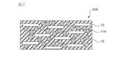
- FIG. 3 is a schematic schematic cross-sectional view showing an electrode or wiring according to another embodiment of the present invention.
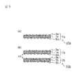
- FIG. 3 is a schematic schematic cross-sectional view showing MXene, which is a layered material that can be used as a conductive composite material in one embodiment of the present invention.
- MXene which is a layered material that can be used as a conductive composite material in one embodiment of the present invention.
- It is a schematic diagram explaining the generation mechanism of Ag ion migration.
- It is a photograph which shows the ion migration evaluation result of the comparative example.
- It is a photograph which shows the ion migration evaluation result of an Example.
- It is a photograph which shows the ion migration evaluation result of another comparative example.
- It is a photograph which shows the ion migration evaluation result of another Example.
- Electrode or wiring in the embodiment of the present invention contains particles of a predetermined layered material and metal particles or sintered metal, whereby ion migration is suppressed even under high humidity and excellent conductivity is obtained. Electrodes or wiring can be realized.
- the electrodes or wirings in the embodiment of the present invention will be described in detail, but the electrodes or wirings of the present invention are not limited to such embodiments.
- one electrode or wiring of the present embodiment includes an electrode or wiring 20A formed of a composite material containing particles 10 of a predetermined layered material, metal particles 11A, and resin 12. .. Further, with reference to FIG. 2, as another electrode or wiring of the present embodiment, an electrode or wiring 20B formed of a sintered body containing particles 10 of a predetermined layered material and sintered metal 11B can be mentioned. ..
- the composite material or sintered body is a material that easily forms electrodes or wiring.
- the particles of the predetermined layered material in the present embodiment are MXene (particles), and are defined as follows. Particles of a layered material containing one or more layers, the layer being of the following formula: M m X n (In the formula, M is at least one group 3, 4, 5, 6, 7 metal, so-called early transition metals such as Sc, Ti, Zr, Hf, V, Nb, Ta, Cr, Mo and It may contain at least one selected from the group consisting of Mn.
- X is a carbon atom, a nitrogen atom or a combination thereof, n is 1 or more and 4 or less, m is greater than n and less than or equal to 5)
- the layer body represented by may have a crystal lattice in which each X is located in an octahedral array of M) and the surface of the layer body (more specifically, facing each other of the layer body).
- a layered material containing a modification or termination T (T is at least one selected from the group consisting of a hydroxyl group, a fluorine atom, a chlorine atom, an oxygen atom and a hydrogen atom) present on at least one of the two surfaces thereof.
- T is at least one selected from the group consisting of a hydroxyl group, a fluorine atom, a chlorine atom, an oxygen atom and a hydrogen atom
- M is preferably at least one selected from the group consisting of Ti, Zr, Hf, V, Nb, Ta, Cr, Mo and Mn, preferably from Ti, V, Cr and Mo. More preferably, it is at least one selected from the group.
- Ti and X are carbon atoms, or carbon atoms and nitrogen atoms.
- the layer body at least one selected from the group consisting of Ti 3 C 2 , Ti 3 CN, and Ti 2 C is more preferable, and Ti 3 C 2 is particularly preferable. If MXene having the layer body is used, high conductivity can be ensured.
- Such MXene can be synthesized by selectively etching (removing and optionally layering) A atoms (and optionally a portion of M atoms) from the MAX phase.
- the MAX phase is as follows: M m AX n (In the formula, M, X, n and m are as described above, A is at least one group 12th, 13th, 14th, 15th and 16th element, usually a group A element, representatively.
- Is a group IIIA and a group IVA and more particularly may include at least one selected from the group consisting of Al, Ga, In, Tl, Si, Ge, Sn, Pb, P, As, S and Cd.
- a layer composed of A atoms is located between two layers represented by and represented by Mm Xn (each X may have a crystal lattice located in an octahedral array of M ). It has a crystal structure.
- Mm Xn a layer of X atoms
- MM X n layer a layer of A atoms
- a atom layer is arranged as a layer next to the n + 1th layer of M atoms, but is not limited to this.
- the A atom layer (and possibly part of the M atom) is removed by selectively etching (removing and possibly layering) the A atom (and possibly part of the M atom) from the MAX phase.
- etching solution usually, but not limited to, an aqueous solution of fluoroacid is used
- the etching can be carried out using an etching solution containing F ⁇ , and may be, for example, a method using a mixed solution of lithium fluoride and hydrochloric acid, a method using hydrofluoric acid, or the like. Then, as appropriate, any appropriate post-treatment (eg, sonication, handshake, etc.) may facilitate the layer separation of MXene (delamination, separation of multi-layer MXene into single-layer MXene).
- any appropriate post-treatment eg, sonication, handshake, etc.
- M can be titanium or vanadium and X can be a carbon atom or a nitrogen atom.
- the MAX phase is Ti 3 AlC 2 and MXene is Ti 3 C 2 T x (in other words, M is Ti, X is C, n is 2, and m is 3). Is).
- MXene may contain a relatively small amount of residual A atom, for example, 10% by mass or less with respect to the original A atom.
- the residual amount of A atom can be preferably 8% by mass or less, more preferably 6% by mass or less. However, even if the residual amount of A atom exceeds 10% by mass, there may be no problem depending on the use and conditions of use of the paste (and the conductive film obtained thereby).
- the MXene (particles) 10 synthesized in this way is, as schematically shown in FIG. 3, a layered material containing one or more MXene layers 7a, 7b (as an example of the MXene (particles) 10 in FIG. 3 (A) shows one layer of MXene10a and FIG. 3B shows two layers of MXene10b, but is not limited to these examples). More specifically, the MXene layers 7a and 7b are formed on the surfaces of the layer bodies ( MmXn layer) 1a and 1b represented by MmXn and the layer bodies 1a and 1b (more specifically, in each layer).
- MXene layers 7a and 7b are also expressed as "MM X n T x ", and x is an arbitrary number.
- MXene10 even if the MXene layers are individually separated and exist in one layer (single-layer structure shown in FIG. 3A, so-called single-layer MXene10a), a plurality of MXene layers are separated from each other. It may be a laminated body (multilayer structure shown in FIG. 3B, so-called multi-layer MXene10b) or a mixture thereof.
- MXene 10 can be particles (also referred to as powder or flakes) as an aggregate composed of single layer MXene 10a and / or multilayer MXene 10b.
- the MXene 10 is preferably particles (which may also be referred to as nanosheets), most of which are composed of a single layer MXene 10a.
- two adjacent MXene layers for example, 7a and 7b do not necessarily have to be completely separated, and may be partially in contact with each other.
- each layer of MXene is, for example, 0.8 nm or more and 5 nm or less, particularly 0.8 nm or more and 3 nm or less (mainly).
- the maximum dimensions in a plane parallel to the layers (two-dimensional sheet surface) are, for example, 0.1 ⁇ m or more, 200 ⁇ m or less, and particularly 1 ⁇ m or more and 40 ⁇ m or less.
- the interlayer distance is, for example, 0.8 nm or more and 10 nm or less, particularly 0.
- the size is, for example, 0.1 ⁇ m or more and 200 ⁇ m or less, particularly 1 ⁇ m or more and 40 ⁇ m or less, and the maximum dimension in a plane (two-dimensional sheet surface) perpendicular to the stacking direction is, for example, 0.1 ⁇ m or more and 100 ⁇ m or less, particularly 1 ⁇ m or more. It is 20 ⁇ m or less.
- these dimensions are number average dimensions (for example, at least 40 number averages) or X-ray diffraction (for example, number averages based on scanning electron microscope (SEM), transmission electron microscope (TEM) photographs or interatomic force microscope (AFM) photographs). It is obtained as the distance in the real space calculated from the position on the reciprocal lattice space of the (002) plane measured by the XRD) method.
- the type of metal constituting the metal particles 11A or the sintered metal 11B is not particularly limited.
- the electrode or wiring of the present embodiment may contain one or more elements selected from the group consisting of Ag, Sn, Pt, Ni, Cu, Au and Zn as the metal particles 11A or the sintered metal 11B. These elements are elements that can cause ion migration. When these elements are contained, particularly when Ag is contained, the ion migration suppressing effect is sufficiently exhibited.
- the metal particles 11A or the sintered metal 11B are formed of one or more elements selected from the group consisting of Ag, Sn, Pt, Ni, Cu, Au and Zn, especially when they are formed of Ag. , The effect of suppressing ion migration is fully exhibited.
- the size of the metal particles 11A is not particularly limited, but it is preferable that the average particle size (D50) measured by, for example, a laser diffraction / scattering method is in the range of 0.1 ⁇ m or more and 100 ⁇ m or less.
- the content of the particles of the layered material containing the one or more layers is preferably 0.1% by mass or more and 20% by mass or less with respect to the metal particles or the sintered metal. It is preferable that the content of the particles of the layered material is 0.1% by mass or more with respect to the metal particles or the sintered metal because the ion migration suppressing effect is more exhibited.
- the content is more preferably 1% by mass or more, still more preferably 3% by mass or more.
- the content is preferably 20% by mass or less, more preferably 15% by mass or less, still more preferably 10% by mass. It is as follows.
- the resin 12 in the electrode or the wiring 20A is not limited, and may be a thermosetting resin or a thermoplastic resin.
- acrylic resin, fluororesin such as polytetrafluoroethylene, vinyl resin such as polyvinyl chloride, epoxy resin, polyurethane, melamine resin, phenol resin, polyester such as polyethylene terephthalate, polyamide, polyether and the like can be mentioned.
- the proportion of the resin in the composite material constituting the electrode or the wiring 20A is preferably more than 0% by mass, preferably 2% by mass or more, in order to exert a function as a binder, for example, and on the other hand, from the viewpoint of ensuring conductivity. It is preferably 25% by mass or less, and more preferably 12% by mass or less.
- Electrode examples include internal electrodes, external electrodes, pad electrodes, wiring-like electrodes, ground (reference potential) electrodes, shield patterns, etc. in electronic components and circuit boards that may cause the ion migration failure. Be done.
- Examples of the "wiring” include signal lines forming circuit patterns, coil patterns, interlayer connection conductors (via conductors), and the like.
- the distance between the electrodes is more than 0 mm, for example, 6 mm or less, and the distance between the wirings is more than 0 mm, for example, 1 mm, although it depends on the atmosphere such as humidity.
- Liquid may exist between these electrodes and wiring. That is, the electrodes and wiring may be present in the atmosphere in which a small amount of the liquid is present, in addition to being present in the liquid.
- the atmosphere in which a small amount of liquid is present includes, for example, the case where the humidity in the atmosphere is high and the case where sweat, which is a liquid, is present on the surface of human skin.
- the electrode or wiring of the present embodiment can more effectively suppress ion migration in the atmosphere where a small amount of liquid is present.
- Electrode pair The electrode pair according to the embodiment of the present invention uses the electrode according to the embodiment of the present invention as at least one of the anode and the cathode, whereby ion migration can be effectively suppressed even under high humidity and the conductivity is conductive. It is possible to realize a pair of electrodes having excellent properties.
- the electrode pair in the embodiment of the present invention is described in detail.
- the layer has the following formula: M m X n (In the formula, M is at least one group 3, 4, 5, 6, 7 metal, and X is a carbon atom, a nitrogen atom or a combination thereof, n is 1 or more and 4 or less, m is greater than n and less than or equal to 5)
- the layer body represented by and the modification or termination T existing on the surface of the layer body (T is at least one selected from the group consisting of a hydroxyl group, a fluorine atom, a chlorine atom, an oxygen atom and a hydrogen atom). And include.
- At least one of the anode and the cathode may contain one or more elements selected from the group consisting of Ag, Sn, Pt, Ni, Cu, Au and Zn. These elements are elements that can cause ion migration. When these elements are contained, particularly when Ag is contained, the ion migration suppressing effect is sufficiently exhibited. When at least one of the anode and cathode is formed of one or more elements selected from the group consisting of Ag, Sn, Pt, Ni, Cu, Au and Zn, especially when formed of Ag. The effect of suppressing ion migration is fully exhibited.
- the metal particles or sintered metal contained together are not particularly limited. Therefore, the metal particles or sintered metal that can be contained in the anode and the cathode may be the same or different.
- Ag ion migration is considered to occur as schematically shown in FIG. That is, as shown in FIG. 4, Ag + , which is a metal ion, elutes from the anode 31, and as shown in FIG. 4, Ag + moves between the electrodes from the anode (positive electrode) 31 to the cathode (negative electrode) 33. Arrow 35 indicates the direction of the electric field. Then, as shown in C in FIG. 4, the metal ion Ag + arrives at the cathode 33 and precipitates as the metal Ag 37. At the time of precipitation, as shown in D in FIG. 4, it is easy to precipitate at the tip of the branch due to the shielding effect. Further, it is considered that when the crystal grows like a branch as shown in E in FIG. 4 and the branch grows while the electron is supplied from the cathode, it can be precipitated from the middle of the branch as shown in F in FIG.
- the metal ion that causes ion migration is suppressed by MXene from the extraction of electrons by the anode (positive electrode) and the change to the metal ion. Does not occur and ion migration is suppressed. It is considered that this is because the electrons of MXene are extracted instead of the metal, that is, MXene functions as a reducing agent.
- the metal at the cathode 33 (metal Ag37 in FIG. 4). ) Does not precipitate, and ion migration is suppressed. It is believed that this is because MXene receives electrons instead of metal ions, that is, it functions as an oxidant.
- the reason why ion migration is suppressed by the electrode pair in this embodiment is not limited to these, and other mechanisms such as not moving metal ions from the anode to the cathode can be considered.
- MXene which is a two-dimensional layered compound, has a feature of high conductivity and also has a redox action (electron transfer). It is considered that this redox action is effective in suppressing ion migration.
- the MXene is contained in at least one of the electrodes constituting the anode and the cathode of the electrode pair having the anode and the cathode.
- the distance between the anode and the cathode is, for example, as an embodiment in which the ion migration can occur, although it depends on the atmosphere such as humidity, it may be more than 0 ⁇ m and, for example, 6 mm or less.
- These anodes and cathodes may be present in the liquid or in the atmosphere in which a small amount of the liquid is present.
- the atmosphere in which a small amount of liquid is present includes, for example, the case where the humidity in the atmosphere is high and the case where sweat, which is a liquid, is present on the surface of human skin.
- the electrode or wiring of the present embodiment can more effectively suppress ion migration in the atmosphere where a small amount of liquid is present.
- the manufacturing method (first manufacturing method) of one electrode or wiring of this embodiment is (A1) A mixture is prepared by kneading predetermined layered material particles, metal particles, and a resin, and the mixing ratio of the layered material particles in the mixture is relative to the metal particles. Includes being 0.1% by weight or more and 20% by weight or less, and (b1) drying the mixture to obtain electrodes or wiring.
- the other electrode or wiring manufacturing method (second manufacturing method) of the present embodiment is (A2) A mixture containing particles of a predetermined layered material and metal particles is kneaded to prepare a mixture, and the mixing ratio of the particles of the layered material in the mixture is the metal particles. On the other hand, it should be 0.1% by mass or more and 20% by mass or less.
- (B2) includes molding and drying the mixture to obtain a molded product, and (c) firing the molded product at a sinterable temperature.
- the particles described in the first embodiment are used as particles of a predetermined layered material, that is, particles of a layered material containing one or more layers. Further, as the metal particles and the resin, the materials described in the first embodiment can be used. As the metal particles and the resin, a metal paste in which these are mixed in advance can be used.
- the mixing ratio of the particles of the layered material in the mixture is 0.1% by mass or more and 20% by mass or less with respect to the metal particles.
- the reason for setting the upper and lower limit values and the preferable upper and lower limit values are as described in the first embodiment.
- the kneading method is not particularly limited, and examples thereof include stirring with a centrifugal stirrer, kneading using a three-roll mill, and dispersion treatment. If the fluidity is reduced in the kneading, an organic solvent that can be removed in the drying step of the subsequent step, for example, diethylene glycol monobutyl ether acetate used in the examples may be added.
- the mixture is dried to obtain electrodes or wiring.
- the mixture can be molded into a molded product in the shape of an electrode or a wiring before drying, but the molding method is not particularly limited.
- the mixture may be applied to an object to be coated such as a substrate.
- the coating method is not limited, for example, a method of spray coating using a nozzle such as a 1-fluid nozzle, a 2-fluid nozzle, or an airbrush, a table coater, a comma coater, a slit coat using a bar coater, screen printing, and a metal mask. Examples thereof include methods such as printing, spin coating, dip coating, and application methods by dropping.
- a printed circuit board, a metal substrate, a resin substrate, a laminated electronic component, a metal pin, a metal wire, or the like may be appropriately adopted depending on the intended use.
- drying conditions depend on the shape and size of the molded mixture, but for example, it may be carried out in the range of 60 ° C. or higher and 200 ° C. or lower for 10 minutes or longer and 120 minutes or shorter.
- the above coating and drying may be repeated a plurality of times as necessary until a film having a desired thickness is obtained.
- the particles described in the first embodiment are used as particles of a predetermined layered material, that is, particles of a layered material containing one or more layers.
- the metal particles the material described in the first embodiment can be used.
- metal particles for example, metal particles having an average particle size (D50) of 1 nm or more and 200 ⁇ m or less measured by a laser diffraction / scattering method can be used.
- the mixture may contain a binder that can be removed by firing in a subsequent step for easy kneading.
- the mixing ratio of the particles of the layered material in the mixture is 0.1% by mass or more and 20% by mass or less with respect to the metal particles.
- the reason for setting the upper and lower limit values of the blending ratio and the preferable upper and lower limit values are as described in the first embodiment.
- the kneading method is not particularly limited, and examples thereof include a method of mixing and dispersing using a three-roll mill.
- the mixture is molded and dried to obtain a molded product.
- the molding method is not particularly limited, and molding may be performed by applying the mixture to an object to be coated, for example, a substrate.
- the coating method is not limited, for example, a method of spray coating using a nozzle such as a 1-fluid nozzle, a 2-fluid nozzle, or an airbrush, a table coater, a comma coater, a slit coat using a bar coater, screen printing, and a metal mask. Examples thereof include methods such as printing, spin coating, dip coating, and application methods by dropping.
- a printed circuit board, a metal substrate, a resin substrate, a laminated electronic component, a metal pin, a metal wire, or the like may be appropriately adopted depending on the intended use.
- the drying conditions depend on the shape and size of the molded product, but for example, it may be performed for 10 minutes or more and 120 minutes or less in the range of 60 ° C. or higher and 200 ° C. or lower.
- the molded product is fired at a temperature at which it can be sintered.
- the temperature at which sinterability can be performed may be determined, for example, in the range of approximately 150 ° C. or higher and 800 ° C. or lower, depending on the metal type. Further, the firing time may be determined according to the shape and size of the molded product.
- the atmosphere at the time of firing is not particularly limited. For the purpose of removing the binder and the like, the atmosphere at the time of firing can be appropriately adjusted to an inert atmosphere, an oxidizing atmosphere, and a reducing atmosphere.
- the manufacturing method of the electrode or wiring, the electrode pair, and the electrode or wiring in the embodiment of the present invention has been described in detail above, various modifications are possible. It should be noted that the electrodes or wirings of the present invention may be manufactured by a method different from the manufacturing method in the above-described embodiment.
- Example 1 -Preparation of MAX particles
- TiC powder, Ti powder and Al powder (all manufactured by High Purity Chemical Laboratory Co., Ltd.) were placed in a ball mill containing zirconia balls at a molar ratio of 2: 1: 1 and mixed for 24 hours. ..
- the obtained mixed powder was calcined at 1350 ° C. for 2 hours in an Ar atmosphere.
- the sintered body (block-shaped MAX phase) thus obtained was pulverized with an end mill to a maximum size of 40 ⁇ m or less.
- Ti 3 AlC 2 particles were obtained as MAX particles.
- Preparation of MXene clay and MXene powder Weigh 1 g of Ti 3 AlC 2 particles (powder) prepared by the above method, add 1 g of LiF to 10 mL of 9 mol / L hydrochloric acid, and stirrer at 35 ° C. for 24 hours. The mixture was stirred to obtain a solid-liquid mixture (suspension) containing a solid component derived from Ti 3 AlC 2 powder. To this, the operation of washing with pure water and separating and removing the supernatant liquid by decantation using a centrifuge (the remaining sediment excluding the supernatant is subjected to washing again) was repeated about 10 times, and clay was used as the sediment. A state substance (clay) was obtained. As a result, Ti 3 C 2 T x -aqueous dispersion clay was obtained as MXene clay. The aqueous dispersion clay was freeze-dried and pulverized using an IKA mill to obtain MXene powder.
- the MXene-blended Ag paste was dispersed using a three-roll machine.
- the rotation speed of the roll is 230 rpm, and the dispersion condition is that the rolls having a gap of 50 ⁇ m are passed twice, then the rolls having a gap of 20 ⁇ m are passed twice, and finally the rolls having a gap of 10 ⁇ m are passed twice.
- a paste of the mixture was obtained.
- the paste of the mixture was hand-painted on two substrates, respectively, to obtain a molded product of a pair of counter electrodes of an anode and a cathode with an interval of 1 mm.
- the molded product was dried at 140 ° C. for 30 minutes to obtain a pair of counter electrodes of the anode and the cathode as a sample for ion migration evaluation.
- a total of two samples for ion migration evaluation prepared by the same manufacturing method were prepared.
- the paste of the mixture containing MXene is printed on both the anode and the cathode, but the same effect can be obtained even when the paste of the mixture containing MXene is printed on one of the anode and the cathode.
- the resistance value of the electrode of the example formed by using the mixture containing Ag paste and MXene is the same as the resistance value of the electrode of the comparative example formed only by Ag paste, and in the case of Ag only. Maintained the same conductivity as.
- FIG. 5 is a photograph in the case of only Ag paste (without MXene, comparative example)
- FIG. 6 is a photograph in the case of Ag paste + MXene.
- FIG. 5 in the case of only Ag paste (without MXene), silver dendrites were generated on the cathode (negative electrode), and ion migration occurred.
- Example 2 MXene powder, Ag powder (size: 1 ⁇ m), and acrylic resin obtained by freeze-drying Ti 3 C 2 T x -aqueous dispersion clay in the same manner as in Example 1 and crushing it using an IKA mill.
- the varnishes were prepared in proportions of 1.9% by mass, 55.7% by mass and 42.4% by mass, respectively, and mixed in a mortar. After that, it was kneaded with a three-roll mill.
- the conditions for kneading with a three-roll mill were a gap between rolls of 10 ⁇ m and a peripheral speed of rolls of 230 rpm.
- the obtained paste was printed on a substrate via a metal mask matching the electrode shape, heated in an oven at 80 ° C.
- the electrode obtained in this embodiment also contains a predetermined MXene like the electrode according to the embodiment of Example 1, it is considered that the electrode has high conductivity and can prevent an ion migration failure.
- Example 3 Preparation of MAX particles and preparation of MXene powder The preparation of MAX particles and the preparation of MXene powder were carried out in the same manner as in Example 1.
- the MXene powder is added to Cu paste (manufactured by Nichiyu, trade name: CP-100D, containing 10% or more and 20% or less of a thermosetting resin as a resin) in an amount of 0.75% by mass (when dried) with respect to the metal particles. ) was compounded and stirred manually to obtain a paste of the mixture.
- the paste of the mixture was hand-painted on two PET films pre-annealed at 150 ° C. for 30 minutes, respectively, to form a pair of counter electrodes of the anode and cathode with 1 mm spacing. I got something.
- the molded product was dried at 150 ° C. for 30 minutes to obtain a pair of counter electrodes of the anode and the cathode as a sample for ion migration evaluation.
- Example 3 As a comparative example of Example 3, a pair of anode and cathode counter electrodes prepared in the same manner as above except that MXene was not added were obtained as a sample for ion migration evaluation.
- the resistance value of the counter electrode was measured with a tester. Specifically, the tester terminals were kept at regular intervals and brought into contact with each counter electrode to measure the resistance between the two points. Since the resistance value changes depending on the interval distance, the interval is kept constant in all measurements. The results of the electrode resistance values of the examples and the comparative examples were both 0.000 ⁇ .
- the resistance value of the electrode of the example formed by using the mixture containing Cu paste and MXene is the same as the resistance value of the electrode of the comparative example formed only by Cu paste.
- the same conductivity as in the case of Cu alone was maintained.
- FIG. 7 is a photograph in the case of Cu paste only (without MXene, comparative example), and FIG. 8 is a photograph in the case of Cu paste + MXene. As shown in FIG.
- the electrodes or wirings of the present invention may be utilized in any suitable application, and may be particularly preferably used, for example, for one or more of anodes and cathodes in electrode pairs of electronic components.
Abstract
L'invention concerne une électrode ou un câblage, une paire d'électrodes, ainsi qu'un procédé de fabrication de l'électrode ou du câblage. L'électrode ou le câblage comprend : des particules d'un matériau en couches comprenant une ou plusieurs couches ; et des particules métalliques ou un métal fritté. Les couches comprennent un corps de couche représenté par la formule MmXn (dans la formule, M représente au moins un métal appartenant au groupe 3, 4, 5, 6 ou 7, X est un atome de carbone, un atome d'azote ou une combinaison de ces derniers, n est un chiffre compris entre 1 et 4, et m est supérieur à n et n'est pas supérieur à 5), et une modification ou un terminal T (T étant au moins un élément choisi dans le groupe constitué par un groupe hydroxyle, un atome de fluor, un atome de chlore, un atome d'oxygène et un atome d'hydrogène) présent sur la surface du corps de couche.
Priority Applications (3)
| Application Number | Priority Date | Filing Date | Title |
|---|---|---|---|
| JP2022550582A JPWO2022059704A1 (fr) | 2020-09-17 | 2021-09-15 | |
| CN202180063284.7A CN116194236A (zh) | 2020-09-17 | 2021-09-15 | 电极或布线、电极对、以及电极或布线的制造方法 |
| US18/182,794 US20230223165A1 (en) | 2020-09-17 | 2023-03-13 | Electrode or wiring, electrode pair, and method for producing electrode or wiring |
Applications Claiming Priority (2)
| Application Number | Priority Date | Filing Date | Title |
|---|---|---|---|
| JP2020156698 | 2020-09-17 | ||
| JP2020-156698 | 2020-09-17 |
Related Child Applications (1)
| Application Number | Title | Priority Date | Filing Date |
|---|---|---|---|
| US18/182,794 Continuation US20230223165A1 (en) | 2020-09-17 | 2023-03-13 | Electrode or wiring, electrode pair, and method for producing electrode or wiring |
Publications (1)
| Publication Number | Publication Date |
|---|---|
| WO2022059704A1 true WO2022059704A1 (fr) | 2022-03-24 |
Family
ID=80776705
Family Applications (1)
| Application Number | Title | Priority Date | Filing Date |
|---|---|---|---|
| PCT/JP2021/033929 WO2022059704A1 (fr) | 2020-09-17 | 2021-09-15 | Électrode ou câblage, paire d'électrodes et procédé de fabrication d'électrode ou de câblage |
Country Status (4)
| Country | Link |
|---|---|
| US (1) | US20230223165A1 (fr) |
| JP (1) | JPWO2022059704A1 (fr) |
| CN (1) | CN116194236A (fr) |
| WO (1) | WO2022059704A1 (fr) |
Cited By (1)
| Publication number | Priority date | Publication date | Assignee | Title |
|---|---|---|---|---|
| CN115259088A (zh) * | 2022-07-03 | 2022-11-01 | 复旦大学 | 光热驱动的固态氢化物MgH2复合储氢材料及其制备方法 |
Citations (2)
| Publication number | Priority date | Publication date | Assignee | Title |
|---|---|---|---|---|
| JP2017076739A (ja) * | 2015-10-16 | 2017-04-20 | 国立大学法人 東京大学 | 層状化合物を含む電気化学キャパシタ用電極材料の製造方法 |
| CN107146650A (zh) * | 2017-05-03 | 2017-09-08 | 东南大学 | 一种Ag‑MXene触头材料及制备方法和用途 |
-
2021
- 2021-09-15 JP JP2022550582A patent/JPWO2022059704A1/ja active Pending
- 2021-09-15 CN CN202180063284.7A patent/CN116194236A/zh active Pending
- 2021-09-15 WO PCT/JP2021/033929 patent/WO2022059704A1/fr active Application Filing
-
2023
- 2023-03-13 US US18/182,794 patent/US20230223165A1/en active Pending
Patent Citations (2)
| Publication number | Priority date | Publication date | Assignee | Title |
|---|---|---|---|---|
| JP2017076739A (ja) * | 2015-10-16 | 2017-04-20 | 国立大学法人 東京大学 | 層状化合物を含む電気化学キャパシタ用電極材料の製造方法 |
| CN107146650A (zh) * | 2017-05-03 | 2017-09-08 | 东南大学 | 一种Ag‑MXene触头材料及制备方法和用途 |
Cited By (2)
| Publication number | Priority date | Publication date | Assignee | Title |
|---|---|---|---|---|
| CN115259088A (zh) * | 2022-07-03 | 2022-11-01 | 复旦大学 | 光热驱动的固态氢化物MgH2复合储氢材料及其制备方法 |
| CN115259088B (zh) * | 2022-07-03 | 2024-02-20 | 复旦大学 | 光热驱动的固态氢化物MgH2复合储氢材料及其制备方法 |
Also Published As
| Publication number | Publication date |
|---|---|
| JPWO2022059704A1 (fr) | 2022-03-24 |
| CN116194236A (zh) | 2023-05-30 |
| US20230223165A1 (en) | 2023-07-13 |
Similar Documents
| Publication | Publication Date | Title |
|---|---|---|
| JP4301763B2 (ja) | 銀化合物ペースト | |
| EP3121819B1 (fr) | Pâte conductrice, procédé utilisant la pâte conductrice et utlisation de cette pâte conductrice pour la formation d'un composant céramique stratifié, d'une carte de circuit imprimé, et d'un dispositif électronique | |
| KR20100109416A (ko) | 도전성 페이스트 조성물 및 그 제조 방법 | |
| KR101193286B1 (ko) | 전도성 페이스트, 그 제조방법 및 이를 이용한 전극 | |
| WO2018180959A1 (fr) | Poudre d'oxyde de ruthénium, composition pour résistance à couche épaisse, pâte pour résistance à couche épaisse et résistance à couche épaisse | |
| US20230223165A1 (en) | Electrode or wiring, electrode pair, and method for producing electrode or wiring | |
| KR20190129980A (ko) | 도전성 페이스트 | |
| JP2005015652A (ja) | 高誘電率樹脂組成物と電子部品 | |
| CN110890589A (zh) | 全固体电池、全固体电池的制造方法以及固体电解质膏 | |
| TWI746515B (zh) | 導電性焊膏 | |
| JPH06295840A (ja) | 多層セラミックキャパシタの製造方法 | |
| KR20130120578A (ko) | 무소결 세라믹 하이브리드 기판의 층간 접속을 위한 도전성 비아 페이스트 및 그 제조방법 | |
| JP4285315B2 (ja) | Ru−M−O微粉末、その製造方法、及びそれらを用いた厚膜抵抗体組成物 | |
| JP6303022B2 (ja) | 銅粉 | |
| US20220089885A1 (en) | Silver paste | |
| TW201814727A (zh) | 無鉛厚膜電阻組合物、無鉛厚膜電阻及其製造方法 | |
| CN111133535B (zh) | 厚膜电阻用组合物、厚膜电阻糊以及厚膜电阻 | |
| JP2004183027A (ja) | ニッケル粉末の製造方法、ニッケル粉末、導電性ペースト、及び積層セラミック電子部品 | |
| US11535767B2 (en) | Silver paste | |
| JP6108563B2 (ja) | 抵抗体、誘電体等の電子部品用無機材料ペースト及び該無機材料ペーストの製造方法 | |
| JP2020061467A (ja) | 厚膜抵抗体用組成物、厚膜抵抗体用ペースト、および厚膜抵抗体 | |
| WO2024042872A1 (fr) | Pâte conductrice, électrode, composant électronique et dispositif électronique | |
| CN113226595B (zh) | 银浆 | |
| KR20230110244A (ko) | 도전성 페이스트 및 적층 세라믹 콘덴서 | |
| KR20230011544A (ko) | 가지형 분말을 적용한 구리페이스트 조성물 및 이를 이용한 세라믹제품 |
Legal Events
| Date | Code | Title | Description |
|---|---|---|---|
| 121 | Ep: the epo has been informed by wipo that ep was designated in this application |
Ref document number: 21869390 Country of ref document: EP Kind code of ref document: A1 |
|
| ENP | Entry into the national phase |
Ref document number: 2022550582 Country of ref document: JP Kind code of ref document: A |
|
| NENP | Non-entry into the national phase |
Ref country code: DE |
|
| 122 | Ep: pct application non-entry in european phase |
Ref document number: 21869390 Country of ref document: EP Kind code of ref document: A1 |