WO2022059635A1 - 撮像装置 - Google Patents
撮像装置 Download PDFInfo
- Publication number
- WO2022059635A1 WO2022059635A1 PCT/JP2021/033481 JP2021033481W WO2022059635A1 WO 2022059635 A1 WO2022059635 A1 WO 2022059635A1 JP 2021033481 W JP2021033481 W JP 2021033481W WO 2022059635 A1 WO2022059635 A1 WO 2022059635A1
- Authority
- WO
- WIPO (PCT)
- Prior art keywords
- electrode
- electrodes
- cross
- region
- substrate portion
- Prior art date
- Legal status (The legal status is an assumption and is not a legal conclusion. Google has not performed a legal analysis and makes no representation as to the accuracy of the status listed.)
- Ceased
Links
Images










Classifications
-
- H—ELECTRICITY
- H10—SEMICONDUCTOR DEVICES; ELECTRIC SOLID-STATE DEVICES NOT OTHERWISE PROVIDED FOR
- H10F—INORGANIC SEMICONDUCTOR DEVICES SENSITIVE TO INFRARED RADIATION, LIGHT, ELECTROMAGNETIC RADIATION OF SHORTER WAVELENGTH OR CORPUSCULAR RADIATION
- H10F39/00—Integrated devices, or assemblies of multiple devices, comprising at least one element covered by group H10F30/00, e.g. radiation detectors comprising photodiode arrays
- H10F39/80—Constructional details of image sensors
- H10F39/802—Geometry or disposition of elements in pixels, e.g. address-lines or gate electrodes
-
- H—ELECTRICITY
- H10—SEMICONDUCTOR DEVICES; ELECTRIC SOLID-STATE DEVICES NOT OTHERWISE PROVIDED FOR
- H10F—INORGANIC SEMICONDUCTOR DEVICES SENSITIVE TO INFRARED RADIATION, LIGHT, ELECTROMAGNETIC RADIATION OF SHORTER WAVELENGTH OR CORPUSCULAR RADIATION
- H10F39/00—Integrated devices, or assemblies of multiple devices, comprising at least one element covered by group H10F30/00, e.g. radiation detectors comprising photodiode arrays
- H10F39/10—Integrated devices
- H10F39/12—Image sensors
-
- H—ELECTRICITY
- H10—SEMICONDUCTOR DEVICES; ELECTRIC SOLID-STATE DEVICES NOT OTHERWISE PROVIDED FOR
- H10F—INORGANIC SEMICONDUCTOR DEVICES SENSITIVE TO INFRARED RADIATION, LIGHT, ELECTROMAGNETIC RADIATION OF SHORTER WAVELENGTH OR CORPUSCULAR RADIATION
- H10F39/00—Integrated devices, or assemblies of multiple devices, comprising at least one element covered by group H10F30/00, e.g. radiation detectors comprising photodiode arrays
- H10F39/10—Integrated devices
- H10F39/12—Image sensors
- H10F39/18—Complementary metal-oxide-semiconductor [CMOS] image sensors; Photodiode array image sensors
-
- H—ELECTRICITY
- H10—SEMICONDUCTOR DEVICES; ELECTRIC SOLID-STATE DEVICES NOT OTHERWISE PROVIDED FOR
- H10F—INORGANIC SEMICONDUCTOR DEVICES SENSITIVE TO INFRARED RADIATION, LIGHT, ELECTROMAGNETIC RADIATION OF SHORTER WAVELENGTH OR CORPUSCULAR RADIATION
- H10F39/00—Integrated devices, or assemblies of multiple devices, comprising at least one element covered by group H10F30/00, e.g. radiation detectors comprising photodiode arrays
- H10F39/10—Integrated devices
- H10F39/12—Image sensors
- H10F39/191—Photoconductor image sensors
-
- H—ELECTRICITY
- H10—SEMICONDUCTOR DEVICES; ELECTRIC SOLID-STATE DEVICES NOT OTHERWISE PROVIDED FOR
- H10F—INORGANIC SEMICONDUCTOR DEVICES SENSITIVE TO INFRARED RADIATION, LIGHT, ELECTROMAGNETIC RADIATION OF SHORTER WAVELENGTH OR CORPUSCULAR RADIATION
- H10F39/00—Integrated devices, or assemblies of multiple devices, comprising at least one element covered by group H10F30/00, e.g. radiation detectors comprising photodiode arrays
- H10F39/10—Integrated devices
- H10F39/12—Image sensors
- H10F39/199—Back-illuminated image sensors
-
- H—ELECTRICITY
- H10—SEMICONDUCTOR DEVICES; ELECTRIC SOLID-STATE DEVICES NOT OTHERWISE PROVIDED FOR
- H10F—INORGANIC SEMICONDUCTOR DEVICES SENSITIVE TO INFRARED RADIATION, LIGHT, ELECTROMAGNETIC RADIATION OF SHORTER WAVELENGTH OR CORPUSCULAR RADIATION
- H10F39/00—Integrated devices, or assemblies of multiple devices, comprising at least one element covered by group H10F30/00, e.g. radiation detectors comprising photodiode arrays
- H10F39/80—Constructional details of image sensors
- H10F39/802—Geometry or disposition of elements in pixels, e.g. address-lines or gate electrodes
- H10F39/8023—Disposition of the elements in pixels, e.g. smaller elements in the centre of the imager compared to larger elements at the periphery
-
- H—ELECTRICITY
- H10—SEMICONDUCTOR DEVICES; ELECTRIC SOLID-STATE DEVICES NOT OTHERWISE PROVIDED FOR
- H10F—INORGANIC SEMICONDUCTOR DEVICES SENSITIVE TO INFRARED RADIATION, LIGHT, ELECTROMAGNETIC RADIATION OF SHORTER WAVELENGTH OR CORPUSCULAR RADIATION
- H10F39/00—Integrated devices, or assemblies of multiple devices, comprising at least one element covered by group H10F30/00, e.g. radiation detectors comprising photodiode arrays
- H10F39/80—Constructional details of image sensors
- H10F39/802—Geometry or disposition of elements in pixels, e.g. address-lines or gate electrodes
- H10F39/8027—Geometry of the photosensitive area
-
- H—ELECTRICITY
- H10—SEMICONDUCTOR DEVICES; ELECTRIC SOLID-STATE DEVICES NOT OTHERWISE PROVIDED FOR
- H10F—INORGANIC SEMICONDUCTOR DEVICES SENSITIVE TO INFRARED RADIATION, LIGHT, ELECTROMAGNETIC RADIATION OF SHORTER WAVELENGTH OR CORPUSCULAR RADIATION
- H10F39/00—Integrated devices, or assemblies of multiple devices, comprising at least one element covered by group H10F30/00, e.g. radiation detectors comprising photodiode arrays
- H10F39/80—Constructional details of image sensors
- H10F39/803—Pixels having integrated switching, control, storage or amplification elements
- H10F39/8037—Pixels having integrated switching, control, storage or amplification elements the integrated elements comprising a transistor
-
- H—ELECTRICITY
- H10—SEMICONDUCTOR DEVICES; ELECTRIC SOLID-STATE DEVICES NOT OTHERWISE PROVIDED FOR
- H10F—INORGANIC SEMICONDUCTOR DEVICES SENSITIVE TO INFRARED RADIATION, LIGHT, ELECTROMAGNETIC RADIATION OF SHORTER WAVELENGTH OR CORPUSCULAR RADIATION
- H10F39/00—Integrated devices, or assemblies of multiple devices, comprising at least one element covered by group H10F30/00, e.g. radiation detectors comprising photodiode arrays
- H10F39/80—Constructional details of image sensors
- H10F39/805—Coatings
- H10F39/8053—Colour filters
-
- H—ELECTRICITY
- H10—SEMICONDUCTOR DEVICES; ELECTRIC SOLID-STATE DEVICES NOT OTHERWISE PROVIDED FOR
- H10F—INORGANIC SEMICONDUCTOR DEVICES SENSITIVE TO INFRARED RADIATION, LIGHT, ELECTROMAGNETIC RADIATION OF SHORTER WAVELENGTH OR CORPUSCULAR RADIATION
- H10F39/00—Integrated devices, or assemblies of multiple devices, comprising at least one element covered by group H10F30/00, e.g. radiation detectors comprising photodiode arrays
- H10F39/80—Constructional details of image sensors
- H10F39/805—Coatings
- H10F39/8057—Optical shielding
-
- H—ELECTRICITY
- H10—SEMICONDUCTOR DEVICES; ELECTRIC SOLID-STATE DEVICES NOT OTHERWISE PROVIDED FOR
- H10F—INORGANIC SEMICONDUCTOR DEVICES SENSITIVE TO INFRARED RADIATION, LIGHT, ELECTROMAGNETIC RADIATION OF SHORTER WAVELENGTH OR CORPUSCULAR RADIATION
- H10F39/00—Integrated devices, or assemblies of multiple devices, comprising at least one element covered by group H10F30/00, e.g. radiation detectors comprising photodiode arrays
- H10F39/80—Constructional details of image sensors
- H10F39/806—Optical elements or arrangements associated with the image sensors
- H10F39/8063—Microlenses
-
- H—ELECTRICITY
- H10—SEMICONDUCTOR DEVICES; ELECTRIC SOLID-STATE DEVICES NOT OTHERWISE PROVIDED FOR
- H10F—INORGANIC SEMICONDUCTOR DEVICES SENSITIVE TO INFRARED RADIATION, LIGHT, ELECTROMAGNETIC RADIATION OF SHORTER WAVELENGTH OR CORPUSCULAR RADIATION
- H10F39/00—Integrated devices, or assemblies of multiple devices, comprising at least one element covered by group H10F30/00, e.g. radiation detectors comprising photodiode arrays
- H10F39/80—Constructional details of image sensors
- H10F39/807—Pixel isolation structures
-
- H—ELECTRICITY
- H10—SEMICONDUCTOR DEVICES; ELECTRIC SOLID-STATE DEVICES NOT OTHERWISE PROVIDED FOR
- H10F—INORGANIC SEMICONDUCTOR DEVICES SENSITIVE TO INFRARED RADIATION, LIGHT, ELECTROMAGNETIC RADIATION OF SHORTER WAVELENGTH OR CORPUSCULAR RADIATION
- H10F39/00—Integrated devices, or assemblies of multiple devices, comprising at least one element covered by group H10F30/00, e.g. radiation detectors comprising photodiode arrays
- H10F39/80—Constructional details of image sensors
- H10F39/811—Interconnections
-
- H—ELECTRICITY
- H10—SEMICONDUCTOR DEVICES; ELECTRIC SOLID-STATE DEVICES NOT OTHERWISE PROVIDED FOR
- H10F—INORGANIC SEMICONDUCTOR DEVICES SENSITIVE TO INFRARED RADIATION, LIGHT, ELECTROMAGNETIC RADIATION OF SHORTER WAVELENGTH OR CORPUSCULAR RADIATION
- H10F39/00—Integrated devices, or assemblies of multiple devices, comprising at least one element covered by group H10F30/00, e.g. radiation detectors comprising photodiode arrays
- H10F39/80—Constructional details of image sensors
- H10F39/812—Arrangements for transferring the charges in the image sensor perpendicular to the imaging plane, e.g. buried regions used to transfer generated charges to circuitry under the photosensitive region
-
- H—ELECTRICITY
- H10—SEMICONDUCTOR DEVICES; ELECTRIC SOLID-STATE DEVICES NOT OTHERWISE PROVIDED FOR
- H10P—GENERIC PROCESSES OR APPARATUS FOR THE MANUFACTURE OR TREATMENT OF DEVICES COVERED BY CLASS H10
- H10P14/00—Formation of materials, e.g. in the shape of layers or pillars
- H10P14/40—Formation of materials, e.g. in the shape of layers or pillars of conductive or resistive materials
-
- H—ELECTRICITY
- H10—SEMICONDUCTOR DEVICES; ELECTRIC SOLID-STATE DEVICES NOT OTHERWISE PROVIDED FOR
- H10W—GENERIC PACKAGES, INTERCONNECTIONS, CONNECTORS OR OTHER CONSTRUCTIONAL DETAILS OF DEVICES COVERED BY CLASS H10
- H10W20/00—Interconnections in chips, wafers or substrates
- H10W20/01—Manufacture or treatment
-
- H—ELECTRICITY
- H10—SEMICONDUCTOR DEVICES; ELECTRIC SOLID-STATE DEVICES NOT OTHERWISE PROVIDED FOR
- H10W—GENERIC PACKAGES, INTERCONNECTIONS, CONNECTORS OR OTHER CONSTRUCTIONAL DETAILS OF DEVICES COVERED BY CLASS H10
- H10W20/00—Interconnections in chips, wafers or substrates
- H10W20/40—Interconnections external to wafers or substrates, e.g. back-end-of-line [BEOL] metallisations or vias connecting to gate electrodes
Definitions
- This disclosure relates to an image pickup device.
- CCD Charge Coupled Device
- CMOS Complementary Metal Oxide Sensor
- a structure in which a photoelectric conversion unit having a photoelectric conversion layer is arranged above a semiconductor substrate has been proposed.
- An image pickup device having such a structure may be referred to as a stacked image pickup device.
- the electric charge generated by the photoelectric conversion is accumulated in the electric charge storage region.
- a signal corresponding to the amount of charge stored in the charge storage region is read out via a CCD circuit or a CMOS circuit formed on the semiconductor substrate.
- Patent Document 1 proposes a back-illuminated image pickup device.
- a photoelectric conversion unit having a photoelectric conversion layer is provided on the back surface side of the semiconductor substrate.
- a wiring layer is provided on the surface side of the semiconductor substrate.
- a through hole is provided in the semiconductor substrate in the pixel region.
- Through holes are provided with through electrodes.
- the through silicon via electrically connects the element on the first surface side and the element on the second surface side of the semiconductor substrate.
- this through electrode electrically connects a photoelectric conversion unit located on the back surface side of the semiconductor substrate and a wiring layer located on the front surface side of the semiconductor substrate.
- the present disclosure provides a technique suitable for mass-producing an image pickup device that meets the required specifications of the pixel region and the required specifications of the peripheral region.
- the image pickup apparatus is A pixel area including the first substrate portion and provided with a plurality of pixels, A peripheral region including a second substrate portion and not provided with pixels is provided.
- the first substrate portion and the second substrate portion are included in one semiconductor substrate.
- Each of the plurality of pixels With the first electrode With the second electrode A photoelectric conversion layer located between the first electrode and the second electrode, The charge storage region provided in the first substrate portion and including.
- the pixel area is A plurality of first through holes penetrating the first substrate portion, Each includes a plurality of first through electrodes provided in the corresponding first through holes of the plurality of first through holes and electrically connecting the first electrode and the charge storage region.
- the peripheral area is A plurality of second through holes penetrating the second substrate portion, Each includes a plurality of second through electrodes provided in the corresponding second through holes of the plurality of second through holes.
- the area density of the plurality of first through electrodes which is the ratio of the area of the plurality of first through electrodes to the area of the pixel region, is the ratio of the area of the plurality of second through electrodes to the area of the peripheral region. It is different from the area density of the plurality of second through electrodes.
- the technology according to the present disclosure is suitable for mass production of an image pickup device that meets the required specifications of the pixel region and the required specifications of the peripheral region.
- FIG. 1 is a configuration diagram of an image pickup device.
- FIG. 2 is a schematic cross-sectional view showing the device structure.
- FIG. 3 is a plan view showing a shield electrode.
- FIG. 4A is a cross-sectional view showing an electrical connection between the fourth through electrode and the counter electrode.
- FIG. 4B is a plan view showing an electrical connection between the fourth through electrode and the counter electrode.
- FIG. 4C is a cross-sectional view showing an electrical connection between the fourth through electrode and the counter electrode.
- FIG. 4D is a plan view showing an electrical connection between the fourth through electrode and the counter electrode.
- FIG. 5A is a plan view showing a pixel region and a peripheral region.
- FIG. 5B is a plan view showing a pixel region and a peripheral region.
- FIG. 5A is a plan view showing a pixel region and a peripheral region.
- FIG. 5C is an exploded perspective view showing a pixel region and a peripheral region.
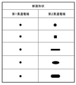
- FIG. 6 is a tabular explanatory view showing the cross-sectional shapes of the first through electrode and the second through electrode.
- FIG. 7A is an explanatory diagram of the expression that the figure is close to a circle.
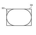
- FIG. 7B is an explanatory diagram of the expression that the figure is close to a rectangle.
- FIG. 8A is an explanatory diagram of a peripheral region in which a second through electrode is provided in a gap between a plurality of wirings.
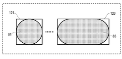
- FIG. 8B is an explanatory diagram of the shape of the through electrode.
- FIG. 9 is an explanatory diagram of the number density of the first through electrode and the number density of the second through electrode.
- FIG. 10A is an explanatory diagram of the arrangement interval of the second through silicon via.
- FIG. 10B is an explanatory diagram of the arrangement interval of the second through silicon via.
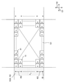
- FIG. 11A is an explanatory diagram of the number density of the third through electrode.
- FIG. 11B is an explanatory diagram of the number density of the fourth through electrode.
- FIG. 12A is an explanatory diagram of the arrangement interval of the third through electrode.
- FIG. 12B is an explanatory diagram of the arrangement interval of the fourth through electrode.
- FIG. 13A is an explanatory diagram showing a specific example of the arrangement of the through electrodes.
- FIG. 13B is an explanatory diagram showing a specific example of the arrangement of the through electrodes.
- FIG. 13C is an explanatory diagram showing a specific example of the arrangement of the through electrodes.
- FIG. 13D is an explanatory diagram showing a specific example of the arrangement of the through electrodes.
- FIG. 13E is an explanatory diagram showing a specific example of
- the image pickup apparatus is A pixel area including the first substrate portion and provided with a plurality of pixels, A peripheral region including a second substrate portion and not provided with pixels is provided. The first substrate portion and the second substrate portion are included in one semiconductor substrate. Each of the plurality of pixels With the first electrode With the second electrode A photoelectric conversion layer located between the first electrode and the second electrode, The charge storage region provided in the first substrate portion and including.
- the pixel area is A plurality of first through holes penetrating the first substrate portion, Each includes a plurality of first through electrodes provided in the corresponding first through holes of the plurality of first through holes and electrically connecting the first electrode and the charge storage region.
- the peripheral area is A plurality of second through holes penetrating the second substrate portion, Each includes a plurality of second through electrodes provided in the corresponding second through holes of the plurality of second through holes.
- the area density of the plurality of first through electrodes which is the ratio of the area of the plurality of first through electrodes to the area of the pixel region, is the ratio of the area of the plurality of second through electrodes to the area of the peripheral region. It is different from the area density of the plurality of second through electrodes.
- the technology according to the present disclosure is suitable for mass production of an image pickup device that meets the required specifications of the pixel region and the required specifications of the peripheral region.
- the image pickup apparatus is It is electrically separated from the plurality of first through electrodes and further includes an electrical path including the plurality of second through electrodes.
- the electric path may be electrically connected to a specific portion in the pixel region without passing through the first substrate portion.
- the second aspect it is easier to suppress crosstalk between the electric path and the first through electrode as compared with the case of forming the electric path to the specific portion via the first substrate portion.
- the image pickup apparatus further includes a shield electrode electrically separated from the first electrode.
- the photoelectric conversion layer may be located between the shield electrode and the second electrode.
- the specific portion may be included in the shield electrode or the second electrode.
- the shield electrode or the second electrode of the third aspect is an example of an element that can include the specific portion.
- the cross-sectional shape of each of the plurality of first through electrodes may be different from the cross-sectional shape of each of the plurality of second through electrodes.
- Making a difference in the cross-sectional shape of the through electrode as in the fourth aspect can contribute to the realization of the required specifications of the pixel region and the peripheral region.
- the cross-sectional shape of each of the plurality of first through electrodes may be closer to a circle than the cross-sectional shape of each of the plurality of second through electrodes.
- the cross-sectional shape of each of the plurality of second through electrodes may be closer to a rectangle than the cross-sectional shape of each of the plurality of first through electrodes.
- the peripheral region may further include a plurality of wirings located in the second substrate portion.
- the plurality of second through electrodes may pass between the plurality of wirings.
- the smallest area rectangle surrounding the cross-sectional shape of each of the plurality of first through electrodes has a first side and a second side having a length equal to or greater than the length of the first side.
- the smallest area rectangle surrounding the cross-sectional shape of each of the plurality of second through electrodes has a third side and a fourth side having a length equal to or greater than the length of the third side.
- the ratio of the length of the second side to the length of the first side is defined as the first ratio.
- When the ratio of the length of the fourth side to the length of the third side is defined as the second ratio,
- the first ratio may be smaller than the second ratio.
- the cross-sectional area of each of the plurality of first through electrodes may be different from the cross-sectional area of each of the plurality of second through electrodes.
- Making a difference in the cross-sectional area of the through electrode as in the seventh aspect can contribute to the realization of the required specifications of the pixel region and the peripheral region.
- the image pickup apparatus according to the seventh aspect is The cross-sectional area of each of the plurality of first through electrodes may be smaller than the cross-sectional area of each of the plurality of second through electrodes.
- the perimeter of each cross section of the plurality of first through electrodes may be different from the perimeter of each cross section of the plurality of second through electrodes.
- the perimeter of the cross section of each of the plurality of first through electrodes may be shorter than the perimeter of the cross section of each of the plurality of second through electrodes.
- the number density of the plurality of first through electrodes in the pixel region may be different from the number density of the plurality of second through electrodes in the peripheral region.
- Differentiating the number densities of the through electrodes as in the eleventh aspect can contribute to the realization of the required specifications of the pixel region and the peripheral region.
- the number density of the plurality of first through electrodes in the pixel region may be smaller than the number density of the plurality of second through electrodes in the peripheral region.
- the area density of the plurality of first through electrodes may be smaller than the area density of the plurality of second through electrodes.
- the material of the plurality of first through electrodes may be different from the material of the plurality of second through electrodes.
- Making a difference in the material of the through electrode as in the 14th aspect can contribute to the realization of the required specifications of the pixel region and the peripheral region.
- the plurality of first through electrodes may be substantially free of copper.
- the plurality of through silicon vias may contain copper as a main component.
- the fifteenth aspect is advantageous from the viewpoint of allowing a large current to flow between the element on the first surface side and the element on the second surface side of the second substrate portion in the peripheral region while avoiding the diffusion of copper in the pixel region. ..
- the peripheral region may include a first adjacent region adjacent to the pixel region in the first direction in a plan view and a second adjacent region adjacent to the pixel region in a second direction in a plan view.
- the ratio of the average value of the arrangement intervals of the plurality of second through electrodes in the first adjacent region to the average value of the arrangement intervals of the plurality of second through electrodes in the second adjacent region is 0.8 or more. It may be 2 or less.
- the 16th aspect it is easy to equalize the current supply capacity per unit length in the second direction of the first adjacent region and the current supply capacity per unit length in the first direction of the second adjacent region.
- the image pickup apparatus according to any one of the 1st to 16th aspects is A shield electrode electrically separated from the first electrode may be further provided.
- the plurality of second through electrodes may include at least one third through electrode and at least one fourth through electrode electrically separated from each other.
- the photoelectric conversion layer may be located between the shield electrode and the second electrode.
- the at least one through silicon via may be electrically connected to the shield electrode.
- connection destination of the third through electrode and the connection destination of the fourth through electrode can be electrically separated.
- the shield electrode and the element existing on the opposite side of the shield electrode when viewed from the second substrate portion can be electrically connected.
- the at least one through silicon via may be electrically connected to the second electrode.
- the second electrode and the element existing on the opposite side of the second electrode when viewed from the second substrate portion can be electrically connected.
- the at least one through silicon via includes a plurality of third through electrodes.
- the at least one through silicon via includes a plurality of fourth through electrodes.
- the number density of the plurality of third through electrodes in the peripheral region may be different from the number density of the plurality of fourth through electrodes in the peripheral region.
- the image pickup apparatus is A pixel area including the first substrate portion and provided with a plurality of pixels, A peripheral region including a second substrate portion and not provided with pixels is provided. The first substrate portion and the second substrate portion are included in one semiconductor substrate. Each of the plurality of pixels With the first electrode With the second electrode A photoelectric conversion layer located between the first electrode and the second electrode, The charge storage region provided in the first substrate portion and including.
- the pixel area is A plurality of first through holes penetrating the first substrate portion, Each includes a plurality of first through electrodes provided in the corresponding first through holes of the plurality of first through holes and electrically connecting the first electrode and the charge storage region.
- the peripheral area is A plurality of second through holes penetrating the second substrate portion, Each includes a plurality of second through electrodes provided in the corresponding second through holes of the plurality of second through holes.
- the cross-sectional area of each of the plurality of first through electrodes is smaller than the cross-sectional area of each of the plurality of second through electrodes.
- the peripheral region includes a first adjacent region adjacent to the pixel region along a first axis in a plan view, and a second adjacent region adjacent to the pixel region along a second axis in a plan view.
- the dimension of the first adjacent region along the second axis may be smaller than the dimension of the second adjacent region along the first axis.
- the average value of the arrangement intervals of the plurality of second through electrodes in the first adjacent region may be shorter than the average value of the arrangement intervals of the plurality of second through electrodes in the second adjacent region.
- the 21st aspect it is easy to equalize the current supply capacity of the first adjacent region as a whole and the current supply capacity of the second adjacent region as a whole.
- the cross-sectional shape of the at least one through silicon via may be different from the cross-sectional shape of the at least one through silicon via.
- Making a difference in the cross-sectional shape of the through electrode as in the 22nd aspect can contribute to the realization of the required specifications of the connection destination of the third through electrode and the connection destination of the fourth through electrode.
- the at least one through silicon via may include a plurality of third through electrodes.
- the at least one through silicon via may include a plurality of fourth through electrodes.
- the area density of the plurality of third through electrodes in the peripheral region may be different from the area density of the plurality of fourth through electrodes in the peripheral region.
- Differentiating the area density of the through electrodes as in the 23rd aspect can contribute to the realization of the required specifications of the connection destination of the third through electrode and the connection destination of the fourth through electrode.
- the peripheral region may have a first adjacent region adjacent to the pixel region in the first direction in a plan view.
- the at least one through silicon via may include a plurality of third through electrodes.
- the at least one through silicon via may include a plurality of fourth through electrodes. The average value of the arrangement intervals of the plurality of third through electrodes in the first adjacent region may be different from the average value of the arrangement intervals of the plurality of fourth through electrodes in the first adjacent region.
- Making a difference in the average arrangement interval of the through electrodes as in the 24th aspect can contribute to the realization of the required specifications of the connection destination of the third through electrode and the connection destination of the fourth through electrode.
- planar view means a view from the thickness direction of the first substrate portion or the thickness direction of the second substrate portion.
- the thickness direction of the first substrate portion or the thickness direction of the second substrate portion may be the same.
- a rectangle is a concept including a square.
- resistance refers to electrical resistance
- the principal component means the component contained most in terms of mass.
- the main component is a component exceeding 50% by mass. In one specific example, the main component is a component exceeding 80% by mass.
- substantially no inclusion means that the content is less than 1% by mass on a mass basis. In one embodiment, “substantially free” means that the content is less than 0.1% by mass on a mass basis.
- FIG. 1 is a configuration diagram of an image pickup apparatus according to an embodiment.
- the image pickup apparatus 100 shown in FIG. 1 includes a pixel area 101 and a peripheral area 102.
- the pixel area 101 has a first substrate portion.
- the peripheral region 102 has a second substrate portion.
- the first substrate portion is a first semiconductor substrate portion.
- the second substrate portion is a second semiconductor substrate portion.
- the first substrate portion and the second substrate portion are different portions in a plan view of one substrate.
- a configuration in which the first substrate portion is a substrate and the second substrate portion is another substrate may be adopted.
- Pixel 10 is provided in the pixel area 101.
- the pixel 10 has a photoelectric conversion unit.
- the photoelectric conversion unit converts the incident light into electric charges.
- a plurality of pixels 10 are provided.
- the plurality of pixels 10 constitute a pixel array PA.
- the plurality of pixels 10 are arranged two-dimensionally.
- the plurality of pixels 10 may be arranged one-dimensionally.
- the image pickup apparatus 100 may be a line sensor.
- the pixels 10 are arranged in a matrix of m rows and n columns.
- the center of each pixel 10 is located on a grid point of a square grid.
- the arrangement of the pixels 10 is not limited to the illustrated example.
- the center of each pixel 10 may be located on a grid point such as a triangular grid or a hexagonal grid.
- a peripheral circuit 90 is provided in the peripheral region 102.
- the peripheral circuit 90 controls the pixel 10.
- the peripheral circuit 90 includes a row scanning circuit 91, a signal processing circuit 92, an output circuit 93, and a control circuit 94.
- the row scanning circuit 91 is also called a vertical scanning circuit.
- the row scanning circuit 91 is connected to row control lines R 0 , R 1 , ..., Ri , ..., R m-1 .
- the row control lines R 0 , R 1 , ..., Ri , ..., R m-1 are associated with each row of the plurality of pixels 10.
- a row control line R i is connected to the plurality of pixels 10 belonging to the i-th row.
- the row scanning circuit 91 is connected to a plurality of pixels 10 belonging to the i-th row via the row control line R i .
- i is an arbitrary integer of 0 or more and m-1 or less.
- the row scanning circuit 91 selects the pixel 10 in row units, reads out the signal voltage, resets the photoelectric conversion unit in the pixel, and the like.
- FIG. 1 merely schematically shows the connection between each pixel 10 and the row scanning circuit 91.
- the number of control lines arranged for each row of the plurality of pixels 10 is not limited to one.
- the image pickup apparatus 100 may have two or more control lines for each row.
- the row scanning circuit 91 may be connected to a plurality of reset control lines, and a reset control line associated with the row may be connected to each row of the plurality of pixels 10.
- the signal processing circuit 92 is connected to the output signal lines S 0 , S 1 , ..., S j , ..., S n-1 .
- the output signal lines S 0 , S 1 , ..., S j , ..., S n-1 are each associated with each column of the plurality of pixels 10.
- the output signal line Sj is connected to the plurality of pixels 10 belonging to the jth column.
- the signal processing circuit 92 is connected to a plurality of pixels 10 belonging to the jth column via the output signal line S j .
- j is an arbitrary integer of 0 or more and n-1 or less.
- the output of the pixel 10 is selected line by line by the line scanning circuit 91, and is read from the output signal line S 0 to the signal processing circuit 92 via the output signal line S n-1 .
- the signal processing circuit 92 performs noise suppression signal processing, analog-to-digital conversion, and the like on the output signal read from the pixel 10.
- An example of noise suppression signal processing is correlated double sampling.
- the output of the signal processing circuit 92 is read out to the outside of the image pickup apparatus 100 via the output circuit 93.
- command data a clock, and the like are given to the control circuit 94 from the outside of the image pickup apparatus 100.
- the control circuit 94 controls the entire image pickup apparatus 100 based on these.
- control circuit 94 has a timing generator. Then, the control circuit 94 supplies a drive signal to the row scanning circuit 91, the signal processing circuit 92, and the like.
- FIG. 2 is a schematic cross-sectional view showing the device structures of the pixel region 101 and the peripheral region 102.
- first conductive type may be used.
- the first conductive type is n type.
- the second conductive type is a p type.
- the first conductive type may be a p type.
- the second conductive type may be n type.
- the pixel 10 includes an insulating layer 71, an insulating layer 70, a first substrate unit 1, an insulating layer 32, a photoelectric conversion unit 12, an insulating layer 31, a color filter 35, and a microlens 30. There is.
- the insulating layer 71, the insulating layer 70, the first substrate portion 1, the insulating layer 32, the photoelectric conversion unit 12, the insulating layer 31, the color filter 35, and the microlens 30 are laminated in this order. .. Specifically, these are laminated in the thickness direction of the first substrate portion 1.
- the pixel 10 includes a first through electrode 81, an insulating layer 33, and a shield electrode 16.
- the first substrate portion 1 is, for example, a part of a silicon substrate.
- the first substrate portion 1 has a first main surface 1A and a second main surface 1B.
- the first main surface 1A is the back surface.
- the first main surface 1A is a surface on the side on which light is incident.
- the second main surface 1B is a surface.
- the second main surface 1B is a surface opposite to the side on which light is incident.
- the first main surface 1A and the second main surface 1B extend perpendicularly to the thickness direction of the first substrate portion 1.
- the first substrate portion 1 includes a second conductive type impurity region 1i.
- the impurity region 1i can be, for example, a p + region or an n + region. “+” Indicates that the concentration of p-type or n-type impurities is high.
- the impurity region 1i has a first main surface 1A.
- the impurity region 1i has a part of the first main surface 1B.
- the first board portion 1 is provided with a reset transistor 26, a signal detection transistor 22, and a transfer transistor 28. Specifically, these reset transistor 26, signal detection transistor 22 and transfer transistor 28 are provided on the second main surface 1B.
- the reset transistor 26, the signal detection transistor 22, and the transfer transistor 28 are MOSFETs (Metal Oxide Semiconductor Field Effect Transistor). Specifically, these reset transistor 26, signal detection transistor 22 and transfer transistor 28 are N-channel MOSFETs.
- the reset transistor 26 includes the first diffusion region 67n as one of the source and the drain.
- the reset transistor 26 includes a second diffusion region 68an as the other of the source and drain. Further, the reset transistor 26 includes a gate electrode 26e and an insulating layer 70. The insulating layer 70 is interposed between the gate electrode 26e and the first substrate portion 1.
- the signal detection transistor 22 includes a third diffusion region 68 bn as one of a source and a drain.
- the signal detection transistor 22 includes a fourth diffusion region 68 cn as the other of the source and drain.
- the signal detection transistor 22 includes a gate electrode 22e and an insulating layer 70.
- the insulating layer 70 is interposed between the gate electrode 22e and the first substrate portion 1.
- the signal detection transistor 22 can also be referred to as an amplification transistor.
- the transfer transistor 28 includes a fifth diffusion region 68dn as one of a source and a drain. The other of the source and drain of the transfer transistor 28 is connected to the photodiode 27. Further, the transfer transistor 28 includes a gate electrode 28e and an insulating layer 70. The insulating layer 70 is interposed between the gate electrode 28e and the first substrate portion 1.
- the first diffusion region 67n, the second diffusion region 68an, the third diffusion region 68bn, the fourth diffusion region 68cn, and the fifth diffusion region 68dn are located in the first substrate portion 1.
- the first diffusion region 67n, the second diffusion region 68an, the third diffusion region 68bn, the fourth diffusion region 68cn, and the fifth diffusion region 68dn contain first conductive type impurities.
- the first diffusion region 67n corresponds to the charge storage region FD.
- the first diffusion region 67n accumulates the electric charge generated by the photoelectric conversion in the photoelectric conversion unit 12.
- the charge storage region FD may be referred to as a first charge storage region FD.
- the fifth diffusion region 68dn corresponds to the second charge storage region FD2.
- the fifth diffusion region 68dn stores the charge generated by the photoelectric conversion in the photodiode 27.
- the photoelectric conversion unit 12 has a pixel electrode 13, a photoelectric conversion layer 14, and a counter electrode 15.
- the facing electrode 15 faces the pixel electrode 13.
- the photoelectric conversion layer 14 is arranged between the pixel electrode 13 and the counter electrode 15.
- the photoelectric conversion layer 14 has a film shape.
- the photoelectric conversion layer 14 contains at least one selected from the group consisting of an organic material and an inorganic material. Amorphous silicon is exemplified as an inorganic material.
- the photoelectric conversion layer 14 receives the light incident through the counter electrode 15 and generates positive and negative charges by photoelectric conversion.
- the photoelectric conversion layer 14 is typically formed over a plurality of pixels 10.
- the photoelectric conversion layer 14 may include a layer made of an organic material and a layer made of an inorganic material.
- the counter electrode 15 is a transparent electrode. Specifically, the counter electrode 15 is an electrode made of a transparent conductive material such as ITO (Indium Tin Oxide). The counter electrode 15 is arranged on the light receiving surface side of the photoelectric conversion layer 14. The counter electrode 15 is typically formed over a plurality of pixels 10, similarly to the photoelectric conversion layer 14.
- ITO Indium Tin Oxide
- the potential of the counter electrode 15 is controlled to make the potential of the counter electrode 15 different from the potential of the pixel electrode 13, so that the signal charge generated by the photoelectric conversion is collected by the pixel electrode 13. Can be done.
- the signal charge is a negative charge, specifically an electron.
- the potential of the counter electrode 15 is controlled so that the potential of the counter electrode 15 is lower than the potential of the pixel electrode 13.
- electrons can be collected by the pixel electrode 13.
- the signal charge collected by the pixel electrode 13 is accumulated in the first diffusion region 67n via the first through electrode 81 and the wiring structure 80.
- the signal charge is a positive charge, specifically a hole.
- the potential of the counter electrode 15 is typically controlled so that the potential of the counter electrode 15 is higher than the potential of the pixel electrode 13.
- holes can be collected by the pixel electrode 13.
- the signal charge collected by the pixel electrode 13 is accumulated in the first diffusion region 67n via the first through electrode 81 and the wiring structure 80.
- the pixel electrode 13 is a transparent electrode. Specifically, the pixel electrode 13 is an electrode made of a transparent conductive material such as ITO. The pixel electrode 13 is electrically separated from the pixel electrode 13 of the other pixel 10 by being spatially separated from the pixel electrode 13 of the other adjacent pixel 10.
- the shield electrode 16 is located on the same side as the pixel electrode 13 when viewed from the photoelectric conversion layer 14. However, the shield electrode 16 is separated from the pixel electrode 13. The shield electrode 16 is electrically separated from the pixel electrode 13.
- the shield electrode 16 includes a portion located between the pixel electrode 13 in a certain pixel 10 and the pixel electrode 13 in a pixel 10 adjacent to the pixel 10. Then, the portion of the shield electrode 16 collects the electric charge generated by the photoelectric conversion in the photoelectric conversion layer 14. In this way, the shield electrode 16 can suppress noise from being mixed into the charge storage region FD.
- the material of the shield electrode 16 a material that can be used as the material of the pixel electrode 13 can be adopted.
- the material of the shield electrode 16 may be the same as the material of the pixel electrode 13, or may be different from the material of the pixel electrode 13.
- FIG. 3 is a plan view showing the shield electrode 16.
- the shield electrode 16 has a grid shape. Pixel electrodes 13 are arranged in each space partitioned by this grid shape. The grid shape extends across the plurality of pixels 10. In FIG. 3, some of the elements of the image pickup apparatus 100 are not shown.
- the microlens 30 has a light-collecting action.
- the light incident on the microlens 30 is supplied to the photoelectric conversion unit 12 via the color filter 35.
- the photoelectric conversion unit 12 converts the light supplied in this way into electric charges.
- the insulating layer 31 is provided between the color filter 35 and the photoelectric conversion unit 12.
- the insulating layer 31 functions as a protective layer that protects the photoelectric conversion unit 12.
- the insulating layer 32 is provided between the pixel electrode 13 and the first substrate portion 1. Further, the insulating layer 32 is provided between the shield electrode 16 and the first substrate portion 1.
- the photodiode 27 and the well 29 are provided in the first substrate portion 1.
- the photodiode 27 is a first conductive type.
- the well 29 is a second conductive type. As shown in FIG. 2, in a cross section parallel to the thickness direction of the first substrate portion 1, the impurity region 1i is bent to form a recess, and the photodiode 27 is in the recess.
- the well 29 is provided with a through hole, and the first through electrode 81 is provided in the through hole.
- the photodiode 27 exhibits sensitivity to light.
- the photodiode 27 is provided in the first substrate portion 1.
- the photodiode 27 photoelectrically converts light in a wavelength range of a color that has not been absorbed by the photoelectric conversion unit 12.
- the photodiode 27 When the photodiode 27 is irradiated with light, an electric charge is generated in the photodiode 27. The generated charge is stored as a signal charge in the photodiode 27. In this embodiment, the signal charge is a negative charge. Specifically, the signal charge is an electron.
- the photodiode 27 is a first conductive type impurity layer. It should be noted that a configuration in which a positive charge, specifically a hole, is used as the signal charge from the photodiode 27 can also be adopted.
- the transfer transistor 28 transfers the signal charge stored in the photodiode 27 to the second charge storage region FD2.
- a transfer signal line is connected to the gate electrode 28e of the transfer transistor 28.
- the transfer transistor 28 can be turned on by applying a transfer signal for controlling the on and off of the transfer transistor 28 to the gate electrode 28e via the transfer signal line.
- the transfer transistor 28 is turned on, the signal charge stored in the photodiode 27 is transferred to the second charge storage region FD2.
- a wiring structure 80 is provided in the insulating layer 71.
- the wiring structure 80 includes a first wiring 80a and a second wiring 80b.
- the wiring structure 80 typically comprises at least one selected from the group consisting of metals and metal compounds.
- the metal include copper and tungsten.
- the metal compound include metal nitrides and metal oxides. The same can be said for the first wiring 80a and the first wiring 80b.
- a first contact plug cp1, a second contact plug cp2, a third contact plug cp3, a fourth contact plug cp4, a fifth contact plug cp5, a sixth contact plug cp6, and the like 7 contact plug cp7 and 7 contact plugs cp7 are provided.
- a gate electrode 26e, a gate electrode 22e, and a gate electrode 28e are provided in the insulating layer 71.
- the first contact plug cp1, the second contact plug cp2, the third contact plug cp3, the fourth contact plug cp4, the fifth contact plug cp5, the sixth contact plug cp6 and the seventh contact plug cp7 are semiconductor materials. Includes.
- the first contact plug cp1, the second contact plug cp2, the third contact plug cp3, the fourth contact plug cp4, the fifth contact plug cp5, the sixth contact plug cp6, and the seventh contact plug cp7 are the first. It is a polysilicon layer doped with conductive impurities.
- the semiconductor materials contained in the first contact plug cp1, the second contact plug cp2, the third contact plug cp3, the fourth contact plug cp4, the fifth contact plug cp5, the sixth contact plug cp6, and the seventh contact plug cp7 are It may be polycrystalline silicon, germanium or the like. Further, the first contact plug cp1, the second contact plug cp2, the third contact plug cp3, the fourth contact plug cp4, the fifth contact plug cp5, the sixth contact plug cp6 and the seventh contact plug cp7 may be used together with the semiconductor material or. Instead of a semiconductor material, it may contain a metal.
- the first substrate portion 1 is provided with a first through hole 82. Specifically, openings are provided in the first main surface 1A and the second main surface 1B of the first substrate portion 1, and the first through hole 82 connects these openings. Specifically, the first through hole 82 extends along the thickness direction of the first substrate portion 1.
- the first through hole 82 is provided with a first through electrode 81.
- the first through electrode 81 may electrically connect elements separated in the thickness direction of the first substrate portion 1 by the first substrate portion 1.
- the first through silicon via 81 typically comprises at least one selected from the group consisting of metals and metal compounds.
- the metal include copper and tungsten.
- the metal compound include metal nitrides and metal oxides.
- the first through electrode 81 may contain the same semiconductor material as the material contained in the first substrate portion 1, and may be injected with impurities of the first conductive type or the second conductive type.
- the semiconductor material that the first substrate portion 1 and the first through silicon via 81 can include include silicon, polycrystalline silicon, germanium, and the like.
- the insulating layer 33 is provided along the direction in which the first through silicon via 81 extends. In a plan view, the insulating layer 33 surrounds the first through silicon via 81. Specifically, in a plan view, the insulating layer 33 surrounds the first through silicon via 81 without a gap.
- the pixel electrode 13, the first through electrode 81, the first contact plug cp1, the second wiring 80b, the second contact plug cp2, and the charge storage region FD are electrically connected in this order. Therefore, the signal charge passes from the pixel electrode 13 through the first through electrode 81, the first contact plug cp1, the second wiring 80b, and the second contact plug cp2 in this order to the charge storage region FD. Can be sent. Specifically, holes or electrons as signal charges are sent from the pixel electrode 13 to the first through electrode 81, the first contact plug cp1, the second wiring 80b, and the second contact plug cp2 in this order. It can be sent through to the charge storage region FD.
- the charge storage region FD, the second contact plug cp2, the second wiring 80b, the fifth contact plug cp5, and the gate electrode 22e of the signal detection transistor 22 are electrically connected in this order. Therefore, the signal charge can be sent from the charge storage region FD to the gate electrode 22e through the second contact plug cp2, the second wiring 80b, and the fifth contact plug cp5 in this order.
- the third contact plug cp3 electrically connects the second diffusion region 68an and the first wiring 80a. Therefore, the electric charge can be sent from the second diffusion region 68an to the first wiring 80a through the third contact plug cp3.
- the third diffusion region 68bn and the fourth contact plug cp4 are electrically connected. Therefore, electric charges can flow between the third diffusion region 68bn and the fourth contact plug cp4.
- the wiring connected to the fourth contact plug cp4 is not shown.
- the fourth diffusion region 68cn and the sixth contact plug cp6 are electrically connected. Therefore, electric charges can flow between the fourth diffusion region 68cn and the sixth contact plug cp6.
- the wiring connected to the sixth contact plug cp6 is not shown.
- the fifth diffusion region 68dn that is, the second charge storage region FD2 and the seventh contact plug cp7 are electrically connected. Therefore, electric charges can flow between the fifth diffusion region 68dn and the seventh contact plug cp7.
- the wiring connected to the 7th contact plug cp7 is not shown.
- the first through electrode 81 is connected to the second wiring 80b via the first contact plug cp1.
- the first through electrode 81 may be directly connected to the second wiring 80b.
- the first through electrode 81 is directly connected to the pixel electrode 13.
- the first through electrode 81 may be connected to the pixel electrode 13 via a plug or the like.
- the peripheral region 102 includes an insulating layer 73, an insulating layer 72, and a second substrate portion 2.
- the insulating layer 73, the insulating layer 72, and the second substrate portion 2 are laminated in this order. Specifically, these are laminated in the thickness direction of the second substrate portion 2. Further, the peripheral region 102 includes a second through electrode 83 and a connection electrode 17.
- the second substrate portion 2 is, for example, a part of a silicon substrate.
- the second substrate portion 2 has a first main surface 2A and a second main surface 2B.
- the first main surface 2A is the back surface.
- the second main surface 2B is a surface.
- the first main surface 2A and the second main surface 2B extend perpendicularly to the thickness direction of the second substrate portion 2.
- a third wiring 80c, a fourth wiring 80d, an eighth contact plug cp8, and a ninth contact plug cp9 are provided.
- the material of the third wiring 80c and the fourth wiring 80d a material that can be used as the material of the first wiring 80a and the second wiring 80b can be adopted.
- the first contact plug cp1 As materials for the 8th contact plug cp8 and the 9th contact plug cp9, the first contact plug cp1, the second contact plug cp2, the third contact plug cp3, the fourth contact plug cp4, the fifth contact plug cp5, and the sixth contact plug cp6. And a material that can be used as the material of the 7th contact plug cp7 can be used.
- the second substrate portion 2 is provided with a second through hole 87. Specifically, openings are provided in the first main surface 2A and the second main surface 2B of the second substrate portion 2, and the second through hole 87 connects these openings. Further, specifically, the second through hole 87 extends along the thickness direction of the second substrate portion 2.
- the second through hole 87 is provided with a second through electrode 83.
- the second through electrode 83 can electrically connect elements separated in the thickness direction of the second substrate portion 2 by the second substrate portion 2.
- the material of the second through electrode 83 As the material of the second through electrode 83, a material that can be used as the material of the first through electrode 81 can be adopted.
- connection electrode 17 As the material of the connection electrode 17, a material that can be used as the shield electrode 16 or the counter electrode 15 can be used.
- an insulating layer similar to the insulating layer 33 may surround the second through silicon via 83.
- the first through electrode 81 and the second through electrode 83 are electrically separated.
- the second substrate portion 2 is provided with a plurality of second through holes 87. There are a plurality of second through electrodes 83. There are a plurality of connection electrodes 17.
- the plurality of second through holes 87 include at least one third through hole 88 and at least one fourth through hole 89.
- the plurality of through silicon vias 83 includes at least one through silicon via 84 and at least one through silicon via 85.
- the plurality of connection electrodes 17 include at least one first connection electrode 18 and at least one second connection electrode 19.
- the third wiring 80c, the eighth contact plug cp8, the third through electrode 84, the first contact electrode 18, and the shield electrode 16 are electrically connected in this order.
- a voltage can be supplied to the shield electrode 16 via the third wiring 80c, the eighth contact plug cp8, the third through electrode 84, and the first connection electrode 18 in this order.
- the voltage supplied to the shield electrode 16 may be referred to as a shield voltage.
- FIG. 3 shows a specific example of electrical connection between the third through electrode 84 and the shield electrode 16 via the first connection electrode 18.
- the first connection electrode 18 is provided so as to surround the shield electrode 16 in a plan view, and a plurality of third through electrodes 84 are connected to the first connection electrode 18.
- the “x” mark in FIG. 3 schematically shows the third through electrode 84 in a plan view.
- the shield electrode 16 and the first connection electrode 18 are electrically connected, but there is a connection mark between them.
- the shield electrode 16 and the first connection electrode 18 may be an integral electrode having no connection mark between them.
- the fourth wiring 80d, the ninth contact plug cp9, the fourth through electrode 85, the second connecting electrode 19, and the counter electrode 15 are electrically connected in this order.
- a voltage can be supplied to the counter electrode 15 via the fourth wiring 80d, the ninth contact plug cp9, the fourth through electrode 85, and the second connection electrode 19 in this order.
- the voltage supplied to the counter electrode 15 may be referred to as a counter voltage.
- FIG. 4A is a cross-sectional view showing a specific example of the electrical connection between the fourth through electrode 85 and the counter electrode 15.
- FIG. 4B is a plan view showing the specific example.
- FIG. 4C is a cross-sectional view showing another specific example of the electrical connection between the fourth through electrode 85 and the counter electrode 15.
- FIG. 4D is a plan view showing another specific example.
- the first substrate portion 1 and the second substrate portion 2 are different parts in a plan view of one common substrate.
- some of the elements of the image pickup apparatus 100 are not shown.
- the shield electrode 16 is not shown.
- the “x” marks in FIGS. 4B and 4D schematically indicate the fourth through silicon via 85 in a plan view.
- the counter electrode 15 is provided so as to straddle the boundary between the pixel region 101 and the peripheral region 102.
- the portion of the counter electrode 15 that straddles the boundary between the pixel region 101 and the peripheral region 102 approaches the common substrate as it progresses from the pixel region 101 side to the peripheral region 102 side.
- the portion of the counter electrode 15 belonging to the peripheral region 102 is connected to the fourth through electrode 85 via the second connecting electrode 19.
- the wiring layer 96 is provided so as to straddle the boundary between the pixel area 101 and the peripheral area 102.
- the counter electrode 15 and the fourth through electrode 85 are electrically connected via the wiring layer 96 and the second connection electrode 19.
- the insulating layer 97 is arranged on the counter electrode 15 in the pixel region 101.
- the insulating layer 97 is provided with a through hole 97a.
- the wiring layer 96 is in contact with the upper surface of the counter electrode 15 by entering the through hole 97a. Further, the wiring layer 96 is in contact with the side surface of the counter electrode 15. In this way, the wiring layer 96 is electrically connected to the counter electrode 15.
- the first substrate portion 1 and the second substrate portion 2 are portions of one substrate that are different from each other in a plan view.
- the first main surface 1A and the first main surface 2A are continuous.
- the second main surface 1B and the second main surface 2B are continuous.
- the insulating layer 70 and the insulating layer 72 may be an integral layer of the same material.
- the insulating layer 71 and the insulating layer 73 may be an integral layer of the same material.
- the wiring structure 80 includes the third wiring 80c and the fourth wiring 80d together with the first wiring 80a and the second wiring 80b.
- the first wiring 80a, the second wiring 80b, the third wiring 80c, and the fourth wiring 80c form a wiring layer.
- the wiring structure 80 may have a plurality of wiring layers.
- the terms first electrode and second electrode will be used.
- the first electrode corresponds to the pixel electrode 13.
- the second electrode corresponds to the counter electrode 15.
- the above-mentioned characteristics of the pixel electrode 13 can be applied to the first electrode.
- the above-mentioned characteristics of the counter electrode 15 can be applied to the second electrode.
- the image pickup apparatus 100 includes a pixel area 101 and a peripheral area 102. Pixels 10 are provided in the pixel area 101. A peripheral circuit 90 is provided in the peripheral region 102. The peripheral circuit 90 controls the pixel 10.
- the pixel region 101 has a first substrate portion 1.
- the pixel 10 has a first electrode, a second electrode, a photoelectric conversion layer 14, a charge storage region FD, a first through hole 82, and a first through electrode 81.
- the photoelectric conversion layer 14 is located between the first electrode and the second electrode.
- the charge storage region FD is provided in the first substrate portion 1.
- the first through hole 82 penetrates the first substrate portion 1.
- the first through electrode 81 is provided in the first through hole 82.
- the first through electrode 81 electrically connects the first electrode and the charge storage region FD.
- the peripheral region 102 has a second substrate portion 2, a second through hole 87, and a second through electrode 83.
- the second through hole 87 penetrates the second substrate portion 2.
- the second through electrode 83 is provided in the second through hole 87.
- the element on the first surface side and the element on the second surface side of the first substrate portion 1 can be electrically connected in the pixel region 101.
- the through silicon via 83 the element on the first surface side and the element on the second surface side of the second substrate portion 2 can be electrically connected in the peripheral region 102.
- the first through electrode 81 and the second through electrode 83 have the same basic configuration in that they are through electrodes. On the other hand, there is a degree of freedom in the design of through electrodes. Therefore, it is possible to adjust the design of the first through electrode 81 according to the required specifications of the pixel region 101 and adjust the design of the second through electrode 83 according to the required specifications of the peripheral region 102. Therefore, in the configuration in which the first through electrode 81 is provided in the pixel region 101 and the second through electrode 83 is provided in the peripheral region 102, the image pickup device 100 that satisfies the required specifications of the pixel region 101 and the required specifications of the peripheral region 102 is mass-produced. It is advantageous from the viewpoint of
- the first through electrode 81 can be designed in consideration of the electric charge obtained by photoelectric conversion flowing through the first through electrode 81 as a signal.
- the second through electrode 83 can be designed in consideration of the fact that the peripheral region 102 has the peripheral circuit 90.
- the pixel area 101 will be described.
- the pixel region 101 refers to a region overlapping the one first electrode in a plan view.
- the pixel region 101 refers to a region overlapping the smallest rectangle surrounding the plurality of first electrodes in a plan view.
- the image pickup apparatus 100 may be provided with a dummy electrode that is not electrically connected to the charge storage region.
- the region where the first electrode is not distributed and the dummy electrode is distributed does not correspond to the pixel region 101.
- the first substrate portion 1 and the second substrate portion 2 are each a part of a silicon substrate.
- the first through electrode 81 and the second through electrode 83 can enjoy the merits based on TSV (Through Silicon Via) in both the pixel region 101 and the peripheral region 102.
- the peripheral area 102 will be described.
- the peripheral region 102 is adjacent to the pixel region 101 in a plan view.
- the first substrate portion 1 and the second substrate portion 2 are each a part of a single semiconductor substrate.
- 5A and 5B are plan views showing an example of the pixel region 101 and the peripheral region 102.
- the peripheral region 102 in a plan view, extends in one direction of the first axis 131 and one direction of the second axis 132 when viewed from the pixel region 101.
- the peripheral region 102 in a plan view, extends on both sides along the first axis 131 and on both sides along the second axis 132 when viewed from the pixel region 101.
- FIG. 5C is an exploded perspective view showing a pixel region 101 and a peripheral region 102 related to such a form.
- the first substrate portion 1 and the second substrate portion 2 are separate semiconductor substrates laminated with each other.
- the image pickup device 100 of FIG. 5C may be a chip stack image pickup device.
- the first axis 131 and the second axis 132 are different axes from each other.
- the first axis 131 and the second axis 132 may be orthogonal to each other.
- the plurality of pixels 10 constitute a pixel array PA.
- the first axis 131 is parallel to one of the rows and columns of the pixel array PA.
- the second axis 132 is parallel to the other of the rows and columns of the pixel array PA.
- the first axis 131 is parallel to the row of the pixel array PA.
- the second axis 132 is parallel to the row of pixel array PAs.
- the first axis 131 may be parallel to the column of the pixel array PA and the second axis 132 may be parallel to the row of the pixel array PA.
- the expression "the first through electrode 81 is provided in the first through hole 82" will be described. This expression includes a form in which the first through electrode 81 extends in the first through hole 82 without protruding from the first through hole 82. This expression includes a form in which the first through electrode 81 extends beyond the first through hole 82. These points are the same for the expression "the second through electrode 83 is provided in the second through hole 87".
- the charge storage region FD is the first diffusion region 67n.
- the charge storage region FD is one of the source and drain of the reset transistor 26.
- the reset transistor 26 can reset the potential of the charge storage region FD.
- the image pickup apparatus 100 includes a shield electrode 16.
- the shield electrode 16 is electrically separated from the first electrode.
- the photoelectric conversion layer 14 is located between the shield electrode 16 and the second electrode.
- the first through electrode 81 is electrically separated from the electric path including the second through electrode 83, and the electric path bypassing the first substrate portion 1 and reaching a specific portion in the pixel region 101 is provided. It is configured. This electric path does not pass through the first substrate portion.
- the specific portion belongs to the pixel area 101. Therefore, it is conceivable to construct an electric path to the specific portion via the first substrate portion 1. However, if this is done, crosstalk may occur between the electric path and the first through silicon via 81, and noise may be superimposed on the electric charge flowing through the first through silicon via 81. However, when the electric path that bypasses the first substrate portion 1 and reaches the specific portion is configured, the electric path and the first are as compared with the case where the electric path that reaches the specific portion via the first substrate portion 1 is configured. It is easy to suppress crosstalk with the through electrode 81.
- the specific portion can be any portion in the pixel area 101.
- the shield electrode 16 includes a specific site.
- the second electrode comprises the specific site.
- FIGS. 3, 4A and 4C examples of specific portions are shown by reference numerals SP.
- the shapes of the first through electrode 81 and the second through electrode 83 are not particularly limited.
- the cross-sectional shapes of the first through electrode 81 and the second through electrode 83 are, for example, a circle, an ellipse, a polygon, a polygon with rounded corners, and the like.
- the polygon is a triangle, a quadrangle, a pentagon, a hexagon, or the like.
- FIG. 6 is a tabular explanatory view showing an example of the cross-sectional shape of the first through silicon via 81 and the second through silicon via 83.
- the cross-sectional shape of the first through silicon via 81 is different from the cross-sectional shape of the second through silicon via 83. Making a difference in the cross-sectional shapes of the first through electrode 81 and the second through electrode 83 in this way can contribute to the realization of the required specifications of the pixel region 101 and the peripheral region 102.
- the cross-sectional shape of the first through electrode 81 refers to the shape of the first through electrode 81 in the cross section perpendicular to the thickness direction of the first substrate portion 1 and passing through the first through electrode 81.
- the cross-sectional shape of the second through electrode 83 refers to the shape of the second through electrode 83 in the cross section perpendicular to the thickness direction of the second substrate portion 2 and passing through the second through electrode 83. "Different shapes" means that the figures mentioned are neither congruent nor similar.
- the cross-sectional shape of the first through silicon via 81 is closer to a circle than the cross-sectional shape of the second through silicon via 83.
- the cross-sectional shape of the second through silicon via 83 is closer to a rectangle than the cross-sectional shape of the first through silicon via 81.
- the electric charge obtained by the photoelectric conversion in the photoelectric conversion layer 14 flows through the first through electrode 81 as a signal.
- the cross-sectional shape of the first through silicon via 81 is relatively close to a circle. Therefore, it is easy to realize the first through electrode 81, which has a small cross-sectional area and is unlikely to cause crosstalk with other through electrodes, electric paths such as wiring, and the like. This is advantageous from the viewpoint of suppressing the superimposition of noise on the electric charge flowing through the first through silicon via 81.
- the first through electrode 81 having a small cross-sectional area can be realized. Further, this is advantageous from the viewpoint of securing a space for arranging an element such as a photodiode in the first substrate portion 1.
- the cross-sectional shape of the second through electrode 83 is relatively close to a rectangle. This may be advantageous in realizing the second through silicon via 83 having a large cross-sectional area and a low resistance. According to the second through electrode 83 having a small resistance, a large current can easily flow between the element on the first surface side and the element on the second surface side of the second substrate portion 2. The ability to pass a large current may be advantageous from the viewpoint of operating the device at high speed and stably.
- a laser beam may be used in the process of forming a through hole in the substrate portion.
- the through hole having a rectangular cross-sectional shape in design is formed in a small size and the case where the through hole is formed in a large size.
- the cross-sectional shape of the actually formed through hole tends to be closer to a circle than the design.
- the cross-sectional shape of the through hole actually formed tends to be a shape close to a rectangle because the design is well reflected.
- the design cross-sectional shapes of the first through electrode 81 and the second through electrode 83 the same, the first through electrode 81 and the second through electrode 83 actually manufactured have a cross-sectional shape. You may make a difference.
- FIG. 7A is an explanatory diagram of this expression.
- the fact that a certain figure 301 is close to a circle means that the ratio S 301 / S 302 of the area S 301 of the figure 301 to the area S 302 of the smallest circle 302 surrounding the figure 301 is large.
- FIG. 7B is an explanatory diagram of this expression.
- a figure 303 is close to a rectangle, it means that the ratio S 303 / S 304 of the area S 303 of the figure 303 to the area S 304 of the smallest rectangle 304 surrounding the figure 303 is large.
- FIG. 8A is an explanatory diagram of a peripheral region 102 in which a second through electrode 83 is provided in a gap between a plurality of wirings.
- FIG. 8B is an explanatory diagram of the shape of the through electrode.
- the peripheral region 102 includes a plurality of wirings 111 and 112 located in the second substrate portion 2.
- the through silicon via 83 passes through the gap 115 between the plurality of wirings 111 and 112.
- FIG. 8B shows a rectangle 121 having the smallest area surrounding the cross-sectional shape of the first through silicon via 81.
- FIG. 8B shows a rectangle 123 having the smallest area surrounding the cross-sectional shape of the second through silicon via 83.
- a side having a length equal to or longer than the length of the first side is defined as a second side.
- the ratio of the length of the second side to the length of the first side in the rectangle 121 is defined as the first ratio.
- the ratio of the length of the second side to the length of the first side in the rectangle 123 is defined as the second ratio.
- the first ratio is smaller than the second ratio.
- the electric charge obtained by the photoelectric conversion in the photoelectric conversion layer 14 can flow through the first through electrode 81 as a signal.
- the first ratio with respect to the first through silicon via 81 is relatively small. Therefore, it is easy to realize the first through silicon via 81 having a small cross-sectional area. This is advantageous from the viewpoint of suppressing the superimposition of noise on the electric charge flowing through the first through silicon via 81, as described above.
- a plurality of wirings 111 and 112 are provided as in the examples of FIGS. 8A and 8B, and the second through electrode 83 is provided so as to pass through the gap 115 between the wirings 111 and 112. May be constrained to place.
- the second ratio with respect to the second through silicon via 83 is relatively large. This may be advantageous in realizing the second through silicon via 83 having a large cross-sectional area and therefore a low resistance while satisfying the above constraints.
- the second through electrode 83 having a small resistance a large current can easily flow between the element on the first surface side and the element on the second surface side of the second substrate portion 2.
- the first side can be the short side of a rectangle.
- the first side can be one side of the square.
- the second side can be the long side of the rectangle.
- the second side can be one side of the square.
- the wirings 111 and 112 are, for example, signal lines.
- the cross-sectional shape of the first through silicon via 81 may be the same as the cross-sectional shape of the second through silicon via 83. "Same shape" means that the figures mentioned are in a congruent or similar relationship.
- the cross-sectional shape of the second through silicon via 83 may be closer to a rectangle than the cross-sectional shape of the first through silicon via 81.
- the cross-sectional shape of the first through silicon via 81 may be closer to a circle than the cross-sectional shape of the second through silicon via 83.
- the smallest rectangle surrounding the cross-sectional shape of the first through electrode 81 has a smaller ratio of the length of the second side to the length of the first side than the smallest rectangle surrounding the cross-sectional shape of the second through electrode 83. You may.
- the cross-sectional area of the first through electrode 81 is different from the cross-sectional area of the second through electrode 83.
- Such a difference in the cross-sectional areas of the through electrodes 81 and 83 can contribute to the realization of the required specifications of the pixel region 101 and the peripheral region 102.
- the cross-sectional area of the first through electrode 81 refers to the cross-sectional area of the first through electrode 81 in the cross section perpendicular to the thickness direction of the first substrate portion 1 and passing through the first through electrode 81.
- the cross-sectional area of the second through electrode 83 refers to the cross-sectional area of the second through electrode 83 in the cross section perpendicular to the thickness direction of the second substrate portion 2 and passing through the second through electrode 83.
- the cross-sectional area of the first through silicon via 81 is smaller than the cross-sectional area of the second through silicon via 83. This means that the elements on the first surface side and the elements on the second surface side of the second substrate portion 2 in the peripheral region 102 are suppressed while suppressing the superimposition of noise on the electric charge flowing through the first through electrode 81 in the pixel region 101. It is advantageous from the viewpoint of passing a large current between the two.
- the cross-sectional area of the first through electrode 81 may be larger than the cross-sectional area of the second through electrode 83.
- the cross-sectional area of the first through silicon via 81 may be the same as the cross-sectional area of the second through silicon via 83.
- a laser beam may be used in the process of forming a through hole in the substrate portion.
- a plurality of through holes having the same cross-sectional area are formed densely and sparsely in terms of design.
- the laser beam is more likely to concentrate on the region where one through hole should be formed, as compared with the case where the through holes are formed densely. Therefore, even if the cross-sectional area is the same in design, the cross-sectional area tends to be larger in the sparsely formed through holes than in the densely formed plurality of through holes. Therefore, the sparsely formed through electrodes tend to have a larger cross-sectional area than the densely formed through electrodes.
- the peripheral length of the cross section of the first through electrode 81 is different from the peripheral length of the cross section of the second through electrode 83.
- Such a difference in the peripheral lengths of the cross sections of the through electrodes 81 and 83 can contribute to the realization of the required specifications of the pixel region 101 and the peripheral region 102.
- the peripheral length of the cross section of the first through electrode 81 refers to the peripheral length of the first through electrode 81 in the cross section perpendicular to the thickness direction of the first substrate portion 1 and passing through the first through electrode 81.
- the perimeter of the cross section of the second through electrode 83 refers to the perimeter of the second through electrode 83 in the cross section perpendicular to the thickness direction of the second substrate portion 2 and passing through the second through electrode 83.
- the perimeter is the length of the outer contour.
- the peripheral length of the cross section of the first through electrode 81 is smaller than the peripheral length of the cross section of the second through electrode 83. This means that the elements on the first surface side and the elements on the second surface side of the second substrate portion 2 in the peripheral region 102 are suppressed while suppressing the superimposition of noise on the electric charge flowing through the first through electrode 81 in the pixel region 101. It is advantageous from the viewpoint of passing a large current between the two. Hereinafter, this point will be specifically described.
- the peripheral length of the cross section of the first through electrode 81 is small, it is easy to realize the first through electrode 81 having a small cross-sectional area. This is advantageous from the viewpoint of suppressing the superimposition of noise on the electric charge flowing through the first through silicon via 81, as described above.
- the peripheral length of the cross section of the second through electrode 83 is large, it is easy to realize the second through electrode 83 having a large cross-sectional area. This is advantageous from the viewpoint of passing a large current between the element on the first surface side and the element on the second surface side of the second substrate portion 2, as described above.
- the perimeter of the cross section of the first through electrode 81 may be larger than the perimeter of the cross section of the second through electrode 83.
- the perimeter of the cross section of the first through electrode 81 may be the same as the perimeter of the cross section of the second through electrode 83.
- the cross-sectional area at one end and the cross-sectional area at the other end of the through electrode with respect to the thickness direction of the substrate portion may not exactly match.
- the ratio of the cross-sectional area at the other end to the cross-sectional area at one end of the first through silicon via 81 in the thickness direction of the first substrate portion 1 is, for example, 0.8 or more and 1.2 or less, and 0.9 or more and 1.1 or less. May be.
- the ratio of the cross-sectional area at the other end to the cross-sectional area at one end of the second through electrode 83 with respect to the thickness direction of the second substrate portion 2 is, for example, 0.8 or more and 1.2 or less, and 0.9 or more and 1.1 or less. May be.
- the length of the first through electrode 81 in the thickness direction of the first substrate portion 1 may be longer than the length of the first through hole 82 in the thickness direction of the first substrate portion 1. These lengths may be the same.
- the length of the second through electrode 83 in the thickness direction of the second substrate portion 2 may be longer than the length of the second through hole 87 in the thickness direction of the second substrate portion 2. These lengths may be the same.
- first electrodes there are a plurality of first electrodes in the pixel region 101.
- first through electrodes 81 In the pixel region 101, there are a plurality of first through electrodes 81.
- second through silicon vias 83 In the peripheral region 102, there are a plurality of second through silicon vias 83.
- the number of the first electrodes may be one.
- the number of the first through electrodes 81 may be one.
- the number of the second through electrodes 83 may be one.
- the number density of the first through electrode 81 is different from the number density of the second through electrode 83.
- Such a difference in the number densities of the first through electrode 81 and the second through electrode 83 can contribute to the realization of the required specifications of the pixel region 101 and the peripheral region 102.
- FIG. 9 is an explanatory diagram of these expressions.
- the first electrode may correspond to the pixel electrode 13.
- reference numeral 13 is attached to the first electrode. This point is the same in the description using FIGS. 11A and 11B.
- the first rectangle 401 corresponds to the pixel area 101.
- the smallest second rectangle 402 in which all the first electrodes 13 existing in the pixel region 101 and all the second through electrodes 83 existing in the peripheral region 102 are surrounded in a plan view.
- the area of the first rectangle 401 is defined as the first area S 401 .
- the value obtained by subtracting the first area S 401 from the area of the second rectangle 402 is defined as the second area S 402 .
- the number density of the first through electrodes 81 is a value obtained by dividing the number of the first through electrodes 81 by the first area S 401 .
- the number density of the second through silicon via 83 is a value obtained by dividing the number of the second through electrodes 83 by the second area S 402 .
- the “x” mark schematically indicates the first through silicon via 81 or the second through silicon via 83.
- the number density of the first through electrode 81 is smaller than the number density of the second through electrode 83. This means that the elements on the first surface side and the elements on the second surface side of the second substrate portion 2 in the peripheral region 102 are suppressed while suppressing the superimposition of noise on the electric charge flowing through the first through electrode 81 in the pixel region 101. It is advantageous from the viewpoint of passing a large current between the two. Hereinafter, this point will be specifically described.
- the small number density of the first through silicon via 81 is advantageous from the viewpoint of realizing the miniaturized pixel region 101. Further, the small number density of the first through electrodes 81 is advantageous from the viewpoint of securing a space for arranging an element such as a photodiode in the first substrate portion 1.
- the number density of the second through electrodes 83 is large, it is easy to reduce the overall resistance of the plurality of second through electrodes 83. This is advantageous from the viewpoint of passing a large current between the element on the first surface side and the element on the second surface side of the second substrate portion 2.
- the number density of the first through electrode 81 may be higher than the number density of the second through electrode 83.
- the number density of the first through silicon via 81 may be the same as the number density of the second through electrode 83.
- the area density of the first through electrode 81 is different from the area density of the second through electrode 83.
- Such a difference in the area densities of the first through silicon via 81 and the second through silicon via 83 can contribute to the realization of the required specifications of the pixel region 101 and the peripheral region 102.
- the area density of the first through electrode 81 and the area density of the second through electrode 83 will be described using the first area S 401 and the second area S 402 described with reference to FIG.
- the area density of the first through silicon via 81 is a value obtained by dividing the total cross-sectional area of each first through electrode 81 in the cross section perpendicular to the thickness direction of the first substrate portion 1 by the first area S 401 .
- the area density of the second through electrode 83 is a value obtained by dividing the total cross-sectional area of each second through electrode 83 in the cross section perpendicular to the thickness direction of the second substrate portion 2 by the second area S 402 .
- the area density of the first through electrode 81 is smaller than the area density of the second through electrode 83. This means that the elements on the first surface side and the elements on the second surface side of the second substrate portion 2 in the peripheral region 102 are suppressed while suppressing the superimposition of noise on the electric charge flowing through the first through electrode 81 in the pixel region 101. It is advantageous from the viewpoint of passing a large current between the two. Hereinafter, this point will be specifically described.
- the area density of the first through electrode 81 is small, it is easy to realize the first through electrode 81 that is unlikely to cause crosstalk with other through electrodes, electrical paths such as wiring, and the like. This is advantageous from the viewpoint of suppressing the superimposition of noise on the electric charge flowing through the first through silicon via 81.
- the small area density of the first through silicon via 81 is advantageous from the viewpoint of realizing the miniaturized pixel region 101. Further, this is advantageous from the viewpoint of securing a space for arranging an element such as a photodiode in the first substrate portion 1.
- the area density of the second through silicon via 83 is large, it is easy to reduce the overall resistance of the plurality of second through electrodes 83. This is advantageous from the viewpoint of passing a large current between the element on the first surface side and the element on the second surface side of the second substrate portion 2.
- the area density of the first through electrode 81 may be larger than the area density of the second through electrode 83.
- the area density of the first through electrode 81 may be the same as the area density of the second through electrode 83.
- the material of the first through electrode 81 is different from the material of the second through electrode 83. Making a difference in the materials of the first through electrode 81 and the second through electrode 83 in this way can contribute to the realization of the required specifications of the pixel region 101 and the peripheral region 102.
- the main component of the first through electrode 81 is different from the main component of the second through electrode 83.
- the first through silicon via 81 substantially does not contain copper.
- the second through electrode 82 contains copper as a main component.
- the first through electrode 81 may contain copper as a main component.
- the second through silicon via 82 may be substantially free of copper.
- the main component of the first through electrode 81 may be the same as the main component of the second through electrode 83.
- the material of the first through electrode 81 may be the same as the material of the second through electrode 83.
- FIG. 10A is an explanatory diagram of the arrangement interval of the second through silicon via 83 according to an example.
- FIG. 10B is an explanatory diagram of the arrangement interval of the second through silicon via 83 according to another example.
- the peripheral region 102 has a first adjacent region 102A and a second adjacent region 102B.
- the first adjacent region 102A is adjacent to the pixel region 101 in the plan view in the first direction 231.
- the second adjacent region 102B is adjacent to the pixel region 101 in the plan view in the second direction 232.
- the average value of the arrangement intervals of the second through silicon vias 83 in the first adjacent region 102A is referred to as an average arrangement interval P21 .
- the average value of the arrangement intervals of the second through silicon vias 83 in the second adjacent region 102B is referred to as an average arrangement interval P 22 .
- the dimension of the first adjacent region 102A with respect to the second direction 132 is referred to as dimension L1.
- the dimension of the second adjacent region 102B with respect to the first direction 131 is referred to as dimension L 2 .
- the ratio P 21 / P 22 of the average arrangement interval P 21 to the average arrangement interval P 22 is 0.8 or more and 1.2 or less. If both average placement intervals are equivalent to this extent, the current supply capacity per unit length of the second direction 232 of the first adjacent region 102A and the unit length of the first direction 231 of the second adjacent region 102B. It is easy to make the current supply capacity equivalent.
- the above ratio P 21 / P 22 may be 0.9 or more and 1.1 or less.
- dimension L 1 is smaller than dimension L 2 .
- the average placement interval P 21 is shorter than the average placement interval P 22 .
- the ratio L 1 / L 2 of the dimension L 1 to the dimension L 2 is defined as the reference ratio L 1 / L 2 .
- the ratio of the average placement interval P 21 to the average placement interval P 22 is defined as the placement ratio P 21 / P 22 .
- the ratio of the arrangement ratio P 21 / P 22 to the reference ratio L 1 / L 2 is, for example, 0.8 or more and 1.2 or less, and may be 0.9 or more and 1.1 or less.
- the arrangement ratio P 21 / P 22 may be the same as the reference ratio L 1 / L 2 .
- the average placement interval of the second through silicon via 83 is specified as follows. In a plan view, a line segment connects the geometric centers of adjacent second through silicon vias 83. As a result, a plurality of line segments 452 are obtained. The average placement interval of the second through silicon via 83 is the average value of the lengths of these line segments 452.
- the plurality of second through electrodes 83 include a third through electrode 84 and a fourth through electrode 85 that are electrically separated from each other. According to such a configuration, the connection destination of the third through electrode 84 and the connection destination of the fourth through electrode 85 can be electrically separated.
- the plurality of third through electrodes 84 are electrically connected to each other.
- the plurality of fourth through electrodes 85 are electrically connected to each other.
- the plurality of third through electrodes 84 may be electrically separated from each other.
- the plurality of fourth through electrodes 85 may be electrically separated from each other.
- the third through electrode 84 is electrically connected to the shield electrode 16. According to the third through electrode 84 in this configuration, the shield electrode 16 and the element existing on the opposite side of the shield electrode 16 when viewed from the second substrate portion 2 can be electrically connected.
- the fourth through electrode 85 is electrically connected to the second electrode.
- the second electrode and the element existing on the side opposite to the second electrode when viewed from the second substrate portion 2 can be electrically connected.
- the second electrode may correspond to the counter electrode 15.
- the difference between the maximum value and the minimum value of the control voltage applied to one of the third through electrode 84 and the fourth through electrode 85 is applied to the other of the third through electrode 84 and the fourth through electrode 85. It is larger than the difference between the maximum and minimum values of the control voltage.
- the electrical resistance of one of the third through electrode 84 and the fourth through electrode 85 is lower than the electrical resistance of the other of the third through electrode 84 and the fourth through electrode 85. In this configuration, the electrical resistance of the through electrode having the larger fluctuation range of the control voltage is relatively low. This is advantageous from the viewpoint of suppressing resistance loss.
- the difference between the maximum value and the minimum value of the control voltage applied to the fourth through electrode 85 is larger than the difference between the maximum value and the minimum value of the control voltage applied to the third through electrode 84.
- the electrical resistance of the fourth through electrode 85 is lower than the electrical resistance of the third through electrode 84. This configuration may be useful, for example, when the image pickup apparatus 100 has a global shutter function.
- the difference between the maximum value and the minimum value of the control voltage applied to the third through electrode 84 may be larger than the difference between the maximum value and the minimum value of the control voltage applied to the fourth through electrode 85.
- the electrical resistance of the third through electrode 84 may be lower than the electrical resistance of the fourth through electrode 85.
- the difference between the maximum value and the minimum value of the control voltage applied to the third through electrode 84 and the difference between the maximum value and the minimum value of the control voltage applied to the fourth through electrode 85 are the same. good.
- the electric resistance of the third through electrode 84 and the electric resistance of the fourth through electrode 85 may be the same.
- the cross-sectional shape of the third through electrode 84 may be different from the cross-sectional shape of the fourth through electrode 85. Such a difference in the cross-sectional shapes of the through electrodes 84 and 85 can contribute to the realization of the required specifications of the connection destination of the third through electrode 84 and the connection destination of the fourth through electrode 85.
- One of the third through electrode 84 and the fourth through electrode 85 may be closer to a circle than the other.
- the other of the third through electrode 84 and the fourth through electrode 85 may be closer to a rectangle than one.
- the cross-sectional shape of the third through electrode 84 may be the same as the cross-sectional shape of the fourth through electrode 85.
- the cross-sectional area of the third through electrode 84 may be different from the cross-sectional area of the fourth through electrode 85. Such a difference in the cross-sectional areas of the through electrodes 84 and 85 can contribute to the realization of the required specifications of the connection destination of the third through electrode 84 and the connection destination of the fourth through electrode 85.
- the cross-sectional area of the third through electrode 84 may be smaller than the cross-sectional area of the fourth through electrode 85.
- the cross-sectional area of the third through electrode 84 may be larger than the cross-sectional area of the fourth through electrode 85.
- the cross-sectional area of the third through electrode 84 may be the same as the cross-sectional area of the fourth through electrode 85.
- the perimeter of the cross section of the third through electrode 84 may be different from the perimeter of the cross section of the fourth through electrode 85. Such a difference in the peripheral lengths of the cross sections of the through electrodes 84 and 85 can contribute to the realization of the required specifications of the connection destination of the third through electrode 84 and the connection destination of the fourth through electrode 85.
- the perimeter of the cross section of the third through electrode 84 may be smaller than the perimeter of the cross section of the fourth through electrode 85.
- the perimeter of the cross section of the third through electrode 84 may be larger than the perimeter of the cross section of the fourth through electrode 85.
- the perimeter of the cross section of the third through electrode 84 may be the same as the perimeter of the cross section of the fourth through electrode 85.
- the cross-sectional shapes of the third through silicon via 84 and the fourth through silicon via 85 are circular.
- the diameter of the third through electrode 84 in the cross-sectional shape may be smaller than the diameter of the fourth through electrode 85 in the cross-sectional shape.
- the diameter of the third through electrode 84 in the cross-sectional shape may be larger than the diameter of the fourth through electrode 85 in the cross-sectional shape.
- the diameter in the cross-sectional shape of the third through electrode 84 and the diameter in the cross-sectional shape of the fourth through electrode 85 may be the same.
- the number of the third through electrodes 84 may be one.
- the number of the fourth through electrodes 85 may be one.
- the number density of the third through electrode 84 is different from the number density of the fourth through electrode 85.
- Such a difference in the number densities of the third through electrode 84 and the fourth through electrode 85 can contribute to the realization of the required specifications of the connection destination of the third through electrode 84 and the connection destination of the fourth through electrode 85. ..
- FIG. 11A is an explanatory diagram of this expression. Further, the expression of the number density of the fourth through electrode 85 will be described.
- FIG. 11B is an explanatory diagram of this expression.
- the first rectangle 501 corresponds to the pixel area 101.
- the area of the first rectangle 501 is defined as the first area S 501 .
- FIG. 11A consider the smallest third rectangle 503 in which all first electrodes 13 present in the pixel region 101 and all third through electrodes 84 present in the peripheral region 102 are surrounded in plan view.
- the value obtained by subtracting the first area S 501 from the area of the third rectangle 503 is defined as the third area S 503 .
- the number density of the third through electrode 84 is a value obtained by dividing the number of the third through electrodes 84 by the third area S 503 .
- FIG. 11B consider the smallest fourth rectangle 504 in which all first electrodes 13 present in the pixel region 101 and all fourth through silicon vias 85 present in the peripheral region 102 are surrounded in plan view.
- the value obtained by subtracting the first area S 501 from the area of the fourth rectangle 504 is defined as the fourth area S 504 .
- the number density of the fourth through electrode 85 is a value obtained by dividing the number of the fourth through electrodes 85 by the fourth area S 504 .
- the number density of the third through electrode 84 may be smaller than the number density of the fourth through electrode 85.
- the number density of the third through electrode 84 may be higher than the number density of the fourth through electrode 85.
- the number density of the third through electrode 84 may be the same as the number density of the fourth through electrode 85.
- the area density of the third through electrode 84 is different from the area density of the fourth through electrode 85.
- Such a difference in the area densities of the through electrodes 84 and 85 can contribute to the realization of the required specifications of the connection destination of the third through electrode 84 and the connection destination of the fourth through electrode 85.
- the area density of the third through electrode 84 and the area density of the fourth through electrode 85 will be described using the third area S 503 and the fourth area S 504 described with reference to FIGS. 11A and 11B.
- the area density of the third through electrode 84 is a value obtained by dividing the total cross-sectional area of each third through electrode 84 in the cross section perpendicular to the thickness direction of the second substrate portion 2 by the third area S 503 .
- the area density of the fourth through electrode 85 is a value obtained by dividing the total cross-sectional area of each fourth through electrode 85 in the cross section perpendicular to the thickness direction of the second substrate portion 2 by the fourth area S 504 .
- the area density of the third through electrode 84 may be smaller than the area density of the fourth through electrode 85.
- the area density of the third through electrode 84 may be higher than the area density of the fourth through electrode 85.
- the area density of the third through electrode 84 may be the same as the area density of the fourth through electrode 85.
- the third through electrode 84 exists on both sides of the pixel region 101 along the first axis 131 and on both sides of the pixel region 101 along the second axis 132.
- the fourth through electrodes 85 are present on both sides of the pixel region 101 along the first axis 131, while they are not present on either side of the pixel region 101 along the second axis 132.
- the third through electrode 84 may be present on both sides of the pixel region 101 along the first axis 131, or may be present on one side of the pixel region 101 along the first axis 131. It may not be present on either side of the pixel region 101 along the axis 131.
- the third through electrodes 84 may be present on both sides of the pixel region 101 along the second axis 132, or may be present on one side of the pixel region 101 along the second axis 132, and may be present on one side of the pixel region 101. It may not be present on either side of the pixel region 101 along 132.
- the through silicon via 85 may be present on both sides of the pixel region 101 along the first axis 131, or may be present on one side of the pixel region 101 along the first axis 131. It may not be present on either side of the pixel region 101 along the axis 131.
- the fourth through electrode 85 may be present on both sides of the pixel region 101 along the second axis 132, or may be present on one side of the pixel region 101 along the second axis 132, and may be present on one side of the pixel region 101. It may not be present on either side of the pixel region 101 along 132.
- FIG. 12A is an explanatory diagram of the arrangement interval of the third through silicon via 84.
- FIG. 12A the illustration of the fourth through silicon via 85 is omitted.
- FIG. 12B is an explanatory diagram of the arrangement interval of the fourth through silicon via 85. In FIG. 12B, the illustration of the third through electrode 84 is omitted.
- FIG. 12A there are a plurality of third through electrodes 84 in the first adjacent region 102A.
- FIG. 12B there are a plurality of fourth through silicon vias 85 in the first adjacent region 102A.
- the average value of the arrangement intervals of the third through electrodes 84 in the first adjacent region 102A is referred to as an average arrangement interval P 31 .
- the average value of the arrangement intervals of the fourth through silicon vias 85 in the first adjacent region 102A is referred to as an average arrangement interval P 41 .
- the average placement interval P 31 is different from the average placement interval P 41 . Having a difference in the average arrangement intervals of the third through electrode 84 and the fourth through electrode 85 in this way contributes to the realization of the required specifications of the connection destination of the third through electrode 84 and the connection destination of the fourth through electrode 85. sell.
- the average placement interval P 31 may be the same as the average placement interval P 41 .
- the average arrangement interval P 31 of the third through electrodes 84 in the first adjacent region 102A is defined as the third average arrangement interval P 31 .
- the average placement interval of the fourth through silicon via 85 in the first adjacent region 102A is defined as the fourth average placement interval P 41 .
- the ratio of the third average arrangement interval P 31 to the fourth average arrangement interval P 41 may be smaller than 0.8, may be 0.8 or more and 1.2 or less, and may be larger than 1.2. May be good.
- a plurality of third through electrodes 84 may be present in each of the first adjacent region 102A and the second adjacent region 102B.
- a plurality of fourth through silicon vias 85 may be present in each of the first adjacent region 102A and the second adjacent region 102B.
- the average value of the arrangement intervals of the third through electrodes 84 in the first adjacent region 102A is referred to as an average arrangement interval P 31 .
- the average value of the arrangement intervals of the third through electrodes 84 in the second adjacent region 102B is referred to as an average arrangement interval P 32 .
- the average value of the arrangement intervals of the fourth through silicon vias 85 in the first adjacent region 102A is referred to as an average arrangement interval P 41 .
- the average value of the arrangement intervals of the fourth through silicon vias 85 in the second adjacent region 102B is referred to as an average arrangement interval P 42 .
- the ratio P 31 / P 32 of the average placement interval P 31 to the average placement interval P 32 may be 0.8 or more and 1.2 or less.
- the ratio P 31 / P 32 may be 0.9 or more and 1.1 or less.
- the dimension L 1 along the second axis 132 of the first adjacent region 102A may be smaller than the dimension L 2 along the first axis 131 of the second adjacent region 102B.
- the average placement interval P 31 may be shorter than the average placement interval P 32 .
- the ratio of the average placement interval P 31 to the average placement interval P 32 is defined as the placement ratio P 31 / P 32 .
- the ratio of the arrangement ratio P 31 / P 32 to the reference ratio L 1 / L 2 is, for example, 0.8 or more and 1.2 or less, and may be 0.9 or more and 1.1 or less.
- the arrangement ratio P 31 / P 32 may be the same as the reference ratio L 1 / L 2 .
- the ratio P 41 / P 42 of the average placement interval P 41 to the average placement interval P 42 may be 0.8 or more and 1.2 or less.
- the ratio P 41 / P 42 may be 0.9 or more and 1.1 or less.
- the dimension L 1 along the second axis 132 of the first adjacent region 102A may be smaller than the dimension L 2 along the first axis 131 of the second adjacent region 102B.
- the average placement interval P 41 may be shorter than the average placement interval P 42 .
- the ratio of the average placement interval P 41 to the average placement interval P 42 is defined as the placement ratio P 41 / P 42 .
- the ratio of the arrangement ratio P 41 / P 42 to the reference ratio L 1 / L 2 is, for example, 0.8 or more and 1.2 or less, and may be 0.9 or more and 1.1 or less.
- the arrangement ratio P 41 / P 42 may be the same as the reference ratio L 1 / L 2 .
- FIGS. 13A to 13E are explanatory views showing specific examples of arrangement of through electrodes.
- the filled figure in the pixel region 101 schematically shows the first through silicon via 81.
- the first through silicon via 81 is drawn only in a part of the pixel region 101.
- the first through electrodes 81 can be evenly distributed over the entire pixel region 101 in a plan view.
- the filled figure outside the pixel region 101 schematically shows the second through silicon via 83 in the peripheral region 102.
- the second through electrode 83 is provided not only in the portion outside the peripheral circuit 90 in a plan view but also in the portion inside the peripheral circuit 90 in a plan view in the peripheral region 102. .. Specifically, the second through electrode 83 is provided in a portion of the peripheral region 102 in the row scanning circuit 91 in a plan view. Further, a second through electrode 83 is provided in a portion of the peripheral region 102 in the signal processing circuit 92 in a plan view.
- the second through electrode 83 may be provided only in the peripheral region 102 in the peripheral circuit 90 in a plan view.
- the second through electrode 83 may be provided only in the portion of the peripheral region 102 outside the peripheral circuit 90 in a plan view.
- each of the second through silicon vias 83 arranged along the first axis 131 has a longitudinal direction parallel to the first axis 131 in a plan view.
- each of the second through electrodes 83 arranged along the second axis 132 has a longitudinal direction parallel to the second axis 132.
- each of the second through electrodes 83 arranged along the first axis 131 has a longitudinal direction parallel to an axis different from that of the first axis 131.
- each of the second through electrodes 83 arranged along the second axis 132 has a longitudinal direction parallel to an axis different from that of the second axis 132.
- each of the second through electrodes 83 arranged along the first axis 131 has a longitudinal direction parallel to the second axis 132.
- each of the second through silicon vias 83 arranged along the second axis 132 has a longitudinal direction parallel to the first axis 131.
- wiring (not shown) extends. Due to restrictions on the wiring layout, restrictions may be imposed on the arrangement of the second through silicon via 83. In reality, the position, shape, dimensions, etc. of the second through silicon via 83 can be determined in consideration of the restrictions and the like.
- a back-illuminated image pickup device has been described as an example.
- the present disclosure is also applicable to a surface-illuminated image pickup apparatus.
- the image pickup device and image pickup module according to the present disclosure can be used in various camera systems and sensor systems such as digital still cameras, medical cameras, surveillance cameras, in-vehicle cameras, digital single-lens reflex cameras, and digital mirrorless single-lens cameras. Is.
Landscapes
- Solid State Image Pick-Up Elements (AREA)
Priority Applications (3)
| Application Number | Priority Date | Filing Date | Title |
|---|---|---|---|
| JP2022550542A JP7689313B2 (ja) | 2020-09-17 | 2021-09-13 | 撮像装置 |
| CN202180052016.5A CN115989567A (zh) | 2020-09-17 | 2021-09-13 | 摄像装置 |
| US18/174,601 US12453198B2 (en) | 2020-09-17 | 2023-02-24 | Imaging apparatus |
Applications Claiming Priority (2)
| Application Number | Priority Date | Filing Date | Title |
|---|---|---|---|
| JP2020-156104 | 2020-09-17 | ||
| JP2020156104 | 2020-09-17 |
Related Child Applications (1)
| Application Number | Title | Priority Date | Filing Date |
|---|---|---|---|
| US18/174,601 Continuation US12453198B2 (en) | 2020-09-17 | 2023-02-24 | Imaging apparatus |
Publications (1)
| Publication Number | Publication Date |
|---|---|
| WO2022059635A1 true WO2022059635A1 (ja) | 2022-03-24 |
Family
ID=80776987
Family Applications (1)
| Application Number | Title | Priority Date | Filing Date |
|---|---|---|---|
| PCT/JP2021/033481 Ceased WO2022059635A1 (ja) | 2020-09-17 | 2021-09-13 | 撮像装置 |
Country Status (4)
| Country | Link |
|---|---|
| US (1) | US12453198B2 (https=) |
| JP (1) | JP7689313B2 (https=) |
| CN (1) | CN115989567A (https=) |
| WO (1) | WO2022059635A1 (https=) |
Cited By (4)
| Publication number | Priority date | Publication date | Assignee | Title |
|---|---|---|---|---|
| JP2025036232A (ja) * | 2023-08-31 | 2025-03-14 | エルジー ディスプレイ カンパニー リミテッド | タッチ表示装置 |
| WO2025182236A1 (ja) * | 2024-03-01 | 2025-09-04 | パナソニックIpマネジメント株式会社 | 撮像装置およびカメラシステム |
| WO2025197634A1 (ja) * | 2024-03-22 | 2025-09-25 | パナソニックIpマネジメント株式会社 | 基板および撮像装置ならびにこれらの製造方法 |
| WO2025204245A1 (ja) * | 2024-03-28 | 2025-10-02 | ソニーセミコンダクタソリューションズ株式会社 | 光検出装置および電子機器 |
Citations (2)
| Publication number | Priority date | Publication date | Assignee | Title |
|---|---|---|---|---|
| WO2018062558A1 (ja) * | 2016-09-29 | 2018-04-05 | 株式会社ニコン | 撮像素子、焦点検出装置、及び、電子カメラ |
| WO2020022462A1 (ja) * | 2018-07-26 | 2020-01-30 | ソニー株式会社 | 固体撮像素子、固体撮像装置、及び、固体撮像素子の読み出し方法 |
Family Cites Families (6)
| Publication number | Priority date | Publication date | Assignee | Title |
|---|---|---|---|---|
| JP6233717B2 (ja) * | 2012-12-28 | 2017-11-22 | パナソニックIpマネジメント株式会社 | 固体撮像装置およびその製造方法 |
| JP6079502B2 (ja) | 2013-08-19 | 2017-02-15 | ソニー株式会社 | 固体撮像素子および電子機器 |
| JP6779825B2 (ja) * | 2017-03-30 | 2020-11-04 | キヤノン株式会社 | 半導体装置および機器 |
| WO2018193747A1 (en) * | 2017-04-19 | 2018-10-25 | Sony Semiconductor Solutions Corporation | Semiconductor device, method of manufacturing the same, and electronic apparatus |
| EP3832725A4 (en) | 2018-07-31 | 2021-08-25 | Sony Semiconductor Solutions Corporation | IMAGING ELEMENT AND IMAGING DEVICE |
| CN113302761B (zh) * | 2019-02-15 | 2025-12-19 | 索尼半导体解决方案公司 | 摄像元件和摄像装置 |
-
2021
- 2021-09-13 WO PCT/JP2021/033481 patent/WO2022059635A1/ja not_active Ceased
- 2021-09-13 JP JP2022550542A patent/JP7689313B2/ja active Active
- 2021-09-13 CN CN202180052016.5A patent/CN115989567A/zh active Pending
-
2023
- 2023-02-24 US US18/174,601 patent/US12453198B2/en active Active
Patent Citations (2)
| Publication number | Priority date | Publication date | Assignee | Title |
|---|---|---|---|---|
| WO2018062558A1 (ja) * | 2016-09-29 | 2018-04-05 | 株式会社ニコン | 撮像素子、焦点検出装置、及び、電子カメラ |
| WO2020022462A1 (ja) * | 2018-07-26 | 2020-01-30 | ソニー株式会社 | 固体撮像素子、固体撮像装置、及び、固体撮像素子の読み出し方法 |
Cited By (4)
| Publication number | Priority date | Publication date | Assignee | Title |
|---|---|---|---|---|
| JP2025036232A (ja) * | 2023-08-31 | 2025-03-14 | エルジー ディスプレイ カンパニー リミテッド | タッチ表示装置 |
| WO2025182236A1 (ja) * | 2024-03-01 | 2025-09-04 | パナソニックIpマネジメント株式会社 | 撮像装置およびカメラシステム |
| WO2025197634A1 (ja) * | 2024-03-22 | 2025-09-25 | パナソニックIpマネジメント株式会社 | 基板および撮像装置ならびにこれらの製造方法 |
| WO2025204245A1 (ja) * | 2024-03-28 | 2025-10-02 | ソニーセミコンダクタソリューションズ株式会社 | 光検出装置および電子機器 |
Also Published As
| Publication number | Publication date |
|---|---|
| US20230223411A1 (en) | 2023-07-13 |
| CN115989567A (zh) | 2023-04-18 |
| JP7689313B2 (ja) | 2025-06-06 |
| US12453198B2 (en) | 2025-10-21 |
| JPWO2022059635A1 (https=) | 2022-03-24 |
Similar Documents
| Publication | Publication Date | Title |
|---|---|---|
| JP7689313B2 (ja) | 撮像装置 | |
| KR102788584B1 (ko) | 수광 장치 및 수광 장치의 제조 방법, 전자 기기 | |
| WO2022209681A1 (ja) | 光検出装置及び電子機器 | |
| CN102956660B (zh) | 固态成像器件和电子设备 | |
| TWI524512B (zh) | Solid state image sensing device and solid state image sensing device | |
| JP5130946B2 (ja) | 固体撮像装置、カメラ及び電子機器 | |
| JP5566093B2 (ja) | 固体撮像装置 | |
| JP5332572B2 (ja) | 固体撮像装置、及び電子機器 | |
| CN101826537A (zh) | 固态成像装置及其制造方法以及电子设备 | |
| JP2013084744A (ja) | 固体撮像素子および電子機器 | |
| CN101729797B (zh) | 固体摄像装置、照相机以及制造固体摄像装置的方法 | |
| KR102558301B1 (ko) | 유기 픽셀 어레이 및 무기 픽셀 어레이를 갖는 이미지 센싱 디바이스 | |
| US8198121B2 (en) | Method of manufacturing solid-state imaging device | |
| JP2004335582A (ja) | 光電変換装置 | |
| JP7411893B2 (ja) | 撮像装置 | |
| US20140110771A1 (en) | Solid-state imaging device and semiconductor device | |
| JP2013145933A (ja) | 固体撮像素子、固体撮像装置、および電子機器 | |
| JP5231179B2 (ja) | 撮像素子 | |
| WO2025182236A1 (ja) | 撮像装置およびカメラシステム | |
| JP2008166845A (ja) | 固体撮像素子及び固体撮像素子の駆動方法 | |
| JP2009064982A (ja) | 固体撮像素子 | |
| KR20100032836A (ko) | 고체 촬상 장치, 고체 촬상 장치의 제조 방법 및 전자 기기 | |
| WO2025197635A1 (ja) | 撮像装置 | |
| JP2013143610A (ja) | 固体撮像素子、固体撮像素子の製造方法、固体撮像装置、および電子機器 |
Legal Events
| Date | Code | Title | Description |
|---|---|---|---|
| 121 | Ep: the epo has been informed by wipo that ep was designated in this application |
Ref document number: 21869322 Country of ref document: EP Kind code of ref document: A1 |
|
| ENP | Entry into the national phase |
Ref document number: 2022550542 Country of ref document: JP Kind code of ref document: A |
|
| NENP | Non-entry into the national phase |
Ref country code: DE |
|
| 122 | Ep: pct application non-entry in european phase |
Ref document number: 21869322 Country of ref document: EP Kind code of ref document: A1 |