WO2022059373A1 - フィルタ装置およびそれを備えた高周波フロントエンド回路 - Google Patents
フィルタ装置およびそれを備えた高周波フロントエンド回路 Download PDFInfo
- Publication number
- WO2022059373A1 WO2022059373A1 PCT/JP2021/028945 JP2021028945W WO2022059373A1 WO 2022059373 A1 WO2022059373 A1 WO 2022059373A1 JP 2021028945 W JP2021028945 W JP 2021028945W WO 2022059373 A1 WO2022059373 A1 WO 2022059373A1
- Authority
- WO
- WIPO (PCT)
- Prior art keywords
- electrode
- resonator
- filter device
- capacitor
- ground
- Prior art date
- Legal status (The legal status is an assumption and is not a legal conclusion. Google has not performed a legal analysis and makes no representation as to the accuracy of the status listed.)
- Ceased
Links
Images







Classifications
-
- H—ELECTRICITY
- H03—ELECTRONIC CIRCUITRY
- H03H—IMPEDANCE NETWORKS, e.g. RESONANT CIRCUITS; RESONATORS
- H03H7/00—Multiple-port networks comprising only passive electrical elements as network components
- H03H7/01—Frequency selective two-port networks
- H03H7/09—Filters comprising mutual inductance
-
- H—ELECTRICITY
- H03—ELECTRONIC CIRCUITRY
- H03H—IMPEDANCE NETWORKS, e.g. RESONANT CIRCUITS; RESONATORS
- H03H7/00—Multiple-port networks comprising only passive electrical elements as network components
- H03H7/01—Frequency selective two-port networks
- H03H7/0115—Frequency selective two-port networks comprising only inductors and capacitors
-
- H—ELECTRICITY
- H01—ELECTRIC ELEMENTS
- H01F—MAGNETS; INDUCTANCES; TRANSFORMERS; SELECTION OF MATERIALS FOR THEIR MAGNETIC PROPERTIES
- H01F17/00—Fixed inductances of the signal type
- H01F17/0006—Printed inductances
- H01F17/0013—Printed inductances with stacked layers
-
- H—ELECTRICITY
- H01—ELECTRIC ELEMENTS
- H01F—MAGNETS; INDUCTANCES; TRANSFORMERS; SELECTION OF MATERIALS FOR THEIR MAGNETIC PROPERTIES
- H01F27/00—Details of transformers or inductances, in general
- H01F27/28—Coils; Windings; Conductive connections
- H01F27/2804—Printed windings
-
- H—ELECTRICITY
- H01—ELECTRIC ELEMENTS
- H01F—MAGNETS; INDUCTANCES; TRANSFORMERS; SELECTION OF MATERIALS FOR THEIR MAGNETIC PROPERTIES
- H01F27/00—Details of transformers or inductances, in general
- H01F27/28—Coils; Windings; Conductive connections
- H01F27/29—Terminals; Tapping arrangements for signal inductances
- H01F27/292—Surface mounted devices
-
- H—ELECTRICITY
- H01—ELECTRIC ELEMENTS
- H01G—CAPACITORS; CAPACITORS, RECTIFIERS, DETECTORS, SWITCHING DEVICES, LIGHT-SENSITIVE OR TEMPERATURE-SENSITIVE DEVICES OF THE ELECTROLYTIC TYPE
- H01G4/00—Fixed capacitors; Processes of their manufacture
- H01G4/002—Details
- H01G4/005—Electrodes
- H01G4/012—Form of non-self-supporting electrodes
-
- H—ELECTRICITY
- H01—ELECTRIC ELEMENTS
- H01G—CAPACITORS; CAPACITORS, RECTIFIERS, DETECTORS, SWITCHING DEVICES, LIGHT-SENSITIVE OR TEMPERATURE-SENSITIVE DEVICES OF THE ELECTROLYTIC TYPE
- H01G4/00—Fixed capacitors; Processes of their manufacture
- H01G4/30—Stacked capacitors
-
- H—ELECTRICITY
- H01—ELECTRIC ELEMENTS
- H01P—WAVEGUIDES; RESONATORS, LINES, OR OTHER DEVICES OF THE WAVEGUIDE TYPE
- H01P1/00—Auxiliary devices
- H01P1/20—Frequency-selective devices, e.g. filters
- H01P1/201—Filters for transverse electromagnetic waves
- H01P1/203—Strip line filters
- H01P1/20327—Electromagnetic interstage coupling
- H01P1/20336—Comb or interdigital filters
- H01P1/20345—Multilayer filters
-
- H—ELECTRICITY
- H03—ELECTRONIC CIRCUITRY
- H03H—IMPEDANCE NETWORKS, e.g. RESONANT CIRCUITS; RESONATORS
- H03H7/00—Multiple-port networks comprising only passive electrical elements as network components
- H03H7/01—Frequency selective two-port networks
- H03H7/0153—Electrical filters; Controlling thereof
- H03H7/0161—Bandpass filters
-
- H—ELECTRICITY
- H01—ELECTRIC ELEMENTS
- H01F—MAGNETS; INDUCTANCES; TRANSFORMERS; SELECTION OF MATERIALS FOR THEIR MAGNETIC PROPERTIES
- H01F17/00—Fixed inductances of the signal type
- H01F17/0006—Printed inductances
- H01F17/0013—Printed inductances with stacked layers
- H01F2017/0026—Multilayer LC-filter
-
- H—ELECTRICITY
- H01—ELECTRIC ELEMENTS
- H01F—MAGNETS; INDUCTANCES; TRANSFORMERS; SELECTION OF MATERIALS FOR THEIR MAGNETIC PROPERTIES
- H01F27/00—Details of transformers or inductances, in general
- H01F27/28—Coils; Windings; Conductive connections
- H01F27/2804—Printed windings
- H01F2027/2809—Printed windings on stacked layers
-
- H—ELECTRICITY
- H01—ELECTRIC ELEMENTS
- H01G—CAPACITORS; CAPACITORS, RECTIFIERS, DETECTORS, SWITCHING DEVICES, LIGHT-SENSITIVE OR TEMPERATURE-SENSITIVE DEVICES OF THE ELECTROLYTIC TYPE
- H01G4/00—Fixed capacitors; Processes of their manufacture
- H01G4/002—Details
- H01G4/228—Terminals
-
- H—ELECTRICITY
- H01—ELECTRIC ELEMENTS
- H01G—CAPACITORS; CAPACITORS, RECTIFIERS, DETECTORS, SWITCHING DEVICES, LIGHT-SENSITIVE OR TEMPERATURE-SENSITIVE DEVICES OF THE ELECTROLYTIC TYPE
- H01G4/00—Fixed capacitors; Processes of their manufacture
- H01G4/38—Multiple capacitors, i.e. structural combinations of fixed capacitors
-
- H—ELECTRICITY
- H01—ELECTRIC ELEMENTS
- H01G—CAPACITORS; CAPACITORS, RECTIFIERS, DETECTORS, SWITCHING DEVICES, LIGHT-SENSITIVE OR TEMPERATURE-SENSITIVE DEVICES OF THE ELECTROLYTIC TYPE
- H01G4/00—Fixed capacitors; Processes of their manufacture
- H01G4/40—Structural combinations of fixed capacitors with other electric elements, the structure mainly consisting of a capacitor, e.g. RC combinations
-
- H—ELECTRICITY
- H03—ELECTRONIC CIRCUITRY
- H03H—IMPEDANCE NETWORKS, e.g. RESONANT CIRCUITS; RESONATORS
- H03H1/00—Constructional details of impedance networks whose electrical mode of operation is not specified or applicable to more than one type of network
- H03H2001/0021—Constructional details
- H03H2001/0085—Multilayer, e.g. LTCC, HTCC, green sheets
Definitions
- the present disclosure relates to a filter device and a high-frequency front-end circuit including the filter device, and more specifically, to a technique for improving the characteristics of a laminated LC filter.
- Patent Document 1 discloses a bandpass filter in which a plurality of LC resonators DC-isolated from a grounded node by a capacitor are arranged.
- the LC resonator constituting the bandpass filter is DC-isolated from the ground node and a current flows through the ground electrode and other conductors connected to the ground electrode, the ground electrode and the conductor are moved. It is suppressed from functioning as an inductor. This makes it possible to prevent the characteristics of the bandpass filter from deviating from the desired characteristics.
- Patent Document 1 In the bandpass filter disclosed in International Publication No. 2018/100923 (Patent Document 1), it is possible to mainly adjust the attenuation characteristics on the higher frequency side than the pass band. However, depending on the characteristics of the device in which the bandpass filter is used, it may be necessary to adjust the attenuation characteristics on the frequency side lower than the pass band.
- the present disclosure has been made to solve such a problem, and an object thereof is a non-passing band on the high frequency side and the low frequency side of the pass band in a filter device including a plurality of LC resonators. Is to improve the damping characteristics in.
- the filter device is arranged between a dielectric substrate, a first ground electrode and a second ground electrode connected to a ground terminal, and a first ground electrode and a second ground electrode, and is electromagnetically coupled to each other. It is equipped with a plurality of resonators.
- the first ground electrode and the second ground electrode are arranged at different positions in the normal direction of the dielectric substrate.
- the plurality of resonators are arranged between the first ground electrode and the second ground electrode.
- Each of the plurality of resonators has a first capacitor electrode that partially overlaps the first ground electrode and a second capacitor electrode that partially overlaps the second ground electrode when the dielectric substrate is viewed in a plan view from the normal direction. And at least one first via connecting the first capacitor electrode and the second capacitor electrode.
- the plurality of resonators are a first resonator connected to an input terminal, a second resonator connected to an output terminal, and a third resonator arranged between the first resonator and the second resonator. And include.
- the filter device includes a first shunt electrode connected to the first via included in the first resonator and the ground terminal, and a second via connected to the first via included in the second resonator and the ground terminal. It further comprises at least one of the shunt electrodes.
- each resonator has a capacitor electrode (first capacitor electrode, second capacitor electrode) that partially overlaps the two ground electrodes, and vias connected between these capacitor electrodes. It is configured to include (first via).
- the via forming the inductor is connected to the ground terminal by the shunt electrode.
- FIG. 3 is a block diagram of a communication device having a high frequency front-end circuit to which the filter device of the first embodiment is applied. It is an equivalent circuit diagram of the filter apparatus of Embodiment 1.
- FIG. It is an external perspective view of the filter apparatus of FIG. It is an exploded perspective view which shows an example of the laminated structure of the filter apparatus of FIG. It is a figure for demonstrating the passing characteristic of the filter apparatus of FIG. It is an equivalent circuit diagram of the filter apparatus of Embodiment 2.
- FIG. It is an exploded perspective view which shows an example of the laminated structure of the filter apparatus of FIG. It is a figure which shows the passing characteristic of the filter apparatus of FIG. It is an equivalent circuit diagram of the filter apparatus of Embodiment 3.
- FIG. 1 It is an exploded perspective view which shows an example of the laminated structure of the filter apparatus of FIG. It is a figure which shows the passing characteristic of the filter apparatus of FIG. It is an exploded perspective view which shows an example of the laminated structure of the filter apparatus of Embodiment 4.
- FIG. 1 It is an exploded perspective view which shows an example of the laminated structure of the filter apparatus of Embodiment 4.
- FIG. 1 is a block diagram of a communication device 10 having a high frequency front end circuit 20 to which the filter device of the first embodiment is applied.
- the communication device 10 is, for example, a mobile phone base station.
- the communication device 10 includes an antenna 12, a high frequency front end circuit 20, a mixer 30, a local oscillator 32, a digital-to-analog converter (DAC) 40, and an RF circuit 50. Further, the high frequency front end circuit 20 includes bandpass filters 22 and 28, an amplifier 24, and an attenuator 26. Note that FIG. 1 describes a case where the high-frequency front-end circuit 20 includes a transmission circuit that transmits a high-frequency signal from the antenna 12, but the high-frequency front-end circuit 20 is a reception circuit that receives a high-frequency signal via the antenna 12. May include.
- the communication device 10 up-converts the transmission signal transmitted from the RF circuit 50 into a high-frequency signal and radiates it from the antenna 12.
- the modulated digital signal which is a transmission signal output from the RF circuit 50, is converted into an analog signal by the D / A converter 40.
- the mixer 30 mixes the transmission signal converted from the digital signal to the analog signal by the D / A converter 40 with the oscillation signal from the local oscillator 32 and up-converts it into a high frequency signal.
- the bandpass filter 28 removes unnecessary waves generated by up-conversion and extracts only transmission signals in a desired frequency band.
- the attenuator 26 adjusts the strength of the transmitted signal.
- the amplifier 24 power-amplifies the transmitted signal that has passed through the attenuator 26 to a predetermined level.
- the bandpass filter 22 removes unnecessary waves generated in the amplification process and allows only signal components in the frequency band defined by the communication standard to pass through.
- the transmitted signal that has passed through the bandpass filter 22 is radiated
- a filter device corresponding to the present disclosure can be adopted.
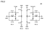
- FIG. 2 is an equivalent circuit diagram of the filter device 100.
- the filter device 100 includes an input terminal T1, an output terminal T2, a ground terminal GND, and resonators RC11 to RC14.
- Each of the resonators RC11 to RC14 is an LC resonator including an inductor and a capacitor.
- the resonator RC11 is connected to the input terminal T1 and the resonator RC12 is connected to the output terminal T2.
- the resonators RC13 and RC14 are arranged between the resonator RC11 and the resonator RC12.
- the resonator RC11 includes inductors L111, L112, L113 and capacitors C111, C112.
- the inductors L111 and L112 and the capacitor C112 are connected in series between the input terminal T1 and the ground terminal GND in this order.
- the inductor L113 is connected between the connection node of the inductor L111 and the inductor L112 and the ground terminal GND.
- the capacitor C111 is connected between the input terminal T1 and the ground terminal GND.
- the resonator RC12 includes inductors L121, L122, L123 and capacitors C121, C122.
- the inductors L121 and L122 and the capacitor C122 are connected in series between the output terminal T2 and the ground terminal GND in this order.
- the inductor L123 is connected between the connection node of the inductor L121 and the inductor L122 and the ground terminal GND.
- the capacitor C121 is connected between the output terminal T2 and the ground terminal GND.
- the resonator RC13 includes an inductor L131 and capacitors C131 and C132. One end of the inductor L131 is connected to the ground terminal GND via the capacitor C131. The other end of the inductor L131 is connected to the ground terminal GND via the capacitor C132. The inductor L131 is DC-insulated from the ground terminal GND by the capacitors C131 and C132.
- the resonator RC14 includes an inductor L141 and capacitors C141 and C142. One end of the inductor L141 is connected to the ground terminal GND via the capacitor C141. The other end of the inductor L141 is connected to the ground terminal GND via the capacitor C142. The inductor L141 is DC-insulated from the ground terminal GND by the capacitors C141 and C142.
- Each resonator is coupled by electromagnetic field coupling.
- the filter device 100 has a configuration in which four-stage resonators that are electromagnetically coupled to each other are arranged between the input terminal T1 and the output terminal T2.
- the high frequency signal input to the input terminal T1 is transmitted by the electromagnetic field coupling of the resonators RC11 to RC14, and is output from the output terminal T2.
- the filter device 100 functions as a bandpass filter for passing a signal in a desired frequency band by adjusting the resonance frequency of each resonator.
- FIG. 3 is an external perspective view of the filter device 100
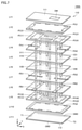
- FIG. 4 is an exploded perspective view showing an example of the laminated structure of the filter device 100.
- the filter device 100 includes a rectangular parallelepiped or substantially rectangular parallelepiped dielectric substrate 110 formed by stacking a plurality of dielectric layers LY1 to LY11 along a predetermined direction. .. In the dielectric substrate 110, the direction in which a plurality of dielectric layers LY1 to LY11 are stacked is defined as the stacking direction.
- Each dielectric layer of the dielectric substrate 110 is formed of, for example, a ceramic such as low temperature co-fired ceramics (LTCC: Low Temperature Co-fired Ceramics) or a resin.
- a plurality of electrodes provided in each dielectric layer and a plurality of vias provided between the dielectric layers form an inductor and a capacitor for forming an LC resonance circuit.
- via means a conductor provided in a dielectric layer for connecting electrodes provided in different dielectric layers. Vias are formed, for example, by conductive paste, plating, and / or metal pins.
- the stacking direction of the dielectric substrate 110 is defined as the "Z-axis direction", and the direction perpendicular to the Z-axis direction and along the long side of the dielectric substrate 110 is defined as the "X-axis direction”.
- the direction along the short side of the dielectric substrate 110 is defined as the "Y-axis direction”.
- the positive direction of the Z axis in each figure may be referred to as an upper side, and the negative direction may be referred to as a lower side.
- a directional mark DM for specifying the direction of the filter device 100 is arranged on the upper surface 111 (dielectric layer LY1) of the dielectric substrate 110.
- An input terminal T1, an output terminal T2, and a ground terminal GND are arranged on the lower surface 112 (dielectric layer LY11) of the dielectric substrate 110.
- Each of the input terminal T1, the output terminal T2, and the two ground terminals GND is a flat plate-shaped electrode.
- the input terminal T1 is arranged so as to be in contact with one side of the dielectric layer LY11 along the Y axis.
- the input terminal T1 is connected to a side electrode 121 provided on the side surface 114 of the dielectric substrate 110.
- the output terminal T2 is arranged so as to be in contact with the other side of the dielectric layer LY11 along the Y axis.
- the output terminal T2 is connected to a side electrode 120 provided on the side surface 113 of the dielectric substrate 110.
- the two ground terminals GND are arranged so as to be in contact with each of the two sides of the dielectric layer LY11 along the X axis.
- One ground terminal GND is connected to a side electrode 122 provided on the side surface 115 of the dielectric substrate 110.
- the other ground terminal GND is connected to a side electrode 123 provided on the side surface 116 of the dielectric substrate 110.
- a flat plate-shaped ground electrode PG1 is arranged on the dielectric layer LY2 of the dielectric substrate 110. Further, a flat plate-shaped ground electrode PG2 is arranged on the dielectric layer LY10 of the dielectric substrate 110.
- the ground electrodes PG1 and PG2 are connected to the ground terminal GND arranged in the dielectric layer LY11 by the side electrodes 122 and 123.
- the filter device 100 is connected to an external device by using an input terminal T1, an output terminal T2 and a ground terminal GND arranged on the lower surface 112 of the dielectric substrate 110, or side electrodes 120 to 123.
- the filter device 100 includes a four-stage LC resonator. More specifically, the filter device 100 includes a resonator RC11, a resonator RC12, a resonator RC13, and a resonator RC14.
- the resonator RC11 includes vias V10 and V11 and capacitor electrodes PC11 and PC12.
- the resonator RC12 includes vias V20 and V21 and capacitor electrodes PC21 and PC22.
- the resonator RC13 includes a via V30 and capacitor electrodes PC31 and PC32.
- the resonator RC14 includes a via V40 and capacitor electrodes PC41 and PC42.
- the capacitor electrode PC 11 is a rectangular flat plate electrode and is provided on the dielectric layer LY3. When viewed in a plan view from the normal direction (Z-axis direction) of the dielectric substrate 110, a part of the capacitor electrode PC 11 overlaps with the ground electrode PG1 provided in the dielectric layer LY2.
- the capacitor C111 of FIG. 2 is configured by the capacitor electrode PC11 and the ground electrode PG1.
- the capacitor electrode PC12 is a rectangular flat plate electrode and is provided on the dielectric layer LY9. When viewed in a plan view from the normal direction of the dielectric substrate 110, a part of the capacitor electrode PC 12 overlaps with the ground electrode PG2 provided in the dielectric layer LY10.
- the capacitor C112 of FIG. 2 is configured by the capacitor electrode PC12 and the ground electrode PG2.
- the capacitor electrode PC 11 is connected to the capacitor electrode PC 12 by vias V10 and V11.
- the via V10 is connected to the connection electrode PA1 provided on the dielectric layer LY4.
- the connection electrode PA1 is connected to the input terminal T1 via the side electrode 121.
- the vias V10 and V11 are also connected to the shunt electrode PB1 provided in the dielectric layer LY8.
- the shunt electrode PB1 is a strip-shaped flat plate electrode having a first end and a second end, the first end is connected to the side electrode 122, and the second end is connected to the side electrode 123. ing. That is, the shunt electrode PB1 is an electrode connected between the intermediate portion of the vias V10 and V11 and the ground terminal GND.
- the shunt electrode PB1 constitutes the inductor L113 in FIG. The inductance of the inductor L113 can be adjusted by changing the dimensions of the shunt electrode PB1 in the X-axis direction.
- the inductor L111 in FIG. 2 is configured by the portions of the vias V10 and V11 between the capacitor electrode PC11 and the shunt electrode PB1. Further, the inductor L112 of FIG. 2 is configured by the portions of the vias V10 and V11 between the capacitor electrode PC12 and the shunt electrode PB1. By changing the dielectric layer provided with the shunt electrode PB1, the magnitude (ratio) of the inductance of the inductors L111 and L112 can be adjusted.
- the capacitor electrode PC21 is a rectangular flat plate electrode and is provided on the dielectric layer LY3. When viewed in a plan view from the normal direction of the dielectric substrate 110, a part of the capacitor electrode PC 21 overlaps with the ground electrode PG1 provided in the dielectric layer LY2.
- the capacitor C121 of FIG. 2 is configured by the capacitor electrode PC21 and the ground electrode PG1.
- the capacitor electrode PC 22 is a rectangular flat plate electrode and is provided on the dielectric layer LY9. When viewed in a plan view from the normal direction of the dielectric substrate 110, a part of the capacitor electrode PC 22 overlaps with the ground electrode PG2 provided in the dielectric layer LY10.
- the capacitor C122 of FIG. 2 is configured by the capacitor electrode PC22 and the ground electrode PG2.
- the capacitor electrode PC21 is connected to the capacitor electrode PC22 by vias V20 and V21.
- the via V20 is connected to the connection electrode PA2 provided on the dielectric layer LY4.
- the connection electrode PA2 is connected to the output terminal T2 via the side electrode 120.
- the vias V20 and V21 are also connected to the shunt electrode PB2 provided in the dielectric layer LY8.
- the shunt electrode PB2 is a strip-shaped flat plate electrode having a first end and a second end, the first end is connected to the side electrode 122, and the second end is connected to the side electrode 123. ing. That is, the shunt electrode PB2 is an electrode connected between the intermediate portion of the vias V20 and V21 and the ground terminal GND.
- the shunt electrode PB2 constitutes the inductor L123 in FIG. The inductance of the inductor L123 can be adjusted by changing the dimensions of the shunt electrode PB2 in the X-axis direction.
- the inductor L121 of FIG. 2 is configured by the portions of the vias V20 and V21 between the capacitor electrode PC21 and the shunt electrode PB2. Further, the inductor L122 of FIG. 2 is configured by the portions of the vias V20 and V21 between the capacitor electrode PC22 and the shunt electrode PB2. By changing the dielectric layer provided with the shunt electrode PB2, the magnitude (ratio) of the inductance of the inductors L121 and L122 can be adjusted.
- the capacitor electrode PC31 is a rectangular flat plate electrode and is provided on the dielectric layer LY3. When viewed in a plan view from the normal direction of the dielectric substrate 110, a part of the capacitor electrode PC 31 overlaps with the ground electrode PG1 provided on the dielectric layer LY2.
- the capacitor C131 of FIG. 2 is configured by the capacitor electrode PC31 and the ground electrode PG1.
- the capacitor electrode PC 32 is a rectangular flat plate electrode, and is provided on the dielectric layer LY9. When viewed in a plan view from the normal direction of the dielectric substrate 110, a part of the capacitor electrode PC 32 overlaps with the ground electrode PG2 provided in the dielectric layer LY10.
- the capacitor C132 of FIG. 2 is configured by the capacitor electrode PC32 and the ground electrode PG2.
- the capacitor electrode PC 31 is connected to the capacitor electrode PC 32 by a via V30.
- the via V30 constitutes the inductor L131 of FIG.
- the capacitor electrode PC41 is a rectangular flat plate electrode and is provided on the dielectric layer LY3. When viewed in a plan view from the normal direction of the dielectric substrate 110, a part of the capacitor electrode PC 41 overlaps with the ground electrode PG1 provided on the dielectric layer LY2.
- the capacitor C141 of FIG. 2 is configured by the capacitor electrode PC41 and the ground electrode PG1.
- the capacitor electrode PC 42 is a rectangular flat plate electrode and is provided on the dielectric layer LY9. When viewed in a plan view from the normal direction of the dielectric substrate 110, a part of the capacitor electrode PC 42 overlaps with the ground electrode PG2 provided in the dielectric layer LY10.
- the capacitor C142 of FIG. 2 is configured by the capacitor electrode PC42 and the ground electrode PG2.
- the capacitor electrode PC 41 is connected to the capacitor electrode PC 42 by a via V40.
- the via V40 constitutes the inductor L141 of FIG.
- the capacitor electrode PC11 of the resonator RC11 is arranged close to the side surface 114, and the capacitor electrode PC21 of the resonator RC12 is arranged close to the side surface 113. Further, the capacitor electrode PC31 of the resonator RC13 and the capacitor electrode PC41 of the resonator RC14 are arranged in parallel along the X axis between the capacitor electrode PC11 and the capacitor electrode PC21 in the dielectric layer LY3. Further, the capacitor electrodes PC12, PC22, PC32, and PC42 in the dielectric layer LY9 have the same arrangement. The arrangement of the resonator shown in FIG.
- resonator RC13 is arranged between the resonator RC11 and the resonator RC12
- the resonator RC14 is arranged between the resonator RC12 and the resonator RC13. It may be configured as such.
- the resonator RC11 and the resonator RC12 are loop-type resonators in which two capacitor electrodes are connected by two vias.
- the resistance component of the path between the capacitor electrodes can be reduced, and the current flowing through each via can be reduced. Therefore, Q is compared with the case where two capacitor electrodes are connected by a single via. The value can be improved. Further, since the air core diameter of the coil can be increased by forming the loop shape, the Q value can also be improved.
- the capacitor electrodes may be connected by using a plurality of vias.
- the filter device using a plurality of resonators including a resonator that is DC-insulated from the ground terminal, the coupling between the resonators is capacitively coupled from the magnetic coupling in terms of transmission characteristics. Since the impedance on the ground side can be made capacitive on the high frequency side, in addition to improving the attenuation characteristics on the high frequency side, an attenuation pole is generated on the high frequency side of the passing band. do.
- the resonator RC11 connected to the input terminal T1 and the resonator RC12 connected to the output terminal T2 include the shunt electrodes PB1 and PB2, respectively. Attenuation poles are generated on the low frequency side of the pass band due to the reduction of the impedance on the low frequency side of the resonators RC11 and RC12 by the shunt electrode and the inductance connected in series with the capacitors C112 and C122.
- the shunt electrode may be included in only one of the input side resonator RC11 and the output side resonator RC12, but if the symmetry of the input / output impedance characteristics of the filter is required, the shunt electrode may be included in only one of them. It is preferable that it is contained in both the resonators RC11 and RC12.
- FIG. 5 is a diagram for explaining the passing characteristics of the filter device 100.
- the upper row shows the passing characteristics of the filter device 100
- the lower row shows the passing characteristics of the filter device of the comparative example.
- the filter device of the comparative example is a bandpass filter having a configuration in which the shunt electrodes PB1 and PB2 are removed from the filter device 100.
- the solid lines LN10 and LN15 indicate the insertion loss
- the broken lines LN11 and LN16 indicate the reflection loss.
- the attenuation pole is generated on the higher frequency side than the pass band, but the pass band. No attenuation electrode is generated on the lower frequency side.
- the filter device 100 of the first embodiment attenuation poles are generated on both the high frequency side and the low frequency side of the pass band.
- a resonator that is electrically isolated is used, and the resonator connected to the input / output terminal includes a shunt electrode to form a band. Attenuation poles are generated on both the high frequency side and the low frequency side of the pass band of the pass filter. This makes it possible to improve the attenuation characteristics in the non-passband band of the filter device.
- the capacitor electrodes PC11, PC21, PC31, and PC41 which are the first capacitor electrodes
- the capacitor electrodes PC12, PC22, PC32, and PC42 which are the second capacitor electrodes
- the capacitors C112, C122, C132, and C142 configured have a large capacitance, and the ground electrode PG2 is arranged closer to the ground terminal GND than the ground electrode PG1.
- the dielectric constant of the dielectric layer LY9 between the capacitor electrodes PC12, PC22, PC32, PC42, which are the second capacitor electrodes, and the ground electrode PG2 is set to the capacitor electrodes PC11, PC21, PC31, which are the first capacitor electrodes.
- the distance between the second capacitor electrodes PC12, PC22, PC32, PC42 and the ground electrode PG2 is set between the first capacitor electrodes PC11, PC21, PC31, PC41 and the ground electrode PG1. Make it shorter than the interval between.
- the filter device may be configured to include three resonators excluding the resonator RC14.
- the "resonator RC11”, “resonator RC12”, “resonator RC13” and “resonator RC14" in the first embodiment are the “first LC resonator”, “second LC resonator”, “second LC resonator” in the present disclosure. It corresponds to the “third LC resonator” and the “fourth LC resonator”, respectively.
- the “ground electrode PG1” and “ground electrode PG2" in the first embodiment correspond to the “first ground electrode” and the “second ground electrode” in the present disclosure, respectively.
- “via V10, V11, V20, V21, V30, V40” corresponds to the "first via” in the present disclosure.
- the "capacitor electrodes PC11, PC21, PC31, PC41” correspond to the “first capacitor electrode” in the present disclosure.
- the “capacitor electrodes PC12, PC22, PC32, PC42” correspond to the “second capacitor electrode” in the present disclosure.
- the “branch electrode PB1" and “branch electrode PB2" in the first embodiment correspond to the “first branch electrode” and the “second branch electrode” in the disclosure, respectively.
- Each of the “side electrodes 122 and 123" in the first embodiment corresponds to the “first side electrode” in the present disclosure.
- the “side electrode 121" and “side electrode 120" in the first embodiment correspond to the “second side electrode” and the “third side electrode” in the present disclosure, respectively.
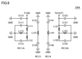
- FIG. 6 is an equivalent circuit diagram of the filter device 100A of the second embodiment.
- the filter device 100A has a configuration in which a capacitor for impedance adjustment is added to the resonator RC11 on the input side and the resonator RC12 on the output side in the filter device 100 of the first embodiment described with reference to FIG.
- FIG. 6 and FIG. 7 described later the description of the elements overlapping with FIGS. 2 and 4 in the first embodiment will not be repeated.
- the filter device 100A has an input terminal T1, an output terminal T2, a ground terminal GND, and resonators RC11A, RC12A, RC13, and RC14, similarly to the filter device 100 of the first embodiment. Be prepared.
- the resonator RC11A connected to the input terminal T1 has a configuration in which a capacitor C113 connected between the input terminal T1 and the ground terminal GND is added to the configuration of the resonator RC11 in the filter device 100.
- the resonator RC12A connected to the output terminal T2 has a configuration in which a capacitor C123 connected between the output terminal T2 and the ground terminal GND is added to the configuration of the resonator RC12 in the filter device 100. is doing.
- the resonators RC13 and RC14 have the same configuration as the resonators RC13 and RC14 in the filter device 100.
- the impedance with the equipment can be adjusted. Can be done. Thereby, the reflection loss can be reduced.
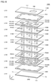
- FIG. 7 is an exploded perspective view showing an example of the laminated structure of the filter device 100A of FIG.
- the capacitor electrodes PD1 and PD2 provided in the dielectric layer LY7 are added.
- the capacitor electrode PD1 is a strip-shaped flat plate electrode extending along the X-axis, and is partially the shunt electrode PB1 arranged in the dielectric layer LY8 when viewed in a plan view from the normal direction of the dielectric substrate 110. It overlaps with.
- One end of the capacitor electrode PD1 is connected to the input terminal T1 and the connection electrode PA1 via the side electrode 121 arranged on the side surface 114 of the dielectric substrate 110.
- the capacitor C113 in FIG. 6 is configured by the capacitor electrode PD1 and the shunt electrode PB1.
- the capacitance of the capacitor C113 changes. Thereby, the input impedance of the filter device 100A can be adjusted.
- the capacitor electrode PD2 is a strip-shaped flat plate electrode extending along the X-axis, and is partially the shunt electrode PB2 arranged in the dielectric layer LY8 when viewed in a plan view from the normal direction of the dielectric substrate 110. It overlaps with. Further, one end of the capacitor electrode PD2 is connected to the output terminal T2 and the connection electrode PA2 via the side electrode 120 arranged on the side surface 113 of the dielectric substrate 110.
- the capacitor C123 in FIG. 6 is configured by the capacitor electrode PD2 and the shunt electrode PB2.
- the width of the capacitor electrode PD2 to adjust the area overlapping with the shunt electrode PB2
- the capacitance of the capacitor C123 changes. Thereby, the output impedance of the filter device 100A can be adjusted.
- FIG. 8 is a diagram showing the passing characteristics of the filter device 100A of FIG.
- the solid line LN20 shows the insertion loss
- the broken line LN21 shows the reflection loss.
- the resonator RC11A connected to the input terminal T1 and the resonator RC12A connected to the output terminal T2 are divided. Since the road electrodes PB1 and PB2 are arranged respectively, attenuation poles are generated on both the high frequency side and the low frequency side of the pass band.
- the optimum input / output impedance can be matched by the capacitor electrodes PD1 and PD2 arranged in the resonators RC11A and RC12A, respectively.
- the reflection loss in the pass band is reduced as a whole as compared with the filter device 100 shown in FIG.
- the shunt electrode and the capacitor electrode for impedance adjustment for the resonator connected to the input / output terminal, the attenuation characteristic in the non-passband of the filter device is improved and the reflection in the passband is improved.
- the loss can be reduced.
- the "resonator RC11A” and the “resonator RC12A” correspond to the “first LC resonator” and the “second LC resonator” in the present disclosure, respectively.
- the “capacitor electrode PD1” and the “capacitor electrode PD2" in the second embodiment correspond to the “third capacitor electrode” and the “fourth capacitor electrode” in the present disclosure, respectively.
- FIG. 9 is an equivalent circuit diagram of the filter device 100B of the third embodiment.
- the filter device 100B includes an input terminal T1, an output terminal T2, a ground terminal GND, and resonators RC21 to RC25.
- Each of the resonators RC21 to RC25 is an LC resonator including an inductor and a capacitor.
- the resonator RC21 is connected to the input terminal T1, and the resonator RC22 is connected to the output terminal T2.
- the resonators RC23 to RC25 are arranged in this order between the resonator RC21 and the resonator RC22.
- the resonator RC21 includes inductors L211, L212, L213 and capacitors C211 and C212.
- the inductors L211 and L212 and the capacitor C212 are connected in series between the input terminal T1 and the ground terminal GND in this order.
- the inductor L213 is connected between the connection node of the inductor L211 and the inductor L212 and the ground terminal GND.
- the capacitor C211 is connected between the input terminal T1 and the ground terminal GND.
- the resonator RC22 includes inductors L221, L222, L223 and capacitors C221 and C222.
- the inductors L221 and L222 and the capacitor C222 are connected in series between the output terminal T2 and the ground terminal GND in this order.
- the inductor L223 is connected between the connection node of the inductor L221 and the inductor L222 and the ground terminal GND.
- the capacitor C221 is connected between the output terminal T2 and the ground terminal GND.
- the resonator RC23 includes inductors L231 and L232 and capacitors C231 and C232. One end of the inductor L231 is connected to the ground terminal GND via the capacitor C231. The other end of the inductor L231 is connected to the ground terminal GND via the capacitor C232. The inductor L232 is connected in parallel to the inductor L231. The inductors L231 and L232 are DC-isolated from the ground terminal GND by the capacitors C231 and C232.
- the resonator RC24 includes inductors L241 and L242 and capacitors C241 and C242. One end of the inductor L241 is connected to the ground terminal GND via the capacitor C241. The other end of the inductor L241 is connected to the ground terminal GND via the capacitor C242. The inductor L242 is connected in parallel to the inductor L241. The inductors L241 and L242 are DC-isolated from the ground terminal GND by the capacitors C241 and C242.
- the resonator RC25 includes an inductor L251 and capacitors C251 and C252. One end of the inductor L251 is connected to the ground terminal GND via the capacitor C251. The other end of the inductor L251 is connected to the ground terminal GND via the capacitor C252. The inductor L251 is DC-insulated from the ground terminal GND by the capacitors C251 and C252.
- Each resonator is coupled by electromagnetic field coupling.
- the filter device 100B has a configuration in which five-stage resonators that are electromagnetically coupled to each other are arranged between the input terminal T1 and the output terminal T2.
- the high frequency signal input to the input terminal T1 is transmitted by the electromagnetic field coupling of the resonators RC21 to RC25, and is output from the output terminal T2.
- the filter device 100B functions as a bandpass filter for passing a signal in a desired frequency band by adjusting the resonance frequency of each resonator.
- FIG. 10 is an exploded perspective view showing an example of the laminated structure of the filter device 100B of FIG.
- the filter device 100B includes a rectangular parallelepiped or substantially rectangular parallelepiped dielectric substrate 110B formed by stacking a plurality of dielectric layers LY21 to LY31 along a predetermined direction.
- Each dielectric layer of the dielectric substrate 110B is formed of a ceramic such as LTCC or a resin, similarly to the dielectric substrate 110 of the filter device 100.
- a directional mark DM for specifying the direction of the filter device 100B is arranged on the upper surface 111 (dielectric layer LY21) of the dielectric substrate 110B.
- An input terminal T1, an output terminal T2, and a ground terminal GND are arranged on the lower surface 112 (dielectric layer LY31) of the dielectric substrate 110B.
- the input terminal T1, the output terminal T2, and the ground terminal GND are connected to a side electrode provided on the side surface of the dielectric substrate 110B, similarly to the filter device 100.
- a flat plate-shaped ground electrode PG1 is arranged on the dielectric layer LY22 of the dielectric substrate 110B. Further, a flat plate-shaped ground electrode PG2 is arranged on the dielectric layer LY30 of the dielectric substrate 110B. The ground electrodes PG1 and PG2 are connected to the ground terminal GND arranged in the dielectric layer LY31 by the side electrodes.
- the filter device 100B includes a five-stage LC resonator. More specifically, the filter device 100B includes a resonator RC21, a resonator RC22, a resonator RC23, a resonator RC24, and a resonator RC25.
- the resonator RC21 includes vias V10B and V15B and capacitor electrodes PC11B and PC12B.
- the resonator RC22 includes vias V20 and V25B and capacitor electrodes PC21B and PC22B.
- the resonator RC23 includes vias V30B and V31B and capacitor electrodes PC31B and PC32B.
- the resonator RC24 includes vias V40B and V41B and capacitor electrodes PC41B and PC42B.
- the resonator RC25 includes a via V50B and capacitor electrodes PC51B and PC52B.
- the capacitor electrode PC11B is a rectangular flat plate electrode and is provided on the dielectric layer LY23. When viewed in a plan view from the normal direction of the dielectric substrate 110B, a part of the capacitor electrode PC 11B overlaps with the ground electrode PG1 provided on the dielectric layer LY22.
- the capacitor electrode PC11B and the ground electrode PG1 constitute the capacitor C211 in FIG. 9.
- the capacitor electrode PC12B is a rectangular flat plate electrode and is provided on the dielectric layer LY29. When viewed in a plan view from the normal direction of the dielectric substrate 110B, a part of the capacitor electrode PC12B overlaps with the ground electrode PG2 provided in the dielectric layer LY30.
- the capacitor C212 of FIG. 9 is configured by the capacitor electrode PC12B and the ground electrode PG2.
- the capacitor electrode PC11B is connected to the capacitor electrode PC12B by a via V10B.
- the via V10B is connected to the connection electrode PA1B provided on the dielectric layer LY24.
- the connection electrode PA1B is connected to the input terminal T1 via the side electrode 121.
- the via V10B is also connected to the shunt electrode PB1B provided on the dielectric layer LY28.
- the shunt electrode PB1B is a strip-shaped flat plate electrode having a first end and a second end, and the first end and the second end are connected to the ground terminal GND via the side electrodes 122 and 123, respectively. ing. That is, the shunt electrode PB1B is an electrode connected between the intermediate portion of the via V10B and the ground terminal GND.
- the shunt electrode PB1B constitutes the inductor L213 in FIG. The inductance of the inductor L213 can be adjusted by changing the dimensions of the shunt electrode PB1B in the X-axis direction.
- the shunt electrode PB1B and the capacitor electrode PC12B are connected by a via V15B in addition to the via V10B.
- the portion of the via V10B between the capacitor electrode PC11B and the shunt electrode PB1B constitutes the inductor L211 of FIG.
- the inductor L212 of FIG. 9 is configured by the portion of the via V10B and the via V15B between the capacitor electrode PC12B and the shunt electrode PB1B.
- the capacitor electrode PC21B is a rectangular flat plate electrode and is provided on the dielectric layer LY23. When viewed in a plan view from the normal direction of the dielectric substrate 110B, a part of the capacitor electrode PC21B overlaps with the ground electrode PG1 provided on the dielectric layer LY22.
- the capacitor C221 of FIG. 9 is configured by the capacitor electrode PC21B and the ground electrode PG1.
- the capacitor electrode PC22B is a rectangular flat plate electrode and is provided on the dielectric layer LY29. When viewed in a plan view from the normal direction of the dielectric substrate 110B, a part of the capacitor electrode PC22B overlaps with the ground electrode PG2 provided in the dielectric layer LY30.
- the capacitor C222 of FIG. 9 is configured by the capacitor electrode PC22B and the ground electrode PG2.
- the capacitor electrode PC21B is connected to the capacitor electrode PC22B by a via V20B.
- the via V20B is connected to the connection electrode PA2B provided on the dielectric layer LY24.
- the connection electrode PA2B is connected to the output terminal T2 via the side electrode 120.
- the via V20B is also connected to the shunt electrode PB2B provided on the dielectric layer LY28.
- the shunt electrode PB2B is a strip-shaped flat plate electrode having a first end portion and a second end portion, and the first end portion and the second end portion are connected to the ground terminal GND via a side electrode. That is, the shunt electrode PB2B is an electrode connected between the intermediate portion of the via V20B and the ground terminal GND.
- the shunt electrode PB2B constitutes the inductor L223 in FIG. The inductance of the inductor L223 can be adjusted by changing the dimensions of the shunt electrode PB2B in the X-axis direction.
- the shunt electrode PB2B and the capacitor electrode PC22B are connected by a via V25B in addition to the via V20B.
- the portion of the via V20B between the capacitor electrode PC21B and the shunt electrode PB2B constitutes the inductor L221 of FIG.
- the inductor L222 of FIG. 9 is configured by the portion of the via V20B between the capacitor electrode PC22B and the shunt electrode PB2B and the via V25B.
- the capacitor electrode PC31B is a rectangular flat plate electrode and is provided on the dielectric layer LY23. When viewed in a plan view from the normal direction of the dielectric substrate 110B, a part of the capacitor electrode PC31B overlaps with the ground electrode PG1 provided on the dielectric layer LY22.
- the capacitor C231 of FIG. 9 is configured by the capacitor electrode PC31B and the ground electrode PG1.
- the capacitor electrode PC32B is a rectangular flat plate electrode and is provided on the dielectric layer LY29. When viewed in a plan view from the normal direction of the dielectric substrate 110B, a part of the capacitor electrode PC 32B overlaps with the ground electrode PG2 provided in the dielectric layer LY30.
- the capacitor electrode PC32B is connected to the capacitor electrode PC32B by vias V30B and V31B. Vias V30B and V31B constitute the inductors L231 and L232 of FIG.
- the capacitor electrode PC41B is a rectangular flat plate electrode and is provided on the dielectric layer LY23. When viewed in a plan view from the normal direction of the dielectric substrate 110B, a part of the capacitor electrode PC41B overlaps with the ground electrode PG1 provided on the dielectric layer LY22.
- the capacitor C241 of FIG. 9 is configured by the capacitor electrode PC41B and the ground electrode PG1.
- the capacitor electrode PC42B is a rectangular flat plate electrode and is provided on the dielectric layer LY29. When viewed in a plan view from the normal direction of the dielectric substrate 110B, a part of the capacitor electrode PC 42B overlaps with the ground electrode PG2 provided in the dielectric layer LY30.
- the capacitor electrode PC41B is connected to the capacitor electrode PC42B by vias V40B and V41B. Vias V40B and V41B constitute the inductors L241 and L242 of FIG.
- the capacitor electrode PC51B is a rectangular flat plate electrode and is provided on the dielectric layer LY23. When viewed in a plan view from the normal direction of the dielectric substrate 110B, a part of the capacitor electrode PC51B overlaps with the ground electrode PG1 provided on the dielectric layer LY22.
- the capacitor C251 of FIG. 9 is configured by the capacitor electrode PC51B and the ground electrode PG1.
- the capacitor electrode PC 52B is a rectangular flat plate electrode and is provided on the dielectric layer LY29. When viewed in a plan view from the normal direction of the dielectric substrate 110B, a part of the capacitor electrode PC 52B overlaps with the ground electrode PG2 provided in the dielectric layer LY30.
- the capacitor C252 of FIG. 9 is configured by the capacitor electrode PC52B and the ground electrode PG2.
- the capacitor electrode PC51B is connected to the capacitor electrode PC52B by a via V50B.
- the via V50B constitutes the inductor L251 of FIG.
- the capacitor electrodes in the dielectric layer LY23 of the dielectric substrate 110B are the capacitor electrode PC11B, the capacitor electrode PC31B, the capacitor electrode PC51B, the capacitor electrode PC41B, and the capacitor electrode PC21B from the side surface 114 to the side surface 113 of the dielectric substrate 110B. They are arranged in the order of. Similarly, the capacitor electrodes in the dielectric layer LY29 are arranged in the order of the capacitor electrode PC12B, the capacitor electrode PC32B, the capacitor electrode PC52B, the capacitor electrode PC42B, and the capacitor electrode PC22B from the side surface 114 to the side surface 113 of the dielectric substrate 110B. ing.
- the resonators RC23 and RC24 are loop type resonators in which two capacitor electrodes are connected by two vias.
- the resistance component of the path between the capacitor electrodes can be reduced and the current flowing through each via can be reduced. Therefore, when the two capacitor electrodes are connected by a single via.
- the Q value can be improved as compared with. Further, since the air core diameter of the coil can be increased by forming the loop shape, the Q value can also be improved.
- the resonator RC25 may be a loop type resonator.
- FIG. 11 is a diagram showing the passing characteristics of the filter device 100B of FIG.
- the solid line LN30 shows the insertion loss
- the broken line LN31 shows the reflection loss.
- the attenuation amount of the attenuation pole on the low frequency side near the pass band is about 43 dB, which is higher than the attenuation amount (about 34 dB) of the four-stage filter device 100 in the first embodiment shown in FIG. Can also achieve a large amount of attenuation.
- the number of stages of the resonator may be six or more. However, as the number of stages of the resonator increases, the passband characteristic tends to become a wideband characteristic. Therefore, the number of stages of the resonator is determined in consideration of the balance between the target attenuation amount and the pass bandwidth.
- a bandpass is obtained by using a DC-insulated resonator and including a shunt electrode in the resonator connected to the input / output terminal. Attenuation poles are generated on both the high frequency side and the low frequency side of the pass band of the filter. This makes it possible to improve the attenuation characteristics in the non-passband band of the filter device.
- the "resonator RC21”, “resonator RC22”, “resonator RC23”, “resonator RC24” and “resonator RC25” are the “first LC resonator” and “resonator RC25” in the present disclosure. It corresponds to the “second LC resonator”, “third LC resonator”, “fourth LC resonator” and “fifth LC resonator”, respectively.
- “via V10B, V20B, V30B, V31B, V40B, V41B, V50B” corresponds to the "first via” in the present disclosure.
- the “via V15B” and “via 25B” in the fourth embodiment correspond to the "second via” and the "third via” of the present disclosure, respectively.
- the “capacitor electrodes PC11B, PC21B, PC31B, PC41B, PC51B” correspond to the "first capacitor electrode” in the present disclosure.
- the “capacitor electrodes PC12B, PC22B, PC32B, PC42B, PC52B” correspond to the "second capacitor electrode” in the present disclosure.
- the “branch electrode PB1B” and “branch electrode PB2B” in the fourth embodiment correspond to the "first branch electrode” and the "second branch electrode” in the disclosure, respectively.
- connection between the ground electrodes PG1 and PG2 and the ground terminal GND, the connection between the connection electrode PA1 and the input terminal T1, and the connection between the connection electrode PA2 and the output terminal T2 are made of a dielectric substrate.
- the configuration performed using the side electrode formed on the side surface of the 110 has been described.
- FIG. 12 is an exploded perspective view showing an example of the laminated structure of the filter device 100C of the fourth embodiment.
- FIG. 12 shows a configuration in which vias VT1, VT2, VG1, and VG2 are added to the configuration of the filter device 100A described in the second embodiment.
- the side electrodes 120 to 123 in FIG. 2 are not arranged. It should be noted that the description of the elements overlapping with FIG. 7 in FIG. 12 is not repeated.
- vias VT1, VT2, VG1 and VG2 are provided from the dielectric layer LY2 to the dielectric layer LY11 along each side surface of the dielectric substrate 110. More specifically, the via VT1 is provided from the dielectric layer LY2 to the dielectric layer LY11 along the side surface 114 of the dielectric substrate 110.
- a connection electrode PA1, a capacitor electrode PD1, and an input terminal T1 are connected to the via VT1.
- the via VT2 is provided from the dielectric layer LY2 to the dielectric layer LY11 along the side surface 113 of the dielectric substrate 110.
- a connection electrode PA2, a capacitor electrode PD2, and an output terminal T2 are connected to the via VT2.
- a plurality of vias VG1 are provided from the dielectric layer LY2 to the dielectric layer LY11 along the side surface 115 of the dielectric substrate 110, and the dielectric layer is provided from the dielectric layer LY2 along the side surface 116 of the dielectric substrate 110.
- a plurality of vias VG2 are provided over LY11.
- a ground electrode PG1, a ground electrode PG2, and a ground terminal GND are connected to the vias VG1 and VG2.
- the connection between the filter device 100C and the external device is performed by the input terminal T1, the output terminal T2, and the ground terminal GND arranged on the lower surface 112. That is, the filter device 100C has an LGA (Land Grid Array) terminal structure. With such a configuration, it is possible to reduce the mounting area because the connection using the side electrodes is not required.
- LGA Land Grid Array
- via VG1 and VG2 in the fourth embodiment correspond to the “fourth via” in the present disclosure.
- the "via VT1" and “via VT2" in the fourth embodiment correspond to the "fifth via” and the “sixth via” in the present disclosure, respectively.
- Equipment 110, 110B dielectric substrate, 111 upper surface, 112 lower surface, 113 to 116 side surfaces, 120 to 123 side electrodes, C111 to C113, C121 to C123, C131, C132, C141, C142, C211, C212, C221, C222 C231, C231, C241, C242, C251, C252 Capacitor, DM Directional Mark, GND Ground Terminal, L111 to L113, L121 to L123, L131, L141, L211 to L213, L221 to L223, L231, L231, L241, L242 L251 inductor, LY1 to LY11, LY21 to LY31 dielectric layer, PA1, PA1B, PA2, PA2B connection electrode, PB1, PB1B, PB2, PB2B branch electrode, PC11 to PC14, PC11B, PC12B, PC21, PC21B, PC22, PC22B , PC31, PC31B, PC32, PC32B, PC41, PC41B
Landscapes
- Engineering & Computer Science (AREA)
- Power Engineering (AREA)
- Microelectronics & Electronic Packaging (AREA)
- Manufacturing & Machinery (AREA)
- Physics & Mathematics (AREA)
- Electromagnetism (AREA)
- Control Of Motors That Do Not Use Commutators (AREA)
- Filters And Equalizers (AREA)
- Coils Or Transformers For Communication (AREA)
Priority Applications (3)
| Application Number | Priority Date | Filing Date | Title |
|---|---|---|---|
| CN202180054811.8A CN116076019B (zh) | 2020-09-15 | 2021-08-04 | 滤波器装置、及具备该滤波器装置的高频前端电路 |
| JP2022550405A JP7517442B2 (ja) | 2020-09-15 | 2021-08-04 | フィルタ装置およびそれを備えた高周波フロントエンド回路 |
| US18/105,298 US12301196B2 (en) | 2020-09-15 | 2023-02-03 | Filter device and radio-frequency front end circuit including the same |
Applications Claiming Priority (2)
| Application Number | Priority Date | Filing Date | Title |
|---|---|---|---|
| JP2020154409 | 2020-09-15 | ||
| JP2020-154409 | 2020-09-15 |
Related Child Applications (1)
| Application Number | Title | Priority Date | Filing Date |
|---|---|---|---|
| US18/105,298 Continuation US12301196B2 (en) | 2020-09-15 | 2023-02-03 | Filter device and radio-frequency front end circuit including the same |
Publications (1)
| Publication Number | Publication Date |
|---|---|
| WO2022059373A1 true WO2022059373A1 (ja) | 2022-03-24 |
Family
ID=80776831
Family Applications (1)
| Application Number | Title | Priority Date | Filing Date |
|---|---|---|---|
| PCT/JP2021/028945 Ceased WO2022059373A1 (ja) | 2020-09-15 | 2021-08-04 | フィルタ装置およびそれを備えた高周波フロントエンド回路 |
Country Status (4)
| Country | Link |
|---|---|
| US (1) | US12301196B2 (https=) |
| JP (1) | JP7517442B2 (https=) |
| CN (1) | CN116076019B (https=) |
| WO (1) | WO2022059373A1 (https=) |
Cited By (1)
| Publication number | Priority date | Publication date | Assignee | Title |
|---|---|---|---|---|
| JP2024023011A (ja) * | 2022-08-08 | 2024-02-21 | 株式会社村田製作所 | フィルタ装置およびそれを備えた高周波フロントエンド回路 |
Families Citing this family (1)
| Publication number | Priority date | Publication date | Assignee | Title |
|---|---|---|---|---|
| US12512815B2 (en) * | 2022-09-15 | 2025-12-30 | Murata Manufacturing Co., Ltd. | Filter device and high-frequency front-end circuit provided with the same |
Citations (4)
| Publication number | Priority date | Publication date | Assignee | Title |
|---|---|---|---|---|
| JP2009517920A (ja) * | 2005-11-28 | 2009-04-30 | Tdk株式会社 | 複数の減衰極を有するバンドパスフィルタ |
| JP2013128232A (ja) * | 2011-12-19 | 2013-06-27 | Murata Mfg Co Ltd | バンドパスフィルタ |
| WO2018034103A1 (ja) * | 2016-08-17 | 2018-02-22 | 株式会社村田製作所 | 積層型lcフィルタ |
| JP2019079865A (ja) * | 2017-10-20 | 2019-05-23 | 太陽誘電株式会社 | 電子部品 |
Family Cites Families (7)
| Publication number | Priority date | Publication date | Assignee | Title |
|---|---|---|---|---|
| US7312676B2 (en) * | 2005-07-01 | 2007-12-25 | Tdk Corporation | Multilayer band pass filter |
| TW200908430A (en) * | 2007-05-18 | 2009-02-16 | Murata Manufacturing Co | Stacked bandpass filter |
| KR101572534B1 (ko) * | 2009-06-18 | 2015-11-30 | 삼성전자주식회사 | Rf 프론트 앤드 모듈 및 이를 이용한 멀티밴드 통신 모듈 |
| CN103210585B (zh) * | 2010-11-16 | 2015-09-02 | 株式会社村田制作所 | 层叠带通滤波器 |
| JP6662150B2 (ja) * | 2016-03-31 | 2020-03-11 | 株式会社村田製作所 | ハイパスフィルタ |
| CN110024283B (zh) | 2016-12-02 | 2023-02-17 | 株式会社村田制作所 | Lc谐振器以及lc滤波器 |
| US10432237B2 (en) | 2017-10-20 | 2019-10-01 | Taiyo Yuden Co., Ltd. | Multiplexer |
-
2021
- 2021-08-04 JP JP2022550405A patent/JP7517442B2/ja active Active
- 2021-08-04 CN CN202180054811.8A patent/CN116076019B/zh active Active
- 2021-08-04 WO PCT/JP2021/028945 patent/WO2022059373A1/ja not_active Ceased
-
2023
- 2023-02-03 US US18/105,298 patent/US12301196B2/en active Active
Patent Citations (4)
| Publication number | Priority date | Publication date | Assignee | Title |
|---|---|---|---|---|
| JP2009517920A (ja) * | 2005-11-28 | 2009-04-30 | Tdk株式会社 | 複数の減衰極を有するバンドパスフィルタ |
| JP2013128232A (ja) * | 2011-12-19 | 2013-06-27 | Murata Mfg Co Ltd | バンドパスフィルタ |
| WO2018034103A1 (ja) * | 2016-08-17 | 2018-02-22 | 株式会社村田製作所 | 積層型lcフィルタ |
| JP2019079865A (ja) * | 2017-10-20 | 2019-05-23 | 太陽誘電株式会社 | 電子部品 |
Cited By (3)
| Publication number | Priority date | Publication date | Assignee | Title |
|---|---|---|---|---|
| JP2024023011A (ja) * | 2022-08-08 | 2024-02-21 | 株式会社村田製作所 | フィルタ装置およびそれを備えた高周波フロントエンド回路 |
| JP7732417B2 (ja) | 2022-08-08 | 2025-09-02 | 株式会社村田製作所 | フィルタ装置およびそれを備えた高周波フロントエンド回路 |
| US12407319B2 (en) | 2022-08-08 | 2025-09-02 | Murata Manufacturing Co., Ltd. | Filter device and radio-frequency front-end circuit including the same |
Also Published As
| Publication number | Publication date |
|---|---|
| US20230188110A1 (en) | 2023-06-15 |
| CN116076019A (zh) | 2023-05-05 |
| JPWO2022059373A1 (https=) | 2022-03-24 |
| JP7517442B2 (ja) | 2024-07-17 |
| CN116076019B (zh) | 2025-12-05 |
| US12301196B2 (en) | 2025-05-13 |
Similar Documents
| Publication | Publication Date | Title |
|---|---|---|
| US12375055B2 (en) | Filter device and radio frequency front-end circuit including the same | |
| US12278609B2 (en) | Filter device and radio-frequency front-end circuit including the same | |
| US12301196B2 (en) | Filter device and radio-frequency front end circuit including the same | |
| US12451855B2 (en) | Filter device and radio-frequency front-end circuit including the same | |
| US12107312B2 (en) | Band pass filter and high frequency front-end circuit including same | |
| US20240348224A1 (en) | Filter device | |
| US12603664B2 (en) | Filter apparatus and radio-frequency front end circuit including the same | |
| US12519448B2 (en) | Filter apparatus | |
| JP7568070B2 (ja) | フィルタ装置およびそれを備えた高周波フロントエンド回路 | |
| US20260019058A1 (en) | Filter device and method for controlling a filter device | |
| US20260025118A1 (en) | Filter device and radio-frequency front-end circuit | |
| JP7732417B2 (ja) | フィルタ装置およびそれを備えた高周波フロントエンド回路 | |
| US20250330137A1 (en) | Filter device | |
| WO2024247534A1 (ja) | フィルタ回路およびフィルタ装置 | |
| CN121602957A (zh) | 滤波器装置 | |
| WO2022085427A1 (ja) | フィルタ装置、ならびに、それを搭載した高周波フロントエンド回路およびダイプレクサ | |
| CN117642928A (zh) | 滤波器装置及高频前端电路 |
Legal Events
| Date | Code | Title | Description |
|---|---|---|---|
| 121 | Ep: the epo has been informed by wipo that ep was designated in this application |
Ref document number: 21869060 Country of ref document: EP Kind code of ref document: A1 |
|
| ENP | Entry into the national phase |
Ref document number: 2022550405 Country of ref document: JP Kind code of ref document: A |
|
| NENP | Non-entry into the national phase |
Ref country code: DE |
|
| 122 | Ep: pct application non-entry in european phase |
Ref document number: 21869060 Country of ref document: EP Kind code of ref document: A1 |