WO2022059244A1 - Iii族元素窒化物半導体基板 - Google Patents
Iii族元素窒化物半導体基板 Download PDFInfo
- Publication number
- WO2022059244A1 WO2022059244A1 PCT/JP2021/016074 JP2021016074W WO2022059244A1 WO 2022059244 A1 WO2022059244 A1 WO 2022059244A1 JP 2021016074 W JP2021016074 W JP 2021016074W WO 2022059244 A1 WO2022059244 A1 WO 2022059244A1
- Authority
- WO
- WIPO (PCT)
- Prior art keywords
- group iii
- semiconductor substrate
- iii element
- nitride semiconductor
- back surface
- Prior art date
- Legal status (The legal status is an assumption and is not a legal conclusion. Google has not performed a legal analysis and makes no representation as to the accuracy of the status listed.)
- Ceased
Links
Images


Classifications
-
- H—ELECTRICITY
- H10—SEMICONDUCTOR DEVICES; ELECTRIC SOLID-STATE DEVICES NOT OTHERWISE PROVIDED FOR
- H10D—INORGANIC ELECTRIC SEMICONDUCTOR DEVICES
- H10D62/00—Semiconductor bodies, or regions thereof, of devices having potential barriers
- H10D62/80—Semiconductor bodies, or regions thereof, of devices having potential barriers characterised by the materials
- H10D62/85—Semiconductor bodies, or regions thereof, of devices having potential barriers characterised by the materials being Group III-V materials, e.g. GaAs
- H10D62/8503—Nitride Group III-V materials, e.g. AlN or GaN
-
- C—CHEMISTRY; METALLURGY
- C30—CRYSTAL GROWTH
- C30B—SINGLE-CRYSTAL GROWTH; UNIDIRECTIONAL SOLIDIFICATION OF EUTECTIC MATERIAL OR UNIDIRECTIONAL DEMIXING OF EUTECTOID MATERIAL; REFINING BY ZONE-MELTING OF MATERIAL; PRODUCTION OF A HOMOGENEOUS POLYCRYSTALLINE MATERIAL WITH DEFINED STRUCTURE; SINGLE CRYSTALS OR HOMOGENEOUS POLYCRYSTALLINE MATERIAL WITH DEFINED STRUCTURE; AFTER-TREATMENT OF SINGLE CRYSTALS OR A HOMOGENEOUS POLYCRYSTALLINE MATERIAL WITH DEFINED STRUCTURE; APPARATUS THEREFOR
- C30B29/00—Single crystals or homogeneous polycrystalline material with defined structure characterised by the material or by their shape
- C30B29/10—Inorganic compounds or compositions
- C30B29/40—AIIIBV compounds wherein A is B, Al, Ga, In or Tl and B is N, P, As, Sb or Bi
- C30B29/403—AIII-nitrides
- C30B29/406—Gallium nitride
-
- B—PERFORMING OPERATIONS; TRANSPORTING
- B24—GRINDING; POLISHING
- B24B—MACHINES, DEVICES, OR PROCESSES FOR GRINDING OR POLISHING; DRESSING OR CONDITIONING OF ABRADING SURFACES; FEEDING OF GRINDING, POLISHING, OR LAPPING AGENTS
- B24B7/00—Machines or devices designed for grinding plane surfaces on work, including polishing plane glass surfaces; Accessories therefor
- B24B7/20—Machines or devices designed for grinding plane surfaces on work, including polishing plane glass surfaces; Accessories therefor characterised by a special design with respect to properties of the material of non-metallic articles to be ground
- B24B7/22—Machines or devices designed for grinding plane surfaces on work, including polishing plane glass surfaces; Accessories therefor characterised by a special design with respect to properties of the material of non-metallic articles to be ground for grinding inorganic material, e.g. stone, ceramics, porcelain
- B24B7/228—Machines or devices designed for grinding plane surfaces on work, including polishing plane glass surfaces; Accessories therefor characterised by a special design with respect to properties of the material of non-metallic articles to be ground for grinding inorganic material, e.g. stone, ceramics, porcelain for grinding thin, brittle parts, e.g. semiconductors, wafers
-
- B—PERFORMING OPERATIONS; TRANSPORTING
- B24—GRINDING; POLISHING
- B24B—MACHINES, DEVICES, OR PROCESSES FOR GRINDING OR POLISHING; DRESSING OR CONDITIONING OF ABRADING SURFACES; FEEDING OF GRINDING, POLISHING, OR LAPPING AGENTS
- B24B37/00—Lapping machines or devices; Accessories
- B24B37/04—Lapping machines or devices; Accessories designed for working plane surfaces
- B24B37/042—Lapping machines or devices; Accessories designed for working plane surfaces operating processes therefor
-
- C—CHEMISTRY; METALLURGY
- C30—CRYSTAL GROWTH
- C30B—SINGLE-CRYSTAL GROWTH; UNIDIRECTIONAL SOLIDIFICATION OF EUTECTIC MATERIAL OR UNIDIRECTIONAL DEMIXING OF EUTECTOID MATERIAL; REFINING BY ZONE-MELTING OF MATERIAL; PRODUCTION OF A HOMOGENEOUS POLYCRYSTALLINE MATERIAL WITH DEFINED STRUCTURE; SINGLE CRYSTALS OR HOMOGENEOUS POLYCRYSTALLINE MATERIAL WITH DEFINED STRUCTURE; AFTER-TREATMENT OF SINGLE CRYSTALS OR A HOMOGENEOUS POLYCRYSTALLINE MATERIAL WITH DEFINED STRUCTURE; APPARATUS THEREFOR
- C30B29/00—Single crystals or homogeneous polycrystalline material with defined structure characterised by the material or by their shape
- C30B29/10—Inorganic compounds or compositions
- C30B29/38—Nitrides
-
- C—CHEMISTRY; METALLURGY
- C30—CRYSTAL GROWTH
- C30B—SINGLE-CRYSTAL GROWTH; UNIDIRECTIONAL SOLIDIFICATION OF EUTECTIC MATERIAL OR UNIDIRECTIONAL DEMIXING OF EUTECTOID MATERIAL; REFINING BY ZONE-MELTING OF MATERIAL; PRODUCTION OF A HOMOGENEOUS POLYCRYSTALLINE MATERIAL WITH DEFINED STRUCTURE; SINGLE CRYSTALS OR HOMOGENEOUS POLYCRYSTALLINE MATERIAL WITH DEFINED STRUCTURE; AFTER-TREATMENT OF SINGLE CRYSTALS OR A HOMOGENEOUS POLYCRYSTALLINE MATERIAL WITH DEFINED STRUCTURE; APPARATUS THEREFOR
- C30B29/00—Single crystals or homogeneous polycrystalline material with defined structure characterised by the material or by their shape
- C30B29/10—Inorganic compounds or compositions
- C30B29/40—AIIIBV compounds wherein A is B, Al, Ga, In or Tl and B is N, P, As, Sb or Bi
- C30B29/403—AIII-nitrides
-
- C—CHEMISTRY; METALLURGY
- C30—CRYSTAL GROWTH
- C30B—SINGLE-CRYSTAL GROWTH; UNIDIRECTIONAL SOLIDIFICATION OF EUTECTIC MATERIAL OR UNIDIRECTIONAL DEMIXING OF EUTECTOID MATERIAL; REFINING BY ZONE-MELTING OF MATERIAL; PRODUCTION OF A HOMOGENEOUS POLYCRYSTALLINE MATERIAL WITH DEFINED STRUCTURE; SINGLE CRYSTALS OR HOMOGENEOUS POLYCRYSTALLINE MATERIAL WITH DEFINED STRUCTURE; AFTER-TREATMENT OF SINGLE CRYSTALS OR A HOMOGENEOUS POLYCRYSTALLINE MATERIAL WITH DEFINED STRUCTURE; APPARATUS THEREFOR
- C30B29/00—Single crystals or homogeneous polycrystalline material with defined structure characterised by the material or by their shape
- C30B29/60—Single crystals or homogeneous polycrystalline material with defined structure characterised by the material or by their shape characterised by shape
- C30B29/64—Flat crystals, e.g. plates, strips or discs
-
- C—CHEMISTRY; METALLURGY
- C30—CRYSTAL GROWTH
- C30B—SINGLE-CRYSTAL GROWTH; UNIDIRECTIONAL SOLIDIFICATION OF EUTECTIC MATERIAL OR UNIDIRECTIONAL DEMIXING OF EUTECTOID MATERIAL; REFINING BY ZONE-MELTING OF MATERIAL; PRODUCTION OF A HOMOGENEOUS POLYCRYSTALLINE MATERIAL WITH DEFINED STRUCTURE; SINGLE CRYSTALS OR HOMOGENEOUS POLYCRYSTALLINE MATERIAL WITH DEFINED STRUCTURE; AFTER-TREATMENT OF SINGLE CRYSTALS OR A HOMOGENEOUS POLYCRYSTALLINE MATERIAL WITH DEFINED STRUCTURE; APPARATUS THEREFOR
- C30B33/00—After-treatment of single crystals or homogeneous polycrystalline material with defined structure
-
- C—CHEMISTRY; METALLURGY
- C30—CRYSTAL GROWTH
- C30B—SINGLE-CRYSTAL GROWTH; UNIDIRECTIONAL SOLIDIFICATION OF EUTECTIC MATERIAL OR UNIDIRECTIONAL DEMIXING OF EUTECTOID MATERIAL; REFINING BY ZONE-MELTING OF MATERIAL; PRODUCTION OF A HOMOGENEOUS POLYCRYSTALLINE MATERIAL WITH DEFINED STRUCTURE; SINGLE CRYSTALS OR HOMOGENEOUS POLYCRYSTALLINE MATERIAL WITH DEFINED STRUCTURE; AFTER-TREATMENT OF SINGLE CRYSTALS OR A HOMOGENEOUS POLYCRYSTALLINE MATERIAL WITH DEFINED STRUCTURE; APPARATUS THEREFOR
- C30B9/00—Single-crystal growth from melt solutions using molten solvents
- C30B9/04—Single-crystal growth from melt solutions using molten solvents by cooling of the solution
- C30B9/08—Single-crystal growth from melt solutions using molten solvents by cooling of the solution using other solvents
- C30B9/10—Metal solvents
-
- H—ELECTRICITY
- H10—SEMICONDUCTOR DEVICES; ELECTRIC SOLID-STATE DEVICES NOT OTHERWISE PROVIDED FOR
- H10D—INORGANIC ELECTRIC SEMICONDUCTOR DEVICES
- H10D62/00—Semiconductor bodies, or regions thereof, of devices having potential barriers
- H10D62/10—Shapes, relative sizes or dispositions of the regions of the semiconductor bodies; Shapes of the semiconductor bodies
- H10D62/117—Shapes of semiconductor bodies
-
- H—ELECTRICITY
- H10—SEMICONDUCTOR DEVICES; ELECTRIC SOLID-STATE DEVICES NOT OTHERWISE PROVIDED FOR
- H10P—GENERIC PROCESSES OR APPARATUS FOR THE MANUFACTURE OR TREATMENT OF DEVICES COVERED BY CLASS H10
- H10P14/00—Formation of materials, e.g. in the shape of layers or pillars
- H10P14/20—Formation of materials, e.g. in the shape of layers or pillars of semiconductor materials
- H10P14/29—Formation of materials, e.g. in the shape of layers or pillars of semiconductor materials characterised by the substrates
- H10P14/2901—Materials
- H10P14/2907—Materials being Group IIIA-VA materials
- H10P14/2908—Nitrides
-
- H—ELECTRICITY
- H10—SEMICONDUCTOR DEVICES; ELECTRIC SOLID-STATE DEVICES NOT OTHERWISE PROVIDED FOR
- H10P—GENERIC PROCESSES OR APPARATUS FOR THE MANUFACTURE OR TREATMENT OF DEVICES COVERED BY CLASS H10
- H10P14/00—Formation of materials, e.g. in the shape of layers or pillars
- H10P14/20—Formation of materials, e.g. in the shape of layers or pillars of semiconductor materials
- H10P14/29—Formation of materials, e.g. in the shape of layers or pillars of semiconductor materials characterised by the substrates
- H10P14/2901—Materials
- H10P14/2921—Materials being crystalline insulating materials
-
- H—ELECTRICITY
- H10—SEMICONDUCTOR DEVICES; ELECTRIC SOLID-STATE DEVICES NOT OTHERWISE PROVIDED FOR
- H10P—GENERIC PROCESSES OR APPARATUS FOR THE MANUFACTURE OR TREATMENT OF DEVICES COVERED BY CLASS H10
- H10P14/00—Formation of materials, e.g. in the shape of layers or pillars
- H10P14/20—Formation of materials, e.g. in the shape of layers or pillars of semiconductor materials
- H10P14/29—Formation of materials, e.g. in the shape of layers or pillars of semiconductor materials characterised by the substrates
- H10P14/2924—Structures
- H10P14/2925—Surface structures
-
- H—ELECTRICITY
- H10—SEMICONDUCTOR DEVICES; ELECTRIC SOLID-STATE DEVICES NOT OTHERWISE PROVIDED FOR
- H10P—GENERIC PROCESSES OR APPARATUS FOR THE MANUFACTURE OR TREATMENT OF DEVICES COVERED BY CLASS H10
- H10P14/00—Formation of materials, e.g. in the shape of layers or pillars
- H10P14/20—Formation of materials, e.g. in the shape of layers or pillars of semiconductor materials
- H10P14/29—Formation of materials, e.g. in the shape of layers or pillars of semiconductor materials characterised by the substrates
- H10P14/2926—Crystal orientations
-
- H—ELECTRICITY
- H10—SEMICONDUCTOR DEVICES; ELECTRIC SOLID-STATE DEVICES NOT OTHERWISE PROVIDED FOR
- H10P—GENERIC PROCESSES OR APPARATUS FOR THE MANUFACTURE OR TREATMENT OF DEVICES COVERED BY CLASS H10
- H10P14/00—Formation of materials, e.g. in the shape of layers or pillars
- H10P14/20—Formation of materials, e.g. in the shape of layers or pillars of semiconductor materials
- H10P14/34—Deposited materials, e.g. layers
- H10P14/3402—Deposited materials, e.g. layers characterised by the chemical composition
- H10P14/3414—Deposited materials, e.g. layers characterised by the chemical composition being group IIIA-VIA materials
- H10P14/3416—Nitrides
-
- H—ELECTRICITY
- H10—SEMICONDUCTOR DEVICES; ELECTRIC SOLID-STATE DEVICES NOT OTHERWISE PROVIDED FOR
- H10P—GENERIC PROCESSES OR APPARATUS FOR THE MANUFACTURE OR TREATMENT OF DEVICES COVERED BY CLASS H10
- H10P52/00—Grinding, lapping or polishing of wafers, substrates or parts of devices
Definitions
- the present invention relates to a group III element nitride semiconductor substrate. More specifically, it is a group III element nitride semiconductor substrate having a first surface and a second surface, and a front and back double-sided mirror surface type III element nitride having a non-mirror finish only on the outer peripheral region of the second surface. Regarding semiconductor substrates.
- Group III element nitride semiconductor substrates such as gallium nitride (GaN) wafers, aluminum nitride (AlN) wafers, and indium nitride (InN) wafers are used as substrates for various semiconductor devices (for example, Patent Document 1).
- the semiconductor substrate has a first surface and a second surface.
- the main surface is generally mirror-finished.
- the back surface is mirror-finished or rough-finished (for example, Patent Document 2-4) depending on the intended use.
- both the main surface and the back surface are mirror surfaces, making it difficult to visually distinguish between the main surface and the back surface. Therefore, by forming a sub-orientation flat (sub-orientation flat) in addition to the normal orientation flat (orientation flat), the main surface and the back surface are visually distinguished.
- sub-orientation flat sub-orientation flat
- the end of the semiconductor substrate is detected by an optical sensor.
- the measurement light is substantially transmitted through the semiconductor substrate, so that the amount of light output from the light source and the amount of light input to the detector are input. Since the amount of change from the amount of light is very small and the optical sensor may not detect it, a detection error at the end of the semiconductor substrate is likely to occur, and the automated manufacturing process is stopped.
- Japanese Unexamined Patent Publication No. 2005-263609 Japanese Unexamined Patent Publication No. 2007-153712
- Japanese Unexamined Patent Publication No. 2007-297263 Japanese Patent No. 5796642
- the subject of the present invention is a group III element nitride semiconductor substrate including a first surface and a second surface, in which it is easy to visually distinguish between the first surface and the second surface, and the end portion is detected by an optical sensor. It is an object of the present invention to provide a group III element nitride semiconductor substrate which is easy to remove, can secure a large effective area (area that can be used for manufacturing a device), and reduces the warp of the entire substrate.
- a new substrate design that has never existed before is required for a group III element nitride semiconductor substrate having a first surface and a second surface.
- the first surface is the main surface
- the second surface is the back surface
- both the back surface and the back surface are mirror surfaces.
- the back surface is a mirror surface, an error in detecting the end portion by the optical sensor is likely to occur.
- the group III element nitride semiconductor substrate according to the embodiment of the present invention is A group III element nitride semiconductor substrate having a first surface and a second surface.
- the first surface is a mirror surface
- the second surface has a second surface central region and a second surface outer peripheral region.
- the central region of the second surface is a mirror surface.
- the outer peripheral region of the second surface is a non-mirror surface.
- the width of the outer peripheral region of the second surface is 5 mm or less.
- the width of the outer peripheral region of the second surface is 3 mm or less.
- the width of the outer peripheral region of the second surface is 1 mm or less.
- the surface roughness Ra of the outer peripheral region of the second surface is 100 nm or more.
- the surface roughness Ra of the central region of the second surface is 10 nm or less.
- the surface roughness Ra of the first surface is 1 nm or less.
- the outer peripheral region of the second surface is a light-shielding region that attenuates laser light having a wavelength of 650 nm by 10% or more.
- the warpage of the substrate is 50 ⁇ m or less.
- the radius of curvature of the substrate is 30 m or more.
- the group III element nitride semiconductor substrate according to the embodiment of the present invention does not have a sub-orientation flat.
- the group III element nitride semiconductor substrate according to the embodiment of the present invention has a diameter of 95 mm or more.
- the group III element nitride semiconductor substrate according to the embodiment of the present invention has a diameter of 145 mm or more.
- the present invention is a group III element nitride semiconductor substrate having a first surface and a second surface, and it is easy to visually distinguish between the first surface and the second surface, and the end portion is detected by an optical sensor. It is possible to provide a group III element nitride semiconductor substrate which is easy to remove, can secure a large effective area, and reduces the warp of the entire substrate.
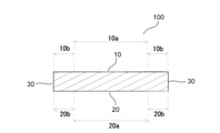
- FIG. 1 is a typical schematic cross-sectional view of a group III element nitride semiconductor substrate according to an embodiment of the present invention.
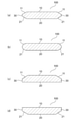
- 2 (a) to 2 (d) are schematic cross-sectional views of the group III element nitride semiconductor substrate according to the embodiment of the present invention, the ends of which are different from those of the embodiment shown in FIG. It is a schematic plan view seen from the main surface direction of the group III element nitride semiconductor substrate by embodiment of this invention. It is a schematic plan view seen from the back surface direction of the group III element nitride semiconductor substrate by embodiment of this invention. It is a schematic explanatory drawing which shows the manufacturing method of the group III element nitride semiconductor substrate by embodiment of this invention.
- weight When the expression “weight” is used in this specification, it may be read as “mass” which is commonly used as an SI system unit indicating weight.
- the group III element nitride semiconductor substrate according to the embodiment of the present invention is typically a self-standing substrate made of group III element nitride crystals.
- the "self-supporting substrate” means a substrate that can be handled as a solid substance without being deformed or damaged by its own weight when handled.
- the self-supporting substrate can be used as a substrate for various semiconductor devices such as light emitting elements and power control elements.
- the group III element nitride semiconductor substrate according to the embodiment of the present invention is typically in the shape of a wafer (substantially a perfect circle).
- the size thereof is preferably 20 mm to 310 mm in diameter, and typically 25 mm (about 1 inch) and 45 to 55 mm. (About 2 inches), 95 to 105 mm (about 4 inches), 145 to 155 mm (about 6 inches), 195 to 205 mm (about 8 inches), 295 to 305 mm (about 12 inches), and the like.
- the group III element nitride semiconductor substrate according to the embodiment of the present invention can be easily applied to the manufacturing process of a semiconductor package. If necessary, it may be processed into a shape other than that, for example, a shape such as a rectangle.
- the thickness of the group III element nitride semiconductor substrate according to the embodiment of the present invention is preferably 300 ⁇ m to 1000 ⁇ m.
- group III element nitride examples include gallium nitride (GaN), aluminum nitride (AlN), indium nitride (InN), or a mixed crystal thereof. These may be only one kind or two or more kinds.
- group III element nitride examples include GaN, AlN, InN, Ga x Al 1-x N (1>x> 0), Ga x In 1-x N (1>x> 0), and Al x .
- In 1-x N (1>x> 0), Ga x Aly In z N (1>x> 0, 1>y> 0, x + y + z 1).
- These may be doped with various n-type dopants or p-type dopants.
- p-type dopant examples include beryllium (Be), magnesium (Mg), strontium (Sr), and cadmium (Cd). These may be only one kind or two or more kinds.
- n-type dopant examples include silicon (Si), germanium (Ge), tin (Sn), and oxygen (O). These may be only one kind or two or more kinds.
- the plane orientation of the group III element nitride semiconductor substrate can be a specific crystal plane inclined from the c-plane, m-plane, a-plane, and c-plane, a-plane, and m-plane, and in particular, the c-plane. At this time, the effect of the present invention is more exhibited.
- a so-called semi-polar plane such as a ⁇ 11-22 ⁇ plane or a ⁇ 20-21 ⁇ plane can be exemplified.
- the plane orientation may include not only a so-called just plane perpendicular to the c-plane, a-plane, m-plane or a specific crystal plane inclined from these, but also an off angle in the range of ⁇ 5 °. Permissible.
- the group III element nitride semiconductor substrate according to the embodiment of the present invention is a group III element nitride semiconductor substrate including a first surface and a second surface, wherein the first surface is a mirror surface and the second surface is a mirror surface. It has a second surface central region and a second surface outer peripheral region, the second surface central region is a mirror surface, and the second surface outer peripheral region is a non-mirror surface.
- the main surface when the first surface is the main surface and the second surface is the back surface, if the surface orientation of the group III element nitride semiconductor substrate is the c surface, the main surface. Is typically a group III element polar plane, and the back surface is typically a nitrogen polar plane. However, depending on the application, various devices may be manufactured on the polar surface of nitrogen, and the main surface may be the polar surface of nitrogen, or the back surface may be the polar surface of Group III elements. Various devices can be mounted on the main surface, and epitaxial crystals can be grown. The back surface can be held by a susceptor or the like to transfer the group III element nitride semiconductor substrate according to the embodiment of the present invention.
- the first surface will be described as the main surface and the second surface as the back surface. Therefore, in the present specification, what is referred to as “main surface” may be read as “first surface”, and what is referred to as “first surface” may be read as “main surface” and is referred to as “back surface”. Things may be read as “second side”, and “second side” may be read as “back side”.
- FIG. 1 is a typical schematic cross-sectional view of a group III element nitride semiconductor substrate according to the embodiment of the present invention.
- the group III element nitride semiconductor substrate 100 typically includes a main surface 10, a back surface 20, and a side surface 30 which are in a front-to-back relationship, and the main surface 10 has a main surface 10.
- the back surface 20 has a main surface central region 10a and a main surface outer peripheral region 10b, and the back surface 20 has a back surface central region 20a and a back surface outer peripheral region 20b.
- the main surface 10 has a main surface central region 10a and a main surface outer peripheral region 10b, but unlike this, the main surface has a main surface central region and a main surface outer peripheral region. You don't have to.
- the end portion of the group III element nitride semiconductor substrate according to the embodiment of the present invention may take any appropriate form as long as the effect of the present invention is not impaired. That is, the cross-sectional shape of the end portion of the group III element nitride semiconductor substrate according to the embodiment of the present invention is not only a rectangular shape as shown in FIG. 1, but for example, both the main surface side and the back surface side are flat surfaces. It may have a chamfered shape (FIG. 2 (a)) or an R-shaped chamfered shape (FIG. 2 (b)), and only the main surface side of the end is a flat surface. It may be a shape chamfered so as to be (FIG.
- the main surface side and the back surface side of the end portion are chamfered, and the main surface chamfering portion 11 and the back surface side chamfering portion 21 are provided.
- the main chamfered portion 11 and the back surface chamfered portion 21 are curved surfaces chamfered in an R shape. The curved surfaces meet at the outer edges, leaving no flat sides.
- the main surface side surface removing portion 11 is provided, the back surface does not have the back surface side surface removing portion, and the main surface side surface removing portion is provided.
- Reference numeral 11 is a flat surface, and the flat surface is inclined with respect to the main surface 10, the back surface 20, and the side surface 30, and the side surface 30 is a flat surface.
- the back surface side surface portion 21 is provided, the main surface does not have the main surface side surface removal portion, and the back surface side surface removal portion is provided.
- the end portion of the group III element nitride semiconductor substrate according to the embodiment of the present invention is not limited to the embodiment shown in FIGS. 2 (a) to 2 (d).
- the main surface side surface portion 11 may be provided over the entire main surface outer peripheral region 10b (entire one circumference), or may be provided only on a part of the main surface outer peripheral region 10b. From the viewpoint of suppressing chipping of the semiconductor substrate, the main surface side surface portion 11 is preferably provided over the entire main surface outer peripheral region 10b (the entire circumference).
- the back surface side surface removing portion 21 may be provided over the entire back surface outer peripheral region 20b (entire one round), or may be provided only in a part of the back surface outer peripheral region 20b. From the viewpoint of suppressing chipping of the semiconductor substrate and the like, preferably, the back surface side surface portion 21 is provided over the entire back surface outer peripheral region 20b (the entire circumference).
- the main surface is a mirror surface. That is, when the main surface 10 has a main surface central region 10a and a main surface outer peripheral region 10b as shown in FIG. 1, both the main surface central region 10a and the main surface outer peripheral region 10b are mirror surfaces.
- the back surface has a back surface center region and a back surface outer peripheral region, the back surface center region is a mirror surface, and the back surface outer peripheral region is a non-mirror surface. That is, in FIG. 1, the back surface central region 20a is a mirror surface, and the back surface outer peripheral region 20b is a non-mirror surface.
- the group III element nitride semiconductor substrate according to the embodiment of the present invention has a chamfered shape so that the back surface side becomes a flat surface, for example, as shown in FIGS. 2A, 2B, and 2D.
- the back surface chamfering portion may coincide with the back surface outer peripheral region of the back surface. That is, in FIGS. 2A, 2B, and 2D, the back surface side surface portion 21 may coincide with the back surface outer peripheral region 20b. Also in this case, since the back surface outer peripheral region 20b is a non-mirror surface, the back surface side surface portion 21 is also a non-mirror surface.
- the main surface is a mirror surface
- the center region of the back surface is a mirror surface
- the outer peripheral region of the back surface is a non-mirror surface. That is, in the group III element nitride semiconductor substrate according to the embodiment of the present invention, among the main surface and the back surface, only the back surface outer peripheral region is a non-mirror surface, and the others are mirror surfaces.
- the group III element nitride semiconductor substrate according to the embodiment of the present invention is a group III element nitride semiconductor substrate of the front and back double-sided mirror surface type in which only the outer peripheral region of the back surface is non-mirror-finished.
- a mirror surface is a mirror-finished surface, and after mirror-finishing, the roughness and waviness of the surface are reduced until it is possible to visually confirm that light is reflected and an object is reflected on the mirror-finished surface.
- the surface in the state of being That is, the surface is in a state where the roughness and the size of the waviness of the surface after mirror processing are sufficiently reduced to a negligible level with respect to the wavelength of visible light. Epitaxial crystal growth is sufficiently possible on the mirrored surface.
- any appropriate method can be adopted as long as the effect of the present invention is not impaired.
- a method include a polishing device using a tape, a lapping device using diamond abrasive grains, a CMP (Chemical Mechanical Polish) device using a slurry such as colloidal silica and a non-woven fabric polishing pad, and the like.
- Examples thereof include a method of mirroring using one or a combination.
- the non-mirror surface is a surface that has not been mirror-processed, and typically, a rough surface obtained by roughening treatment can be mentioned.
- any appropriate method can be adopted as long as the effect of the present invention is not impaired.
- Examples of such a method include laser texture processing, etching treatment using various chemicals and gases, physical or chemical coating treatment, and machining by machining.
- the surface roughness Ra of the back surface outer peripheral region is preferably 100 nm or more, more preferably 200 nm to 1500 nm, and further preferably 500 nm to 1000 nm.
- the surface roughness Ra of the central region of the back surface is preferably 10 nm or less, more preferably 0.1 nm to 2 nm, further preferably 0.1 nm to 1 nm, and particularly preferably 0.1 nm to 0.5 nm. be.
- the surface roughness Ra of the main surface is preferably 2 nm or less, more preferably 1 nm or less, further preferably 0.1 nm to 0.5 nm, and particularly preferably 0.1 nm to 0.2 nm.
- the warp of the substrate is small, preferably 50 ⁇ m or less, more preferably 40 ⁇ m. It is less than or equal to, and more preferably 30 ⁇ m or less. If the warp of the substrate is larger than 50 ⁇ m, manufacturing defects may occur due to variations in the film thickness of the film forming apparatus and defocusing of the exposure apparatus for semiconductor circuits when various devices are manufactured using the semiconductor substrate.
- the warp of the substrate is small and the radius of curvature is preferably 30 m or more. It is more preferably 50 m or more, further preferably 70 m or more, and particularly preferably 100 m or more. If the radius of curvature is smaller than 30 m, when various devices are manufactured using a semiconductor substrate, the substrate cannot be fixed by adsorption inside the process device or on the transport device, and manufacturing defects may occur due to the substrate falling off. ..
- the group III element nitride semiconductor substrate according to the embodiment of the present invention can be easily visually distinguished from the main surface and the back surface, it is not necessary to form a sub-orientation flat (sub-orifura), and the effective area of the semiconductor substrate (device fabrication). A large area that can be used for That is, the group III element nitride semiconductor substrate according to the embodiment of the present invention preferably does not have a sub-orientation flat.
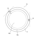
- FIG. 3 is a schematic plan view of the group III element nitride semiconductor substrate according to the embodiment of the present invention as viewed from the main surface direction.
- the main surface side surface taking portion 11 may be provided on the main surface.
- the main surface side surface portion 11 is typically a region provided in the main surface outer peripheral region 10b from the outer peripheral end portion 12 to the distance of the width D1 from the outer peripheral end portion 12 toward the inside of the main surface 10.
- the width D1 of the side surface portion of the main surface is a distance starting from the outer peripheral end portion 12 and is a distance in the normal direction with respect to the tangential line at the outer peripheral end portion 12 toward the inside of the main surface 10. It is preferable that the width D1 of the main surface side surface removing portion is constant in the entire main surface side surface removing portion 11.
- FIG. 4 is a schematic plan view of the group III element nitride semiconductor substrate according to the embodiment of the present invention as viewed from the back surface direction.
- the back surface side surface removing portion 21 may be provided on the back surface.
- the back surface side surface portion 21 is typically a region provided in the back surface outer peripheral region 20b from the outer peripheral end portion 22 to the distance of the width D2 from the outer peripheral end portion 22 toward the inside of the back surface 20 over the entire circumference.
- the width D2 of the back surface side surface portion is a distance starting from the outer peripheral end portion 22 and is a distance in the normal direction with respect to the tangential line at the outer peripheral end portion 22 toward the inner side of the back surface 20. It is preferable that the width D2 of the back surface side surface removing portion is constant in the entire back surface side surface removing portion 21.
- the back surface outer peripheral region 20b is typically a region from the outer peripheral end portion 22 when the back surface 20 is viewed from a plane direction to a distance of a width d2 from the outer peripheral end portion 22 toward the inside of the back surface 20. ..
- the width d2 of the outer peripheral region of the back surface is a distance starting from the outer peripheral end portion 22 and is a distance in the normal direction with respect to the tangent line at the outer peripheral end portion 22 toward the inside of the back surface 20. Is.
- the width d2 of the back surface outer peripheral region is preferably constant over the entire back surface outer peripheral region 20b.
- the width d2 of the outer peripheral region of the back surface may be any appropriate size as long as the effect of the present invention is not impaired, depending on the size of the group III element nitride semiconductor substrate according to the embodiment of the present invention.
- the width d2 of the outer peripheral region of the back surface is preferably 5 mm or less, more preferably 3 mm or less, and further preferably 1 mm or less in that the effect of the present invention can be more exhibited.
- the lower limit of the width d2 of the back surface outer peripheral region is preferably 0.2 mm or more, and more preferably 0.5 mm or more in that the effect of the present invention can be more exhibited.
- the back surface side surface portion may coincide with the back surface outer peripheral region of the back surface.
- the back surface side surface portion 21 may coincide with the back surface outer peripheral region 20b.
- the width D2 of the back surface side surface portion coincides with the width d2 of the back surface outer peripheral region.
- the back surface outer peripheral region 20b is preferably a light shielding region that attenuates the laser beam of 450 nm to 1100 nm. Since the back surface outer peripheral region 20b is a light-shielding region that attenuates the laser beam of 450 nm to 1100 nm, it is possible to easily visually distinguish between the main surface and the back surface, and it is possible to easily detect the end portion by the optical sensor. In the group III element nitride semiconductor substrate according to the embodiment of the present invention, the back surface outer peripheral region 20b is more preferably a light shielding region that attenuates laser light having a wavelength of 650 nm by 10% or more.
- the warp of the group III element nitride semiconductor substrate according to the embodiment of the present invention is preferably 50 ⁇ m or less. The measurement of warpage will be described later.
- the Group III element nitride semiconductor substrate according to the embodiment of the present invention has a radius of curvature of preferably 30 m or more, more preferably 40 m or more, and further preferably 50 m or more. The measurement of the radius of curvature will be described later.
- the group III element nitride semiconductor substrate according to the embodiment of the present invention can be produced by any suitable method as long as the effect of the present invention is not impaired.
- the group III element nitride semiconductor substrate according to the embodiment of the present invention typically has a seed crystal film 2 formed on the main surface 1a of the base substrate 1 as shown in FIG. 5 (a).
- the group III element nitride layer 3 is formed on the group III element polar surface 2a of 2.
- the group III element nitride layer (seed crystal film 2 + group III element nitride layer 3) to be a self-supporting substrate is separated from the base substrate 1 to obtain a self-supporting substrate 100'having a main surface 10'and a back surface 20'.
- the base substrate 1 is irradiated with laser light from the back surface 1b side as shown by arrow A and the group III element nitride layer is separated by the laser lift-off method to obtain a self-supporting substrate 100'as shown in FIG. 5 (b).
- any suitable material can be adopted as long as the effect of the present invention is not impaired.
- examples of such a material include sapphire, crystal oriented alumina, gallium oxide, Al x Ga 1-x N (0 ⁇ x ⁇ 1), GaAs, and SiC.
- any suitable material can be adopted as long as the effect of the present invention is not impaired.
- examples of such a material include Al x Ga 1-x N (0 ⁇ x ⁇ 1) and In x Ga 1-x N (0 ⁇ x ⁇ 1), and gallium nitride is preferable.
- the material of the seed crystal film is more preferably gallium nitride, which has a yellow light emitting effect when observed with a fluorescence microscope. Yellow emission is a peak (yellow emission (YL) or yellow band (YB)) that appears in the range of 2.2 to 2.5 eV in addition to the band-to-band exciton transition (UV).
- any appropriate forming method can be adopted as long as the effect of the present invention is not impaired.
- a forming method include a gas phase growth method, preferably a metalorganic chemical vapor deposition (MOCVD) method, a hydride vapor phase growth (HVPE) method, and pulse-pumped deposition.
- MOCVD metalorganic chemical vapor deposition
- HVPE hydride vapor phase growth
- PXD the metalorganic chemical vapor deposition
- MBE method the sublimation method.
- the metalorganic chemical vapor deposition method MOCVD: Metalorganic Chemical Vapor Deposition
- the growth temperature is preferably 950 to 1200 ° C.
- any appropriate growth direction can be adopted as long as the effect of the present invention is not impaired.
- a growth direction for example, the normal direction of the c-plane of the wurtzite structure, the normal direction of each of the a-plane and the m-plane, and the normal direction of the plane inclined from each of the c-plane, the a-plane and the m-plane are used. Can be mentioned.
- any appropriate method can be adopted as long as the effect of the present invention is not impaired.
- a production method include a metalorganic chemical vapor deposition (MOCVD) method, a hydride vapor phase deposition (HVPE) method, a pulse excited deposition (PXD) method, an MBE method, and a sublimation method.
- MOCVD metalorganic chemical vapor deposition
- HVPE hydride vapor phase deposition
- PXD pulse excited deposition
- MBE method an MBE method
- sublimation method a sublimation method.
- a vapor phase method; a liquid phase method such as an amonothermal method and a flux method; can be mentioned.
- the outer peripheral portion of the self-standing substrate is ground to form a circular shape with a desired diameter.
- any appropriate size can be adopted as long as the effect of the present invention is not impaired.
- Such sizes include, for example, 25 mm (about 1 inch), 45 to 55 mm (about 2 inches), 95 to 105 mm (about 4 inches), 145 to 155 mm (about 6 inches), and 195 to 205 mm (about 8 inches). ), 295 to 305 mm (about 12 inches), etc.
- the plate is thinned to a desired thickness and the surface of the group III element polar surface is flattened, and the group III element polar surface is mirrored. Obtain a free-standing substrate.
- the group III element polar surface of the self-supporting substrate whose group III element polar surface is mirrored is attached to the processing platen.
- the wax thickness is changed by adjusting the load applied to the self-supporting substrate, or a jig is sandwiched between the self-supporting substrate and the processing platen to change the surface shape of the self-standing substrate.
- the plate is thinned to a desired thickness and the surface of the nitrogen polar surface is flattened to obtain a self-standing substrate with the nitrogen polar surface mirrored.
- the polar surface of the group III element is mirror-finished and then the polar surface of the nitrogen is mirror-finished, but the order may be reversed.
- the thickness of the self-standing substrate after polishing (the thickness of the maximum thickness portion when the thickness is not constant) is preferably 300 ⁇ m to 1000 ⁇ m.
- the outer peripheral edge of the self-supporting substrate is chamfered by grinding, and finally, the group III element nitride semiconductor substrate 100 according to the embodiment of the present invention is obtained.
- chamfering can be performed by any appropriate chamfering method as long as the effect of the present invention is not impaired.
- Examples of such a chamfering method include grinding using a diamond grindstone, polishing using a tape, and CMP (Chemical Mechanical Polish) using a slurry such as colloidal silica and a polishing pad of a non-woven fabric. ..
- the outer peripheral portion of the nitrogen polar surface is roughened, and finally, the Group III element nitride semiconductor substrate 100 according to the embodiment of the present invention is obtained.
- any appropriate method can be adopted as long as the effect of the present invention is not impaired.
- Examples of such a method include laser texture processing, etching treatment using various chemicals and gases, physical or chemical coating treatment, and machining by machining.
- crystals can be epitaxially grown on the main surface (group III element polar surface) 10, and the functional layer 4 is formed as shown in FIG. 5 (c).
- Reference numeral 20 is a back surface (nitrogen polar surface).
- the thickness distribution (TTV: Total Tickness Variation) of the self-supporting substrate occurs.
- TTV Total Tickness Variation
- the thickness distribution of the free-standing substrate occurs, a large distribution does not occur on the main surface (group III element polar plane) when the functional layer is epitaxially grown on the free-standing substrate. This is because it utilizes the property that the group III element nitride crystals constituting the self-supporting substrate have high thermal conductivity. As a result, morphology abnormality does not occur at the time of film formation of the functional layer, and the emission wavelength deviation and the variation of the voltage-current characteristics can be sufficiently suppressed.
- Examples of the epitaxial crystal to be grown on the obtained group III element nitride semiconductor substrate include gallium nitride, aluminum nitride, indium nitride, or a mixed crystal thereof.
- Specific examples of such an epitaxial crystal include GaN, AlN, InN, Ga x Al 1-x N (1>x> 0), and Ga x In 1-x N (1>x> 0).
- examples of the functional layer provided on the obtained Group III element nitride semiconductor substrate include a rectifying element layer, a switching element, and a power semiconductor layer. Further, by providing a functional layer on the group III element polar surface of the obtained group III element nitride semiconductor substrate and then processing, for example, grinding and polishing the nitrogen polar surface, the thickness and thickness distribution of the self-supporting substrate are distributed. Can also be made smaller.
- the surface of the group III element nitride semiconductor self-standing substrate was 1.4 mm x 1 using a non-contact surface shape measuring machine (Zygo, New View 7000, objective lens x 5 times, software: MetroPro 9.0.10).
- the surface roughness (arithmetic mean roughness) Ra was calculated with an observation field of 0.05 mm.
- Ra of the main surface and the back surface central region is measured at the center of the substrate, and Ra of the back surface outer peripheral region corresponds to d2 / 2 from the boundary between the back surface center region and the back surface outer peripheral region when the width of the back surface outer peripheral region is d2. Measured at position.
- the width d2 of the back surface outer peripheral region was narrower than the observation field of view of 1.4 mm ⁇ 1.05 mm, the observation field of view was appropriately narrowed and the measurement was carried out.
- ⁇ Evaluation criteria for edge detection by optical sensor> A transmission test was performed using a transmissive photoelectric sensor to detect the edge of the substrate.
- a ZX-GT28S (wavelength 650 nm) manufactured by OMRON Corporation was used as a light source and a detector, the binarization level of the measured value was set to 50%, and the attenuation rate at the wavelength of 650 nm was evaluated.
- the laser intensity that allows the edge intensity of the transmissive photoelectric sensor was confirmed using a laser power sensor (3A manufactured by Ophir).
- ⁇ The laser beam having a wavelength of 650 nm can be attenuated by 10% or more (sensor judgment: possible).
- X The laser beam having a wavelength of 650 nm cannot be attenuated by 10% or more (sensor determination: impossible).
- Warpage can be measured by a laser displacement meter.
- a laser displacement meter is a device that measures the displacement of each surface by irradiating each surface with a laser beam.
- the wavelength of the laser is 655 nm, and a confocal method, a triangular distance measuring method, and an optical interference method can be used as the measuring method depending on the surface roughness.
- a waveform was obtained except for a range of 3 mm in width from the edge of the substrate.
- an approximate curve for this waveform is obtained by the least squares method using a quadratic function, and the difference between the maximum value and the minimum value of this approximate curve is measured on two orthogonal axes on the substrate surface, and the two values are measured.
- the average value was set to warp S.
- Example 1 A gallium nitride film having a thickness of 2 ⁇ m was formed on a 6-inch c-plane sapphire wafer by the MOCVD method to prepare a seed crystal substrate.
- This seed crystal substrate was placed in an alumina crucible having a diameter of 200 mm in a glove box having a nitrogen atmosphere.
- the crucible was placed in a stainless steel inner container, then in a stainless steel outer container that could hold it, and closed with a container lid with a nitrogen inlet pipe.
- This outer container was placed on a rotary table installed in a heating section in a crystal manufacturing apparatus that had been vacuum-baked in advance, and the pressure-resistant container was covered and sealed.
- the inside of the pressure-resistant container was evacuated to 0.1 Pa or less with a vacuum pump.
- nitrogen gas is introduced from the nitrogen gas cylinder up to 4.0 MPa, and the outer container is rotated around the central axis. It was rotated clockwise and counterclockwise at a constant cycle at a speed of 20 rpm. Then, it was held in this state for 40 hours.
- the lid of the pressure-resistant container was opened and the crucible was taken out from the inside.
- the solidified metallic sodium in the crucible was removed, and the gallium nitride crystal grown on the seed crystal substrate was recovered.
- the gallium nitride crystal on the seed crystal substrate was decomposed by irradiating the sapphire wafer side with an ultraviolet laser, and the grown gallium nitride crystal was separated from the sapphire wafer.
- the warp of the gallium nitride crystal obtained by separation was 50 ⁇ m.
- the outer peripheral portion of the gallium nitride crystal was ground using a diamond grindstone to adjust the diameter to 150 mm.
- the gallium nitride crystal was attached to a ceramic processing surface plate, and the Ga polar surface was ground and polished using a grinder and a lapping device.
- diamond abrasive grains with a particle size of 0.1 ⁇ m were used to achieve a mirror finish.
- the gallium nitride crystal was turned inside out and fixed to a ceramic processing surface plate, and the nitrogen polar surface was similarly ground and polished.
- diamond abrasive grains with a particle size of 0.1 ⁇ m were used to achieve a mirror finish.
- a protective material was applied to the front and back surfaces of the gallium nitride crystal, and the outer peripheral portion of the wafer was molded using a beveling device.
- the Ga polar surface was chamfered using an inclined grindstone (inclination angle of 20 degrees).
- the chamfer width D1 was set to 150 ⁇ m.
- the nitrogen polar surface was roughened on the outer circumference by laser texture processing.
- An ultraviolet laser having a wavelength of 355 nm and an output of 3 W was used, and a concavo-convex shape was formed on the outer peripheral portion by irradiating while scanning a laser focused on a diameter of 70 ⁇ m.
- the range d2 of the roughening process was set to 3 mm from the outer circumference.
- the front and back surfaces of the obtained Group III element nitride semiconductor wafer could be easily identified visually.
- the warpage of the wafer was 40 ⁇ m. The results are shown in Table 1.
- Example 2 A group III element nitride semiconductor wafer was produced in the same manner as in Example 1 except that the range d2 of the back surface roughening process was set to 5 mm from the outer circumference. The front and back surfaces of the obtained Group III element nitride semiconductor wafer could be easily visually identified. The warpage of the wafer was 48 ⁇ m. The results are shown in Table 1.
- Example 3 A group III element nitride semiconductor wafer was produced in the same manner as in Example 1 except that the range d2 of the back surface roughening process was set to 1 mm from the outer circumference. The front and back surfaces of the obtained Group III element nitride semiconductor wafer could be visually identified. The warpage of the wafer was 28 ⁇ m. The results are shown in Table 1.
- Example 1 A group III element nitride semiconductor wafer was produced in the same manner as in Example 1 except that the entire back surface was rough-finished. The front and back surfaces of the obtained Group III element nitride semiconductor wafer could be easily visually identified. The warpage of the wafer was 105 ⁇ m. The results are shown in Table 1.
- Example 2 A group III element nitride semiconductor wafer was produced in the same manner as in Example 1 except that the range d2 of the back surface roughening process was set to 10 mm from the outer circumference. The front and back surfaces of the obtained Group III element nitride semiconductor wafer could be easily identified visually. The warpage of the wafer was 59 ⁇ m. The results are shown in Table 1.
- Example 3 A group III element nitride semiconductor wafer was produced in the same manner as in Example 1 except that the entire back surface was mirror-finished. The front and back surfaces of the obtained Group III element nitride semiconductor wafer could not be visually identified. The warpage of the wafer was 21 ⁇ m. The results are shown in Table 1.
- the group III element nitride semiconductor substrate according to the embodiment of the present invention can be used as a substrate for various semiconductor devices.
- Group III element nitride semiconductor substrate 100'Self-supporting substrate 1 Base substrate 1a Main surface of base substrate 1b Back surface of base substrate 1 Type 2 crystal film 2a Group III element polar surface of type crystal film 2 Group III element nitride layer 4 Functional layer 5 Functional element 10 Main surface 10'Main surface 10a Main surface central area 10b Main surface outer peripheral area 11 Main surface side surface trimming part 12 Outer peripheral end 20 Back surface 20' Back surface 20a Back surface center area 20b Back surface outer peripheral area 21 Back surface side surface Part 22 Outer peripheral end 30 Side surface
Landscapes
- Chemical & Material Sciences (AREA)
- Engineering & Computer Science (AREA)
- Crystallography & Structural Chemistry (AREA)
- Materials Engineering (AREA)
- Metallurgy (AREA)
- Organic Chemistry (AREA)
- Inorganic Chemistry (AREA)
- Mechanical Engineering (AREA)
- Ceramic Engineering (AREA)
- Crystals, And After-Treatments Of Crystals (AREA)
- Led Devices (AREA)
Abstract
第一面と第二面とを備えるIII族元素窒化物半導体基板であって、目視による第一面と第二面の区別が容易であり、光学センサーによる端部の検出がしやすく、有効面積(デバイス作製に使用できる面積)を大きく確保でき、基板全体の反りが低減される、III族元素窒化物半導体基板を提供する。 本発明の実施形態によるIII族元素窒化物半導体基板は、第一面と第二面とを備えるIII族元素窒化物半導体基板であって、該第一面が鏡面であり、該第二面が第二面中央領域と第二面外周領域とを有し、該第二面中央領域が鏡面であり、該第二面外周領域が非鏡面である。
Description
本発明はIII族元素窒化物半導体基板に関する。より詳細には、第一面と第二面とを備えるIII族元素窒化物半導体基板であって、第二面の外周領域のみを非鏡面仕上げとした、表裏両面鏡面タイプのIII族元素窒化物半導体基板に関する。
各種半導体デバイスの基板として、窒化ガリウム(GaN)ウエハ、窒化アルミニウム(AlN)ウエハ、窒化インジウム(InN)ウエハなどのIII族元素窒化物半導体基板が用いられている(例えば、特許文献1など)。
半導体基板は、第一面と第二面とを備える。第一面を主面、第二面を裏面としたとき、主面は、一般的に、鏡面仕上げされる。他方、裏面は、用途に応じて、鏡面仕上げされるか粗面仕上げされる(例えば、特許文献2-4など)。
裏面が鏡面仕上げされた場合は、主面と裏面との両方が鏡面となるため、目視による主面と裏面の区別が困難になる。このため、通常のオリエンテーションフラット(オリフラ)に加えて、サブオリエンテーションフラット(サブオリフラ)を形成することによって、目視による主面と裏面の区別を行っている。
しかし、通常のオリエンテーションフラット(オリフラ)に加えて、サブオリエンテーションフラット(サブオリフラ)を形成すると、半導体基板の有効面積(デバイス作製に使用できる面積)が小さくなってしまうという問題が生じる。
また、半導体基板の自動化製造プロセスにおいては、半導体基板の端部を光学センサーによって検出する。この場合、半導体基板が透明であって、且つ、裏面が鏡面仕上げされていると、測定光が半導体基板を実質的に透過してしまうために、光源から出力される光量と検出器に入力される光量との変化量が非常に小さくなり、光学センサーが検知しない場合が生じるため、該半導体基板の端部の検出エラーが発生しやすくなり、自動化製造プロセスが停止してしまうという問題が生じる。
他方、裏面が粗面仕上げされた場合は、目視による主面と裏面の区別はしやすく、また、上記のような光学センサーによる端部の検出エラーも起こりにくい。しかしながら、基板全体に反りが発生しやすいという問題が生じる。これは、主面と裏面の物理的な表面状態が異なるためと考えられる(例えば、特許文献3、4など)。半導体基板を用いて各種デバイスを作製する際に、製造プロセス装置の動作不良を抑制する観点から、反りは小さいほどよい。ここで、動作不良とは、成膜装置の膜厚バラツキや半導体回路用露光装置の焦点ズレ、移載装置の吸着不良などが例示される。
本発明の課題は、第一面と第二面とを備えるIII族元素窒化物半導体基板であって、目視による第一面と第二面の区別が容易であり、光学センサーによる端部の検出がしやすく、有効面積(デバイス作製に使用できる面積)を大きく確保でき、基板全体の反りが低減される、III族元素窒化物半導体基板を提供することにある。
本発明の課題を解決するためには、第一面と第二面とを備えるIII族元素窒化物半導体基板において、従来にはない新たな基板設計が求められる。第一面を主面、第二面を裏面としたとき、反りを低減するためには、例えば、主面と裏面の物理的な表面状態をできるだけ同じとする設計、具体的には、主面と裏面をいずれも鏡面とする設計が考えられる。しかし、裏面を鏡面とすると、光学センサーによる端部の検出エラーが発生しやすくなる。また、主面と裏面の物理的な表面状態をできるだけ同じとする設計を行った場合、目視による主面と裏面の区別を容易に行うためには主面と裏面で何らかの見分け箇所を設ける必要がある。従来、この見分け箇所として、サブオリエンテーションフラット(サブオリフラ)が形成されているが、有効面積(デバイス作製に使用できる面積)が小さくなってしまうため、別の見分け手段を構築する必要がある。
上記のような新たな基板設計について検討を行った結果、第一面と第二面とを備えるIII族元素窒化物半導体基板において、第一面を主面、第二面を裏面としたとき、裏面の外周領域に着目し、裏面の外周領域のみを非鏡面仕上げとした表裏両面鏡面タイプの基板とすれば、上記課題が解決できることに想到し、本発明を完成するに至った。
本発明の実施形態によるIII族元素窒化物半導体基板は、
第一面と第二面とを備えるIII族元素窒化物半導体基板であって、
該第一面が鏡面であり、
該第二面が第二面中央領域と第二面外周領域とを有し、
該第二面中央領域が鏡面であり、
該第二面外周領域が非鏡面である。
第一面と第二面とを備えるIII族元素窒化物半導体基板であって、
該第一面が鏡面であり、
該第二面が第二面中央領域と第二面外周領域とを有し、
該第二面中央領域が鏡面であり、
該第二面外周領域が非鏡面である。
一つの実施形態においては、上記第二面外周領域の幅が5mm以下である。
一つの実施形態においては、上記第二面外周領域の幅が3mm以下である。
一つの実施形態においては、上記第二面外周領域の幅が1mm以下である。
一つの実施形態においては、上記第二面外周領域の表面粗さRaが100nm以上である。
一つの実施形態においては、上記第二面中央領域の表面粗さRaが10nm以下である。
一つの実施形態においては、上記第一面の表面粗さRaが1nm以下である。
一つの実施形態においては、上記第二面外周領域は、波長650nmのレーザ光を10%以上減衰させる遮光領域である。
一つの実施形態においては、上記基板の反りが50μm以下である。
一つの実施形態においては、上記基板の曲率半径が30m以上である。
一つの実施形態においては、本発明の実施形態によるIII族元素窒化物半導体基板は、サブオリエンテーションフラットを有しない。
一つの実施形態においては、本発明の実施形態によるIII族元素窒化物半導体基板は、直径が95mm以上である。
一つの実施形態においては、本発明の実施形態によるIII族元素窒化物半導体基板は、直径が145mm以上である。
本発明によれば、第一面と第二面とを備えるIII族元素窒化物半導体基板であって、目視による第一面と第二面の区別が容易であり、光学センサーによる端部の検出がしやすく、有効面積を大きく確保でき、基板全体の反りが低減される、III族元素窒化物半導体基板を提供することができる。
本明細書中で「重量」との表現がある場合は、重さを示すSI系単位として慣用されている「質量」と読み替えてもよい。
本発明の実施形態によるIII族元素窒化物半導体基板は、代表的には、III族元素窒化物結晶からなる自立基板である。本発明の説明において、「自立基板」とは、取り扱う際に自重で変形または破損せず、固形物として取り扱うことのできる基板を意味する。自立基板は発光素子や電力制御素子等の各種半導体デバイスの基板として使用可能である。
本発明の実施形態によるIII族元素窒化物半導体基板は、代表的には、ウエハ状(略真円状)である。本発明の実施形態によるIII族元素窒化物半導体基板がウエハ状の場合、その大きさは、直径が、好ましくは20mm~310mmであり、代表的には、25mm(約1インチ)、45~55mm(約2インチ)、95~105mm(約4インチ)、145~155mm(約6インチ)、195~205mm(約8インチ)、295~305mm(約12インチ)等である。このような大きさであれば、本発明の実施形態によるIII族元素窒化物半導体基板は、半導体パッケージの製造工程に適用し易くなる。なお、必要に応じて、それ以外の形状、例えば、矩形等の形状に加工してもよい。
本発明の実施形態によるIII族元素窒化物半導体基板は、その厚さ(厚さが一定でない場合は最大厚さ箇所の厚さ)が、好ましくは300μm~1000μmである。
III族元素窒化物としては、代表的には、窒化ガリウム(GaN)、窒化アルミニウム(AlN)、窒化インジウム(InN)またはこれらの混晶が挙げられる。これらは、1種のみであってもよいし、2種以上であってもよい。
III族元素窒化物は、具体的には、GaN、AlN、InN、GaxAl1-xN(1>x>0)、GaxIn1-xN(1>x>0)、AlxIn1-xN(1>x>0)、GaxAlyInzN(1>x>0、1>y>0、x+y+z=1)である。これらは、各種のn型ドーパントまたはp型ドーパントでドープされていてもよい。
p型ドーパントとしては、代表的には、ベリリウム(Be)、マグネシウム(Mg)、ストロンチウム(Sr)、およびカドミウム(Cd)が挙げられる。これらは、1種のみであってもよいし、2種以上であってもよい。
n型ドーパントとしては、代表的には、シリコン(Si)、ゲルマニウム(Ge)、スズ(Sn)、および酸素(O)が挙げられる。これらは、1種のみであってもよいし、2種以上であってもよい。
III族元素窒化物半導体基板の面方位は、c面、m面、a面、およびc面、a面、m面それぞれから傾斜した特定の結晶面とすることができ、特に、c面とした際に本発明の効果がより発現される。c面、a面、m面それぞれから傾斜した特定の結晶面としては、{11-22}面や{20-21}面といった、いわゆる半極性面が例示できる。また、面方位としては、c面、a面、m面あるいはこれらから傾斜した特定の結晶面に対して、垂直ないわゆるジャスト面だけでなく、±5°の範囲でのオフ角を含むことが許容される。
本発明の実施形態によるIII族元素窒化物半導体基板は、第一面と第二面とを備えるIII族元素窒化物半導体基板であって、該第一面が鏡面であり、該第二面が第二面中央領域と第二面外周領域とを有し、該第二面中央領域が鏡面であり、該第二面外周領域が非鏡面である。
本発明の実施形態によるIII族元素窒化物半導体基板において、第一面を主面、第二面を裏面としたとき、III族元素窒化物半導体基板の面方位がc面であれば、主面は、代表的には、III族元素極性面であり、裏面は、代表的には、窒素極性面である。しかしながら、用途によっては窒素極性面上に各種デバイスを作製する場合もあり、主面を窒素極性面としてもよいし、裏面をIII族元素極性面としてもよい。主面上には、各種デバイスを実装でき、また、エピタキシャル結晶を成長させ得る。裏面は、サセプタなどによって保持させて、本発明の実施形態によるIII族元素窒化物半導体基板を移送できる。
本発明の実施形態によるIII族元素窒化物半導体基板の説明においては、第一面を主面、第二面を裏面として説明する。したがって、本明細書において、「主面」とあるものは「第一面」と読み替えてもよく、「第一面」とあるものは「主面」と読み替えてもよく、「裏面」とあるものは「第二面」と読み替えてもよく、「第二面」とあるものは「裏面」と読み替えてもよい。
図1は、本発明の実施形態によるIII族元素窒化物半導体基板の代表的な概略断面図である。
図1に示すように、本発明の実施形態によるIII族元素窒化物半導体基板100は、代表的には、表裏の関係にある主面10と裏面20と、側面30を備え、主面10は、主面中央領域10aと主面外周領域10bとを有し、裏面20は、裏面中央領域20aと裏面外周領域20bとを有している。
図1においては、主面10は、主面中央領域10aと主面外周領域10bとを有しているが、これとは異なり、主面は、主面中央領域と主面外周領域とを有していなくてもよい。
なお、本発明の実施形態によるIII族元素窒化物半導体基板の端部は、本発明の効果を損なわない範囲で、任意の適切な形態を採り得る。すなわち、本発明の実施形態によるIII族元素窒化物半導体基板の端部断面形状は、図1に示すような矩形形状のみでなく、例えば、主面側と裏面側の両方が平坦面となるように面取りされた形状(図2(a))であってもよいし、R状に面取りされた形状(図2(b))であってもよいし、端部の主面側だけが平坦面となるように面取りされている形状(図2(c))であってもよいし、端部の裏面側だけが平坦面となるように面取りされている形状(図2(d))であってもよい。図2(a)に示す本発明の実施形態によるIII族元素窒化物半導体基板100においては、端部の主面側と裏面側が面取りされ、主面側面取り部11と裏面側面取り部21が設けられている。図2(b)に示す本発明の実施形態によるIII族元素窒化物半導体基板100においては、主面側面取り部11と裏面側面取り部21はR状に面取りされた湾曲面となっており、各湾曲面は外周エッジで会合しており、平坦な側面は残っていない。図2(c)に示す本発明の実施形態によるIII族元素窒化物半導体基板100においては、主面側面取り部11を有し、裏面は裏面側面取り部を有さず、主面側面取り部11は平坦面となっており、該平坦面は、主面10、裏面20、および側面30に対して傾斜し、側面30は平坦面である。図2(d)に示す本発明の実施形態によるIII族元素窒化物半導体基板100においては、裏面側面取り部21を有し、主面は主面側面取り部を有さず、裏面側面取り部21は平坦面となっており、該平坦面は、主面10、裏面20、および側面30に対して傾斜し、側面30は平坦面である。もちろん、本発明の実施形態によるIII族元素窒化物半導体基板の端部は、図2(a)~図2(d)の示す形態には限られない。
主面側面取り部11は、主面外周領域10bの全て(1周全部)にわたって設けられていてよく、あるいは、主面外周領域10bの一部のみに設けられていてもよい。半導体基板の欠けを抑制する観点等から、好ましくは、主面外周領域10bの全て(1周全部)にわたって主面側面取り部11が設けられている。
裏面側面取り部21は、裏面外周領域20bの全て(1周全部)にわたって設けられていてよく、あるいは、裏面外周領域20bの一部のみに設けられていてもよい。半導体基板の欠けを抑制する観点等から、好ましくは、裏面外周領域20bの全て(1周全部)にわたって裏面側面取り部21が設けられている。
本発明の実施形態によるIII族元素窒化物半導体基板において、主面は鏡面である。すなわち、図1に示すように主面10が主面中央領域10aと主面外周領域10bとを有する場合は、主面中央領域10aと主面外周領域10bはいずれも鏡面となる。
本発明の実施形態によるIII族元素窒化物半導体基板において、裏面は裏面中央領域と裏面外周領域とを有し、裏面中央領域は鏡面であり、裏面外周領域は非鏡面である。すなわち、図1においては、裏面中央領域20aは鏡面であり、裏面外周領域20bは非鏡面である。
本発明の実施形態によるIII族元素窒化物半導体基板が、例えば、図2(a)、(b)、(d)に示すように、裏面側が平坦面となるように面取りされた形状を有する場合は、裏面側面取り部は、裏面の裏面外周領域と一致してもよい。すなわち、図2(a)、(b)、(d)においては、裏面側面取り部21は、裏面外周領域20bと一致してもよい。この場合も、裏面外周領域20bは非鏡面であるから、裏面側面取り部21も非鏡面となる。
上述の通り、本発明の実施形態によるIII族元素窒化物半導体基板においては、主面が鏡面であり、裏面中央領域が鏡面であり、裏面外周領域が非鏡面である。すなわち、本発明の実施形態によるIII族元素窒化物半導体基板は、主面と裏面の中で、裏面外周領域のみが非鏡面であり、その他が鏡面である。本発明の実施形態によるIII族元素窒化物半導体基板は、このような、裏面外周領域のみを非鏡面仕上げとした、表裏両面鏡面タイプのIII族元素窒化物半導体基板であることにより、目視による主面と裏面の区別が容易であり、光学センサーによる端部の検出がしやすく、基板全体の反りが低減される。また、目視による主面と裏面の区別が容易となることにより、サブオリエンテーションフラット(サブオリフラ)を形成する必要がなく、半導体基板の有効面積(デバイス作製に使用できる面積)を大きく確保できる。
鏡面とは、鏡面加工された表面であり、鏡面加工後に、光が反射して鏡面加工された表面上に物が映っていることを目視で確認することができるまで表面の粗さやうねりが低減されている状態の表面を指す。つまり、鏡面加工後の表面の粗さやうねりの大きさが、可視光の波長に対して十分無視できる程度にまで低減されている状態の表面である。鏡面加工されている表面上にはエピタキシャル結晶成長が十分可能である。
鏡面加工の方法としては、本発明の効果を損なわない範囲で、任意の適切な方法を採用し得る。このような方法としては、例えば、テープを用いた研磨装置、ダイヤモンド砥粒を用いたラッピング装置、コロイダルシリカ等のスラリーと不織布の研磨パッドとを用いたCMP(Chemical Mechanical Polish)装置などを、1つまたは組み合わせて用いて鏡面加工する方法などが挙げられる。
非鏡面とは、鏡面加工されていない表面であり、代表的には、粗面化処理によって得られる粗面が挙げられる。
粗面化処理の方法としては、本発明の効果を損なわない範囲で、任意の適切な方法を採用し得る。このような方法としては、例えば、レーザーテクスチャ加工、各種薬剤やガスを用いたエッチング処理、物理的あるいは化学的なコーティング処理、機械加工によるテクスチャリングなどが挙げられる。
裏面外周領域の表面粗さRaは、好ましくは100nm以上であり、より好ましくは200nm~1500nmであり、さらに好ましくは500nm~1000nmである。裏面の外周領域の表面粗さRaを上記範囲内に調整することにより、目視による主面と裏面の区別がより容易であり、光学センサーによる端部の検出がよりしやすい。ただし、裏面の外周領域の表面粗さRaが大きくなりすぎると、半導体基板に与えるダメージが大きくなりクラックの原因となるので好ましくない。
裏面中央領域の表面粗さRaは、好ましくは10nm以下であり、より好ましくは0.1nm~2nmであり、さらに好ましくは0.1nm~1nmであり、特に好ましくは0.1nm~0.5nmである。裏面中央領域の表面粗さRaを上記範囲内に調整することにより、目視による主面と裏面の区別がより容易であり、光学センサーによる端部の検出がよりしやすく、半導体基板の反りも抑制できる。
主面の表面粗さRaは、好ましくは2nm以下であり、より好ましくは1nm以下であり、さらに好ましくは0.1nm~0.5nmであり、特に好ましくは0.1nm~0.2nmである。主面の表面粗さRaを上記範囲内に調整することにより、目視による主面と裏面の区別がより容易であり、光学センサーによる端部の検出がよりしやすい。
本発明の実施形態によるIII族元素窒化物半導体基板は、主面と裏面の物理的な表面状態が近似しているため、該基板の反りが小さく、好ましくは50μm以下であり、より好ましくは40μm以下であり、さらに好ましくは30μm以下である。基板の反りが50μmより大きくなると、半導体基板を用いて各種デバイスを作製する際に、成膜装置の膜厚バラツキや半導体回路用露光装置の焦点ズレによる製造不良が生じることがある。
本発明の実施形態によるIII族元素窒化物半導体基板は、主面と裏面の物理的な表面状態が近似しているため、該基板の反りが小さく、曲率半径が、好ましくは30m以上であり、より好ましくは50m以上であり、さらに好ましくは70m以上であり、特に好ましくは100m以上である。曲率半径が30mより小さくなると、半導体基板を用いて各種デバイスを作製する際に、プロセス装置内部や搬送装置上で吸着による基板の固定ができず、基板の脱落などによる製造不良が生じることがある。
本発明の実施形態によるIII族元素窒化物半導体基板は、目視による主面と裏面の区別が容易であるので、サブオリエンテーションフラット(サブオリフラ)を形成する必要がなく、半導体基板の有効面積(デバイス作製に使用できる面積)を大きく確保できる。すなわち、本発明の実施形態によるIII族元素窒化物半導体基板は、好ましくは、サブオリエンテーションフラットを有しない。
図3は、本発明の実施形態によるIII族元素窒化物半導体基板の主面方向から見た概略平面図である。
図3に示すように、主面には主面側面取り部11を設けてもよい。主面側面取り部11は、代表的には、主面外周領域10bに設けられる、全周にわたって外周端部12から主面10の内側方向に向かって幅D1の距離までの領域である。主面側面取り部の幅D1は、外周端部12を起点とする距離であって、主面10の内側方向に向かって、該外周端部12における接線に対する法線方向の距離である。主面側面取り部の幅D1は、主面側面取り部11全体において一定であることが好ましい。
図4は、本発明の実施形態によるIII族元素窒化物半導体基板の裏面方向から見た概略平面図である。
図4に示すように、裏面には裏面側面取り部21を設けてもよい。裏面側面取り部21は、代表的には、裏面外周領域20bに設けられる、全周にわたって外周端部22から裏面20の内側方向に向かって幅D2の距離までの領域である。裏面側面取り部の幅D2は、外周端部22を起点とする距離であって、裏面20の内側方向に向かって、該外周端部22における接線に対する法線方向の距離である。裏面側面取り部の幅D2は、裏面側面取り部21全体において一定であることが好ましい。
図4に示すように、裏面外周領域20bは、代表的には、裏面20を平面方向から見た場合の外周端部22から裏面20の内側方向に向かって幅d2の距離までの領域である。裏面外周領域の幅d2は、図4に示すように、外周端部22を起点とする距離であって、裏面20の内側方向に向かって、該外周端部22における接線に対する法線方向の距離である。裏面外周領域の幅d2は、裏面外周領域20b全体にわたって一定であることが好ましい。
裏面外周領域の幅d2は、本発明の実施形態によるIII族元素窒化物半導体基板の大きさ等によって、本発明の効果を損なわない範囲で、任意の適切な大きさを採用し得る。本発明の効果をより発現させ得る点で、裏面外周領域の幅d2は、好ましくは5mm以下であり、より好ましくは3mm以下であり、さらに好ましくは1mm以下である。裏面外周領域の幅d2の下限値は、本発明の効果をより発現させ得る点で、好ましくは0.2mm以上であり、より好ましくは0.5mm以上である。
本発明の実施形態によるIII族元素窒化物半導体基板において、裏面側面取り部は、裏面の裏面外周領域と一致してもよい。例えば、図4において、裏面側面取り部21は、裏面外周領域20bと一致してもよい。この場合、図4において、裏面側面取り部の幅D2は、裏面外周領域の幅d2と一致することになる。
本発明の実施形態によるIII族元素窒化物半導体基板において、裏面外周領域20bは、好ましくは、450nm~1100nmのレーザ光を減衰させる遮光領域である。裏面外周領域20bが、450nm~1100nmのレーザ光を減衰させる遮光領域であることにより、目視による主面と裏面の区別が容易となり得るとともに、光学センサーによる端部の検出が容易となり得る。本発明の実施形態によるIII族元素窒化物半導体基板において、裏面外周領域20bは、より好ましくは、波長650nmのレーザ光を10%以上減衰させる遮光領域である。
本発明の実施形態によるIII族元素窒化物半導体基板は、反りが、好ましくは50μm以下である。反りの測定については後述する。
本発明の実施形態によるIII族元素窒化物半導体基板は、曲率半径が、好ましくは30m以上であり、より好ましくは40m以上であり、さらに好ましくは50m以上である。曲率半径の測定については後述する。
本発明の実施形態によるIII族元素窒化物半導体基板は、本発明の効果を損なわない範囲で、任意の適切な方法で作製し得る。
本発明の実施形態によるIII族元素窒化物半導体基板は、代表的には、図5(a)に示すように、下地基板1の主面1a上に種結晶膜2を形成し、種結晶膜2のIII族元素極性面2a上にIII族元素窒化物層3を形成する。次いで、下地基板1から自立基板となるIII族元素窒化物層(種結晶膜2+III族元素窒化物層3)を分離し、主面10’と裏面20’を有する自立基板100’を得る。下地基板1の裏面1b側から矢印Aのようにレーザ光を照射し、レーザリフトオフ法によってIII族元素窒化物層を分離し、図5(b)に示すように自立基板100’を得てもよいし、III元素窒化物層3の形成後の降温時の熱収縮差を利用した自発分離法や、ワイヤソーなどを使用して、III族元素窒化物層3をスライスすることにより自立基板100’を得てもよい。
下地基板の材質としては、本発明の効果を損なわない範囲で、任意の適切な材質を採用し得る。このような材質としては、例えば、サファイア、結晶配向性アルミナ、酸化ガリウム、AlxGa1-xN(0≦x≦1)、GaAs、SiCが挙げられる。
種結晶膜の材質としては、本発明の効果を損なわない範囲で、任意の適切な材質を採用し得る。このような材質としては、例えば、AlxGa1-xN(0≦x≦1)やInxGa1-xN(0≦x≦1)が挙げられ、好ましくは、窒化ガリウムである。種結晶膜の材質としては、より好ましくは、蛍光顕微鏡観察により黄色発光効果が認められる窒化ガリウムである。黄色発光とは、バンドからバンドへの励起子遷移(UV)に加えて、2.2~2.5eVの範囲に現れるピーク(黄色発光(YL)または黄色帯(YB))である。
種結晶膜の形成方法としては、本発明の効果を損なわない範囲で、任意の適切な形成方法を採用し得る。このような形成方法としては、例えば、気相成長法が挙げられ、好ましくは、有機金属化学気相成長(MOCVD:Metal Organic Chemical Vapor Deposition)法、ハイドライド気相成長(HVPE)法、パルス励起堆積(PXD)法、MBE法、昇華法が挙げられる。種結晶膜の形成方法としては、これらの中でも、有機金属化学気相成長法(MOCVD:Metal Organic Chemical Vapor Deposition)がより好ましい。成長温度は、950~1200℃が好ましい。
III族元素窒化物結晶の育成方向としては、本発明の効果を損なわない範囲で、任意の適切な育成方向を採用し得る。このような育成方向としては、例えば、ウルツ鉱構造のc面の法線方向、a面、m面それぞれの法線方向、c面、a面、m面それぞれから傾斜した面の法線方向が挙げられる。
III族元素窒化物層の製法としては、本発明の効果を損なわない範囲で、任意の適切な製法を採用し得る。このような製法としては、例えば、有機金属化学気相成長(MOCVD:Metal Organic Chemical Vapor Deposition)法、ハイドライド気相成長(HVPE)法、パルス励起堆積(PXD)法、MBE法、昇華法などの気相法;アモノサーマル法、フラックス法などの液相法;が挙げられる。
次いで、自立基板の外周部を研削加工することにより、所望の直径の円形状に整える。
自立基板のサイズとしては、本発明の効果を損なわない範囲で、任意の適切なサイズを採用し得る。このようなサイズとしては、例えば、25mm(約1インチ)、45~55mm(約2インチ)、95~105mm(約4インチ)、145~155mm(約6インチ)、195~205mm(約8インチ)、295~305mm(約12インチ)等である。
次いで、円形状の自立基板の窒素極性面を加工用定盤に貼り付ける。貼り付ける際は、自立基板に印加する荷重を調整することによりワックス厚さを変えたり、自立基板と加工用定盤の間に治具を挟んだりして、自立基板の表面形状を変化させる。
次いで、研削、ラップ、研磨加工などによりIII族元素極性面を除去加工することによって、所望の厚さに薄板化およびIII族元素極性面の表面を平坦化し、III族元素極性面が鏡面化された自立基板を得る。
次いで、III族元素極性面が鏡面化された自立基板のIII族元素極性面を加工定盤に貼り付ける。貼り付ける際は、自立基板に印加する荷重を調整することによりワックス厚さを変えたり、自立基板と加工用定盤の間に治具を挟んだりして、自立基板の表面形状を変化させる。
次いで、研削、ラップ、研磨加工などにより窒素極性面を除去加工することによって、所望の厚さに薄板化および窒素極性面の表面を平坦化し、窒素極性面が鏡面化された自立基板を得る。なお、この実施形態においては、III族元素極性面を鏡面仕上げした後に窒素極性面を鏡面仕上げしたが、順序は逆でも良い。
研磨加工後の自立基板の厚さ(厚さが一定でない場合は最大厚さ箇所の厚さ)は、好ましくは300μm~1000μmである。
次いで、研削加工により、自立基板外周エッジの面取りをし、最終的に、本発明の実施形態によるIII族元素窒化物半導体基板100を得る。
本発明の実施形態によるIII族元素窒化物半導体基板において、面取りは、本発明の効果を損なわない範囲で、任意の適切な面取り加工方法で行うことができる。このような面取り加工方法としては、例えば、ダイヤモンド砥石を用いた研削加工、テープを用いた研磨加工、コロイダルシリカ等のスラリーと不織布の研磨パッドとを用いたCMP(Chemical Mechanical Polish)などが挙げられる。
次いで、窒素極性面の外周部の粗面化加工を行い、最終的に、本発明の実施形態によるIII族元素窒化物半導体基板100を得る。
粗面化加工の方法としては、本発明の効果を損なわない範囲で、任意の適切な方法を採用し得る。このような方法としては、例えば、レーザーテクスチャ加工、各種薬剤やガスを用いたエッチング処理、物理的あるいは化学的なコーティング処理、機械加工によるテクスチャリングなどが挙げられる。
得られるIII族元素窒化物半導体基板100は、その主面(III族元素極性面)10上に結晶をエピタキシャル成長させることができ、図5(c)に示すように機能層4を成膜し、機能素子5を得る。20は裏面(窒素極性面)である。
なお、主面(III族元素極性面)の反りと裏面(窒素極性面)の反りとが異なると、自立基板の厚さ分布(TTV:Total Thickness Variation)が生ずる。しかし、自立基板の厚さ分布が生じても、自立基板上に機能層をエピタキシャル成長させるときの主面(III族元素極性面)には大きな分布が発生しない。これは自立基板を構成するIII族元素窒化物結晶の熱伝導率が高いという性質を利用しているからである。この結果、機能層の成膜時のモフォロジー異常は発生せず、発光波長ズレや電圧電流特性のバラツキが十分抑制され得る。
得られるIII族元素窒化物半導体基板上に成長させるエピタキシャル結晶としては、窒化ガリウム、窒化アルミニウム、窒化インジウムまたはこれらの混晶を例示できる。このようなエピタキシャル結晶としては、具体的には、例えば、GaN、AlN、InN、GaxAl1-xN(1>x>0)、GaxIn1-xN(1>x>0)、AlxIn1-xN(1>x>0)、GaxAlyInzN(1>x>0、1>y>0、x+y+z=1)が挙げられる。また、得られるIII族元素窒化物半導体基板上に設ける機能層としては、発光層の他、整流素子層、スイッチング素子、パワー半導体層などが挙げられる。また、得られるIII族元素窒化物半導体基板のIII族元素極性面上に機能層を設けた後に、窒素極性面を加工、例えば、研削、研磨加工することによって、自立基板の厚さや厚さ分布を小さくすることもできる。
以下、実施例により本発明を具体的に説明するが、本発明はこれら実施例になんら限定されるものではない。なお、実施例等における、試験および評価方法は以下のとおりである。なお、「部」と記載されている場合は、特記事項がない限り「重量部」を意味し、「%」と記載されている場合は、特記事項がない限り「重量%」を意味する。
<表面粗さRaの測定>
III族元素窒化物半導体自立基板の表面を、非接触表面形状測定機(Zygo社製、New View 7000、対物レンズ×5倍、ソフトウエア:MetroPro9.0.10)を用い、1.4mm×1.05mmの観察視野で表面粗さ(算術平均粗さ)Raを算出した。主面および裏面中央領域のRaは基板の中心部で測定し、裏面外周領域のRaは裏面外周領域の幅をd2としたとき、裏面中央領域と裏面外周領域の境界からd2/2に相当する位置で測定した。裏面外周領域の幅d2が1.4mm×1.05mmの観察視野より狭い場合は、適宜観察視野を狭くして測定を実施した。
III族元素窒化物半導体自立基板の表面を、非接触表面形状測定機(Zygo社製、New View 7000、対物レンズ×5倍、ソフトウエア:MetroPro9.0.10)を用い、1.4mm×1.05mmの観察視野で表面粗さ(算術平均粗さ)Raを算出した。主面および裏面中央領域のRaは基板の中心部で測定し、裏面外周領域のRaは裏面外周領域の幅をd2としたとき、裏面中央領域と裏面外周領域の境界からd2/2に相当する位置で測定した。裏面外周領域の幅d2が1.4mm×1.05mmの観察視野より狭い場合は、適宜観察視野を狭くして測定を実施した。
<目視による主面と裏面の区別の評価基準>
白色の蛍光灯を光源とし、照度が817~893LXの屋内にて、目視によってウエハの主面と裏面の区別を行った。照度計には、YOKOGAWA 510LUX METERを使用した。全面が一様に鏡面である面を主面、外周部が鏡面では無い面を裏面とした。特段に注視することなく区別が可能な場合を「容易」、注視すれば区別が可能な場合を「可能」、注視しても明確に区別できない場合を「困難」と判別した。ここで「注視する」とは、角度を変えながら10秒以上時間をかけて観察することをいう。
白色の蛍光灯を光源とし、照度が817~893LXの屋内にて、目視によってウエハの主面と裏面の区別を行った。照度計には、YOKOGAWA 510LUX METERを使用した。全面が一様に鏡面である面を主面、外周部が鏡面では無い面を裏面とした。特段に注視することなく区別が可能な場合を「容易」、注視すれば区別が可能な場合を「可能」、注視しても明確に区別できない場合を「困難」と判別した。ここで「注視する」とは、角度を変えながら10秒以上時間をかけて観察することをいう。
<光学センサーによる端部の検出の評価基準>
透過型光電センサーを用い、基板端部の検出試験を行った。光源および検出器にはオムロン社製ZX-GT28S(波長650nm)を使用し、測定値の2値化レベルを50%と設定して、波長650nmにおける減衰率の評価を行った。なお、透過型光電センサーのエッジ強度が可能なレーザ強度については、レーザパワーセンサー(オフィール社製、3A)を用いて確認した。
〇:波長650nmのレーザ光を10%以上減衰させることができる(センサー判定:可)。
×:波長650nmのレーザ光を10%以上減衰させることができない(センサー判定:不可)。
透過型光電センサーを用い、基板端部の検出試験を行った。光源および検出器にはオムロン社製ZX-GT28S(波長650nm)を使用し、測定値の2値化レベルを50%と設定して、波長650nmにおける減衰率の評価を行った。なお、透過型光電センサーのエッジ強度が可能なレーザ強度については、レーザパワーセンサー(オフィール社製、3A)を用いて確認した。
〇:波長650nmのレーザ光を10%以上減衰させることができる(センサー判定:可)。
×:波長650nmのレーザ光を10%以上減衰させることができない(センサー判定:不可)。
<反りの測定>
主面の反りを測定し、反りから曲率半径を算出した。反りは、レーザ変位計によって測定できる。レーザ変位計とは、レーザ光を各面に照射することにより、各面の変位を測定する装置をいう。レーザの波長を655nmとし、測定方式には表面粗度に応じて共焦点方式、三角測距方式、光干渉方式を用いることができる。
基板端から幅3mmの範囲を除いて波形を得た。次いで、二次関数を用いた最小二乗法によって、この波形に対する近似曲線を得、この近似曲線の最高値と最低値との差を基板表面上で直交する2軸でそれぞれ計測し、2値の平均値を反りSとした。また、この反り値から、下記式を用いて曲率半径Rを算出した。Dは基板径である。
R=D2/(8・S)
(ここでの曲率半径R、基板径D、反りSの単位は[m]である。)
〔実施例1〕
6インチのc面サファイアウエハの上に、MOCVD法により厚さ2μmの窒化ガリウム膜を形成して、種結晶基板を作製した。
この種結晶基板を、窒素雰囲気のグローブボックス内で直径200mmのアルミナ坩堝の中に配置した。次に、Ga/Ga+Na(mol%)=15mol%となるように金属ガリウムと金属ナトリウムを坩堝内に充填し、アルミナ板で蓋をした。その坩堝をステンレス製内容器に入れ、さらにそれを収納できるステンレス製外容器に入れて、窒素導入パイプの付いた容器蓋で閉じた。この外容器を、予め真空ベークしてある結晶製造装置内の加熱部に設置されている回転台の上に配置し、耐圧容器に蓋をして密閉した。
次いで、耐圧容器内を真空ポンプにて0.1Pa以下まで真空引きした。続いて、上段ヒータ、中段ヒータ、および下段ヒータを調節して加熱空間の温度を870℃になるように加熱しながら、4.0MPaまで窒素ガスボンベから窒素ガスを導入し、外容器を中心軸周りに20rpmの速度で一定周期の時計回りと反時計回りで回転させた。そして、この状態で40時間保持した。その後、室温まで自然冷却して大気圧にまで減圧した後、耐圧容器の蓋を開けて中から坩堝を取り出した。坩堝の中の固化した金属ナトリウムを除去し、種結晶基板上に成長した窒化ガリウム結晶を回収した。
サファイアウエハ側から紫外線レーザを照射することで種結晶基板上の窒化ガリウム結晶を分解し、成長した窒化ガリウム結晶をサファイアウエハから分離した。分離して得られた窒化ガリウム結晶の反りは50μmであった。
窒化ガリウム結晶の外周部を、ダイヤモンド砥石を用いて研削加工し、直径を150mmに調整した。
次いで、窒化ガリウム結晶をセラミックス製の加工用定盤に貼り付け、グラインダー、ラップ装置を用いてGa極性面を研削・研磨加工した。最終仕上げには粒径0.1μmのダイヤ砥粒を用い、鏡面仕上げとした。
窒化ガリウム結晶を裏返してセラミックス製の加工用定盤に固定し、窒素極性面を同様に研削・研磨加工した。最終仕上げには粒径0.1μmのダイヤ砥粒を用い、鏡面仕上げとした。
窒化ガリウム結晶の表裏面に保護材を塗布し、べべリング装置を用いてウエハ外周部の成型加工を行った。Ga極性面については傾斜砥石(傾斜角度20度)を使用して面取り加工を行った。面取り幅D1は150μmとした。窒素極性面についてはレーザーテクスチャ加工により外周粗面化加工を施した。波長355nm、出力3Wの紫外線レーザを使用し、70μm径に集光したレーザを走査しながら照射することで外周部に凹凸形状を形成した。粗面化加工の範囲d2は外周から3mmとした。
得られたIII族元素窒化物半導体ウエハは、表裏面が目視で容易に判別可能であった。また、ウエハの反りは40μmであった。
結果を表1に示した。
〔実施例2〕
裏面粗面化加工の範囲d2を外周から5mmとした以外は実施例1と同様に行い、III族元素窒化物半導体ウエハを作製した。得られたIII族元素窒化物半導体ウエハは、表裏面が目視で容易に判別可能であった。また、ウエハの反りは48μmであった。
結果を表1に示した。
裏面粗面化加工の範囲d2を外周から5mmとした以外は実施例1と同様に行い、III族元素窒化物半導体ウエハを作製した。得られたIII族元素窒化物半導体ウエハは、表裏面が目視で容易に判別可能であった。また、ウエハの反りは48μmであった。
結果を表1に示した。
〔実施例3〕
裏面粗面化加工の範囲d2を外周から1mmとした以外は実施例1と同様に行い、III族元素窒化物半導体ウエハを作製した。得られたIII族元素窒化物半導体ウエハは、表裏面が目視で判別可能であった。また、ウエハの反りは28μmであった。
結果を表1に示した。
裏面粗面化加工の範囲d2を外周から1mmとした以外は実施例1と同様に行い、III族元素窒化物半導体ウエハを作製した。得られたIII族元素窒化物半導体ウエハは、表裏面が目視で判別可能であった。また、ウエハの反りは28μmであった。
結果を表1に示した。
〔比較例1〕
裏面全面を粗面仕上げとした以外は実施例1と同様に行い、III族元素窒化物半導体ウエハを作製した。得られたIII族元素窒化物半導体ウエハは、表裏面が目視で容易に判別可能であった。また、ウエハの反りは105μmであった。
結果を表1に示した。
裏面全面を粗面仕上げとした以外は実施例1と同様に行い、III族元素窒化物半導体ウエハを作製した。得られたIII族元素窒化物半導体ウエハは、表裏面が目視で容易に判別可能であった。また、ウエハの反りは105μmであった。
結果を表1に示した。
〔比較例2〕
裏面粗面化加工の範囲d2を外周から10mmとした以外は実施例1と同様に行い、III族元素窒化物半導体ウエハを作製した。得られたIII族元素窒化物半導体ウエハは、表裏面が目視で容易に判別可能であった。また、ウエハの反りは59μmであった。
結果を表1に示した。
裏面粗面化加工の範囲d2を外周から10mmとした以外は実施例1と同様に行い、III族元素窒化物半導体ウエハを作製した。得られたIII族元素窒化物半導体ウエハは、表裏面が目視で容易に判別可能であった。また、ウエハの反りは59μmであった。
結果を表1に示した。
〔比較例3〕
裏面全面を鏡面仕上げとした以外は実施例1と同様に行い、III族元素窒化物半導体ウエハを作製した。得られたIII族元素窒化物半導体ウエハは、表裏面が目視で判別できなかった。また、ウエハの反りは21μmであった。
結果を表1に示した。
裏面全面を鏡面仕上げとした以外は実施例1と同様に行い、III族元素窒化物半導体ウエハを作製した。得られたIII族元素窒化物半導体ウエハは、表裏面が目視で判別できなかった。また、ウエハの反りは21μmであった。
結果を表1に示した。

本発明の実施形態によるIII族元素窒化物半導体基板は、各種半導体デバイスの基板として利用可能である。
100 III族元素窒化物半導体基板
100’ 自立基板
1 下地基板
1a 下地基板1の主面
1b 下地基板1の裏面
2 種結晶膜
2a 種結晶膜2のIII族元素極性面
3 III族元素窒化物層
4 機能層
5 機能素子
10 主面
10’ 主面
10a 主面中央領域
10b 主面外周領域
11 主面側面取り部
12 外周端部
20 裏面
20’ 裏面
20a 裏面中央領域
20b 裏面外周領域
21 裏面側面取り部
22 外周端部
30 側面
100’ 自立基板
1 下地基板
1a 下地基板1の主面
1b 下地基板1の裏面
2 種結晶膜
2a 種結晶膜2のIII族元素極性面
3 III族元素窒化物層
4 機能層
5 機能素子
10 主面
10’ 主面
10a 主面中央領域
10b 主面外周領域
11 主面側面取り部
12 外周端部
20 裏面
20’ 裏面
20a 裏面中央領域
20b 裏面外周領域
21 裏面側面取り部
22 外周端部
30 側面
Claims (13)
- 第一面と第二面とを備えるIII族元素窒化物半導体基板であって、
該第一面が鏡面であり、
該第二面が第二面中央領域と第二面外周領域とを有し、
該第二面中央領域が鏡面であり、
該第二面外周領域が非鏡面である、
III族元素窒化物半導体基板。 - 前記第二面外周領域の幅が5mm以下である、請求項1に記載のIII族元素窒化物半導体基板。
- 前記第二面外周領域の幅が3mm以下である、請求項2に記載のIII族元素窒化物半導体基板。
- 前記第二面外周領域の幅が1mm以下である、請求項3に記載のIII族元素窒化物半導体基板。
- 前記第二面外周領域の表面粗さRaが100nm以上である、請求項1から4までのいずれかに記載のIII族元素窒化物半導体基板。
- 前記第二面中央領域の表面粗さRaが10nm以下である、請求項1から5までにいずれかに記載のIII族元素窒化物半導体基板。
- 前記第一面の表面粗さRaが1nm以下である、請求項1から6までにいずれかに記載のIII族元素窒化物半導体基板。
- 前記第二面外周領域は、波長650nmのレーザ光を10%以上減衰させる遮光領域である、請求項1から7までのいずれかに記載のIII族元素窒化物半導体基板。
- 前記基板の反りが50μm以下である、請求項1から8までのいずれかに記載のIII族元素窒化物半導体基板。
- 前記基板の曲率半径が30m以上である、請求項1から9までのいずれかに記載のIII族元素窒化物半導体基板。
- サブオリエンテーションフラットを有しない、請求項1から10までのいずれかに記載のIII族元素窒化物半導体基板。
- 直径が95mm以上である、請求項1から11までのいずれかに記載のIII族元素窒化物半導体基板。
- 直径が145mm以上である、請求項1から12までのいずれかに記載のIII族元素窒化物半導体基板。
Priority Applications (5)
| Application Number | Priority Date | Filing Date | Title |
|---|---|---|---|
| DE112021003545.2T DE112021003545B4 (de) | 2020-09-17 | 2021-04-20 | Halbleitersubstrat von einem Nitrid eines Elements der Gruppe III |
| CN202180054548.2A CN116034186A (zh) | 2020-09-17 | 2021-04-20 | Iii族元素氮化物半导体基板 |
| CN202610250918.4A CN122105629A (zh) | 2020-09-17 | 2021-04-20 | Iii族元素氮化物半导体基板 |
| JP2021551577A JP6978641B1 (ja) | 2020-09-17 | 2021-04-20 | Iii族元素窒化物半導体基板 |
| US18/170,819 US11862689B2 (en) | 2020-09-17 | 2023-02-17 | Group-III element nitride semiconductor substrate |
Applications Claiming Priority (2)
| Application Number | Priority Date | Filing Date | Title |
|---|---|---|---|
| JP2020-156017 | 2020-09-17 | ||
| JP2020156017 | 2020-09-17 |
Related Child Applications (1)
| Application Number | Title | Priority Date | Filing Date |
|---|---|---|---|
| US18/170,819 Continuation US11862689B2 (en) | 2020-09-17 | 2023-02-17 | Group-III element nitride semiconductor substrate |
Publications (1)
| Publication Number | Publication Date |
|---|---|
| WO2022059244A1 true WO2022059244A1 (ja) | 2022-03-24 |
Family
ID=80777439
Family Applications (1)
| Application Number | Title | Priority Date | Filing Date |
|---|---|---|---|
| PCT/JP2021/016074 Ceased WO2022059244A1 (ja) | 2020-09-17 | 2021-04-20 | Iii族元素窒化物半導体基板 |
Country Status (4)
| Country | Link |
|---|---|
| US (1) | US11862689B2 (ja) |
| CN (2) | CN116034186A (ja) |
| DE (1) | DE112021003545B4 (ja) |
| WO (1) | WO2022059244A1 (ja) |
Cited By (1)
| Publication number | Priority date | Publication date | Assignee | Title |
|---|---|---|---|---|
| JPWO2023181586A1 (ja) * | 2022-03-25 | 2023-09-28 |
Families Citing this family (1)
| Publication number | Priority date | Publication date | Assignee | Title |
|---|---|---|---|---|
| FR3170986A1 (fr) * | 2024-12-30 | 2026-07-03 | Commissariat A L'energie Atomique Et Aux Energies Alternatives | Procédé d’épitaxie à partir d’une couche de nucléation |
Citations (5)
| Publication number | Priority date | Publication date | Assignee | Title |
|---|---|---|---|---|
| JP2010087512A (ja) * | 2008-09-29 | 2010-04-15 | Magnachip Semiconductor Ltd | シリコンウエハ及びその製造方法 |
| WO2011161975A1 (ja) * | 2010-06-25 | 2011-12-29 | Dowaエレクトロニクス株式会社 | エピタキシャル成長基板及び半導体装置、エピタキシャル成長方法 |
| JP2012142485A (ja) * | 2011-01-05 | 2012-07-26 | Sumco Corp | エピタキシャルウェーハの製造方法、エピタキシャルウェーハ |
| JP2016032002A (ja) * | 2014-07-28 | 2016-03-07 | 昭和電工株式会社 | SiCエピタキシャルウェハの製造方法、SiCエピタキシャルウェハ |
| JP2019176124A (ja) * | 2018-03-26 | 2019-10-10 | 日亜化学工業株式会社 | 半導体装置の製造方法、及び、半導体装置 |
Family Cites Families (23)
| Publication number | Priority date | Publication date | Assignee | Title |
|---|---|---|---|---|
| JPH10256195A (ja) * | 1997-03-12 | 1998-09-25 | Toshiba Microelectron Corp | シリコンウェハ |
| JPH10256165A (ja) | 1997-03-13 | 1998-09-25 | Sony Corp | 薄膜形成方法 |
| JP2873285B1 (ja) * | 1998-02-05 | 1999-03-24 | 株式会社ジャパンエナジー | 半導体ウエハー |
| JP2001160527A (ja) | 1999-12-02 | 2001-06-12 | Hitachi Cable Ltd | ノッチ付半導体ウエーハ |
| JP2001203177A (ja) * | 2000-01-18 | 2001-07-27 | Hitachi Cable Ltd | 半導体ウエハ |
| JP2004031642A (ja) | 2002-06-26 | 2004-01-29 | Hitachi Cable Ltd | 半導体ウェハ |
| US7118813B2 (en) * | 2003-11-14 | 2006-10-10 | Cree, Inc. | Vicinal gallium nitride substrate for high quality homoepitaxy |
| US7045808B2 (en) | 2003-12-26 | 2006-05-16 | Hitachi Cable, Ltd. | III-V nitride semiconductor substrate and its production lot, and III-V nitride semiconductor device and its production method |
| JP4359770B2 (ja) | 2003-12-26 | 2009-11-04 | 日立電線株式会社 | Iii−v族窒化物系半導体基板及びその製造ロット |
| JP4691911B2 (ja) * | 2004-06-11 | 2011-06-01 | 日立電線株式会社 | Iii−v族窒化物系半導体自立基板の製造方法 |
| JP4696886B2 (ja) | 2005-12-08 | 2011-06-08 | 日立電線株式会社 | 自立した窒化ガリウム単結晶基板の製造方法、および窒化物半導体素子の製造方法 |
| JP4930081B2 (ja) * | 2006-04-03 | 2012-05-09 | 住友電気工業株式会社 | GaN結晶基板 |
| CN101981654B (zh) * | 2008-04-01 | 2012-11-21 | 信越化学工业株式会社 | Soi基板的制造方法 |
| JP2009286652A (ja) * | 2008-05-28 | 2009-12-10 | Sumitomo Electric Ind Ltd | Iii族窒化物結晶、iii族窒化物結晶基板および半導体デバイスの製造方法 |
| US7977216B2 (en) | 2008-09-29 | 2011-07-12 | Magnachip Semiconductor, Ltd. | Silicon wafer and fabrication method thereof |
| JP5040977B2 (ja) * | 2009-09-24 | 2012-10-03 | 住友電気工業株式会社 | 窒化物半導体基板、半導体装置およびそれらの製造方法 |
| JP5471387B2 (ja) * | 2009-12-09 | 2014-04-16 | 三菱化学株式会社 | Iii族窒化物結晶半導体基板の製造方法、及びiii族窒化物結晶半導体基板 |
| JP5737189B2 (ja) * | 2010-01-15 | 2015-06-17 | 三菱化学株式会社 | 単結晶基板、それを用いて得られるiii族窒化物結晶及びiii族窒化物結晶の製造方法 |
| EP2559791A4 (en) * | 2010-04-13 | 2015-06-10 | Namiki Precision Jewel Co Ltd | SINGLE CRYSTAL SUBSTRATE, SINGLE CRYSTAL SUBSTRATE USING A CRYSTALLINE FILM, CRYSTALLINE FILM, METHOD FOR PRODUCING THE SINGLE CRYSTAL SUBSTRATE WITH THE CRYSTALLINE FILM, METHOD FOR THE PRODUCTION OF A CRYSTALLINE SUBSTRATE AND METHOD FOR THE PRODUCTION OF AN ELEMENT |
| JP2014187110A (ja) * | 2013-03-22 | 2014-10-02 | Furukawa Electric Co Ltd:The | 半導体ウエハの製造方法および半導体ウエハ |
| JP5796642B2 (ja) | 2014-01-24 | 2015-10-21 | 三菱化学株式会社 | Iii族窒化物結晶半導体基板の製造方法、及びiii族窒化物結晶半導体基板 |
| US20160329419A1 (en) * | 2014-01-31 | 2016-11-10 | Sharp Kabushiki Kaisha | Nitride semiconductor layered body, method for manufacturing the same, and nitride semiconductor device |
| US11101404B2 (en) | 2018-03-26 | 2021-08-24 | Nichia Corporation | Method for manufacturing semiconductor device and semiconductor device |
-
2021
- 2021-04-20 DE DE112021003545.2T patent/DE112021003545B4/de active Active
- 2021-04-20 CN CN202180054548.2A patent/CN116034186A/zh active Pending
- 2021-04-20 CN CN202610250918.4A patent/CN122105629A/zh active Pending
- 2021-04-20 WO PCT/JP2021/016074 patent/WO2022059244A1/ja not_active Ceased
-
2023
- 2023-02-17 US US18/170,819 patent/US11862689B2/en active Active
Patent Citations (5)
| Publication number | Priority date | Publication date | Assignee | Title |
|---|---|---|---|---|
| JP2010087512A (ja) * | 2008-09-29 | 2010-04-15 | Magnachip Semiconductor Ltd | シリコンウエハ及びその製造方法 |
| WO2011161975A1 (ja) * | 2010-06-25 | 2011-12-29 | Dowaエレクトロニクス株式会社 | エピタキシャル成長基板及び半導体装置、エピタキシャル成長方法 |
| JP2012142485A (ja) * | 2011-01-05 | 2012-07-26 | Sumco Corp | エピタキシャルウェーハの製造方法、エピタキシャルウェーハ |
| JP2016032002A (ja) * | 2014-07-28 | 2016-03-07 | 昭和電工株式会社 | SiCエピタキシャルウェハの製造方法、SiCエピタキシャルウェハ |
| JP2019176124A (ja) * | 2018-03-26 | 2019-10-10 | 日亜化学工業株式会社 | 半導体装置の製造方法、及び、半導体装置 |
Cited By (2)
| Publication number | Priority date | Publication date | Assignee | Title |
|---|---|---|---|---|
| JPWO2023181586A1 (ja) * | 2022-03-25 | 2023-09-28 | ||
| WO2023181586A1 (ja) * | 2022-03-25 | 2023-09-28 | 株式会社トクヤマ | 窒化アルミニウム単結晶基板、及び窒化アルミニウム単結晶基板の製造方法 |
Also Published As
| Publication number | Publication date |
|---|---|
| US11862689B2 (en) | 2024-01-02 |
| US20230282711A1 (en) | 2023-09-07 |
| DE112021003545T5 (de) | 2023-04-20 |
| DE112021003545B4 (de) | 2026-08-20 |
| CN116034186A (zh) | 2023-04-28 |
| CN122105629A (zh) | 2026-05-29 |
Similar Documents
| Publication | Publication Date | Title |
|---|---|---|
| US9349915B2 (en) | β-Ga2O3-based single crystal substrate | |
| TWI596244B (zh) | 第iii族氮化物晶圓及製造方法與檢測方法 | |
| KR102790111B1 (ko) | Iii족 질화물 단결정 기판 및 그 제조 방법 | |
| US11862689B2 (en) | Group-III element nitride semiconductor substrate | |
| JP6978641B1 (ja) | Iii族元素窒化物半導体基板 | |
| CN109312491B (zh) | 氮化物半导体模板、氮化物半导体模板的制造方法以及氮化物半导体自支撑基板的制造方法 | |
| US20230119023A1 (en) | Free-standing substrate for epitaxial crystal growth, and functional element | |
| CA2746568A1 (en) | Substrate and method of manufacturing substrate | |
| US11990336B2 (en) | Silicon epitaxial wafer production method and silicon epitaxial wafer | |
| JP4583060B2 (ja) | 単結晶サファイア基板の製造方法および窒化物半導体発光素子の製造方法 | |
| JP7103210B2 (ja) | シリコンエピタキシャルウェーハの製造方法及びシリコンエピタキシャルウェーハ | |
| US20200057297A1 (en) | Substrate for color wheel, color wheel, projector, and method for manufacturing substrate for color wheel | |
| JP5293074B2 (ja) | 窒化物半導体基板及び窒化物半導体基板の製造方法 | |
| KR102198949B1 (ko) | 질화갈륨 기판의 가공 장치 및 가공 방법 | |
| JP7724844B2 (ja) | Iii族元素窒化物半導体基板 | |
| WO2022079939A1 (ja) | Iii族元素窒化物半導体基板 | |
| JP7254962B2 (ja) | Iii族元素窒化物半導体基板 | |
| WO2024075328A1 (ja) | Iii族元素窒化物半導体基板 | |
| WO2023176128A1 (ja) | Iii族元素窒化物半導体基板および貼り合わせ基板 | |
| WO2023157547A1 (ja) | Iii族元素窒化物半導体基板および貼り合わせ基板 | |
| WO2024184966A1 (ja) | Iii族元素窒化物基板およびiii族元素窒化物基板の製造方法 | |
| WO2023153154A1 (ja) | Iii族元素窒化物半導体基板、エピタキシャル基板および機能素子 | |
| WO2024127513A1 (ja) | Iii族元素窒化物基板およびiii族元素窒化物基板の製造方法 | |
| WO2022201635A1 (ja) | Iii族元素窒化物半導体基板 |
Legal Events
| Date | Code | Title | Description |
|---|---|---|---|
| ENP | Entry into the national phase |
Ref document number: 2021551577 Country of ref document: JP Kind code of ref document: A |
|
| 121 | Ep: the epo has been informed by wipo that ep was designated in this application |
Ref document number: 21868931 Country of ref document: EP Kind code of ref document: A1 |
|
| 122 | Ep: pct application non-entry in european phase |
Ref document number: 21868931 Country of ref document: EP Kind code of ref document: A1 |