WO2022044946A1 - 積層体、単結晶ダイヤモンド基板及びその製造方法 - Google Patents
積層体、単結晶ダイヤモンド基板及びその製造方法 Download PDFInfo
- Publication number
- WO2022044946A1 WO2022044946A1 PCT/JP2021/030346 JP2021030346W WO2022044946A1 WO 2022044946 A1 WO2022044946 A1 WO 2022044946A1 JP 2021030346 W JP2021030346 W JP 2021030346W WO 2022044946 A1 WO2022044946 A1 WO 2022044946A1
- Authority
- WO
- WIPO (PCT)
- Prior art keywords
- film
- diamond
- plane
- ruthenium
- single crystal
- Prior art date
- Legal status (The legal status is an assumption and is not a legal conclusion. Google has not performed a legal analysis and makes no representation as to the accuracy of the status listed.)
- Ceased
Links
Images



Classifications
-
- C—CHEMISTRY; METALLURGY
- C30—CRYSTAL GROWTH
- C30B—SINGLE-CRYSTAL GROWTH; UNIDIRECTIONAL SOLIDIFICATION OF EUTECTIC MATERIAL OR UNIDIRECTIONAL DEMIXING OF EUTECTOID MATERIAL; REFINING BY ZONE-MELTING OF MATERIAL; PRODUCTION OF A HOMOGENEOUS POLYCRYSTALLINE MATERIAL WITH DEFINED STRUCTURE; SINGLE CRYSTALS OR HOMOGENEOUS POLYCRYSTALLINE MATERIAL WITH DEFINED STRUCTURE; AFTER-TREATMENT OF SINGLE CRYSTALS OR A HOMOGENEOUS POLYCRYSTALLINE MATERIAL WITH DEFINED STRUCTURE; APPARATUS THEREFOR
- C30B25/00—Single-crystal growth by chemical reaction of reactive gases, e.g. chemical vapour-deposition growth
- C30B25/02—Epitaxial-layer growth
- C30B25/18—Epitaxial-layer growth characterised by the substrate
-
- B—PERFORMING OPERATIONS; TRANSPORTING
- B32—LAYERED PRODUCTS
- B32B—LAYERED PRODUCTS, i.e. PRODUCTS BUILT-UP OF STRATA OF FLAT OR NON-FLAT, e.g. CELLULAR OR HONEYCOMB, FORM
- B32B15/00—Layered products comprising a layer of metal
- B32B15/04—Layered products comprising a layer of metal comprising metal as the main or only constituent of a layer, which is next to another layer of the same or of a different material
- B32B15/06—Layered products comprising a layer of metal comprising metal as the main or only constituent of a layer, which is next to another layer of the same or of a different material of natural rubber or synthetic rubber
-
- C—CHEMISTRY; METALLURGY
- C01—INORGANIC CHEMISTRY
- C01B—NON-METALLIC ELEMENTS; COMPOUNDS THEREOF; METALLOIDS OR COMPOUNDS THEREOF NOT COVERED BY SUBCLASS C01C
- C01B32/00—Carbon; Compounds thereof
- C01B32/25—Diamond
- C01B32/26—Preparation
-
- C—CHEMISTRY; METALLURGY
- C23—COATING METALLIC MATERIAL; COATING MATERIAL WITH METALLIC MATERIAL; CHEMICAL SURFACE TREATMENT; DIFFUSION TREATMENT OF METALLIC MATERIAL; COATING BY VACUUM EVAPORATION, BY SPUTTERING, BY ION IMPLANTATION OR BY CHEMICAL VAPOUR DEPOSITION, IN GENERAL; INHIBITING CORROSION OF METALLIC MATERIAL OR INCRUSTATION IN GENERAL
- C23C—COATING METALLIC MATERIAL; COATING MATERIAL WITH METALLIC MATERIAL; SURFACE TREATMENT OF METALLIC MATERIAL BY DIFFUSION INTO THE SURFACE, BY CHEMICAL CONVERSION OR SUBSTITUTION; COATING BY VACUUM EVAPORATION, BY SPUTTERING, BY ION IMPLANTATION OR BY CHEMICAL VAPOUR DEPOSITION, IN GENERAL
- C23C16/00—Chemical coating by decomposition of gaseous compounds, without leaving reaction products of surface material in the coating, i.e. chemical vapour deposition [CVD] processes
- C23C16/22—Chemical coating by decomposition of gaseous compounds, without leaving reaction products of surface material in the coating, i.e. chemical vapour deposition [CVD] processes characterised by the deposition of inorganic material, other than metallic material
- C23C16/26—Deposition of carbon only
- C23C16/27—Diamond only
-
- C—CHEMISTRY; METALLURGY
- C30—CRYSTAL GROWTH
- C30B—SINGLE-CRYSTAL GROWTH; UNIDIRECTIONAL SOLIDIFICATION OF EUTECTIC MATERIAL OR UNIDIRECTIONAL DEMIXING OF EUTECTOID MATERIAL; REFINING BY ZONE-MELTING OF MATERIAL; PRODUCTION OF A HOMOGENEOUS POLYCRYSTALLINE MATERIAL WITH DEFINED STRUCTURE; SINGLE CRYSTALS OR HOMOGENEOUS POLYCRYSTALLINE MATERIAL WITH DEFINED STRUCTURE; AFTER-TREATMENT OF SINGLE CRYSTALS OR A HOMOGENEOUS POLYCRYSTALLINE MATERIAL WITH DEFINED STRUCTURE; APPARATUS THEREFOR
- C30B25/00—Single-crystal growth by chemical reaction of reactive gases, e.g. chemical vapour-deposition growth
- C30B25/02—Epitaxial-layer growth
- C30B25/18—Epitaxial-layer growth characterised by the substrate
- C30B25/183—Epitaxial-layer growth characterised by the substrate being provided with a buffer layer, e.g. a lattice matching layer
-
- C—CHEMISTRY; METALLURGY
- C30—CRYSTAL GROWTH
- C30B—SINGLE-CRYSTAL GROWTH; UNIDIRECTIONAL SOLIDIFICATION OF EUTECTIC MATERIAL OR UNIDIRECTIONAL DEMIXING OF EUTECTOID MATERIAL; REFINING BY ZONE-MELTING OF MATERIAL; PRODUCTION OF A HOMOGENEOUS POLYCRYSTALLINE MATERIAL WITH DEFINED STRUCTURE; SINGLE CRYSTALS OR HOMOGENEOUS POLYCRYSTALLINE MATERIAL WITH DEFINED STRUCTURE; AFTER-TREATMENT OF SINGLE CRYSTALS OR A HOMOGENEOUS POLYCRYSTALLINE MATERIAL WITH DEFINED STRUCTURE; APPARATUS THEREFOR
- C30B29/00—Single crystals or homogeneous polycrystalline material with defined structure characterised by the material or by their shape
- C30B29/02—Elements
- C30B29/04—Diamond
Definitions
- the present invention relates to a laminate, a single crystal diamond substrate, and a method for manufacturing the same.
- Diamond is expected as a semiconductor material suitable for power devices for high power, which requires high voltage and high current operation.
- the single crystal diamond substrate is produced by using platinum (for example, Non-Patent Document 1) or iridium (for example, Non-Patent Document 2) as the base film and heteroepitaxially growing the diamond film on the base film. Has been done.
- the present invention has been made in view of the above circumstances, and an object of the present invention is to provide a laminate, a single crystal diamond substrate, and a method for manufacturing the same, which can be manufactured with high quality and low cost.
- the laminate of the present invention includes a ruthenium film and a diamond film which is an epitaxial film formed on the ruthenium film.
- the single crystal diamond substrate of the present invention includes a ruthenium film and a diamond film which is an epitaxial film formed on the ruthenium film.
- the method for producing a laminated body of the present invention includes a step of forming a ruthenium film and a step of heteroepitaxially growing a diamond film on the ruthenium film.
- the method for manufacturing a single crystal diamond substrate of the present invention includes a step of forming a ruthenium film and a step of heteroepitaxially growing a diamond film on the ruthenium film.
- ruthenium as a base film for heteroepitaxially growing a diamond film, a laminate or a single crystal diamond substrate that can be manufactured with high quality and low cost as compared with the case where the base film is platinum or iridium. And its manufacturing method can be provided.
- the single crystal diamond substrate 1 is formed on the sapphire base material 2, the ruthenium film 3 formed on the sapphire base material 2, and the ruthenium film 3. It is composed of a diamond film 4 which is an epitaxial film.
- the surface of the ruthenium film 3 is the (0001) plane of ruthenium, and the diamond film 4 is formed on the surface of the ruthenium film 3 by heteroepitaxial growth.
- the surface of the diamond film 4 is a (111) plane.
- the sapphire base material 2 made of sapphire is used as the base material, but the base material is not limited to this, and for example, a base material made of strontium titanate, magnesium oxide, or the like is used. You may use it.
- the ruthenium film 3 may have a thickness of, for example, 200 ⁇ m or more, and may be configured as a base material.
- the sapphire base material 2 is prepared.
- the sapphire base material 2 has a thickness of, for example, 200 ⁇ m or more and 600 ⁇ m or less. Further, the sapphire base material 2 is preferably C-plane sapphire (Al 2 O 3, (0001) plane).
- a ruthenium film 3 having a (0001) surface is formed on the sapphire substrate 2 by a sputtering method.
- the thickness of the ruthenium film 3 is, for example, 50 nm or more and 300 nm or less.
- the surface of the ruthenium film 3 may be a crystal plane corresponding to a plane equivalent to the (0001) plane.
- diamond is heteroepitaxially grown on the surface ((0001) surface) of the ruthenium film 3 by the plasma CVD method (Plasma-Enhanced Chemical Vapor Deposition) to form the diamond film 4.
- the thickness of the diamond film 4 is, for example, 50 nm or more and 200 nm or less.
- the surface of the diamond film 4 which is the epitaxial film thus formed becomes the (111) plane.
- As a condition for heteroepitaxial growth of the diamond film 4 for example, in a plasma CVD apparatus, it is carried out in two steps of nucleation on the ruthenium film 3 and subsequent epitaxial growth of the (111) plane.
- nucleation carbon ions in the raw material gas are attracted onto the surface of the ruthenium film 3 to generate diamond nuclei for growing the diamond film 4. Therefore, nucleation can be carried out by setting the temperature to 600 ° C. or higher and 900 ° C. or lower, and applying a substrate bias that collects positive ions such as carbon ions in plasma in an atmosphere containing hydrogen and methane. preferable.
- the heteroepitaxial growth of the (111) plane, which is carried out following the nucleation, is preferably carried out by discharging the plasma in an atmosphere containing hydrogen and methane at a temperature of 600 ° C. or higher and 900 ° C. or lower.
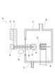
- FIG. 2 shows a microwave-excited plasma CVD (Microwave Plasma Chemical Vapor Deposition, hereinafter referred to as MPCVD) apparatus 10.
- MPCVD Microwave Plasma Chemical Vapor Deposition
- the chamber 11 and the object S are placed, and the DC voltage applicable sample stage 12 (hereinafter referred to as stage 12), the magnetron generator 13 that generates microwaves, and the waveguide converter 14 , A waveguide 15, a temperature measuring device 16, a raw material gas supply path 17, a raw material gas exhaust path 18, an induction heating coil 19, and an antenna electrode 20.
- stage 12 the DC voltage applicable sample stage 12
- the magnetron generator 13 that generates microwaves
- the waveguide converter 14 A waveguide 15, a temperature measuring device 16, a raw material gas supply path 17, a raw material gas exhaust path 18, an induction heating coil 19, and an antenna electrode 20.
- the object S has a ruthenium film 3 formed on the surface of the sapphire base material 2.
- the object S is fixed on the stage 12 with a clamp ring or the like in a direction in which the surface of the ruthenium film 3 faces upward, and is heated to a predetermined temperature by an induction heating coil 19 provided on the stage 12.
- the temperature of the object S fixed on the stage 12 is monitored by the non-contact temperature measuring device 16.
- a raw material gas containing hydrogen and methane is supplied into the chamber 11 from the raw material gas supply path 17, and microwaves are transmitted from the magnetron generator 13, so that a plasma ball 21 is generated near the tip of the antenna electrode 20.
- the plasma ball 21 is held near the tip of the antenna electrode 20 without moving during the process.
- diamond grows heteroepitaxially on the surface of the ruthenium film 3 using carbon in the raw material gas as a raw material, and a diamond film 4 having a (111) surface as the surface is formed.
- the ruthenium atom Ru has a six-fold symmetric arrangement on the same plane on the ruthenium (0001) plane which is the upper surface of the hexagonal structure.
- the carbon atom C has a six-fold symmetric arrangement on the same plane as the ruthenium atom Ru on the diamond (111) plane. Due to such an atomic arrangement, the diamond (111) plane can be heteroepitaxially grown on the ruthenium (0001) plane.
- the diamond [111] crystal orientation and the ruthenium [0001] crystal orientation are parallel in the direction perpendicular to the substrate plane, and the diamond [11-2] crystal orientation in the direction parallel to the substrate plane.
- the ruthenium [10-10] crystal orientations are parallel. Since diamond is a cubic crystal and ruthenium is a hexagonal crystal, it is not possible to simply obtain the lattice mismatch rate from each lattice constant. However, since the diamond (111) plane and the ruthenium (0001) plane each have a six-fold symmetric atomic arrangement on the same plane as described above, the lattice mismatch rate can be obtained.
- the lattice mismatch rate between the diamond (111) plane and the ruthenium (0001) plane is 7.0%, which is the lattice mismatch rate between the diamond (111) plane and the iridium (111) plane, 7.1%. Therefore, a single crystal diamond substrate 1 on which the diamond film 4 having higher quality crystallinity is formed can be obtained.
- the single crystal diamond substrate 1 of the embodiment has a diamond film 4 which is a heteroepitaxial film formed on the ruthenium film 3, and is a laminate and a single crystal of the ruthenium film 3 and the diamond film 4 having such a configuration. No diamond substrate has been reported so far.
- the diamond (111) plane single crystal diamond substrate has higher industrial utility value.
- the (0001) surface of the ruthenium film 3 is used as a base film, and the (111) surface of the diamond film 4 is heteroepitaxially grown.
- Platinum and iridium are cubic, while ruthenium is hexagonal.
- the hexagonal (0001) plane having a 6-fold symmetric atomic arrangement on the same plane is perpendicular to the plane (both the film thickness direction and the C-axis direction) than the (111) plane of the cubic crystal having the same atomic arrangement. (Called) has the characteristic of being easy to grow crystals.
- ruthenium which is a hexagonal crystal
- platinum and iridium which are cubic crystals
- a (111) -plane single crystal diamond substrate having higher crystallinity can be obtained.
- ruthenium is cheaper than platinum and iridium, it is possible to obtain a (111) -plane single crystal diamond substrate at a lower cost than when platinum or iridium is used as a base film.
- the laminated body is not limited to the single crystal diamond substrate, and a diamond film which is an epitaxial film and whose surface is the (111) plane is laminated on the ruthenium film. Anything may be used as long as it has a laminated structure.
- the sapphire base material 2 was a single crystal C-plane sapphire (Al 2 O 3, (0001) plane) having a thickness of 500 ⁇ m.
- the thickness of the ruthenium film 3 was set to 150 nm.
- a ruthenium film 3 oriented to the (0001) plane was formed on the surface of the sapphire substrate 2 by a sputtering method to a thickness of 150 nm.
- the sputtering temperature was 600 ° C.
- the diamond film 4 was formed by heteroepitaxial growth on the ruthenium film 3 by the plasma CVD method.
- the heteroepitaxial growth of the diamond film 4 was carried out in two steps: nucleation on the ruthenium film 3 followed by epitaxial growth of the (111) plane.
- the maximum thickness of the diamond film 4 was 200 nm.
- Nucleation was performed by the BEN (Bias Enhanced Nucleation) process. Specifically, in the MPCVD apparatus 10, the plasma was discharged for 30 seconds by applying a bias of ⁇ 150 V in an atmosphere where the temperature was 650 ° C., hydrogen was 90%, and methane was 10%.
- BEN Bias Enhanced Nucleation
- the heteroepitaxial growth of the (111) plane which was carried out following the nucleation, was carried out by discharging the plasma for 30 minutes in an atmosphere where the temperature was 600 ° C., hydrogen was 99.7%, and methane was 0.3%. ..
- a laminated body of the ruthenium film 3 and the diamond film 4 was produced.
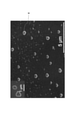
- the surface of the prepared laminate of ruthenium film 3 and diamond film 4 was observed by SEM (scanning electron microscope). As shown in FIG. 4, a diamond film 4 was formed on the ruthenium film 3, and some crystal grains of the diamond film 4 showed a substantially hexagonal contour shape (pseudo-hexagon). This indicates that the diamond film 4 has grown laterally.
- the average diameter of the diamond film 4 was about 500 nm. Since the crystal grain size of the diamond film 4 can be further increased by appropriately adjusting the process conditions for heteroepitaxial growth, a single crystal diamond is formed by forming the diamond film 4 so as to cover the entire surface of the ruthenium film 3. It is considered that the substrate 1 can be obtained.
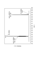
- FIG. 5 shows the results of performing a 2 ⁇ scan of X-ray diffraction on the sample of the second example.
- the X-ray diffraction patterns are 42.2 ° and 92.0 ° corresponding to the Ru (0002) plane and the Ru (0004) plane of the ruthenium film 3, respectively, and Al 2 of the sapphire substrate 2.
- Diffraction peaks were shown at 41.7 ° and 90.7 ° corresponding to the O 3 (0006) plane and the Al 2 O 3 (00012) plane, respectively.
- no diffraction peak corresponding to the crystal planes other than the (0002) plane and the (0004) plane, which are the planes equivalent to the (0001) plane of ruthenium was detected.
- the ruthenium film 3 formed on the sapphire substrate 2 was a single crystal.
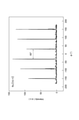
- FIG. 6 shows the results of performing a ⁇ scan of X-ray diffraction on the sample of the second example.
- six reflection peaks on the equivalent ⁇ 10-11 ⁇ plane of the ⁇ scan were detected in a 60 ° cycle. These reflected peaks correspond to the 6-fold symmetric structure (see FIG. 3) of the ruthenium (0001) plane, which is the upper surface of the hexagonal crystal described in the embodiment.
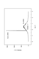
- FIG. 7 shows the results of performing an ⁇ scan (locking curve measurement) of X-ray diffraction on the sample of the second example. It was confirmed that the full width at half maximum (FWHM) of the locking curve of the Ru (0002) plane was 1.1 °.
- the laminate of the ruthenium film 3 and the diamond film 4 produced by the same procedure as in the first embodiment was analyzed by the EBSD (Electron Back Scattered Diffraction) method. ..
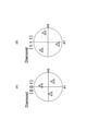
- FIG. 8 and 9 are pole figures in the ND direction (normal direction) analyzed by the EBSD method.
- FIG. 8A is a pole figure of the diamond ⁇ 001 ⁇ plane
- FIG. 8B is a pole figure of the diamond ⁇ 111 ⁇ plane.
- 9 (A) is a pole figure of the diamond ⁇ 011 ⁇ plane
- FIG. 9 (B) is a pole figure of the diamond ⁇ 211 ⁇ plane
- FIG. 9 (C) is a pole figure of the ruthenium ⁇ 11-20 ⁇ plane.
- FIG. 9D is an extreme point view of the ruthenium ⁇ 10-10 ⁇ plane.
- the pole figures shown in FIGS. 9 (A) to 9 (D) were all acquired at the same time in order to specify the direction of epitaxial growth.
- the reflection on the diamond ⁇ 011 ⁇ surface was strongly detected at the six positions surrounded by ⁇ on the outermost circumference.
- the reflection on the diamond ⁇ 211 ⁇ plane was strongly detected at the five positions circled on the outermost circumference.
- FIG. 9 (A) Six positions surrounded by ⁇ where reflections on the diamond ⁇ 011 ⁇ surface were strongly detected (Fig. 9 (A)) and six positions surrounded by ⁇ where reflections on the ruthenium ⁇ 11-20 ⁇ surface were strongly detected (Fig. 9 (A)).
- FIG. 9C) was located at the corresponding position on the pole figure.
- the five positions circled with strong reflections on the diamond ⁇ 211 ⁇ surface (FIG. 9 (B)) and the six circled circles with strong ruthenium ⁇ 10-10 ⁇ surface reflections were detected.
- Five of the positions (FIG. 9 (D)) were located at corresponding locations on the pole map.
- crystal planes of the six ⁇ 11-20 ⁇ column planes equivalent in the hexagonal structure with the 6-fold symmetry structure of the ruthenium (0001) plane as the upper surface and their orientations are 6 of the diamond (111) plane. It is shown that they are parallel to the crystal planes of six equivalent ⁇ 011 ⁇ planes, which are the pillar planes in the hexagonal column structure having the rotationally symmetric structure as the upper surface, and the orientations are the same. It shows that a similar relationship holds for the six equivalent ⁇ 10-10 ⁇ planes of ruthenium and the six equivalent ⁇ 211 ⁇ planes of diamond.
- the analysis result by the EBSD method of Example 3 shows that the diamond [111] crystal orientation and the ruthenium [0001] crystal orientation are the crystal orientations of the diamond film 4 and the ruthenium film 3 of the laminated body of the prepared ruthenium film 3 and the diamond film 4. It is shown that they match and that the diamond [11-2] crystal orientation and the ruthenium [10-10] crystal orientation match, and it is confirmed that the diamond film 4 is heteroepitaxially grown on the ruthenium film 3. I was able to.
Landscapes
- Chemical & Material Sciences (AREA)
- Organic Chemistry (AREA)
- Engineering & Computer Science (AREA)
- Materials Engineering (AREA)
- Metallurgy (AREA)
- Crystallography & Structural Chemistry (AREA)
- Chemical Kinetics & Catalysis (AREA)
- General Chemical & Material Sciences (AREA)
- Inorganic Chemistry (AREA)
- Life Sciences & Earth Sciences (AREA)
- Geology (AREA)
- General Life Sciences & Earth Sciences (AREA)
- Mechanical Engineering (AREA)
- Crystals, And After-Treatments Of Crystals (AREA)
- Laminated Bodies (AREA)
- Carbon And Carbon Compounds (AREA)
- Chemical Vapour Deposition (AREA)
Priority Applications (1)
| Application Number | Priority Date | Filing Date | Title |
|---|---|---|---|
| US18/042,725 US12378691B2 (en) | 2020-08-26 | 2021-08-19 | Laminate, single crystal diamond substrate and method of producing same |
Applications Claiming Priority (2)
| Application Number | Priority Date | Filing Date | Title |
|---|---|---|---|
| JP2020-143009 | 2020-08-26 | ||
| JP2020143009A JP7569527B2 (ja) | 2020-08-26 | 2020-08-26 | 積層体、単結晶ダイヤモンド基板及びその製造方法 |
Publications (1)
| Publication Number | Publication Date |
|---|---|
| WO2022044946A1 true WO2022044946A1 (ja) | 2022-03-03 |
Family
ID=80355162
Family Applications (1)
| Application Number | Title | Priority Date | Filing Date |
|---|---|---|---|
| PCT/JP2021/030346 Ceased WO2022044946A1 (ja) | 2020-08-26 | 2021-08-19 | 積層体、単結晶ダイヤモンド基板及びその製造方法 |
Country Status (4)
| Country | Link |
|---|---|
| US (1) | US12378691B2 (enExample) |
| JP (1) | JP7569527B2 (enExample) |
| TW (1) | TWI905253B (enExample) |
| WO (1) | WO2022044946A1 (enExample) |
Families Citing this family (1)
| Publication number | Priority date | Publication date | Assignee | Title |
|---|---|---|---|---|
| US20260132542A1 (en) * | 2024-06-03 | 2026-05-14 | Tech University Of Korea Industry Academic Cooperation Foundation | Single-crystal diamond substrate with twin defects removed and method for manufacturing the same |
Citations (6)
| Publication number | Priority date | Publication date | Assignee | Title |
|---|---|---|---|---|
| JPH06212428A (ja) * | 1993-01-20 | 1994-08-02 | Matsufumi Takatani | 金属表面へのダイヤモンド被覆の形成方法 |
| JP2005219962A (ja) * | 2004-02-05 | 2005-08-18 | Sumitomo Electric Ind Ltd | ダイヤモンド単結晶基板及びその製造方法 |
| US20070084398A1 (en) * | 2003-05-06 | 2007-04-19 | Universitat Augsburg | Monocrystalline diamond layer and method for the production thereof |
| US20160208413A1 (en) * | 2015-01-19 | 2016-07-21 | Fraunhofer-Gesellschaft zur Förderung der angewandten Forschung e.V. | Epitaxial diamond layer and method for the production thereof |
| JP2016145144A (ja) * | 2015-01-28 | 2016-08-12 | パナソニックIpマネジメント株式会社 | ダイヤモンド積層構造、ダイヤモンド半導体形成用基板、ダイヤモンド半導体装置およびダイヤモンド積層構造の製造方法 |
| JP2020090408A (ja) * | 2018-12-04 | 2020-06-11 | 信越化学工業株式会社 | 積層基板、自立基板、積層基板の製造方法及び自立基板の製造方法 |
Family Cites Families (3)
| Publication number | Priority date | Publication date | Assignee | Title |
|---|---|---|---|---|
| US6201342B1 (en) * | 1997-06-30 | 2001-03-13 | The United States Of America As Represented By The Secretary Of The Navy | Automatically sharp field emission cathodes |
| TW522504B (en) * | 2001-02-15 | 2003-03-01 | Ngk Insulators Ltd | Diamond-coated member |
| EP2801551A1 (en) * | 2013-05-08 | 2014-11-12 | Max-Planck-Gesellschaft zur Förderung der Wissenschaften e.V. | Graphene with very high charge carrier mobility and preparation thereof |
-
2020
- 2020-08-26 JP JP2020143009A patent/JP7569527B2/ja active Active
-
2021
- 2021-08-19 WO PCT/JP2021/030346 patent/WO2022044946A1/ja not_active Ceased
- 2021-08-19 US US18/042,725 patent/US12378691B2/en active Active
- 2021-08-25 TW TW110131420A patent/TWI905253B/zh active
Patent Citations (6)
| Publication number | Priority date | Publication date | Assignee | Title |
|---|---|---|---|---|
| JPH06212428A (ja) * | 1993-01-20 | 1994-08-02 | Matsufumi Takatani | 金属表面へのダイヤモンド被覆の形成方法 |
| US20070084398A1 (en) * | 2003-05-06 | 2007-04-19 | Universitat Augsburg | Monocrystalline diamond layer and method for the production thereof |
| JP2005219962A (ja) * | 2004-02-05 | 2005-08-18 | Sumitomo Electric Ind Ltd | ダイヤモンド単結晶基板及びその製造方法 |
| US20160208413A1 (en) * | 2015-01-19 | 2016-07-21 | Fraunhofer-Gesellschaft zur Förderung der angewandten Forschung e.V. | Epitaxial diamond layer and method for the production thereof |
| JP2016145144A (ja) * | 2015-01-28 | 2016-08-12 | パナソニックIpマネジメント株式会社 | ダイヤモンド積層構造、ダイヤモンド半導体形成用基板、ダイヤモンド半導体装置およびダイヤモンド積層構造の製造方法 |
| JP2020090408A (ja) * | 2018-12-04 | 2020-06-11 | 信越化学工業株式会社 | 積層基板、自立基板、積層基板の製造方法及び自立基板の製造方法 |
Non-Patent Citations (1)
| Title |
|---|
| FEI, WENXI ET AL.: "Local initial heteroepitaxial growth of diamond(l 11) on Ru(0001)/c-sapphire by antenna-edge-type microwave plasma chemical vapor deposition", APPLIED PHYSICS LETTERS, vol. 117, no. 11, 18 September 2020 (2020-09-18), XP012250155, DOI: 10.1063/5.0008287 * |
Also Published As
| Publication number | Publication date |
|---|---|
| US20230349070A1 (en) | 2023-11-02 |
| TWI905253B (zh) | 2025-11-21 |
| US12378691B2 (en) | 2025-08-05 |
| TW202219301A (zh) | 2022-05-16 |
| JP7569527B2 (ja) | 2024-10-18 |
| JP2022038478A (ja) | 2022-03-10 |
Similar Documents
| Publication | Publication Date | Title |
|---|---|---|
| TWI787234B (zh) | 鑽石成膜用基底基板、以及使用其之鑽石基板的製造方法 | |
| US9200379B2 (en) | Base material for growing single crystal diamond and method for producing single crystal diamond substrate | |
| JP6112485B2 (ja) | 単結晶ダイヤモンドの製造方法 | |
| JP7475389B2 (ja) | 積層基板、積層基板の製造方法及び自立基板の製造方法 | |
| US20110081531A1 (en) | Base material for growing single crystal diamond and method for producing single crystal diamond substrate | |
| US7628856B2 (en) | Method for producing substrate for single crystal diamond growth | |
| JPH11147794A (ja) | 単結晶SiC及びその製造方法 | |
| JP4528654B2 (ja) | 積層基板、積層基板の製造方法及びデバイス | |
| JP7017299B2 (ja) | ダイヤモンド電子素子及びダイヤモンド電子素子の製造方法 | |
| US20240279842A1 (en) | Diamond substrate and method for manufacturing same | |
| JP7569527B2 (ja) | 積層体、単結晶ダイヤモンド基板及びその製造方法 | |
| JP2025175289A (ja) | 下地基板及び単結晶ダイヤモンド積層基板並びにそれらの製造方法 | |
| US20250154685A1 (en) | Underlying substrate, single crystal diamond laminate substrate and method for producing them | |
| JP2022109306A (ja) | ダイヤモンド製膜用下地基板及びそれを用いたダイヤモンド基板の製造方法 | |
| US20260068551A1 (en) | Underlying substrate, single crystal diamond laminate substrate and method for producing them | |
| TW202528572A (zh) | 鑽石基板及其製造方法以及感測器 | |
| JP2017226573A (ja) | 積層基板の製造方法および積層基板 | |
| JPH09309795A (ja) | 立方晶窒化アルミニウム薄膜およびその合成方法 |
Legal Events
| Date | Code | Title | Description |
|---|---|---|---|
| 121 | Ep: the epo has been informed by wipo that ep was designated in this application |
Ref document number: 21861374 Country of ref document: EP Kind code of ref document: A1 |
|
| DPE1 | Request for preliminary examination filed after expiration of 19th month from priority date (pct application filed from 20040101) | ||
| NENP | Non-entry into the national phase |
Ref country code: DE |
|
| 122 | Ep: pct application non-entry in european phase |
Ref document number: 21861374 Country of ref document: EP Kind code of ref document: A1 |
|
| WWG | Wipo information: grant in national office |
Ref document number: 18042725 Country of ref document: US |