WO2022044865A1 - 半導体発光装置及び光源装置 - Google Patents
半導体発光装置及び光源装置 Download PDFInfo
- Publication number
- WO2022044865A1 WO2022044865A1 PCT/JP2021/029884 JP2021029884W WO2022044865A1 WO 2022044865 A1 WO2022044865 A1 WO 2022044865A1 JP 2021029884 W JP2021029884 W JP 2021029884W WO 2022044865 A1 WO2022044865 A1 WO 2022044865A1
- Authority
- WO
- WIPO (PCT)
- Prior art keywords
- light emitting
- semiconductor light
- emitting device
- metal layer
- wiring board
- Prior art date
- Legal status (The legal status is an assumption and is not a legal conclusion. Google has not performed a legal analysis and makes no representation as to the accuracy of the status listed.)
- Ceased
Links
Images




















Classifications
-
- H—ELECTRICITY
- H01—ELECTRIC ELEMENTS
- H01S—DEVICES USING THE PROCESS OF LIGHT AMPLIFICATION BY STIMULATED EMISSION OF RADIATION [LASER] TO AMPLIFY OR GENERATE LIGHT; DEVICES USING STIMULATED EMISSION OF ELECTROMAGNETIC RADIATION IN WAVE RANGES OTHER THAN OPTICAL
- H01S5/00—Semiconductor lasers
- H01S5/02—Structural details or components not essential to laser action
- H01S5/022—Mountings; Housings
- H01S5/0225—Out-coupling of light
- H01S5/02257—Out-coupling of light using windows, e.g. specially adapted for back-reflecting light to a detector inside the housing
-
- H—ELECTRICITY
- H01—ELECTRIC ELEMENTS
- H01S—DEVICES USING THE PROCESS OF LIGHT AMPLIFICATION BY STIMULATED EMISSION OF RADIATION [LASER] TO AMPLIFY OR GENERATE LIGHT; DEVICES USING STIMULATED EMISSION OF ELECTROMAGNETIC RADIATION IN WAVE RANGES OTHER THAN OPTICAL
- H01S5/00—Semiconductor lasers
- H01S5/005—Optical components external to the laser cavity, specially adapted therefor, e.g. for homogenisation or merging of the beams or for manipulating laser pulses, e.g. pulse shaping
- H01S5/0064—Anti-reflection components, e.g. optical isolators
-
- H—ELECTRICITY
- H01—ELECTRIC ELEMENTS
- H01S—DEVICES USING THE PROCESS OF LIGHT AMPLIFICATION BY STIMULATED EMISSION OF RADIATION [LASER] TO AMPLIFY OR GENERATE LIGHT; DEVICES USING STIMULATED EMISSION OF ELECTROMAGNETIC RADIATION IN WAVE RANGES OTHER THAN OPTICAL
- H01S5/00—Semiconductor lasers
- H01S5/005—Optical components external to the laser cavity, specially adapted therefor, e.g. for homogenisation or merging of the beams or for manipulating laser pulses, e.g. pulse shaping
- H01S5/0071—Optical components external to the laser cavity, specially adapted therefor, e.g. for homogenisation or merging of the beams or for manipulating laser pulses, e.g. pulse shaping for beam steering, e.g. using a mirror outside the cavity to change the beam direction
-
- H—ELECTRICITY
- H01—ELECTRIC ELEMENTS
- H01S—DEVICES USING THE PROCESS OF LIGHT AMPLIFICATION BY STIMULATED EMISSION OF RADIATION [LASER] TO AMPLIFY OR GENERATE LIGHT; DEVICES USING STIMULATED EMISSION OF ELECTROMAGNETIC RADIATION IN WAVE RANGES OTHER THAN OPTICAL
- H01S5/00—Semiconductor lasers
- H01S5/02—Structural details or components not essential to laser action
- H01S5/022—Mountings; Housings
- H01S5/02208—Mountings; Housings characterised by the shape of the housings
-
- H—ELECTRICITY
- H01—ELECTRIC ELEMENTS
- H01S—DEVICES USING THE PROCESS OF LIGHT AMPLIFICATION BY STIMULATED EMISSION OF RADIATION [LASER] TO AMPLIFY OR GENERATE LIGHT; DEVICES USING STIMULATED EMISSION OF ELECTROMAGNETIC RADIATION IN WAVE RANGES OTHER THAN OPTICAL
- H01S5/00—Semiconductor lasers
- H01S5/02—Structural details or components not essential to laser action
- H01S5/022—Mountings; Housings
- H01S5/02218—Material of the housings; Filling of the housings
-
- H—ELECTRICITY
- H01—ELECTRIC ELEMENTS
- H01S—DEVICES USING THE PROCESS OF LIGHT AMPLIFICATION BY STIMULATED EMISSION OF RADIATION [LASER] TO AMPLIFY OR GENERATE LIGHT; DEVICES USING STIMULATED EMISSION OF ELECTROMAGNETIC RADIATION IN WAVE RANGES OTHER THAN OPTICAL
- H01S5/00—Semiconductor lasers
- H01S5/02—Structural details or components not essential to laser action
- H01S5/022—Mountings; Housings
- H01S5/023—Mount members, e.g. sub-mount members
-
- H—ELECTRICITY
- H01—ELECTRIC ELEMENTS
- H01S—DEVICES USING THE PROCESS OF LIGHT AMPLIFICATION BY STIMULATED EMISSION OF RADIATION [LASER] TO AMPLIFY OR GENERATE LIGHT; DEVICES USING STIMULATED EMISSION OF ELECTROMAGNETIC RADIATION IN WAVE RANGES OTHER THAN OPTICAL
- H01S5/00—Semiconductor lasers
- H01S5/02—Structural details or components not essential to laser action
- H01S5/022—Mountings; Housings
- H01S5/0233—Mounting configuration of laser chips
- H01S5/02345—Wire-bonding
-
- H—ELECTRICITY
- H01—ELECTRIC ELEMENTS
- H01S—DEVICES USING THE PROCESS OF LIGHT AMPLIFICATION BY STIMULATED EMISSION OF RADIATION [LASER] TO AMPLIFY OR GENERATE LIGHT; DEVICES USING STIMULATED EMISSION OF ELECTROMAGNETIC RADIATION IN WAVE RANGES OTHER THAN OPTICAL
- H01S5/00—Semiconductor lasers
- H01S5/02—Structural details or components not essential to laser action
- H01S5/024—Arrangements for thermal management
- H01S5/02461—Structure or details of the laser chip to manipulate the heat flow, e.g. passive layers in the chip with a low heat conductivity
-
- H—ELECTRICITY
- H01—ELECTRIC ELEMENTS
- H01S—DEVICES USING THE PROCESS OF LIGHT AMPLIFICATION BY STIMULATED EMISSION OF RADIATION [LASER] TO AMPLIFY OR GENERATE LIGHT; DEVICES USING STIMULATED EMISSION OF ELECTROMAGNETIC RADIATION IN WAVE RANGES OTHER THAN OPTICAL
- H01S5/00—Semiconductor lasers
- H01S5/02—Structural details or components not essential to laser action
- H01S5/024—Arrangements for thermal management
- H01S5/02469—Passive cooling, e.g. where heat is removed by the housing as a whole or by a heat pipe without any active cooling element like a TEC
-
- H—ELECTRICITY
- H01—ELECTRIC ELEMENTS
- H01S—DEVICES USING THE PROCESS OF LIGHT AMPLIFICATION BY STIMULATED EMISSION OF RADIATION [LASER] TO AMPLIFY OR GENERATE LIGHT; DEVICES USING STIMULATED EMISSION OF ELECTROMAGNETIC RADIATION IN WAVE RANGES OTHER THAN OPTICAL
- H01S5/00—Semiconductor lasers
- H01S5/02—Structural details or components not essential to laser action
- H01S5/022—Mountings; Housings
- H01S5/023—Mount members, e.g. sub-mount members
- H01S5/02315—Support members, e.g. bases or carriers
-
- H—ELECTRICITY
- H01—ELECTRIC ELEMENTS
- H01S—DEVICES USING THE PROCESS OF LIGHT AMPLIFICATION BY STIMULATED EMISSION OF RADIATION [LASER] TO AMPLIFY OR GENERATE LIGHT; DEVICES USING STIMULATED EMISSION OF ELECTROMAGNETIC RADIATION IN WAVE RANGES OTHER THAN OPTICAL
- H01S5/00—Semiconductor lasers
- H01S5/02—Structural details or components not essential to laser action
- H01S5/022—Mountings; Housings
- H01S5/0233—Mounting configuration of laser chips
- H01S5/0234—Up-side down mountings, e.g. Flip-chip, epi-side down mountings or junction down mountings
-
- H—ELECTRICITY
- H01—ELECTRIC ELEMENTS
- H01S—DEVICES USING THE PROCESS OF LIGHT AMPLIFICATION BY STIMULATED EMISSION OF RADIATION [LASER] TO AMPLIFY OR GENERATE LIGHT; DEVICES USING STIMULATED EMISSION OF ELECTROMAGNETIC RADIATION IN WAVE RANGES OTHER THAN OPTICAL
- H01S5/00—Semiconductor lasers
- H01S5/02—Structural details or components not essential to laser action
- H01S5/022—Mountings; Housings
- H01S5/0235—Method for mounting laser chips
- H01S5/02355—Fixing laser chips on mounts
- H01S5/0237—Fixing laser chips on mounts by soldering
-
- H—ELECTRICITY
- H01—ELECTRIC ELEMENTS
- H01S—DEVICES USING THE PROCESS OF LIGHT AMPLIFICATION BY STIMULATED EMISSION OF RADIATION [LASER] TO AMPLIFY OR GENERATE LIGHT; DEVICES USING STIMULATED EMISSION OF ELECTROMAGNETIC RADIATION IN WAVE RANGES OTHER THAN OPTICAL
- H01S5/00—Semiconductor lasers
- H01S5/02—Structural details or components not essential to laser action
- H01S5/022—Mountings; Housings
- H01S5/0239—Combinations of electrical or optical elements
Definitions
- This disclosure relates to a semiconductor light emitting device and a light source device.
- a semiconductor light emitting device in which a semiconductor light emitting element such as a semiconductor laser element is mounted on a substrate and the semiconductor light emitting element is covered with a cap has been proposed (see, for example, Patent Documents 1 and 2).
- Patent Documents 1 and 2 propose a structure in which a semiconductor laser element is mounted on a substrate via a submount and a cap for covering the semiconductor laser element is arranged on the substrate. A transparent plate for extracting laser light is arranged on the side surface of the cap.
- the present disclosure has been made to solve such a problem, and an object of the present invention is to provide a semiconductor light emitting device having a simplified configuration and capable of realizing high light output and reliability improvement of a semiconductor light emitting device. And.
- one aspect of the semiconductor light emitting device is a wiring board, a semiconductor light emitting element arranged on the upper surface of the wiring board, and the semiconductor light emitting device arranged on the upper surface of the wiring board.
- a cap unit for covering the element is provided, and the wiring board is arranged on the first board, a first metal layer and a second metal layer arranged apart from each other on the first board, and the first board.
- the bonding surface of the cap unit to be joined to the wiring board intersects the first metal layer and the second metal layer in the top view of the wiring board, and the spacer layer is formed by the spacer layer. It is arranged at a position different from that of the first metal layer and the second metal layer between the joint surface and the first substrate.
- the wiring board further has a first insulating layer arranged on the upper surface of the first board, and the first metal layer, the second metal layer, and the like. And the spacer layer may be arranged on the first insulating layer.
- the first substrate may be a metal substrate.
- the metal substrate may be made of a metal flat plate.
- an opening may be formed in the first insulating layer, and the semiconductor light emitting device may be arranged in the opening.
- the spacer layer may be arranged along the bonding surface.
- the wiring board may have the first metal layer, the second metal layer, and the second insulating layer covering at least a part of the spacer layer. good.
- the spacer layer may be made of a metal material.
- the spacer layer is made of the same material as the first metal layer or the second metal layer, and is the same as the first metal layer or the second metal layer. It may be electrically connected.
- the cap unit has a rectangular top plate and four side walls connected to four sides of the peripheral edge of the top plate, respectively, and the four side walls of the four side walls.
- One of them is a translucent window having an inorganic translucent plate and an antireflection film arranged on the inorganic translucent plate, and light emitted from the semiconductor light emitting device is transmitted through the translucent window. You may.
- the top plate may be transparent.
- the distance between the translucent window and the emission surface of the semiconductor light emitting device may be larger than zero and less than the thickness of the translucent window.
- the thickness of the side wall other than the translucent window among the four side walls may be larger than the thickness of the transmissive window.
- the cap unit has a rectangular top plate and four side walls connected to four sides of the peripheral edge of the top plate, and the top plate has four side walls. It is a translucent window having an inorganic translucent plate and an antireflection film formed on the inorganic translucent plate, and light emitted from the semiconductor light emitting device may pass through the translucent window.
- the semiconductor light emitting device includes a reflective optical element, and light emitted from the semiconductor light emitting element is reflected by the reflected optical element and is applied to the upper surface of the wiring substrate. It may propagate in the vertical direction.
- one aspect of the semiconductor light emitting device may include a functional element arranged on the wiring board.
- the functional element may be covered with the cap unit.
- the functional element may be a temperature detecting element.
- the temperature detecting element may be arranged at a position that does not intersect with the optical axis of the semiconductor light emitting device.
- one aspect of the semiconductor light emitting device may further include a shielding member arranged between the temperature detecting element and the semiconductor light emitting device.
- an oblique cut surface may be provided at the end of the first substrate.
- one aspect of the light source device is a semiconductor light emitting device, a heat sink in which the semiconductor light emitting device is arranged, and a fixing screw for fixing the semiconductor light emitting device to the heat sink.
- the wiring board is formed with a through hole, and the fixing screw penetrates the through hole and is fixed to the heat sink.
- one aspect of the light source device includes a cable having terminals and a terminal fixing screw, and the wiring board has a take-out electrode electrically connected to the first metal layer.
- An electrode through hole is formed in the center of the take-out electrode, the terminal fixing screw penetrates the electrode through hole, and the terminal is arranged between the terminal fixing screw and the take-out electrode to form a take-out electrode.
- the terminal may be electrically connected.
- FIG. 1A is a schematic perspective view showing the overall configuration of the semiconductor light emitting device according to the first embodiment.
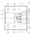
- FIG. 1B is a schematic top view showing the overall configuration of the semiconductor light emitting device according to the first embodiment.
- FIG. 2 is a schematic perspective view showing the internal configuration of the cap unit of the semiconductor light emitting device according to the first embodiment.
- FIG. 3A is a schematic exploded perspective view illustrating the overall configuration of the semiconductor light emitting device according to the first embodiment.
- FIG. 3B is an equivalent circuit for explaining the circuit configuration of the semiconductor light emitting device according to the first embodiment.
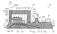
- FIG. 4 is a schematic cross-sectional view illustrating the overall configuration of the semiconductor light emitting device according to the first embodiment.
- FIG. 5 is a schematic top view showing the positional relationship between the semiconductor light emitting device, each metal layer, and each spacer layer of the semiconductor light emitting device according to the first embodiment and the joint surface of the cap unit.
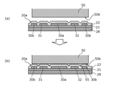
- FIG. 6A is a schematic cross-sectional view showing a bonding state between the wiring board according to the comparative example and the cap unit.
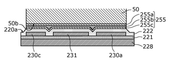
- FIG. 6B is a schematic cross-sectional view showing a bonding state between the wiring board according to the first embodiment and the cap unit.
- FIG. 7 is a schematic diagram illustrating each dimension of the first metal layer according to the first embodiment.
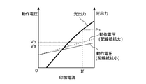
- FIG. 8 is a graph showing the relationship between the applied current of the semiconductor light emitting device according to the first embodiment, the operating voltage, and the optical output.
- FIG. 10A is a schematic cross-sectional view illustrating the first step of the method for manufacturing a wiring board according to the first embodiment.
- FIG. 10B is a schematic cross-sectional view illustrating a second step of the method for manufacturing a wiring board according to the first embodiment.
- FIG. 10C is a schematic cross-sectional view illustrating a third step of the method for manufacturing a wiring board according to the first embodiment.
- FIG. 10D is a schematic cross-sectional view illustrating a fourth step of the method for manufacturing a wiring board according to the first embodiment.
- FIG. 10E is a schematic cross-sectional view illustrating a fifth step of the method for manufacturing a wiring board according to the first embodiment.
- FIG. 10F is a schematic cross-sectional view illustrating a sixth step of the method for manufacturing a wiring board according to the first embodiment.
- FIG. 10G is a schematic cross-sectional view illustrating a seventh step of the method for manufacturing a wiring board according to the first embodiment.
- FIG. 11 is a schematic perspective view illustrating a method of manufacturing a cap unit according to the first embodiment.
- FIG. 12A is a schematic cross-sectional view illustrating a method of attaching the cap unit according to the first embodiment to the wiring board.
- FIG. 12B is a schematic cross-sectional view of a light source device using the semiconductor light emitting device according to the first embodiment.
- FIG. 13A is a schematic top view showing the configuration of each spacer layer of the semiconductor light emitting device according to the first modification of the first embodiment.
- FIG. 13B is a schematic top view showing the configuration of each spacer layer of the semiconductor light emitting device according to the second modification of the first embodiment.
- FIG. 14A is a schematic top view showing the positional relationship between the semiconductor light emitting device, the temperature detecting element, and the shielding member of the semiconductor light emitting device according to the third modification of the first embodiment.
- FIG. 14B is a schematic cross-sectional view showing the positional relationship between the semiconductor light emitting device, the temperature detecting element, and the shielding member of the semiconductor light emitting device according to the third modification of the first embodiment.
- FIG. 14A is a schematic top view showing the positional relationship between the semiconductor light emitting device, the temperature detecting element, and the shielding member of the semiconductor light emitting device according to the third modification of the first embodiment.
- FIG. 15 is a schematic perspective view showing the overall configuration of the semiconductor light emitting device according to the second embodiment.
- FIG. 16 is a schematic perspective view showing the overall configuration of the semiconductor light emitting device according to the second embodiment.
- FIG. 17 is a schematic cross-sectional view showing the overall configuration of the semiconductor light emitting device according to the second embodiment.
- FIG. 18 is a top view showing the arrangement of the temperature detecting element according to the second embodiment.
- FIG. 19A is a schematic first cross-sectional view illustrating a method of joining the cap unit of the semiconductor light emitting device according to the second embodiment to the wiring board.
- FIG. 19B is a schematic second sectional view illustrating a method of joining the cap unit of the semiconductor light emitting device according to the second embodiment to the wiring board.
- FIG. 19C is a schematic third sectional view illustrating a method of joining the cap unit of the semiconductor light emitting device according to the second embodiment to the wiring board.
- FIG. 20 is a schematic perspective view showing the configuration of the light source device according to the second embodiment.
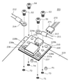
- FIG. 21 is a schematic exploded perspective view showing the configuration of the light source device according to the second embodiment.
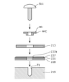
- FIG. 22A is a schematic cross-sectional view showing a state in which the terminal fixing screw according to the first modification of the second embodiment is fixed to the heat sink.
- FIG. 22B is an exploded cross-sectional view showing a method of fixing the terminal fixing screw to the heat sink according to the first modification of the second embodiment.
- FIG. 23 is a schematic perspective view showing the overall configuration of the semiconductor light emitting device according to the third embodiment.
- FIG. 24 is a schematic exploded perspective view showing the overall configuration of the semiconductor light emitting device according to the third embodiment.
- FIG. 25 is a schematic cross-sectional view showing the overall configuration of the semiconductor light emitting device according to the third embodiment.
- FIG. 26 is a schematic top view showing the overall configuration of the semiconductor light emitting device according to the modified example of the third embodiment.
- FIG. 27 is a schematic top view showing the overall configuration of the semiconductor light emitting device according to the fourth embodiment.
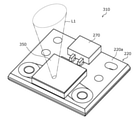
- FIG. 28 is a schematic perspective view showing the configuration of the semiconductor light emitting device according to the reference example.
- each figure is a schematic diagram and is not necessarily exactly illustrated. Therefore, the scales and the like do not always match in each figure.
- the same reference numerals are given to substantially the same configurations, and duplicate explanations will be omitted or simplified.
- the terms “upper” and “lower” do not refer to the upward direction (vertically upward) and the downward direction (vertically downward) in absolute spatial recognition, but are based on the stacking order in the laminated configuration. It is used as a term defined by the relative positional relationship. Also, the terms “upper” and “lower” are used not only when the two components are spaced apart from each other and another component exists between the two components, but also when the two components are present. It also applies when they are placed in contact with each other.
- FIGS. 1A and 1B are schematic perspective views and top views showing the overall configuration of the semiconductor light emitting device 10 according to the present embodiment, respectively.
- FIG. 2 is a schematic perspective view showing the internal configuration of the cap unit 50 of the semiconductor light emitting device 10 according to the present embodiment.
- FIG. 2 shows a semiconductor light emitting device 10 in a state where a part of the cap unit 50 is removed.
- FIG. 3A is a schematic exploded perspective view illustrating the overall configuration of the semiconductor light emitting device 10 according to the present embodiment.
- FIG. 3B is an equivalent circuit for explaining the circuit configuration of the semiconductor light emitting device 10 according to the present embodiment.
- FIG. 4 is a schematic cross-sectional view illustrating the overall configuration of the semiconductor light emitting device 10 according to the present embodiment.
- FIG. 4 shows a semiconductor light emitting device 10 in a cross section along the IV-IV line shown in FIG. 1B.
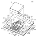
- the semiconductor light emitting device 10 is a device that emits light, and includes a wiring substrate 20, a semiconductor light emitting element 41, and a cap unit 50, as shown in FIG. 3A.
- the semiconductor light emitting device 10 further includes a submount 45, a temperature detecting element 60, a connector 70, and joining members 26, 42, 55, and 62, as shown in FIG.
- each component of the semiconductor light emitting device 10 will be described.
- the wiring board 20 is a plate-shaped member that serves as a base for the semiconductor light emitting device 10 and is provided with wiring.
- the upper surface 20a of the wiring board 20 is a component mounting surface, and the lower surface facing the upper surface 20a (that is, the surface on the back side of the upper surface 20a) is the heat dissipation surface 20b.
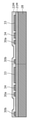
- the wiring board 20 includes a metal substrate 28, a first insulating layer 21, a second insulating layer 22, spacer layers 30a and 30b, a third metal layer 33, and a fourth metal layer. It has 34 and protective films 25 and 35. Further, as shown in FIGS.
- the wiring board 20 further includes a first metal layer 31, a second metal layer 32, a first pad electrode 31p, and a second pad electrode 32p.
- the first metal layer 31, the second metal layer 32, the third metal layer 33, the fourth metal layer 34, and each spacer layer are the second insulating layer. Since it is covered with 22, it does not appear on the surface. However, since the portion of the second insulating layer 22 on each layer projects upward, the position of the edge of each layer is shown as the position of the step of the second insulating layer 22. Further, since each of the above layers is covered with the second insulating layer 22, a broken line leader line is attached to the reference numeral indicating these metal layers. The same applies to each metal layer and each spacer layer shown in the top view and the perspective view described below.
- the wiring board 20 is formed with through holes 28a and 28b and positioning holes 29a and 29b.
- the through holes 28a and 28b are holes for inserting a fixing member such as a screw when fixing the wiring board 20 in close contact with a heat sink or the like.
- the through holes 28a and 28b are arranged on one side and the other side on the opposite side of the region where the semiconductor light emitting element 41 of the wiring board 20 is arranged, respectively.
- the upward direction and the downward direction of FIG. 1B will be referred to as one and the other, respectively.
- the semiconductor light emitting device 41 is arranged between the through hole 28a and the through hole 28b.
- the positioning holes 29a and 29b are holes for positioning with respect to the heat sink or the like when the wiring board 20 is fixed to the heat sink or the like.
- positioning pins provided at positions such as heat sinks where positioning holes 29a and 29b should be arranged are fitted into the positioning holes 29a and 29b, respectively.
- the wiring board 20 can be positioned at a predetermined position such as a heat sink.
- the positioning hole 29a is a first positioning hole, and is a hole having a circular shape in the top view of the wiring board 20.
- the positioning hole 29b is a second positioning hole, and is a hole having an elongated hole shape (that is, an oval shape) in the top view of the wiring board 20.
- the metal substrate 28 is an example of the first substrate of the wiring board 20.
- the metal substrate 28 is composed of a flat plate of a metal such as oxygen-free copper or a copper alloy.
- the flat plate is a plate having a depth or height larger than the surface roughness and having no patterned uneven shape formed on the surface of a surface other than the peripheral portion.
- a flat first insulating layer 21 can be formed on the metal substrate 28. This facilitates the formation of a thick metal layer on the first insulating layer 21.
- the metal substrate 28 is, for example, a flat plate made of oxygen-free copper having a thickness of 0.5 mm or more and 3 mm or less.
- the shape of the metal substrate 28 (that is, the shape in the top view) is, for example, a rectangle, and the length of one side of the metal substrate 28 is, for example, about 5 mm or more and 30 mm or less.
- an oblique cut surface 28c which is an inclined surface inclined with respect to the main surface of the metal substrate 28, is formed on the edge portion of the metal substrate 28.
- the first insulating layer 21 is formed on the upper surface of the metal substrate 28, and the insulating layer is not formed on the lower surface of the metal substrate 28 (that is, the surface on the back side of the upper surface).
- the entire area of the lower surface of the metal substrate 28 can be used as the heat dissipation surface 20b of the wiring board 20, so that heat can be dissipated in a large area. Therefore, it is possible to use a high light output semiconductor light emitting device 41 having a large calorific value.
- the first insulating layer 21 is an insulating layer arranged on the upper surface of the metal substrate 28.
- the first insulating layer 21 is made of an insulating material such as epoxy glass or ceramic having a thickness of 0.05 mm or more and 0.3 mm or less, for example.
- an opening 21a is formed in the first insulating layer 21.
- a part of the first insulating layer 21 is removed to form a rectangular opening 21a.
- the opening 21a is formed at a position closer to the edge than the central portion in the top view of the metal substrate 28.
- a protective film 25 made of Ni, Au, etc. is formed in the region of the metal substrate 28 corresponding to the opening 21a, and a mounting surface for mounting the semiconductor light emitting element 41 is formed. ..
- the semiconductor light emitting element 41 is arranged in the opening 21a via the submount 45.
- the first metal layer 31, the second metal layer 32, the third metal layer 33, and the fourth metal layer 34 are metal layers arranged apart from each other on the first substrate, and in the present embodiment, the first metal layer 31 and the fourth metal layer 34 are arranged apart from each other. 1 Arranged on the insulating layer 21.
- the first metal layer 31 and the second metal layer 32 are wirings for supplying power to the semiconductor light emitting device 41.
- the third metal layer 33 and the fourth metal layer 34 are wirings connected to the temperature detecting element 60.
- Each metal layer forms a convex portion on the first insulating layer 21.
- the first metal layer 31, the second metal layer 32, the third metal layer 33, and the fourth metal layer 34 are, for example, metal layers composed of copper having a thickness of 0.02 mm or more and 0.15 mm or less. ..
- the spacer layers 30a and 30b are layers arranged at positions different from those of the first metal layer 31 and the second metal layer 32 on the first substrate, and are arranged on the first insulating layer 21 in the present embodiment. .. As shown in FIG. 4, the spacer layers 30a and 30b are arranged between the joint surface 50b of the cap unit 50 with the wiring board 20 and the first insulating layer 21. The spacer layers 30a and 30b form convex portions on the first insulating layer 21 in the same manner as the metal layers.
- the materials constituting the spacer layers 30a and 30b are not particularly limited. In this embodiment, the spacer layers 30a and 30b are made of a metal material.
- the spacer layers 30a and 30b are, for example, metal layers made of copper having a thickness of 0.02 mm or more and 0.15 mm or less, similar to the first metal layer 31 and the like.
- the second insulating layer 22 is an insulating layer arranged on the first insulating layer 21.
- the second insulating layer 22 has a function of covering at least a part of the first metal layer 31, the second metal layer 32, the third metal layer 33, the fourth metal layer 34, the spacer layers 30a and 30b, and protecting each of these layers. Also has.
- the second insulating layer 22 is, for example, an insulating layer made of a resin such as polyimide or epoxy having a thickness of 0.05 mm or more and 0.2 mm or less.
- the protective film 25 is a metal film arranged at a position or the like where the submount 45 or the like is joined on the wiring board 20.
- the protective film 25 is arranged in the region corresponding to the opening 21a of the first insulating layer 21 of the metal substrate 28.
- the protective film 35 is a metal film in which a metal layer such as the first metal layer 31 is arranged on a surface exposed from the second insulating layer 22.
- the protective film 35 is arranged on a part of the upper surface of the first metal layer 31, the second metal layer 32, the third metal layer 33, and the fourth metal layer 34.
- the protective films 25 and 35 also have a role of a rust preventive film that protects exposed surfaces such as the metal substrate 28 and the first metal layer 31 from oxidation and the like.
- the protective films 25 and 35 are made of, for example, Ni, Au and the like.
- the first pad electrode 31p and the second pad electrode 32p are pad-shaped electrodes arranged on the portions of the first metal layer 31 and the second metal layer 32 adjacent to the semiconductor light emitting device 41, respectively. As shown in FIGS. 2 and 3A, the metal wires W2 and W3 are bonded to the first pad electrode 31p and the second pad electrode 32p, respectively.
- the first pad electrode 31p and the second pad electrode 32p are also a part of the protective film 35, and are composed of, for example, Ni, Au, and the like.
- the semiconductor light emitting element 41 is a light emitting element arranged on the upper surface 20a of the wiring board 20.
- the semiconductor light emitting device 41 is arranged in the opening 21a of the first insulating layer 21.
- the semiconductor light emitting device 41 is, for example, a light emitting device made of a compound semiconductor such as gallium nitride based or gallium arsenide based.
- the semiconductor light emitting device 41 is a semiconductor laser device having an optical waveguide extending in a direction parallel to the main surface of the metal substrate 28.
- the semiconductor light emitting device 41 is mounted on the submount 45.
- the semiconductor light emitting device 41 has a substrate and a semiconductor laminate laminated on the substrate.
- An optical waveguide is formed on the semiconductor laminate.
- the semiconductor laminate of the semiconductor light emitting device 41 is arranged so as to face the submount 45. That is, the semiconductor light emitting device 41 is junction-down mounted on the submount 45. Electrodes (not shown) are provided on the upper surface (that is, the upper surface of the semiconductor light emitting device 41 in FIG. 4) and the lower surface (that is, the lower surface of the semiconductor light emitting device 41 in FIG. 4) of the semiconductor light emitting device 41, respectively. It is formed.
- the lower surface of the semiconductor light emitting device 41 faces the upper surface of the submount 45.
- the electrode formed on the lower surface of the semiconductor light emitting device 41 facing the submount 45 is electrically connected to the first electrode 47 formed on the upper surface of the submount 45. More specifically, the electrode formed on the lower surface of the semiconductor light emitting device 41 is electrically connected to the first electrode 47 formed on the upper surface of the submount 45 via a joining member 42 (see FIG. 4) made of AuSn solder or the like. Be connected.
- the electrode formed on the upper surface of the semiconductor light emitting device 41 is electrically connected to the second electrode 48 formed on the upper surface of the submount 45 via the metal wire W1.
- the first electrode 47 and the second electrode 48 formed on the upper surface of the submount 45 are electrically connected to the first pad electrode 31p and the second pad electrode 32p, respectively, via the metal wires W2 and W3.
- the current can be supplied to the semiconductor light emitting device 41 by using the first metal layer 31 and the second metal layer 32 connected to the first pad electrode 31p and the second pad electrode 32p, respectively.
- the semiconductor light emitting device 41 has a light emitting point 41e that emits the emitted light L1.
- the emitted light L1 is a laser beam.
- the emitted light L1 is laser light having a peak wavelength in the range of, for example, a wavelength of 270 nm or more and 600 nm or less when the semiconductor light emitting device 41 contains a gallium nitride compound semiconductor, and the semiconductor light emitting device 41 is a gallium phosphate indium type.
- a compound semiconductor or a gallium arsenide compound semiconductor is included, it is, for example, a laser beam having a peak wavelength in the range of 600 nm or more and 10.4 ⁇ m or less.
- the light emitting point 41e is an end portion of the optical waveguide of the semiconductor light emitting device 41 located on the left side of FIG.
- the semiconductor light emitting device 41 is arranged so that the emission surface, which is the end surface on which the light emitting point 41e is arranged, protrudes from the end surface of the submount 45 (the left end surface of the submount 45 shown in FIG. 4). As a result, it is possible to prevent the emitted light L1 emitted from the light emitting point 41e from being blocked by the submount 45.
- the semiconductor light emitting device 41 has, for example, a rectangular parallelepiped shape having a width of 0.2 mm or more and 2 mm or less, a length of 1 mm or more and 9 mm or less, and a thickness of 0.08 mm or more and 0.2 mm or less. ..
- the submount 45 is a member arranged between the wiring board 20 and the semiconductor light emitting element 41.
- the submount 45 is mounted on the upper surface 20a of the wiring board 20. More specifically, as shown in FIG. 4, the submount 45 is arranged inside the opening 21a of the first insulating layer 21 and mounted on the metal substrate 28 via the joining member 26 and the protective film 25. ..
- the joining member 26 is made of, for example, AuSn solder or the like.
- a semiconductor light emitting device 41 is mounted on the upper surface of the submount 45.
- the submount 45 includes an insulating block which is a rectangular parallelepiped block made of an insulating material, a first electrode 47 and a second electrode 48 which are metal films arranged on the upper surface of the insulating block, and the like. It has a metal film (not shown) arranged on the lower surface of the insulating block.
- the insulating block is made of an insulating material having high thermal conductivity such as AlN, SiC, and diamond.
- the insulating block has, for example, a rectangular parallelepiped shape having a width of 1 mm or more and 5 mm or less, a length of 2 mm or more and 10 mm or less, and a thickness of 0.2 mm or more and 4 mm or less.
- the first electrode 47 and the second electrode 48 are arranged apart from each other and are electrically insulated. Further, the first electrode 47 and the second electrode 48 are electrically insulated from the metal film arranged on the lower surface of the insulating block.
- the metal film arranged on the lower surface of the first electrode 47, the second electrode 48, and the insulating block is a metal film made of Ni, Cu, Ti, Pt, Au, or the like.
- the semiconductor light emitting element 41 is mounted on the metal substrate 28 via the submount 45 as described above. With such a configuration, as shown by the arrow in FIG. 4, the heat generated by the semiconductor light emitting device 41 can be efficiently dissipated to the metal substrate 28 via the submount 45.
- the lower surface of the metal substrate 28 is in close contact with, for example, a heat sink (not shown).
- the heat generated by the semiconductor light emitting device 41 can be efficiently conducted from the metal substrate 28 to the heat sink.
- the metal substrate 28 according to the present embodiment is a flat plate, it is easy to manufacture and the cost can be reduced. Therefore, it is possible to realize the semiconductor light emitting device 10 which has a simplified configuration and can be manufactured at low cost.
- the cap unit 50 is a cover member arranged on the upper surface 20a of the wiring board 20 and covering the semiconductor light emitting element 41. As shown in FIG. 4, the cap unit 50 has a joint surface 50b facing the wiring board 20.
- the joining surface 50b has an annular shape, and the joining surface 50b and the upper surface 20a of the wiring board 20 are joined by a joining member 55 made of an epoxy adhesive, a silicon adhesive, AuSn solder, or the like. As a result, the space between the cap unit 50 and the wiring board 20 can be sealed.
- a joining member 55 made of an epoxy adhesive, a silicon adhesive, AuSn solder, or the like.
- the cap unit 50 includes an opening 21a of the first insulating layer 21, a semiconductor light emitting element 41 and a submount 45 arranged in the opening 21a, and a first pad. It covers the electrode 31p and the second pad electrode 32p, and a part of each of the first metal layer 31 and the second metal layer 32.
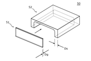
- the cap unit 50 has a rectangular top plate 52d (see FIG. 4) and four side walls 51, 52a, 52b, and 52c (see FIG. 2) connected to the four sides of the peripheral edge of the top plate 52d, respectively. Have.
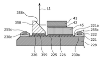
- one of the four side walls 51, 52a, 52b, and 52c is a translucent window, and as shown in FIG. 4, the inorganic translucent plate 51a and the inorganic translucent translucent plate 51a.
- the side wall 51 has antireflection films 51b and 51c arranged on the plate 51a.
- the side wall 51 has antireflection films 51b and 51c arranged on each main surface of the inorganic translucent plate 51a.
- the antireflection film 51b is arranged on the main surface of the inorganic light transmitting plate 51a facing the semiconductor light emitting device 41, and the antireflection film 51c is arranged on the main surface on the back side of the main surface.
- the three side walls 52a, 52b, and 52c and the top plate 52d are integrally formed to form the holder 52.
- the side wall 51 is arranged at a position facing the light emitting point 41e of the semiconductor light emitting element 41. As a result, the light L1 emitted from the semiconductor light emitting device 41 passes through the side wall 51 which is a translucent window.
- the holder 52 is made of glass, for example.
- the holder 52 is manufactured, for example, by forming a recess in a rectangular parallelepiped glass block with a sandblaster or the like and dividing the holder 52.
- the side wall 51 and the holder 52 which are translucent windows, are joined by optical contact or laser welding to form a box-shaped cap unit.
- the cap unit 50 has the above configuration, the emitted light L1 from the semiconductor light emitting element can be easily taken out from the side wall 51 of the cap unit 50.
- the thickness Dg of the side wall 51 which is the translucent window shown in FIG. 4, is about 0.01 mm or more and 0.2 mm or less. Further, the distance Dgap between the side wall 51 which is a translucent window and the exit surface of the semiconductor light emitting element 41 (that is, the end surface including the light emitting point 41e) is larger than zero and less than the thickness Dg of the side wall 51. As a result, the distance (Dg + Dgap) from the light emitting point 41e of the semiconductor light emitting element 41 to the outside of the cap unit 50 can be reduced. Therefore, it is possible to reduce the beam cross-sectional area SL1 of the emitted light L1 on the outer surface of the cap unit 50.
- the size of the optical element can be reduced by reducing the beam cross-sectional area SL1 of the emitted light L1 , and the optical element can be reduced.
- the emitted light L1 can be easily coupled to the lens.
- the thickness of the side walls 52a, 52b, and 52c is larger than the thickness of the side wall 51, which is a translucent window. This makes it possible to increase the structural strength of the holder and the cap unit 50 while reducing the distance (Dg + Dgap) from the light emitting point 41e of the semiconductor light emitting element 41 to the outside of the cap unit 50.
- the semiconductor light emitting device 10 may include a functional element other than the semiconductor light emitting element 41.
- the semiconductor light emitting device 10 includes a temperature detecting element 60 as an example of a functional element.
- the temperature detection element 60 which is an example of the functional element, will be described.
- the temperature detecting element 60 is a temperature sensor arranged on the wiring board 20. As shown in FIG. 4, the temperature detecting element 60 is electrically connected to the third metal layer 33 and the fourth metal layer 34 via the joining member 62 and the protective film 35.
- the protective film 35 is also a pad electrode arranged on the third metal layer 33 and the fourth metal layer 34.
- the temperature detection element 60 is mounted on the surface of the wiring board 20 by a joining member 62 such as SnAgCu cream solder.
- the temperature of the wiring board 20 can be detected by the temperature detecting element 60.
- the temperature of the semiconductor light emitting element 41 mounted on the wiring board 20 via the submount 45 can be estimated. Therefore, the temperature of the semiconductor light emitting element 41 can be estimated by the temperature detecting element 60 and used for controlling the semiconductor light emitting element 41. For example, when the temperature detecting element 60 detects that the temperature of the semiconductor light emitting element 41 is higher than a predetermined threshold value, the current supplied to the semiconductor light emitting element 41 can be reduced or stopped.
- a thermistor can be used as the temperature detecting element 60.
- a predetermined voltage is applied to the temperature detecting element 60, and the current flowing through the temperature detecting element 60 is detected to detect the resistance value of the temperature detecting element 60.
- the temperature of the wiring board 20 can be detected from the correlation between the resistance value and the temperature.
- a voltage is applied to the temperature detecting element 60 via the third metal layer 33 and the fourth metal layer 34.
- the temperature detecting element 60 is arranged outside the cap unit 50. As a result, the cap unit 50 can be miniaturized. Therefore, the space between the cap unit 50 and the wiring board 20 can be easily sealed.
- the connector 70 is a connecting component having terminals connected to each of the first metal layer 31 and the second metal layer 32.
- the connector 70 connects the wiring board 20 and an external electric circuit (not shown).
- the connector 70 is a receptacle further having terminals connected to each of the third metal layer 33 and the fourth metal layer 34, as shown in FIG. 3B and the like.
- a protective film 35 is formed at the ends of the first metal layer 31, the second metal layer 32, the third metal layer 33, and the fourth metal layer 34 on the side farther from the place where the semiconductor light emitting element 41 is arranged.
- the pad electrodes 31q, 32q, 33q, and 34q are formed and connected to the connector 70.
- the connector 70 is mounted on the surface of the wiring board 20 by a joining member (not shown) such as SnAgCu cream solder, and is connected to the pad electrodes 31q, 32q, 33q, and 34q.
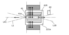
- FIG. 5 is a schematic top view showing the positional relationship between the semiconductor light emitting element 41, each metal layer, and each spacer layer of the semiconductor light emitting device 10 according to the present embodiment and the joint surface 50b of the cap unit 50. ..
- FIG. 5 shows the configuration of the semiconductor light emitting device 41 of the semiconductor light emitting device 10 in a state where the cap unit 50 and the second insulating layer 22 are removed, and the periphery thereof. Further, in FIG. 5, the position of the end edge of the joint surface 50b of the cap unit 50 is shown by a broken line.
- FIG. 6A and 6B are schematic cross-sectional views showing a bonding state between each wiring board according to a comparative example and the present embodiment and a cap unit 50, respectively.
- FIG. 6B shows a wiring board 20 and the like in the cross section of the VI-VI line of FIG.
- FIG. 6A shows a cross section of the wiring board and the cap unit 50 of the comparative example at the same positions as in FIG. 6B.
- 6A and 6B are cross-sectional views (a) before joining the cap unit 50 and each wiring board, and each cross-sectional view (b) shows a cross-sectional view after joining.
- the first pad electrode 31p, the second pad electrode 32p, the first metal layer 31, and the second metal layer 32 extend in the optical axis direction of the semiconductor light emitting device 41 (that is, the optical waveguide extends. It extends in the direction, in other words, in the resonance direction).
- the first pad electrode 31p and the first metal layer 31 are arranged on one side of the semiconductor light emitting device 41 (and the opening 21a).
- the second pad electrode 32p and the second metal layer 32 are arranged on the side of the other side (direction opposite to one side) of the semiconductor light emitting element 41.
- the first metal layer 31 and the second metal layer 32 extend from the inside of the cap unit 50 toward the rear of the semiconductor light emitting device 41 (that is, in the direction opposite to the propagation direction of the emitted light L1) to the outside of the cap unit 50. Stretch. Therefore, the joint surface 50b joined to the wiring board 20 of the cap unit 50 intersects the first metal layer 31 and the second metal layer 32 in the top view of the wiring board 20.
- the portion of the first metal layer 31 where the first pad electrode 31p and the pad electrode 31q are not provided is covered with the second insulating layer 22.
- the portion of the second metal layer 32 to which the second pad electrode 32p and the pad electrode 32q are not provided is covered with the second insulating layer 22.
- the spacer layers 30a and 30b are arranged between the joint surface 50b and the first insulating layer 21.
- the spacer layer 30a is lateral to the other side of the first metal layer 31 (the side closer to the second metal layer 32) on the side of the rear end surface 41R opposite to the emission surface 41F including the light emitting point 41e of the semiconductor light emitting element 41. Therefore, it is arranged so as to extend to one side of the second metal layer 32 (the side closer to the first metal layer 31).
- the spacer layer 30b is composed of five parts.
- the first portion of the spacer layer 30b is laterally (on the main surface of the wiring board 20) from the side of one of the first metal layers 31 (the side far from the second metal layer 32) on the side of the rear end surface 41R. In the plane, it is arranged so as to extend in the direction perpendicular to the optical axis direction).
- the second portion of the spacer layer 30b is connected to the first portion, and the optical axis is on the side of one of the first pad electrode 31p and the first metal layer 31 (the side far from the second metal layer 32). Arranged to extend in the direction.
- the third portion of the spacer layer 30b is connected to the second portion and is arranged so as to extend laterally on the side of the exit surface 41F.
- the fourth portion of the spacer layer 30b is connected to the third portion, and the optical axis is on the side of the second pad electrode 32p and the other side of the second metal layer 32 (the side far from the first metal layer 31). Arranged to extend in the direction.
- the fifth portion of the spacer layer 30b is connected to the fourth portion, and on the side of the rear end surface 41R, from the side of the other side of the second metal layer 32 (the side far from the first metal layer 31). Arranged so as to extend laterally.
- the wiring board of the comparative example shown in FIG. 6A is a wiring board in which the spacer layers 30a and 30b are removed from the wiring board 20 according to the present embodiment.
- the first metal layer 31 and the second metal layer 32 according to the comparative example and the present embodiment have a large cross-sectional area so that a large current can be supplied to the semiconductor light emitting device 41. Therefore, the thickness of the first metal layer 31 and the second metal layer 32 is about 0.02 mm or more and 0.15 mm or less.
- the second insulating layer 22 on each such metal layer is formed by applying a liquid insulating material on the first metal layer 31 and the second metal layer 32 and curing the second metal layer 32, and the thickness is 0. It is about 02 mm or more and 0.1 mm or less.
- the shape of the upper surface of the second insulating layer 22 is an uneven shape along the upper surface of the first insulating layer 21 and each metal layer, as shown in the cross-sectional view (a) of FIG. 6A. That is, on the upper surface of the wiring board, a recess having a depth similar to the thickness of the first metal layer 31 and the second metal layer 32 is formed in the region between the first metal layer 31 and the second metal layer 32. Will be done.
- the joining member layer is crushed, the unnecessary joining member may protrude from the joint surface between the wiring board and the cap unit and spread on the wiring board toward the opening 21a and the connector 70. Therefore, the functions of the functional parts arranged inside and outside the cap unit are changed.
- the hole shape may change.
- the bonding member spreads from the bonding surface facing the light emitting point 41e toward the semiconductor light emitting device 41 the characteristics of the emitted light L1 may change significantly. In order to reduce the influence of the protruding joint member, it is difficult to reduce the size of the semiconductor light emitting device when the distance between the joint surface and the functional component is widened.
- the wiring board 20 and the cap unit 50 are to be bonded with a small amount of joining members, as shown in the cross-sectional view (b) of FIG. 6A, the upper surface of the wiring board and the joining surface 50b of the cap unit 50 A gap 55v in which the joining member 55 does not exist is formed between the two. Therefore, when the wiring board of the comparative example is used, it is not possible to seal between the upper surface of the wiring board and the joint surface 50b of the cap unit 50.
- the first metal layer 31 and the first metal layer 31 are between the joint surface 50b and the first insulating layer 21.
- the spacer layers 30a and 30b are arranged at positions different from those of the second metal layer 32. Since such spacer layers 30a and 30b are arranged between the first metal layer 31 and the second metal layer 32, the first metal layer 31 and the second metal layer 32 on the upper surface 20a of the wiring board 20 The dimensions and depth of the recesses formed between them in the direction parallel to the main surface of the metal substrate 28 can be reduced. Therefore, as shown in the cross-sectional view (b) of FIG.
- the recess of the upper surface 20a of the wiring board 20 can be filled with a small amount of the joining member 55. Therefore, the upper surface 20a of the wiring board 20 and the joining surface 50b of the cap unit 50 can be sealed with a small amount of joining members. Therefore, it is possible to prevent foreign matter and the like from entering the cap unit 50 and to prevent the joint member from affecting the functional parts around the joint surface. That is, a highly reliable semiconductor light emitting device 10 can be realized. Further, since the first metal layer 31 and the second metal layer 32 having a large cross-sectional area are used, a large current can be applied to the semiconductor light emitting device 10 to realize high light output.
- the spacer layers 30a and 30b are a portion of the joint surface 50b facing the first metal layer 31 and a portion facing the second metal layer 32. It is placed along the part between. As a result, it is possible to increase the portion where either the metal layer or the spacer layer is arranged between the joint surface 50b and the wiring board 20. Therefore, it is possible to reduce the formation of a gap between the joint surface 50b and the wiring board 20.
- the spacer layer 30a has a linear shape when viewed from above the wiring board 20, and is located between the portion on the first metal layer 31 and the portion on the second metal layer 32 in the joint surface 50b. Arranged along a straight line.
- the spacer layer 30b has a C-shaped shape when viewed from above the wiring board 20, and is C between the portion on the first metal layer 31 and the portion on the second metal layer 32 in the joint surface 50b. It is arranged along the character-shaped part. As a result, most of the space between the joint surface 50b and the metal substrate 28 where the first metal layer 31 and the second metal layer 32 are not arranged can be filled with the spacer layers 30a and 30b. Therefore, it is possible to further reduce the formation of a gap between the joint surface 50b and the wiring board 20.
- the thicknesses of the spacer layers 30a and 30b are equal to the thicknesses of the first metal layer 31 and the second metal layer 32. Further, the first metal layer 31, the second metal layer 32, the spacer layers 30a and 30b are covered with the second insulating layer 22 having the same thickness. As a result, the upper surface 20a of the wiring board 20 can be made even flatter, so that the formation of a gap between the joint surface 50b and the wiring board 20 can be further reduced. Further, by covering each metal layer and each spacer layer with the second insulating layer 22, it is possible to reduce the disconnection of each metal layer due to the contact of an object from the outside.
- the distance (that is, the gap) between each of the spacer layers 30a and 30b and the first metal layer 31 is the width of the first metal layer 31 (that is, the stretching direction and the thickness direction of the first metal layer 31). It is smaller than the vertical dimension). Further, the distance between each of the spacer layers 30a and 30b and the second metal layer 32 is smaller than the width of the second metal layer 32. As a result, the size of the recess formed on the upper surface 20a of the wiring board 20 can be further reduced. Further, the distance between each of the first metal layer 31 and the second metal layer 32 and the spacer layer 30a may be smaller than the width of the spacer layer 30a.
- the distance between each of the first metal layer 31 and the second metal layer 32 and the spacer layer 30b may be smaller than the width of the spacer layer 30b.
- the size of the recess formed on the upper surface 20a of the wiring board 20 can be further reduced. Therefore, it is possible to further reduce the formation of a gap between the joint surface 50b and the wiring board 20.
- the distance between each of the spacer layers 30a and 30b and the first metal layer 31 may be larger than the thickness of the first metal layer 31.
- the distance between each of the spacer layers 30a and 30b and the second metal layer 32 may be larger than the thickness of the second metal layer 32.
- FIG. 7 is a schematic diagram illustrating each dimension of the first metal layer 31 according to the present embodiment.
- FIG. 8 is a graph showing the relationship between the applied current of the semiconductor light emitting device 10 according to the present embodiment, the operating voltage, and the optical output.
- FIG. 9 is a table showing a design example of the metal layer.
- FIG. 7 shows a schematic diagram of the first metal layer 31 as an example of each metal layer. As shown in FIG. 7, the width of the cross section perpendicular to the stretching direction of the metal layer is W, the thickness is T, and the length in the stretching direction is L. In addition, FIG. 7 also shows the first insulating layer 21 in which the first metal layer 31 is arranged. The dimensions of the metal layers other than the first metal layer 31 are also defined in the same manner as the first metal layer 31.
- the electrical wiring composed of a metal layer has a slight (electrical) resistance.
- a current of 1 ampere or more and 50 amperes or less and a voltage of 2 volts or more and 6 volts or less are applied to the semiconductor light emitting device 41 having a high optical output of 1 watt or more and 100 watts or less.
- the voltage drop in the electrical wiring is 0.2 V even if the wiring resistance is 0.1 ⁇ . That is, the operating voltage increases by 0.2V. Therefore, the wiring resistance cannot be ignored as a factor for increasing the operating voltage of the semiconductor light emitting device 10.
- the Wall-Plug-Efficiency which is the input power-optical conversion efficiency of the semiconductor light emitting device 10
- the Wall-Plug-Efficiency is when the resistance of the electric wiring is high with respect to the value Po / (Va ⁇ If) when the resistance of the electric wiring is low. Decreases with Po / (Vb ⁇ If).
- the effect of this decrease in conversion efficiency on power consumption becomes remarkable.
- a metal layer is formed using a conductive paste containing tungsten as a main component, which is a material suitable for integral sintering. ing.
- tungsten the volume resistivity of tungsten is relatively large, about 5.7 ⁇ 10-8 ⁇ ⁇ m, and tends to be a factor of increasing wiring resistance.
- the metal layer is composed of copper having a volume resistivity of about 1.8 ⁇ 10-8 ⁇ ⁇ m, which is relatively small, or a material containing copper as a main component.
- the metal layer is formed inside the ceramic, it is necessary to improve the adhesion between the metal layer and the ceramic. Therefore, it is necessary to make the thickness T of the metal layer smaller than, for example, 50 ⁇ m. Further, the thickness T of the metal layer may be made smaller than, for example, 20 ⁇ m. As a result, it is possible to reduce the occurrence of irregularities on the surface of the ceramic layer. In such a case, the design conditions of the metal layer for reducing the wiring resistance are limited. For example, when tungsten is used as the material of the metal layer, as shown in FIG. 9, in Design Example 1, since the thickness T and the width W of the metal layer are small, the wiring resistance becomes large. Therefore, the operating voltage increases by 0.228V due to the wiring resistance. Therefore, when the applied current amount is large, it is necessary to increase the thickness T and the width W as in Design Example 2.
- the dimensions of the metal layer are set to the same level as Design Example 2 of the prior art, and the material is changed from tungsten in Design Example 2 to copper.
- the wiring resistance can be reduced to about 1/3 as compared with the design example 2. Therefore, the voltage increase due to the wiring resistance can be reduced to 1% or less of the operating voltage.
- the thickness T of the metal layers constituting the first metal layer 31 and the second metal layer 32 may be 0.05 mm or more. Thereby, the resistance in the first metal layer 31 and the second metal layer 32 can be reduced. Therefore, a convex portion having a height of 0.05 mm or more is formed on the upper surface 20a of the wiring board 20. Further, even when the metal layer and the first insulating layer 21 are covered with a resin such as a resist as the second insulating layer 22, the thickness of the second insulating layer 22 is 0.02 mm or more and 0.1 mm. Since it is about the following, it is difficult to flatten the upper surface 20a of the wiring board 20. Further, the width of each metal layer may be 1 mm or more.
- the wiring resistance of each metal layer can be reduced. Further, in order to reduce the wiring resistance, it is necessary to make the length of each metal layer as short as possible. Therefore, the first metal layer 31 and the second metal layer 32 are connected between the first pad electrode 31p and the second pad electrode 32p and the connector 70 at the shortest distance, for example, in a straight line. Therefore, the distance between the first metal layer 31 and the second metal layer 32 is, for example, 1 mm or more. In this case, even if the cap unit 50 and the wiring board 20 are joined by the joining member 55, the space between the cap unit 50 and the wiring board 20 is, for example, about 0.01 mm or more in the thickness direction and 0. A gap having a space of about 1 mm or more is generated. Therefore, the space between the cap unit 50 and the wiring board 20 cannot be sealed.
- the spacer layers 30a and 30b can narrow the width of the recess formed between each metal layer and each spacer layer to, for example, 0.3 mm or less. As a result, the space between the cap unit 50 and the wiring board 20 can be filled with the joining member 55. Therefore, the space between the cap unit 50 and the wiring board 20 can be sealed.
- the wiring board 20 of the present embodiment has a simplified configuration because it is not necessary to provide wiring in the board.
- each metal layer is used as the material constituting each spacer layer, but the material that can form each spacer layer is not limited to this.
- a resin film such as a polyimide film having the same thickness as each metal layer is formed. , May be used as a spacer layer. As a result, it is possible to prevent each metal layer from being short-circuited with another metal layer via the spacer layer.
- FIGS. 10A to 10G are schematic cross-sectional views illustrating each step of the manufacturing method of the wiring board 20 according to the present embodiment, respectively.
- an oxygen-free copper flat plate having a thickness of 2 mm is prepared.
- an insulating substrate 21M made of a prepreg of epoxy glass is arranged as a material for forming the first insulating layer 21.
- a metal foil 30M made of a copper foil having a thickness of 0.08 mm is arranged on the insulating substrate 21M.
- the metal substrate 28, the insulating substrate 21M, and the metal foil 30M are superposed and heated under pressure to form an integrated substrate as shown in FIG. 10A.
- the metal foil 30M is patterned by etching to form the first metal layer 31, the second metal layer 32, and the spacer layers 30a and 30b.
- the first metal layer 31 and the second metal layer 32 are not shown, but the third metal layer 33 and the fourth metal layer 34 are shown.
- the third metal layer 33 and the fourth metal layer 34 may be formed from the metal foil 30M.
- a resist 22M is formed on the insulating substrate 21M, each metal layer, and each spacer layer.
- the second insulating layer 22 is formed by patterning the resist 22M by a photographic method.
- the second insulating layer 22 is formed with an opening 21a of the first insulating layer 21 and openings 22a to 22d for forming each pad electrode.
- the first insulating layer 21 having the opening 21a is formed by removing the portion of the insulating substrate 21M exposed from the opening 22a by using laser trimming. Form.
- a protective film 25 such as Au is formed on the opening 21a and each metal surface exposed from the openings 22b to 22d by using an electroless plating method.
- the wiring board 20 is formed by separating the metal substrate 28 on which the first insulating layer 21 and the like are formed by using a cutter CT or the like.
- a cutter CT or the like.
- an oblique cut surface 28c having an arbitrary shape can be formed on the wiring board 20.
- the oblique cut surface 28c can be easily formed.
- FIG. 11 is a schematic perspective view illustrating a method of manufacturing the cap unit 50 according to the present embodiment.
- the cap unit 50 is composed of a side wall 51 which is a translucent window and a holder 52.
- the side wall 51 is formed of, for example, a dielectric material such as SiO 2 , Ta 2 O 5 , TiO 2 on both sides of an inorganic translucent plate 51a made of a thin rectangular glass substrate having a thickness Dg of 0.01 mm or more and 0.2 mm or less. It is a translucent window in which antireflection films 51b and 51c made of a multilayer film are formed.
- the holder 52 is a component having a box-like shape lacking one side wall, in which three side walls 52a, 52b, and 52c are connected to three sides of the peripheral edge of a transparent rectangular top plate 52d.
- the holder 52 is manufactured, for example, by forming a recess in a rectangular parallelepiped glass block with a sandblaster or the like and dividing the holder 52.
- the side wall 51 and the holder 52 are joined by optical contact or laser welding to form a box-shaped cap unit 50.
- each side wall of the holder 52 is, for example, 0.3 mm or more and 2 mm or less, which is thicker than the side wall 51. Therefore, even if the side wall 51 thinner than the side walls 52a, 52b, and 52c is used, the side wall 51 is damaged because the side wall 51 is held by the structurally strong holder 52 having the relatively thick side walls 52a, 52b, and 52c. Can be suppressed. Further, by forming the side wall 51 and the holder 52 with the same material, it is possible to prevent damage due to expansion and contraction due to temperature.
- FIG. 12A is a schematic cross-sectional view illustrating a method of attaching the cap unit 50 to the wiring board 20 according to the present embodiment.
- the semiconductor light emitting element 41 and the submount 45 are mounted on the wiring board 20 manufactured by the above-mentioned manufacturing method, and a metal wire (not shown) is attached in advance.
- FIG. 12A shows a cross section perpendicular to the wiring board 20 through the optical axis of the semiconductor light emitting device 41.
- FIG. 12B is a schematic cross-sectional view of a light source device using the semiconductor light emitting device 10 according to the present embodiment.
- the cap unit 50 since the top plate 52d of the cap unit 50 is transparent, as shown in FIG. 12A, the cap is not brought into contact with the side wall 51 which is a translucent window and the emission surface of the semiconductor light emitting element 41.
- the position of the unit 50 can be adjusted with high accuracy. For example, as shown in FIG. 12A, the position of the cap unit 50 is adjusted while observing an enlarged image of the cap unit 50 and the semiconductor light emitting element 41 from above the cap unit 50 using the image observation system 91. You may. This makes it possible to adjust the position of the cap unit 50 so that the distance between the side wall 51 and the exit surface of the semiconductor light emitting element 41 is less than the thickness of the side wall 51.
- the distance between the semiconductor light emitting element 41 and the outside of the cap unit 50 can be reduced.
- the wiring board 20 includes a spacer, and the wiring board 20 and the side wall 51 of the cap unit 50 are joined on the spacer.
- the amount of the bonding member between the wiring board 20 and the side wall 51 can be reduced, so that the excess bonding member reaches the vicinity of the adjacent semiconductor light emitting element 41 and changes the characteristics of the emitted light L1. It can be suppressed.
- a light source device including the semiconductor light emitting device 10 and the lens optical element 92 which is a fast-axis collimating lens.
- the distance DL between the emission surface of the semiconductor light emitting device 41 and the lens optical element 92 can be reduced.
- the beam width of the laser beam (emitted light L1) emitted from the semiconductor light emitting device 10 in the fast axis direction can be reduced.
- the distance obtained by adding the thickness Dg of the side wall 51 and the distance Dgap from the side wall 51 to the exit surface should be short.
- the lens optical element 92 can be brought closer to the emission surface of the semiconductor light emitting element 41 while maintaining the strength of the side wall 51.
- the semiconductor light emitting device 10 of the present embodiment can apply a large current to the semiconductor light emitting element 41 with a small wiring resistance to emit emitted light L1 having a large optical output. Since the semiconductor light emitting element 41 on the wiring board 20 is sealed by the cap unit 50, the reliability of the semiconductor light emitting element 41 can be improved. Further, the distance between the light emitting point 41e of the semiconductor light emitting element 41 and the outside of the cap unit 50 is reduced. Therefore, it is possible to more freely design an external optical element such as a lens optical element that is arranged outside the semiconductor light emitting device 10 and is optically coupled to the light emitting point 41e. Further, as shown in FIG.
- an oblique cut surface 28c is formed at the end portion of the metal substrate 28 of the wiring board on the upper surface 20a side.
- a part of the emitted light L1 can be suppressed from being kicked outside the semiconductor light emitting device, and the external optical element can be arranged more freely.
- the Joule heat generated in the semiconductor light emitting element 41 spreads on the metal substrate 28 and is radiated from the heat radiating surface 20b to the external heat sink. At this time, since the semiconductor light emitting device 41 is mounted on the metal substrate 28 without passing through the first insulating layer 21 and the second insulating layer 22, Joule heat is efficiently transferred to the metal substrate 28.
- the area of the lower surface of the metal substrate 28 is larger than the area of the upper surface due to the diagonally cut surface 28c at the end. Therefore, the Joule heat generated is transferred from the submount 45 to the metal substrate 28 as in the heat flows TP1 and TP5 shown in FIG. 4, and then spreads in a direction parallel to the upper surface of the metal substrate 28, resulting in efficiency. It is well dissipated to the outside. Therefore, the emitted light L1 having a higher light output can be emitted from the semiconductor light emitting element 41.
- the semiconductor light emitting device according to the first modification of the present embodiment will be described.
- the semiconductor light emitting device according to this modification is different from the semiconductor light emitting device 10 according to the first embodiment in the configuration of the spacer layer, and is the same in other configurations.
- the semiconductor light emitting device according to the present modification will be described with reference to FIG. 13A, focusing on the differences from the semiconductor light emitting device 10 according to the first embodiment.
- FIG. 13A is a schematic top view showing the configurations of the spacer layers 130a and 130b of the semiconductor light emitting device 110 according to this modification.
- FIG. 13A shows the configuration of the semiconductor light emitting device 41 of the semiconductor light emitting device 110 in a state where the cap unit 50 and the second insulating layer 22 are removed, and the periphery thereof.
- the spacer layers 130a and 130b according to this modification are made of the same material as the second metal layer 32, and are electrically connected to the second metal layer 32. More specifically, the spacer layers 130a and 130b and the second metal layer 32 have the same thickness, and the upper surfaces of the spacer layers and the second metal layer 32 are connected flat.
- each spacer layer and the second metal layer 32 are connected flush with each other.
- the boundary between the second metal layer 32 and each spacer layer may be appropriately set.
- the second metal layer 32 is defined as a rectangular portion extending in the optical axis direction.
- the spacer layer 130a is an edge of one of the second metal layers 32 (the side closer to the first metal layer 31) on the side of the rear end surface 41R on the side opposite to the emission surface 41F including the light emitting point 41e of the semiconductor light emitting element 41. Therefore, it is arranged so as to extend to the other side of the first metal layer 31 (the side closer to the second metal layer 32).
- the spacer layer 130a is a portion that protrudes from the second metal layer 32 in one direction (in the direction approaching the first metal layer 31).
- the spacer layer 130b is composed of five parts.
- the first portion of the spacer layer 130b is laterally (on the main surface of the wiring board 20) from the side of one of the first metal layers 31 (the side far from the second metal layer 32) on the side of the rear end surface 41R. In the plane, it is arranged so as to extend in the direction perpendicular to the optical axis direction).
- the second portion of the spacer layer 130b is connected to the first portion, and the optical axis is on the side of one of the first pad electrode 31p and the first metal layer 31 (the side far from the second metal layer 32).
- the third portion of the spacer layer 130b is connected to the second portion and is arranged so as to extend laterally on the side of the exit surface 41F.
- the fourth portion of the spacer layer 130b is connected to the third portion, and the optical axis is on the side of the second pad electrode 32p and the other side of the second metal layer 32 (the side far from the first metal layer 31).
- the fifth portion of the spacer layer 130b is connected to the fourth portion, and on the side of the rear end surface 41R, from the other end edge of the second metal layer 32 (the side far from the first metal layer 31). Arranged so as to extend laterally.
- Such spacer layers 130a and 130b can be formed at the same time as the second metal layer 32 in the step of forming each metal layer, similarly to the spacer layers according to the first embodiment. Even when each spacer layer is in contact with the second metal layer 32 as in this modification, each spacer layer is arranged at a position different from that of the second metal layer 32.
- the distance between the second metal layer 32 and each spacer layer is zero. Therefore, among the upper surfaces of the wiring board, the second metal layer 32 and each spacer layer No recess is formed at the corresponding position between and. Therefore, it is possible to reduce the formation of a gap between the joint surface 50b of the cap unit 50 and the upper surface of the wiring board. That is, the joint surface 50b of the cap unit 50 and the upper surface of the wiring board can be more reliably sealed.
- each spacer layer is connected to the second metal layer 32, but each spacer layer may be connected to the first metal layer 31.
- the spacer layers 130a and 130b may be made of the same material as the first metal layer 31. That is, the spacer layers 130a and 130b may be made of the same material as the first metal layer 31 or the second metal layer 32, and may be electrically connected to the first metal layer 31 or the second metal layer 32.
- the semiconductor light emitting device according to the second modification of the present embodiment will be described.
- the semiconductor light emitting device according to this modification is different from the semiconductor light emitting device 10 according to the first embodiment in the configuration of the spacer layer, and is the same in other configurations.
- the semiconductor light emitting device according to the present modification will be described with reference to FIG. 13B, focusing on the differences from the semiconductor light emitting device 10 according to the first embodiment.
- FIG. 13B is a schematic top view showing the configurations of the spacer layers 30a, 30b, and 30c of the semiconductor light emitting device 110a according to this modification.
- FIG. 13B shows the configuration of the semiconductor light emitting device 41 of the semiconductor light emitting device 110a in a state where the cap unit 50 and the second insulating layer 22 are removed, and the periphery thereof.
- the semiconductor light emitting device 110a according to the present modification includes four spacer layers 30c in addition to the spacer layers 30a and 30b similar to those in the first embodiment.
- the spacer layer 30c is an insulating film arranged between each metal layer and the spacer layers 30a and 30b.
- the spacer layer 30c for example, an inorganic material such as a resin or low melting point glass can be used.
- the spacer layers 30a and 30b are made of an insulating material
- the spacer layer 30c may be made of a metal material.
- the gap between each metal layer and the spacer layers 30a and 30b can be filled with the spacer layer 30c. Therefore, from the wiring board 20 according to the first embodiment, the wiring board The size of the recess formed on the upper surface can be reduced. Therefore, it is possible to reduce the formation of a gap between the joint surface 50b of the cap unit 50 and the upper surface of the wiring board. That is, the joint surface 50b of the cap unit 50 and the upper surface of the wiring board can be more reliably sealed.
- the thickness of the spacer layer 30c may be the same as that of each metal layer and the spacer layers 30a and 30b. As a result, the size of the recess formed on the upper surface of the wiring board can be further reduced.
- the semiconductor light emitting device according to the present modification is different from the semiconductor light emitting device 10 according to the first embodiment in that it includes a shielding member arranged between the temperature detecting element 60 and the semiconductor light emitting element 41, and other points. Matches in.
- the semiconductor light emitting device according to the present modification will be described with reference to FIGS. 14A and 14B, focusing on the differences from the semiconductor light emitting device 10 according to the first embodiment.
- 14A and 14B are schematic top views and sectional views showing the positional relationship between the semiconductor light emitting element 41, the temperature detecting element 60, and the shielding member 60s of the semiconductor light emitting device 110b according to this modification, respectively.
- 14B is a cross-sectional view of the semiconductor light emitting device 41 of FIG. 14A on the optical axis LA1.
- the semiconductor light emitting device 110b according to this modification includes a shielding member 60s arranged between the temperature detecting element 60 and the semiconductor light emitting element 41.
- the semiconductor light emitting device 41 also emits the emitted light L1B from the rear end surface 41R, which is the end surface opposite to the emission surface on which the light emitting point 41e is arranged.
- the intensity of the emitted light L1B is significantly smaller than that of the emitted light L1.
- the semiconductor light emitting device 41 is an element having a high light output, the intensity of the emitted light L1B is also relatively high. Therefore, when the emitted light L1B is applied to the temperature detecting element 60, the temperature of the temperature detecting element 60 rises, so that the temperature of the wiring board 20 cannot be accurately detected.
- the shielding member 60s is arranged between the temperature detecting element 60 and the rear end surface 41R of the semiconductor light emitting element 41.
- the semiconductor light emitting element 41, the shielding member 60s, and the temperature detecting element 60 are arranged in this order on the optical axis LA1.
- the shielding member 60s is not particularly limited as long as it can shield the emitted light L1B, but may be, for example, the same element as the temperature detecting element 60. When such an element is used as the shielding member 60s, no wiring is connected to the element.
- the dimension of the shielding member 60s may be larger than that of the temperature detecting element 60. As a result, it is possible to more reliably reduce the incident light L1B on the temperature detecting element 60.
- the shielding member 60s may be arranged outside the cap unit 50 or may be arranged inside.
- the semiconductor light emitting device according to the present embodiment is different from the semiconductor light emitting device 10 according to the first embodiment mainly in the configuration of the first metal layer and the second metal layer.
- the semiconductor light emitting device according to the present embodiment will be described focusing on the differences from the semiconductor light emitting device 10 according to the first embodiment.
- FIGS. 15 to 17 are a schematic perspective view and an exploded perspective view showing the overall configuration of the semiconductor light emitting device 210 according to the present embodiment, respectively.
- FIG. 17 is a schematic cross-sectional view showing the overall configuration of the semiconductor light emitting device 210 according to the present embodiment.
- FIG. 17 is a cross section along the XVII-XVII line of FIG. 16 and shows a cross section perpendicular to the upper surface 220a of the wiring board 220.
- the semiconductor light emitting device 210 includes a wiring board 220, a cap unit 50, and a connector 270. Further, as shown in FIGS. 16 and 17, the semiconductor light emitting device 210 further includes a semiconductor light emitting element 41, a submount 45, and a temperature detecting element 60. Further, as shown in FIG. 17, the semiconductor light emitting device 210 further includes joining members 226, 42, and 62, and a joining layer 255. Hereinafter, each component of the semiconductor light emitting device 210 will be described.
- the wiring board 220 includes a metal substrate 228, a first insulating layer 221, a second insulating layer 222, a third metal layer 233, and a fourth metal layer 234. And a protective film 225.
- the wiring board 20 includes a first metal layer 231 and a second metal layer 232, spacer layers 230a, 230b, and 230c, a first pad electrode 231p, and a second pad electrode. It further has 232p, a first take-out electrode 237, and a second take-out electrode 238.
- the wiring board 220 is formed with through holes 228a and 228b and positioning holes 229a and 229b.
- the through holes 228a and 228b and the positioning holes 229a and 229b according to the present embodiment are different from the through holes 28a and 28b and the positioning holes 29a and 29b according to the first embodiment in the arrangement on the wiring board 220.
- the positioning holes 229a and 229b are arranged near the rear end of the wiring board 220.
- the rear end of the wiring board 220 is the end of the wiring board 220 on the side farther from the light emitting point 41e among the two ends in the propagation direction of the emitted light L1.
- the side on which the emitted light L1 propagates with respect to the semiconductor light emitting device 41 is referred to as a front, and the opposite direction of the front is also referred to as a rear.
- the through holes 228a and 228b are arranged near the center of the wiring board 220 in the propagation direction of the emitted light L1.
- the metal substrate 228 is different from the metal substrate 28 according to the first embodiment in the number and arrangement of the holes provided, and is the same in terms of the points at the ends thereof.
- the first insulating layer 221 is an insulating layer having the same structure as the first insulating layer 21 according to the first embodiment, and an opening 221a is formed.
- the first metal layer 231 and the second metal layer 232, the third metal layer 233, and the fourth metal layer 234 are metal layers arranged apart from each other on the first insulating layer 221.
- the first metal layer 231 extends in a direction perpendicular to the propagation direction of the emitted light L1 from the first pad electrode 231p and parallel to the main surface of the metal substrate 228. , Is connected to the first take-out electrode 237.
- the first metal layer 231 extends from between the first pad electrode 231p and the first insulating layer 221 to between the first extraction electrode 237 and the first insulating layer 221. As shown in FIG.
- the second metal layer 232 extends in a direction perpendicular to the propagation direction of the emitted light L1 from the second pad electrode 232p and parallel to the main surface of the metal substrate 228, and the second extraction electrode 238. Connected to. Specifically, the second metal layer 232 extends from between the second pad electrode 232p and the first insulating layer 221 to between the second extraction electrode 238 and the first insulating layer 221. The second metal layer 232 is stretched in the direction opposite to the stretching direction of the first metal layer 231. As described above, in the present embodiment, the first metal layer 231 and the second metal layer 232 are not connected to the connector 270.
- the first metal layer 231 and the second metal layer 232 have a structure as shown in Design Example 6 of FIG. That is, the first metal layer 231 and the second metal layer 232 are copper films having a thickness T of 0.070 mm, a width W of 7.0 mm, and a length L of 5 mm. As a result, the resistance of the first metal layer 231 and the second metal layer 232 can be set to 0.0002 ⁇ . Therefore, even when a large current of about 30 A is supplied to the semiconductor light emitting device 41, the increase in the operating voltage due to the resistance of each metal layer can be suppressed to about 0.006 V.
- the third metal layer 233 and the fourth metal layer 234 are wirings connected to the temperature detecting element 60, similarly to the third metal layer 33 and the fourth metal layer 34 according to the first embodiment.
- the temperature detecting element 60 is arranged inside the cap unit 50, so that the wiring board 220 of the third metal layer 233 and the fourth metal layer 234 is used.
- the arrangement is different from the third metal layer 33 and the fourth metal layer 34 according to the first embodiment.
- the third metal layer 233 and the fourth metal layer 234 are in the optical axis direction on the side of the rear end surface 41R opposite to the emission surface 41F of the semiconductor light emitting device 41. Arranged to stretch to.
- the joint surface 50b joined to the wiring board 220 of the cap unit 50 intersects the third metal layer 233 and the fourth metal layer 234 in the top view of the wiring board 220.
- the first pad electrode 231p and the second pad electrode 232p have the same configurations as the first pad electrode 31p and the second pad electrode 32p according to the first embodiment, respectively.
- the spacer layers 230a, 230b, and 230c are layers arranged at different positions from the first metal layer 231 and the second metal layer 232 on the first insulating layer 221.
- the spacer layers 230a, 230b, and 230c are arranged between the joint surface 50b of the cap unit 50 with the wiring board 220 and the first insulating layer 221 in the same manner as in each spacer layer according to the first embodiment.
- Each spacer layer forms a convex portion on the first insulating layer 221 in the same manner as each metal layer.
- the spacer layer 230a has an L-shaped shape when viewed from above the wiring board 220, and is composed of two parts.
- the first portion of the spacer layer 230a is light from the rear end surface 41R side of the first metal layer 231 on the side of one of the semiconductor light emitting devices 41 (the side on which the first metal layer 231 of the semiconductor light emitting element 41 is arranged). Arranged so as to extend in the axial direction.
- the second portion of the spacer layer 230a is connected to the first portion and is arranged so as to extend laterally from one side of the third metal layer 233 on the side of the rear end surface 41R.
- the spacer layer 230b has an L-shape when viewed from above the wiring board 220, and is composed of two parts.
- the first portion of the spacer layer 230b is light from the rear end surface 41R side of the second metal layer 232 on the side of the other side of the semiconductor light emitting device 41 (the side where the second metal layer 232 of the semiconductor light emitting element 41 is arranged). Arranged so as to extend in the axial direction.
- the second portion of the spacer layer 230b is connected to the first portion and is arranged laterally extending laterally from the other side of the fourth metal layer 234 on the side of the rear end surface 41R.
- the spacer layer 230c is composed of three parts.
- the first portion of the spacer layer 230c is arranged so as to extend in the optical axis direction from the exit surface 41F side of the first metal layer 231 on one side of the semiconductor light emitting device 41.
- the second portion of the spacer layer 230c is connected to the first portion and is arranged so as to extend laterally on the side of the exit surface 41F.
- the third portion of the spacer layer 230c is connected to the second portion and extends in the optical axis direction from the exit surface 41F side of the second metal layer 232 on the other side of the semiconductor light emitting device 41. Be placed.
- the second insulating layer 222 is an insulating layer arranged on the first insulating layer 221 as shown in FIG.
- the second insulating layer 22 has the same as the second insulating layer 22 according to the first embodiment, that is, the first metal layer 231 and the second metal layer 232, the third metal layer 233, the fourth metal layer 234, and the spacer layer 230a. Covers 230b, and at least a portion of 230c.
- the protective film 225 is a metal film arranged at a position where the submount 45 is joined or the like on the wiring board 220.
- the protective film 225 is arranged in the region corresponding to the opening 221a of the first insulating layer 221 of the metal substrate 228, similarly to the protective film 25 according to the first embodiment.
- the protective film 235 is arranged on a part of the upper surface of the first metal layer 231, the second metal layer 232, the third metal layer 233, the fourth metal layer 234, and the like, similarly to the protective film 35 according to the first embodiment. Will be done.
- the submount 45 is arranged inside the opening 221a of the first insulating layer 221 and is mounted on the metal substrate 228 via the joining member 226 and the protective film 225.
- the joining member 226 is made of, for example, AuSn solder or the like.
- the first take-out electrode 237 and the second take-out electrode 238 are examples of take-out electrodes electrically connected to the first metal layer 231 and the second metal layer 232, respectively.
- the first take-out electrode 237 and the second take-out electrode 238 are arranged on the first metal layer 231 and the second metal layer 232, respectively.
- the first take-out electrode 237 and the second take-out electrode 238 are arranged in the vicinity of the first pad electrode 231p and the second pad electrode 232p, respectively.
- Each of the first take-out electrode 237 and the second take-out electrode 238 has an annular shape, and electrode through holes 237a and 238a penetrating the wiring board 220 are formed in the central portion, respectively.
- the through holes 228a and 228b are holes for inserting a fixing member such as a screw when the wiring board 220 is brought into close contact with the heat sink or the like and fixed.
- the electrode through holes 237a and 238a are arranged on one side and the other side on the opposite side of the region where the semiconductor light emitting element 41 of the wiring board 220 is arranged, respectively. In other words, the semiconductor light emitting device 41 is arranged between the electrode through holes 237a and the electrode through holes 238a.
- the joining layer 255 is a member that joins the joining surface 50b of the cap unit 50 and the upper surface 220a of the wiring board 220.
- the bonding layer 255 has a first bonding preliminary film 255a, a bonding member 255b, and a second bonding preliminary film 255c.
- the first bonding preliminary film 255a and the second bonding preliminary film 255c are metal films arranged on the bonding surface 50b and the upper surface of the second insulating layer 222, respectively, and are composed of Ni, Au, and the like. With these bonding preliminary films, the cap unit 50 and the second insulating layer 222 can be easily bonded by the bonding member 255b.
- the joining member 255b is an alloy member made of AuSn solder or the like.
- the temperature detection element 60 is the same element as the temperature detection element 60 according to the first embodiment.
- the temperature detecting element 60 is covered with the cap unit 50 as shown in FIGS. 16 and 17.
- the temperature detecting element 60 is not exposed to the outside air, and the influence of the outside air on the temperature detection is suppressed, so that the temperature can be detected with high accuracy.
- FIG. 18 is a top view showing the arrangement of the temperature detecting element 60 according to the present embodiment.
- the temperature detecting element 60 is arranged at a position that does not intersect with the optical axis LA1 of the semiconductor light emitting element 41. As a result, it is possible to prevent the temperature detecting element 60 from being irradiated with the emitted light L1B emitted from the rear end surface 41R of the semiconductor light emitting element 41 without arranging the shielding member. Therefore, the temperature of the wiring board 220 can be accurately detected by the temperature detecting element 60.
- the connector 270 is a connecting component having terminals connected to each of the third metal layer 233 and the fourth metal layer 234. In the present embodiment, unlike the connector 70 according to the first embodiment, the connector 270 does not have a terminal connected to the first metal layer 231 and the second metal layer 232.
- FIGS. 19A to 19C are schematic cross-sectional views illustrating a method of joining the cap unit 50 of the semiconductor light emitting device 210 according to the present embodiment to the wiring board 220.
- FIG. 19A shows a cross section similar to that in FIG. 17, but omits parts other than the wiring board 220 and the cap unit 50.
- 19B and 19C show the semiconductor light emitting device 210 in the cross section of the XIX-XIX line of FIG. 16 and perpendicular to the upper surface 220a of the wiring board 220.
- 19A and 19B show a state before joining the cap unit 50 and the wiring board 220
- FIG. 19C shows a state after joining the cap unit 50 and the wiring board 220.
- the first bonding preliminary film 255a and the bonding member 255b are formed on the bonding surface 50b of the cap unit 50 in this order.
- the second bonding preliminary film 255c is formed in the region of the upper surface 220a of the wiring board 220 facing the bonding surface 50b of the cap unit 50.
- the size of the recess formed on the upper surface 220a of the wiring board 220 can be reduced by each spacer layer, as in the first embodiment.
- the cap unit 50 is arranged on the upper surface 220a of the wiring board 220.
- the wiring board 220 is heated to melt the bonding member 255b between the first bonding preliminary film 255a and the second bonding preliminary film 255c.
- the joining member 255b is solidified by cooling the wiring board 220.
- the first bonding preliminary film 255a and the second bonding preliminary film 255c can be bonded by the bonding member 255b.
- the semiconductor light emitting device 210 having high light output and high reliability can be realized as in the first embodiment.
- FIGS. 20 and 21 are a schematic perspective view and an exploded perspective view showing the configuration of the light source device 201 according to the present embodiment, respectively.
- the light source device 201 includes a semiconductor light emitting device 210, a heat sink 219, terminal fixing screws S1 and S2, and fixing screws S3 and S4.
- the light source device 201 further comprises a cable 272 having a connector 271 and cables 211 and 212 having terminals 213 and 214, respectively.
- the heat sink 219 is a heat dissipation component made of a material having high thermal conductivity such as metal.
- the heat sink 219 is composed of, for example, iron, an iron alloy, aluminum, an aluminum alloy, copper, or the like. Further, a surface-treated aluminum alloy having an alumite-treated surface or copper having a Ni-plated surface may be used.
- the heat sink 219 is formed with positioning pins P1 and P2 and screw holes T1 to T4. The positioning pins P1 and P2 are inserted into the positioning holes 229a and 229b of the semiconductor light emitting device 210, respectively.
- the semiconductor light emitting device 210 is fixed in close contact with the heat sink 219 by using the terminal fixing screws S1 and S2 and the fixing screws S3 and S4. Specifically, the fixing screws S3 and S4 penetrate the through holes 228a and 228b of the wiring board, respectively, and are fixed to the screw holes T3 and T4 of the heat sink 219, respectively.
- the terminal fixing screw S1 penetrates the hole formed in the terminal 213 and the electrode through hole 237a of the wiring board 220, and is fixed to the screw hole T1 of the heat sink 219.
- the terminal fixing screw S1 penetrates the electrode through hole 237a, and the terminal 213 is arranged between the terminal fixing screw S1 and the first take-out electrode 237. As a result, the first extraction electrode 237 and the terminal 213 are electrically connected.
- the terminal fixing screw S2 is fixed to the screw hole T2 of the heat sink 219 via the hole formed in the terminal 214 and the electrode through hole 238a of the wiring board 220.
- the terminal fixing screw S2 penetrates the electrode through hole 238a, and the terminal 214 is arranged between the terminal fixing screw S2 and the second take-out electrode 238. As a result, the second extraction electrode 238 and the terminal 214 are electrically connected.
- the semiconductor light emitting device 210 can be fixed to the heat sink 219.
- the semiconductor light emitting device 210 can be firmly fixed to the heat sink 219 by using the terminal fixing screws S1 and S2, and the fixing screws S3 and S4, so that the heat generated by the semiconductor light emitting element 41 of the semiconductor light emitting device 210 can be generated. It can be effectively dissipated from the metal substrate 228 to the heat sink 219.
- the terminals 213 and 214 and the first take-out electrode 237 and the second take-out electrode 238 can be electrically connected, respectively. Therefore, a large current can be supplied to the semiconductor light emitting device 210 via the cables 211 and 212.
- the fixing screws S3 and S4 are made of, for example, a metal material.
- those made of an insulating material such as plastic or ceramic or those having an insulating coating are used in order to suppress a short circuit between each terminal and the metal substrate 228 and the heat sink.
- the connector 271 is connected to the connector 270. As a result, the signal from the temperature detecting element 60 can be acquired via the cable 272.
- FIG. 22A is a schematic cross-sectional view showing a state in which the terminal fixing screw Sc1 according to this modification is fixed to the heat sink 219.
- FIG. 22B is an exploded cross-sectional view showing a method of fixing the terminal fixing screw Sc1 according to the present modification to the heat sink 219.
- the surface of the heat sink 219 is conductive, for example, an aluminum alloy that has not been surface-treated.
- the terminal 213 and the wiring board 220 are fixed to the screw hole T1 of the heat sink 219 by using the terminal fixing screw Sc1 made of a conductive material such as iron or stainless steel.
- a ring-shaped washer Wi that is, a spacer
- an insulating material is inserted between the terminal fixing screw Sc1 and the terminal 213.
- the washer Wi is a washer with a brim with a brim WiC.
- a part of the washer Wi can be arranged inside the through hole of the terminal 213 or inside the electrode through hole 237a of the wiring board.
- the possibility that the terminal fixing screw Sc1 and the first take-out electrode 237 are short-circuited inside the hole can be reduced.
- the terminal 214 and the wiring board 220 can be fixed to the heat sink 219 made of a metal material with a terminal fixing screw made of a metal material.
- the semiconductor light emitting device 210 and the heat sink 219 can be fixed more firmly, and the semiconductor light emitting device 210 and the heat sink 219 can be brought into close contact with each other. Therefore, heat can be dissipated more efficiently from the semiconductor light emitting element 41 of the semiconductor light emitting device 210 to the heat sink 219.
- FIG. 25 shows the semiconductor light emitting device 310 in a part of the cross section in the XXV-XXV line of FIG. 23. Further, FIG. 25 shows a semiconductor light emitting device 310 in a state before the cap unit 350 is joined to the wiring board 220.
- the semiconductor light emitting device 310 includes a wiring board 220, a cap unit 350, and a connector 270. As shown in FIG. 24, the semiconductor light emitting device 310 further includes a semiconductor light emitting element 41, a submount 45, a reflection optical element 358, and a temperature detecting element 60. As shown in FIGS. 23 and 25, the semiconductor light emitting device 310 according to the present embodiment emits the emitted light L1 emitted by the semiconductor light emitting element 41 in a direction perpendicular to the upper surface 220a of the wiring board 220. Specifically, as shown in FIG.
- the semiconductor light emitting device 310 includes a reflecting optical element 358, and the light L1 emitted from the semiconductor light emitting element 41 is reflected by the reflecting optical element 358, and the upper surface of the wiring substrate 220 is formed. It propagates in the direction perpendicular to 220a.
- the reflective surface 358r of the reflective optical element 358 is arranged at a position facing the emission surface of the semiconductor light emitting element 41.
- the reflective surface 358r is inclined by 45 degrees with respect to the optical axis of the semiconductor light emitting device 41.
- the emitted light L1 is reflected by the reflecting surface 358r and propagates in the direction perpendicular to the upper surface 220a of the wiring board 220 and in the direction away from the wiring board 220.
- the reflective optical element 358 is bonded to the protective film 225 of the opening 221a via the bonding preliminary film 359 having the same configuration as the first bonding preliminary film 255a and the bonding member 226. ..
- the cap unit 350 has a transparent rectangular top plate 351 and a holder 352.
- the top plate 351 is a translucent window having the same configuration as the side wall 51 of the cap unit 50 according to the second embodiment. That is, the top plate 351 is a translucent window having an inorganic translucent plate and an antireflection film formed on the inorganic translucent plate. As a result, the light L1 emitted from the semiconductor light emitting device 41 passes through the top plate 351 which is a translucent window.
- the holder 352 is a frame-shaped member having four side walls connected to the four sides of the peripheral edge of the top plate 351.
- the emitted light L1 from the semiconductor light emitting device 41 can be easily taken out from the upper surface of the cap unit 350.
- the cap unit 350 is formed, for example, by joining the top plate 351 to the frame-shaped holder 352 by optical contact or laser welding. Therefore, the top plate 351 and the peripheral portion of the holder 352 are in close contact with each other. Further, a first bonding preliminary film (not shown) is arranged on the surface of the holder 352 facing the top plate 351.
- each spacer layer is arranged between the bonding surface of the wiring board 220 of the cap unit 350 with the upper surface 220a and the first insulating layer 221. Then, the second bonding preliminary film 255c is arranged on each spacer layer. Then, by adhering the holder 352 and the wiring board 220 with an adhesive, the space between the cap unit 350 and the wiring board 220 can be sealed. As a result, the semiconductor light emitting device 310 according to the present embodiment also has the same effect as the semiconductor light emitting device 210 according to the second embodiment.
- the same configuration as in the first embodiment may be adopted.
- the semiconductor light emitting device 310 includes one semiconductor light emitting device 41, but the semiconductor light emitting device 310 may include a plurality of semiconductor light emitting elements 41 (see a figure to be described later). 26).
- the reflective optical element may be arranged at a position facing each emission surface of the plurality of semiconductor light emitting elements 41.
- the plurality of semiconductor light emitting devices 41 may be arranged in an array or in a matrix.
- the reflective optical element having the reflecting surface inclined by 45 degrees with respect to the optical axis is arranged at the position facing the emission surface of the semiconductor light emitting element 41, but other optical elements are arranged. It is also good.
- a reflection optical element in which a wavelength conversion member made of a phosphor layer or the like is arranged on a reflection mirror surface inclined at any angle of 10 degrees or more and 80 degrees or less with respect to the optical axis may be arranged.
- the semiconductor light emitting device 41 for example, a semiconductor laser device using a nitride semiconductor material having a peak wavelength in a wavelength range in which the emitted light L1 is 380 nm or more and 490 nm or less may be used.
- a part of the emitted light L1 emitted from the semiconductor light emitting element 41 is wavelength-converted by the reflecting optical element, so that the light including a part of the emitted light L1 and the wavelength conversion light is converted into the semiconductor light emitting device 310. It can be emitted from the top plate 351 of the above. More specifically, the emitted light L1 may be light having a wavelength in the blue region, and the wavelength conversion light may be light having a wavelength in the yellow region. As a result, it is possible to realize a highly reliable semiconductor light emitting device that emits white light having high brightness and high light output from the top plate 351.
- the reflection optical element a diffraction optical element or a diffusion optical element may be used.
- the light L1 emitted from the semiconductor light emitting element 41 can be emitted from the top plate 351 in an arbitrary direction by the reflecting optical element in a predetermined emission pattern.
- the emitted light L1 having a wavelength in the 900 nm band it is possible to realize a semiconductor light emitting device 310 that emits high-output infrared light and has high reliability.
- Such a semiconductor light emitting device 310 can be used, for example, in a Lidar (light detection and ranking) device or the like.
- the semiconductor light emitting device includes a plurality of semiconductor light emitting elements. Then, the reflective optical element is arranged at a position facing each emission surface of the plurality of semiconductor light emitting elements 41. The plurality of semiconductor light emitting elements 41 and the reflecting optical elements are arranged in a matrix.
- the configuration of the semiconductor light emitting device according to this modification will be described with reference to FIG. 26.
- FIG. 26 is a schematic top view showing the overall configuration of the semiconductor light emitting device 310b according to this modification. Note that FIG. 26 shows a state before the cap unit is attached to the wiring board 320b in order to show the inside of the cap unit. Therefore, the second bonding preliminary film 355c arranged along the bonding surface of the cap unit is shown. In this modification, the plurality of semiconductor light emitting elements 41 and the reflecting optical elements 358 are arranged in a matrix of 3 rows and 3 columns.
- the semiconductor light emitting device 310b includes a wiring substrate 320b, a plurality of semiconductor light emitting elements 41, a plurality of submounts 45, a cap unit (not shown in FIG. 26), a temperature detecting element 60, and a connector. 371 and 372 are provided.
- the wiring board 320b includes a metal substrate (not shown in FIG. 26), a first insulating layer 321, first metal layers 331a to 331c, second metal layers 332a to 332c, a third metal layer 333, and a third metal layer. It has four metal layers 334, spacer layers 530a to 530i, a plurality of first pad electrodes 331p, a plurality of second pad electrodes 332p, and a second insulating layer 322.
- the wiring board 320b is formed with positioning holes 229a and 229b and through holes 228a to 228d.
- the first insulating layer 321 is arranged on a metal substrate, and an opening 321a is formed.
- the first metal layers 331a to 331c are arranged on the first insulating layer 321 and are connected to the first pad electrode 331p and the connector 371.
- the second metal layers 332a to 332c are arranged on the first insulating layer 321 and are connected to the second pad electrode 332p and the connector 372.
- the third metal layer 333 is arranged on the first insulating layer 321 and is connected to the temperature detecting element 60 and the connector 371.
- the fourth metal layer 334 is arranged on the first insulating layer 321 and is connected to the temperature detecting element 60 and the connector 372.
- the second insulating layer 322 is arranged on the first insulating layer 321 and covers at least a part of each first metal layer, each second metal layer, and each spacer layer.
- the spacer layers 530a to 530i are arranged at different positions from the first metal layer and the second metal layer between the joint surface of the cap unit and the top of the first insulating layer 321. Also in this modification, each spacer layer is arranged along the joint surface of the cap unit.
- the semiconductor light emitting element 41 is mounted on the submount 45.
- the three semiconductor light emitting devices arranged in the same row (that is, arranged in the left-right direction in FIG. 26) are electrically connected in series by the metal wire W1.
- the first pad electrode 331p and the second pad electrode 332p are arranged in the lateral direction (horizontal direction in FIG. 26) of the semiconductor light emitting elements 41 arranged in the three row directions. That is, a plurality of semiconductor light emitting elements 41 electrically directly connected are arranged side by side between the first pad electrode 331p and the second pad electrode 332p.
- three semiconductor light emitting elements 41 are arranged in the row direction.
- Three first pad electrodes 331p and three second pad electrodes 332p are arranged in the row direction, and are provided so as to correspond to a plurality of semiconductor light emitting element groups in the three rows.
- Each first pad electrode 331p is connected to the semiconductor light emitting device 41 by a metal wire W2.
- Each second pad electrode 332p is connected to the semiconductor light emitting device 41 by a metal wire W3.
- the plurality of first pad electrodes 331p and the second pad electrodes 332p are provided at opposite positions on the wiring board 320b by the corresponding plurality of first metal layers 331a to 331c and the second metal layers 332a to 332c, respectively. It is connected to the two connectors 371 and 372.
- the light output of the emitted light emitted from the semiconductor light emitting device 310b can be increased as compared with the case where a single semiconductor light emitting element 41 is used. Further, as the light output increases, the heat generated by the semiconductor light emitting device 410 also increases, but according to the semiconductor light emitting device 310b according to this modification, heat can be efficiently exhausted by using a heat sink or the like. Deterioration of the semiconductor light emitting device can be suppressed. Therefore, it is possible to realize a semiconductor light emitting device 310b having high light output and high reliability.
- Such a semiconductor light emitting device 310b can be used as a light source for a projector or the like by using, for example, a semiconductor laser element or the like that emits emitted light having a wavelength in the visible light region such as blue, green, or red as the semiconductor light emitting element 41. Can be used.
- the semiconductor light emitting device according to the present embodiment is different from the semiconductor light emitting device 10 according to the first embodiment in that it includes a plurality of semiconductor light emitting elements.
- the semiconductor light emitting device according to the present embodiment will be described with reference to FIG. 27, focusing on the differences from the semiconductor light emitting device 10 according to the first embodiment.
- FIG. 27 is a schematic top view showing the overall configuration of the semiconductor light emitting device 410 according to the present embodiment. Note that FIG. 27 shows a state before the cap unit is attached to the wiring board 420 in order to show the inside of the cap unit 450. Therefore, the second bonding preliminary film 455c arranged along the bonding surface of the cap unit is shown.
- the semiconductor light emitting device 410 includes a wiring substrate 420, a cap unit 450, semiconductor light emitting elements 441a to 441c, a submount 445, a temperature detecting element 60, a shielding member 60s, and a connector 70. Be prepared.
- the cap unit 450, the temperature detection element 60, and the connector 70 have the same configurations as the cap unit 50, the temperature detection element 60, and the connector 70 according to the first embodiment, respectively.
- the cap unit 450 has a side wall 451 which is a translucent window.
- the shielding member 60s has the same configuration as the shielding member 60s according to the third modification of the first embodiment.
- the temperature detecting element 60 and the shielding member 60s are arranged inside the cap unit 450.
- the wiring board 420 includes a metal substrate 428, a first insulating layer 421, a second insulating layer 422, spacer layers 430a, 430b, 430c, and 430d.
- the spacer layers 430a, 430b, 430c, and 430d, the first metal layer 431, the second metal layer 432, the third metal layer 433, and the fourth metal layer 434 are the second insulating layer 422. Since it is hidden underneath, it is shown by a broken line.
- the wiring board 420 is formed with through holes 428a and 428b and positioning holes 429a and 429b, similarly to the wiring board 20 according to the first embodiment.
- An opening 421a is formed in the first insulating layer as in the first insulating layer 21 according to the first embodiment.
- a protective film made of Ni, Au, or the like is formed in the opening 421a, and a mounting surface for mounting each semiconductor light emitting device is formed.
- the semiconductor light emitting elements 441a to 441c are arranged in the opening via the submount 445.
- the first metal layer 431, the second metal layer 432, the third metal layer 433, and the fourth metal layer 434, the first pad electrode 431p, and the second pad electrode 432p are the first metal according to the first embodiment, respectively. It has the same configuration as the layer 431, the second metal layer 432, the third metal layer 433, the fourth metal layer 434, the first pad electrode 31p, and the second pad electrode 32p.
- the spacer layers 430a, 430b, 430c, and 430d according to the present embodiment have the joint surface of the cap unit 450 with the wiring board 420 and the first wiring board 420, similarly to the spacer layers according to the first embodiment. It is placed between the insulating layer. In the present embodiment, the spacer layer is arranged at a position different from each metal layer on the first insulating layer. As a result, the semiconductor light emitting device 410 according to the present embodiment also has the same effect as the semiconductor light emitting device 10 according to the first embodiment.
- the submount 445 includes an insulating block which is a rectangular parallelepiped block made of an insulating material, first electrodes 447a to 447c which are metal films arranged on the upper surface of the insulating block, and second electrodes 448, and the insulating block. It has a metal film (not shown) arranged on the lower surface.
- the first electrodes 447a to 447c and the second electrode 448 are arranged apart from each other and are electrically insulated. Further, the first electrodes 447a to 447c and the second electrode 448 are electrically insulated from the metal film arranged on the lower surface of the insulating block.
- the metal film arranged on the lower surfaces of the first electrodes 447a to 447c, the second electrode 448, and the insulating block is a metal film made of Ni, Cu, Pi, Au, or the like.
- Each of the semiconductor light emitting devices 441a to 441c has the same configuration as the semiconductor light emitting device 41 according to the first embodiment.
- the semiconductor light emitting devices 441a to 441c are junction-down mounted on the first electrodes 447a to 447c, respectively.
- first pad electrode 431p and the first electrode 447a are connected by a metal wire W2.
- the upper surface of the semiconductor light emitting device 441a and the first electrode 447b are connected by a metal wire W1.
- the upper surface of the semiconductor light emitting device 441b and the first electrode 447c are connected by a metal wire W1.
- the upper surface of the semiconductor light emitting device 441c and the second electrode 448 are connected by a metal wire W1.
- the second electrode 448 and the second pad electrode 432p are connected by a metal wire W3.
- the optical output of the emitted light emitted from the semiconductor light emitting device 410 can be increased as compared with the case where a single semiconductor light emitting element 41 is used. Further, as the light output increases, the heat generated by the semiconductor light emitting device 410 also increases, but according to the semiconductor light emitting device 410 according to the present embodiment, heat can be efficiently exhausted by using a heat sink or the like. Deterioration of each semiconductor light emitting device can be suppressed.
- the semiconductor light emitting device is a semiconductor light emitting device
- the semiconductor light emitting device is not limited to the semiconductor light emitting device.
- the semiconductor light emitting device may be a superluminescent diode or a quantum cascade laser.
- the first substrate may be an insulating substrate.
- the wiring board does not have to have the first insulating layer.
- the temperature detection element is used as an example of the functional element, but other functional elements may be used.
- functional elements for example, light-receiving elements, switching elements such as transistors, various passive elements such as capacitors, inductors, and resistors can also be used.
- the shape of the metal layer or the pad electrode connected to the functional element can be arbitrarily selected according to the type of the functional element and the like.
- the semiconductor light emitting element and the functional element may be electrically connected on the wiring board.
- the semiconductor light emitting device includes the shielding member 60s, but when the temperature detecting element 60 is arranged outside the cap unit 50, the cap unit 50 is a shielding member. May function as. That is, among the four side walls of the cap unit 50, the cap unit 50 functions as a shielding member by reducing the transmittance of light from the semiconductor light emitting element 41 on the side wall facing the rear end surface 41R of the semiconductor light emitting element 41. be able to.
- the semiconductor light emitting device is mounted on the metal substrate via the submount, but may be directly mounted without the submount.
- the semiconductor light emitting device may be mounted on a metal substrate at a junction up.
- FIG. 28 is a schematic perspective view showing the configuration of the semiconductor light emitting device 910 according to the reference example.
- the semiconductor light emitting device 910 includes a wiring board 920, a semiconductor light emitting element 41, a submount 45, a temperature detecting element 60, and a connector 70.
- the semiconductor light emitting device 41, the submount 45, the temperature detecting element 60, and the connector 70 have the same configurations as the semiconductor light emitting element 41, the submount 45, the temperature detecting element 60, and the connector 70 according to the first embodiment.
- the wiring board 920 is different from the wiring board 20 according to the first embodiment in that the configuration of the first insulating layer 921, the configuration of the third metal layer 933 and the fourth metal layer 934, and the spacer layer are not provided. , Other configurations match.
- the opening 921a of the first insulating layer 921 extends to the edge of the wiring board 920. That is, the opening 921a has an opening shape in the first insulating layer 921 that is open on the side surface side in the emission direction of the emission light L1 of the semiconductor light emitting element 41.
- the third metal layer 933 and the fourth metal layer 934 have the same configurations as the third metal layer 233 and the fourth metal layer 234 according to the second embodiment, respectively.
- the second insulating layer 922 has the same configuration as the second insulating layer 222 according to the second embodiment.
- a semiconductor light emitting device having a high light output can also be realized by a semiconductor light emitting device 910 having a configuration that does not have such a cap unit. Further, since the semiconductor light emitting device 910 does not include the cap unit and the spacer layer, the semiconductor light emitting device 910 has a simpler configuration than the semiconductor light emitting device 10 according to the first embodiment, and has a high degree of freedom in design.
- the semiconductor light emitting device and the like of the present disclosure include, for example, a laser processing machine, a vehicle lighting device such as a vehicle headlight, a distance measuring device such as a lighting device and a lidar device, and a light source for a projector as a light source having high light output and high reliability. It can be applied to devices, medical light source devices, inspection light source devices, sterilization light source devices, and the like.
Landscapes
- Physics & Mathematics (AREA)
- Condensed Matter Physics & Semiconductors (AREA)
- General Physics & Mathematics (AREA)
- Electromagnetism (AREA)
- Optics & Photonics (AREA)
- Led Device Packages (AREA)
Abstract
半導体発光装置(10)は、配線基板(20)と、配線基板(20)の上面(20a)に配置される半導体発光素子(41)と、半導体発光素子(41)を覆うキャップユニット(50)とを備え、配線基板(20)は、第1基板と、第1基板上において互いに離間して配置される第1金属層(31)及び第2金属層(32)と、第1基板上に配置されるスペーサ層(30a)及び(30b)とを有し、キャップユニット(50)の配線基板(20)と接合される接合面(50b)は、配線基板(20)の上面視において第1金属層(31)及び第2金属層(32)と交差し、スペーサ層(30a)及び(30b)は、接合面(50b)と、第1基板との間において、第1金属層(31)及び第2金属層(32)と異なる位置に配置される。
Description
本開示は、半導体発光装置、及び光源装置に関する。
半導体レーザ素子などの半導体発光素子を基板上に実装し、キャップで半導体発光素子を覆う半導体発光装置が提案されている(例えば、特許文献1及び2等参照)。
特許文献1及び2には、基板上にサブマウントを介して半導体レーザ素子を実装し、かつ、基板上に半導体レーザ素子をカバーするキャップを配置する構造が提案されている。キャップの側面にはレーザ光を取り出すための透明板が配置されている。
特許文献1及び2では、サブマウント及び基板により半導体レーザ素子の放熱性を高め、かつ、キャップにより半導体レーザ素子を気密封止することで半導体レーザ素子の信頼性を高めようとしている。
特許文献1及び2に記載されたような構造において、キャップの内部に配置される半導体発光素子の高光出力化に伴い、半導体発光素子への大電流の供給が必要となる。このため、半導体発光素子への電流供給用の配線として、大電流の供給に適した断面積の大きい、つまり、抵抗が低い配線を用いる必要がある。このような断面積の大きい配線を基板上に配置する場合、キャップと基板との間に断面積の大きい配線が配置されるため、キャップと基板との間に隙間ができる。このため、キャップと基板との間を密封するのが困難となる。このような問題を回避するために、配線を基板の内部に配置することも可能であるが、基板の構造が複雑になり、コストも増大する。
本開示は、このような課題を解決するものであり、簡素化された構成を有し、かつ、半導体発光素子の高光出力化及び信頼性向上を実現できる半導体発光装置などを提供することを目的とする。
上記課題を解決するために、本開示に係る半導体発光装置の一態様は、配線基板と、前記配線基板の上面に配置される半導体発光素子と、前記配線基板の上面に配置され、前記半導体発光素子を覆うキャップユニットとを備え、前記配線基板は、第1基板と、前記第1基板上において互いに離間して配置される第1金属層及び第2金属層と、前記第1基板に配置されるスペーサ層とを有し、前記キャップユニットの前記配線基板と接合される接合面は、前記配線基板の上面視において前記第1金属層及び前記第2金属層と交差し、前記スペーサ層は、前記接合面と前記第1基板との間において、前記第1金属層及び前記第2金属層と異なる位置に配置される。
また、本開示に係る半導体発光素子の一態様において、前記配線基板は、前記第1基板の上面に配置された第1絶縁層をさらに有し、前記第1金属層、前記第2金属層、及び前記スペーサ層は、前記第1絶縁層上に配置されてもよい。
また、本開示に係る半導体発光素子の一態様において、前記第1基板は、金属基板であってもよい。
また、本開示に係る半導体発光素子の一態様において、前記金属基板が、金属の平面板で構成されてもよい。
また、本開示に係る半導体発光素子の一態様において、前記第1絶縁層に、開口部が形成され、前記半導体発光素子は、前記開口部内に配置されてもよい。
また、本開示に係る半導体発光素子の一態様において、前記スペーサ層は、前記接合面に沿って配置されてもよい。
また、本開示に係る半導体発光素子の一態様において、前記配線基板は、前記第1金属層、前記第2金属層、及び前記スペーサ層の少なくとも一部を覆う第2絶縁層を有してもよい。
また、本開示に係る半導体発光素子の一態様において、前記スペーサ層は、金属材料で構成されてもよい。
また、本開示に係る半導体発光素子の一態様において、前記スペーサ層は、前記第1金属層又は前記第2金属層と同一の材料で構成され、前記第1金属層又は前記第2金属層と電気的に接続されてもよい。
また、本開示に係る半導体発光素子の一態様において、前記キャップユニットは、矩形の天板と、前記天板の周縁の四辺にそれぞれ接続される四つの側壁とを有し、前記四つの側壁のうちの一つは、無機透光板と、前記無機透光板に配置される反射防止膜とを有する透光窓であり、前記半導体発光素子からの出射光は、前記透光窓を透過してもよい。
また、本開示に係る半導体発光素子の一態様において、前記天板は、透明であってもよい。
また、本開示に係る半導体発光素子の一態様において、前記透光窓と前記半導体発光素子の出射面との間隔は、ゼロより大きく、前記透光窓の厚さ未満であってもよい。
また、本開示に係る半導体発光素子の一態様において、前記四つの側壁のうち、前記透光窓以外の側壁の厚さは、前記透光窓の厚さより大きくてもよい。
また、本開示に係る半導体発光素子の一態様において、前記キャップユニットは、矩形の天板と、前記天板の周縁の四辺にそれぞれ接続される四つの側壁とを有し、前記天板は、無機透光板と、前記無機透光板に形成される反射防止膜とを有する透光窓であり、前記半導体発光素子からの出射光は、前記透光窓を透過してもよい。
また、本開示に係る半導体発光素子の一態様において、前記半導体発光装置は、反射光学素子を備え、前記半導体発光素子からの出射光は、前記反射光学素子で反射し、前記配線基板の上面に垂直な方向に伝搬してもよい。
また、本開示に係る半導体発光素子の一態様は、前記配線基板上に配置される機能素子を備えてもよい。
また、本開示に係る半導体発光素子の一態様において、前記機能素子は、前記キャップユニットに覆われてもよい。
また、本開示に係る半導体発光素子の一態様において、前記機能素子は、温度検知素子であってもよい。
また、本開示に係る半導体発光素子の一態様において、前記温度検知素子は、前記半導体発光素子の光軸と交差しない位置に配置されてもよい。
また、本開示に係る半導体発光素子の一態様は、前記温度検知素子と前記半導体発光素子との間に配置される遮蔽部材をさらに備えてもよい。
また、本開示に係る半導体発光素子の一態様において、前記第1基板の端部に斜めカット面を有してもよい。
また、上記課題を解決するために、本開示に係る光源装置の一態様は、前記半導体発光装置と、前記半導体発光装置が配置されるヒートシンクと、前記半導体発光装置を前記ヒートシンクに固定する固定ネジとを備え、前記配線基板には、貫通穴が形成されており、前記固定ネジは、前記貫通穴を貫通して前記ヒートシンクに固定される。
また、本開示に係る光源装置の一態様は、端子を有するケーブルと、端子固定ネジとを備え、前記配線基板は、前記第1金属層と電気的に接続される取り出し電極を有し、前記取り出し電極の中央部に電極貫通穴が形成され、前記端子固定ネジは、前記電極貫通穴を貫通し、前記端子は、前記端子固定ネジと前記取り出し電極との間に配置され、前記取り出し電極と、前記端子が、電気的に接続されてもよい。
本開示によれば、簡素化された構成を有し、かつ、半導体発光素子の高光出力化及び信頼性向上を実現できる半導体発光装置などを提供できる。
以下、本開示の実施の形態について、図面を参照しながら説明する。なお、以下に説明する実施の形態は、いずれも本開示の一具体例を示すものである。したがって、以下の実施の形態で示される、数値、形状、材料、構成要素、及び、構成要素の配置位置や接続形態などは、一例であって本開示を限定する主旨ではない。
また、各図は模式図であり、必ずしも厳密に図示されたものではない。したがって、各図において縮尺等は必ずしも一致していない。なお、各図において、実質的に同一の構成に対しては同一の符号を付しており、重複する説明は省略又は簡略化する。
また、本明細書において、「上方」及び「下方」という用語は、絶対的な空間認識における上方向(鉛直上方)及び下方向(鉛直下方)を指すものではなく、積層構成における積層順を基に相対的な位置関係により規定される用語として用いる。また、「上方」及び「下方」という用語は、2つの構成要素が互いに間隔をあけて配置されて2つの構成要素の間に別の構成要素が存在する場合のみならず、2つの構成要素が互いに接する状態で配置される場合にも適用される。
(実施の形態1)
実施の形態に係る半導体発光装置について説明する。
実施の形態に係る半導体発光装置について説明する。
[1-1.全体構成]
まず、本実施の形態に係る半導体発光装置の全体構成について図1A~図4を用いて説明する。図1A及び図1Bは、それぞれ、本実施の形態に係る半導体発光装置10の全体構成を示す模式的な斜視図及び上面図である。図2は、本実施の形態に係る半導体発光装置10のキャップユニット50の内部の構成を示す模式的な斜視図である。図2においては、キャップユニット50の一部が除去された状態の半導体発光装置10が示されている。図3Aは、本実施の形態に係る半導体発光装置10の全体構成を説明する模式的な分解斜視図である。図3Bは、本実施の形態に係る半導体発光装置10の回路構成を説明する等価回路である。図4は、本実施の形態に係る半導体発光装置10の全体構成を説明する模式的な断面図である。図4には、図1Bに示されるIV-IV線に沿った断面における半導体発光装置10が示されている。
まず、本実施の形態に係る半導体発光装置の全体構成について図1A~図4を用いて説明する。図1A及び図1Bは、それぞれ、本実施の形態に係る半導体発光装置10の全体構成を示す模式的な斜視図及び上面図である。図2は、本実施の形態に係る半導体発光装置10のキャップユニット50の内部の構成を示す模式的な斜視図である。図2においては、キャップユニット50の一部が除去された状態の半導体発光装置10が示されている。図3Aは、本実施の形態に係る半導体発光装置10の全体構成を説明する模式的な分解斜視図である。図3Bは、本実施の形態に係る半導体発光装置10の回路構成を説明する等価回路である。図4は、本実施の形態に係る半導体発光装置10の全体構成を説明する模式的な断面図である。図4には、図1Bに示されるIV-IV線に沿った断面における半導体発光装置10が示されている。
本実施の形態に係る半導体発光装置10は、光を出射する装置であり、図3Aに示されるように、配線基板20と、半導体発光素子41と、キャップユニット50とを備える。本実施の形態では、半導体発光装置10は、図4に示されるように、サブマウント45と、温度検知素子60と、コネクタ70と、接合部材26、42、55及び62とをさらに備える。以下、半導体発光装置10の各構成要素について説明する。
[1-1-1.配線基板]
配線基板20は、半導体発光装置10の基台となり、かつ、配線が設けられた板状部材である。配線基板20の上面20aは、部品実装面であり、上面20aに背向する下面(つまり、上面20aの裏側の面)は、放熱面20bとなる。図4に示されるように、配線基板20は、金属基板28と、第1絶縁層21と、第2絶縁層22と、スペーサ層30a及び30bと、第3金属層33と、第4金属層34と、保護膜25、及び35とを有する。また、配線基板20は、図2及び図3Aに示されるように、第1金属層31と、第2金属層32と、第1パッド電極31pと、第2パッド電極32pとをさらに有する。なお、図1A、図1B、図2、及び図3Aにおいて、第1金属層31、第2金属層32、第3金属層33、第4金属層34、及び各スペーサ層は、第2絶縁層22に覆われているため表面には現れない。しかしながら、第2絶縁層22のうち、上記各層上の部分は、上方に突出するため、上記各層の端縁の位置は、第2絶縁層22の段差の位置として示されている。また、上記各層は、第2絶縁層22によって覆われているため、これらの金属層を示す符号には、破線の引き出し線が付されている。以下で説明する上面図及び斜視図に示される各金属層及び各スペーサ層についても同様である。
配線基板20は、半導体発光装置10の基台となり、かつ、配線が設けられた板状部材である。配線基板20の上面20aは、部品実装面であり、上面20aに背向する下面(つまり、上面20aの裏側の面)は、放熱面20bとなる。図4に示されるように、配線基板20は、金属基板28と、第1絶縁層21と、第2絶縁層22と、スペーサ層30a及び30bと、第3金属層33と、第4金属層34と、保護膜25、及び35とを有する。また、配線基板20は、図2及び図3Aに示されるように、第1金属層31と、第2金属層32と、第1パッド電極31pと、第2パッド電極32pとをさらに有する。なお、図1A、図1B、図2、及び図3Aにおいて、第1金属層31、第2金属層32、第3金属層33、第4金属層34、及び各スペーサ層は、第2絶縁層22に覆われているため表面には現れない。しかしながら、第2絶縁層22のうち、上記各層上の部分は、上方に突出するため、上記各層の端縁の位置は、第2絶縁層22の段差の位置として示されている。また、上記各層は、第2絶縁層22によって覆われているため、これらの金属層を示す符号には、破線の引き出し線が付されている。以下で説明する上面図及び斜視図に示される各金属層及び各スペーサ層についても同様である。
本実施の形態では、配線基板20には、貫通穴28a及び28bと、位置決め穴29a及び29bとが形成されている。貫通穴28a及び28bは、配線基板20をヒートシンクなどに密着させて固定する際に、ネジなど固定部材を挿入するための穴である。貫通穴28a及び28bは、配線基板20の半導体発光素子41が配置される領域に対して一方側とその反対側の他方側とにそれぞれ配置される。なお、以下では、図1Bの上方向、及び下方向を、それぞれ、一方、及び他方と称する。言い換えると、貫通穴28aと貫通穴28bとの間に半導体発光素子41が配置される。
位置決め穴29a及び29bは、配線基板20をヒートシンクなどに固定する際に、ヒートシンクなどに対して位置決めを行うための穴である。例えば、ヒートシンクなどの位置決め穴29a及び29bが配置されるべき位置にそれぞれ設けられた位置決めピンが、位置決め穴29a及び29bに嵌められる。これにより、配線基板20をヒートシンクなどの所定の位置に位置決めできる。本実施の形態では、位置決め穴29aは、第1位置決め穴であり、配線基板20の上面視において、円状の形状を有する穴である。位置決め穴29bは、第2位置決め穴であり、配線基板20の上面視において長穴状(つまり長円状)の形状を有する穴である。
金属基板28は、配線基板20が有する第1基板の一例である。金属基板28は、無酸素銅、銅合金などの金属の平面板で構成される。ここで、平面板とは、周辺部以外の面の表面に、表面粗さより深さ又は高さが大きく、かつ、パターン化された凹凸形状が形成されていない板である。金属基板28の上面を平坦とすることで、金属基板28上に平坦な第1絶縁層21を形成できる。これにより、第1絶縁層21上に厚い金属層を形成しやすくなる。金属基板28は、例えば、厚さ0.5mm以上、3mm以下程度の無酸素銅から構成される平面板である。金属基板28の形状(つまり上面視における形状)は、例えば矩形であり、金属基板28の一辺の長さは、例えば、5mm以上、30mm以下程度である。本実施の形態では、金属基板28の縁部分には、金属基板28の主面に対して傾斜した傾斜面である斜めカット面28cが形成されている。金属基板28の上面には、第1絶縁層21が形成され、金属基板28の下面(つまり上面の裏側の面)には、絶縁層は形成されない。これにより、配線基板20の放熱面20bとして、金属基板28の下面の全面積を利用できるため、大面積において放熱することができる。したがって、発熱量の大きい高光出力の半導体発光素子41を用いることが可能となる。
第1絶縁層21は、図4に示されるように、金属基板28の上面に配置される絶縁層である。第1絶縁層21は、例えば厚さ0.05mm以上、0.3mm以下程度のエポキシガラス、セラミックなどの絶縁材料から構成される。
第1絶縁層21には、図2、図3A、及び図4に示されるように、開口部21aが形成される。本実施の形態では、第1絶縁層21の一部が除去され、矩形状の開口部21aが形成される。開口部21aは、金属基板28の上面視における中央部より端寄りの位置に形成される。金属基板28における開口部21aに対応する領域には、図4に示されるように、Ni、Auなどからなる保護膜25が形成され、半導体発光素子41を搭載するための搭載面が形成される。本実施の形態では、開口部21aには、サブマウント45を介して半導体発光素子41が配置される。
第1金属層31、第2金属層32、第3金属層33、及び第4金属層34は、第1基板上において互いに離間して配置される金属層であり、本実施の形態では、第1絶縁層21上に配置される。第1金属層31及び第2金属層32は、半導体発光素子41に給電するための配線である。第3金属層33及び第4金属層34は、温度検知素子60に接続される配線である。各金属層は、第1絶縁層21上に凸部を形成する。第1金属層31、第2金属層32、第3金属層33、及び第4金属層34は、例えば、厚さ0.02mm以上、0.15mm以下程度の銅から構成される金属層である。
スペーサ層30a及び30bは、第1基板上の第1金属層31及び第2金属層32と異なる位置に配置される層であり、本実施の形態では、第1絶縁層21上に配置される。スペーサ層30a及び30bは、図4に示されるように、キャップユニット50の配線基板20との接合面50bと、第1絶縁層21との間に配置される。スペーサ層30a及び30bは、各金属層と同様に、第1絶縁層21上に凸部を形成する。スペーサ層30a及び30bを構成する材料は特に限定されない。本実施の形態では、スペーサ層30a及び30bは、金属材料で構成される。スペーサ層30a及び30bは、例えば、第1金属層31などと同様の厚さ0.02mm以上、0.15mm以下程度の銅から構成される金属層である。
第2絶縁層22は、第1絶縁層21上に配置される絶縁層である。第2絶縁層22は、第1金属層31、第2金属層32、第3金属層33、第4金属層34、スペーサ層30a及び30bの少なくとも一部を覆い、これらの各層を保護する機能も有する。第2絶縁層22は、例えば、厚さ0.05mm以上、0.2mm以下程度のポリイミド、エポキシなどの樹脂などから構成される絶縁層である。
保護膜25は、配線基板20において、サブマウント45などが接合される位置などに配置される金属膜である。本実施の形態では、保護膜25は、金属基板28の第1絶縁層21の開口部21aに対応する領域に配置される。保護膜35は、第1金属層31などの金属層が第2絶縁層22から露出した面に配置される金属膜である。保護膜35は、第1金属層31、第2金属層32、第3金属層33、及び第4金属層34の上面の一部などに配置される。保護膜25及び35は、金属基板28及び第1金属層31などの露出面などを酸化などから保護する防錆膜の役割も有する。保護膜25及び35は、例えば、Ni、Auなどから構成される。
第1パッド電極31p及び第2パッド電極32pは、それぞれ、第1金属層31及び第2金属層32のうち、半導体発光素子41と隣り合う部分の上に配置されるパッド状の電極である。図2及び図3Aに示されるように、第1パッド電極31p及び第2パッド電極32pには、金属ワイヤW2、W3がそれぞれ接合される。本実施の形態では、第1パッド電極31p及び第2パッド電極32pは、保護膜35の一部でもあり、例えば、Ni、Auなどから構成される。
[1-1-2.半導体発光素子]
半導体発光素子41は、配線基板20の上面20aに配置される発光素子である。半導体発光素子41は、第1絶縁層21の開口部21a内に配置される。半導体発光素子41は、例えば、窒化ガリウム系、砒化ガリウム系などの化合物半導体からなる発光素子である。本実施の形態では、半導体発光素子41は、金属基板28の主面に平行な方向に延伸する光導波路を有する半導体レーザ素子である。
半導体発光素子41は、配線基板20の上面20aに配置される発光素子である。半導体発光素子41は、第1絶縁層21の開口部21a内に配置される。半導体発光素子41は、例えば、窒化ガリウム系、砒化ガリウム系などの化合物半導体からなる発光素子である。本実施の形態では、半導体発光素子41は、金属基板28の主面に平行な方向に延伸する光導波路を有する半導体レーザ素子である。
図4に示されるように、半導体発光素子41は、サブマウント45上に実装される。半導体発光素子41は、基板と基板上に積層される半導体積層体とを有する。半導体積層体に光導波路が形成されている。本実施の形態では、半導体発光素子41の半導体積層体がサブマウント45に対向して配置される。つまり、半導体発光素子41は、サブマウント45にジャンクションダウン実装される。半導体発光素子41の上面(つまり、図4における半導体発光素子41の上側の面)及び下面(つまり、図4における半導体発光素子41の下側の面)には、それぞれ電極(図示せず)が形成されている。半導体発光素子41の下面は、サブマウント45の上面と対向する。図5に示されるように半導体発光素子41のサブマウント45と対向する下面に形成された電極は、サブマウント45の上面に形成された第1電極47と電気的に接続される。より詳しくは、半導体発光素子41の下面に形成された電極は、AuSn半田などからなる接合部材42(図4参照)を介してサブマウント45の上面に形成された第1電極47と電気的に接続される。半導体発光素子41の上面に形成された電極は、金属ワイヤW1を介してサブマウント45の上面に形成された第2電極48と電気的に接続される。サブマウント45の上面に形成された第1電極47及び第2電極48は、それぞれ、第1パッド電極31p及び第2パッド電極32pと金属ワイヤW2及びW3を介して電気的に接続される。このような構成により、第1パッド電極31p及び第2パッド電極32pにそれぞれ接続される第1金属層31及び第2金属層32を用いて半導体発光素子41に電流を供給できる。
図4に示されるように、半導体発光素子41は、出射光L1を出射する発光点41eを有する。本実施の形態では、出射光L1は、レーザ光である。出射光L1は、半導体発光素子41が窒化ガリウム系化合物半導体を含む場合には、例えば波長270nm以上600nm以下の範囲内にピーク波長を有するレーザ光であり、半導体発光素子41が燐化ガリウムインジウム系化合物半導体又は砒化ガリウム系化合物半導体を含む場合には、例えば波長600nm以上10.4μm以下の範囲内にピーク波長を有するレーザ光である。発光点41eは、半導体発光素子41が有する光導波路の図4の左側に位置する端部である。半導体発光素子41は、発光点41eが配置される端面である出射面が、サブマウント45の端面(図4に示されるサブマウント45の左側の端面)から突出するように配置される。これにより、発光点41eから出射した出射光L1がサブマウント45によって遮られることを抑制できる。
半導体発光素子41は、例えば、幅が0.2mm以上、2mm以下程度、長さが1mm以上、9mm以下程度、厚さが0.08mm以上、0.2mm以下程度である直方体状の形状を有する。
[1-1-3.サブマウント]
サブマウント45は、配線基板20と半導体発光素子41との間に配置される部材である。サブマウント45は、配線基板20の上面20aに実装される。より詳しくは、図4に示されるように、サブマウント45は、第1絶縁層21の開口部21aの内部に配置され、接合部材26及び保護膜25を介して、金属基板28に実装される。接合部材26は、例えば、AuSn半田などからなる。サブマウント45の上面には、半導体発光素子41が実装される。本実施の形態では、サブマウント45は、絶縁材料で構成される直方体状のブロックである絶縁ブロックと、絶縁ブロックの上面に配置される金属膜である第1電極47及び第2電極48と、絶縁ブロックの下面に配置される金属膜(図示せず)とを有する。絶縁ブロックは、AlN、SiC、ダイヤモンドなどの熱伝導率が高い絶縁材料で構成される。絶縁ブロックは、例えば、幅が1mm以上、5mm以下程度、長さが2mm以上、10mm以下程度、厚さが0.2mm以上、4mm以下程度である直方体状の形状を有する。第1電極47及び第2電極48は、互いに離間して配置され、電気的に絶縁されている。また、第1電極47及び第2電極48は、絶縁ブロックの下面に配置される金属膜と電気的に絶縁されている。第1電極47、第2電極48及び絶縁ブロックの下面に配置される金属膜は、Ni、Cu、Ti、Pt、Auなどからなる金属膜である。
サブマウント45は、配線基板20と半導体発光素子41との間に配置される部材である。サブマウント45は、配線基板20の上面20aに実装される。より詳しくは、図4に示されるように、サブマウント45は、第1絶縁層21の開口部21aの内部に配置され、接合部材26及び保護膜25を介して、金属基板28に実装される。接合部材26は、例えば、AuSn半田などからなる。サブマウント45の上面には、半導体発光素子41が実装される。本実施の形態では、サブマウント45は、絶縁材料で構成される直方体状のブロックである絶縁ブロックと、絶縁ブロックの上面に配置される金属膜である第1電極47及び第2電極48と、絶縁ブロックの下面に配置される金属膜(図示せず)とを有する。絶縁ブロックは、AlN、SiC、ダイヤモンドなどの熱伝導率が高い絶縁材料で構成される。絶縁ブロックは、例えば、幅が1mm以上、5mm以下程度、長さが2mm以上、10mm以下程度、厚さが0.2mm以上、4mm以下程度である直方体状の形状を有する。第1電極47及び第2電極48は、互いに離間して配置され、電気的に絶縁されている。また、第1電極47及び第2電極48は、絶縁ブロックの下面に配置される金属膜と電気的に絶縁されている。第1電極47、第2電極48及び絶縁ブロックの下面に配置される金属膜は、Ni、Cu、Ti、Pt、Auなどからなる金属膜である。
本実施の形態に係る半導体発光装置10では、以上のように、半導体発光素子41が、サブマウント45を介して金属基板28に実装される。このような構成を備えることにより、図4の矢印で示されるように半導体発光素子41で発生する熱を、サブマウント45を介して、金属基板28へ効率良く放散できる。金属基板28の下面は、例えば、図示しないヒートシンクに密着される。これにより、半導体発光素子41で発生した熱を、金属基板28からヒートシンクへ効率よく伝導させることができる。また、本実施の形態に係る金属基板28は、平面板であるため、製造が容易で、コストも低減できる。したがって、簡素化された構成を有し、低コストで製造可能な半導体発光装置10を実現できる。
[1-1-4.キャップユニット]
キャップユニット50は、図1A、図1B、図2、及び図4に示されるように、配線基板20の上面20aに配置され、半導体発光素子41を覆うカバー部材である。キャップユニット50は、図4に示されるように配線基板20と対向する接合面50bを有する。接合面50bは、環状の形状を有し、接合面50bと配線基板20の上面20aとの間が、エポキシ接着剤、シリコン接着剤、AuSn半田などからなる接合部材55で接合される。これにより、キャップユニット50と配線基板20との間をシールすることができる。本実施の形態では、キャップユニット50は、図2に示されるように、第1絶縁層21の開口部21aと、開口部21aに配置される半導体発光素子41及びサブマウント45と、第1パッド電極31p及び第2パッド電極32pと、第1金属層31及び第2金属層32の各々の一部とを覆う。キャップユニット50は、矩形の天板52d(図4参照)と、天板52dの天板の周縁の四辺にそれぞれ接続される四つの側壁51、52a、52b、及び52c(図2参照)とを有する。本実施の形態では、四つの側壁51、52a、52b、及び52cのうち、一つの側壁51は、透光窓であり、図4に示されるように、無機透光板51aと、無機透光板51aに配置される反射防止膜51b及び51cを有する。本実施の形態では、側壁51は、無機透光板51aの各主面に配置される反射防止膜51b及び51cを有する。反射防止膜51bは、無機透光板51aの半導体発光素子41と対向する主面に配置され、反射防止膜51cは、当該主面の裏側の主面に配置される。三つの側壁52a、52b、及び52cと、天板52dとは一体的に形成されており、ホルダ52を構成する。側壁51は、半導体発光素子41の発光点41eと対向する位置に配置される。これにより、半導体発光素子41からの出射光L1は、透光窓である側壁51を透過する。
キャップユニット50は、図1A、図1B、図2、及び図4に示されるように、配線基板20の上面20aに配置され、半導体発光素子41を覆うカバー部材である。キャップユニット50は、図4に示されるように配線基板20と対向する接合面50bを有する。接合面50bは、環状の形状を有し、接合面50bと配線基板20の上面20aとの間が、エポキシ接着剤、シリコン接着剤、AuSn半田などからなる接合部材55で接合される。これにより、キャップユニット50と配線基板20との間をシールすることができる。本実施の形態では、キャップユニット50は、図2に示されるように、第1絶縁層21の開口部21aと、開口部21aに配置される半導体発光素子41及びサブマウント45と、第1パッド電極31p及び第2パッド電極32pと、第1金属層31及び第2金属層32の各々の一部とを覆う。キャップユニット50は、矩形の天板52d(図4参照)と、天板52dの天板の周縁の四辺にそれぞれ接続される四つの側壁51、52a、52b、及び52c(図2参照)とを有する。本実施の形態では、四つの側壁51、52a、52b、及び52cのうち、一つの側壁51は、透光窓であり、図4に示されるように、無機透光板51aと、無機透光板51aに配置される反射防止膜51b及び51cを有する。本実施の形態では、側壁51は、無機透光板51aの各主面に配置される反射防止膜51b及び51cを有する。反射防止膜51bは、無機透光板51aの半導体発光素子41と対向する主面に配置され、反射防止膜51cは、当該主面の裏側の主面に配置される。三つの側壁52a、52b、及び52cと、天板52dとは一体的に形成されており、ホルダ52を構成する。側壁51は、半導体発光素子41の発光点41eと対向する位置に配置される。これにより、半導体発光素子41からの出射光L1は、透光窓である側壁51を透過する。
ホルダ52は、例えば、ガラスからなる。ホルダ52は、例えば、直方体状のガラスブロックに、サンドブラスタなどによって凹部を形成し分割することによって製造される。
透光窓である側壁51とホルダ52とは、オプティカルコンタクト又はレーザ溶接で接合され、箱型のキャップユニットが形成される。
キャップユニット50が以上の構成を有することにより、半導体発光素子からの出射光L1をキャップユニット50の側壁51から容易に外部に取り出すことができる。
図4に示される透光窓である側壁51の厚さDgは、0.01mm以上、0.2mm以下程度である。また、透光窓である側壁51と半導体発光素子41の出射面(つまり、発光点41eを含む端面)との間隔Dgapは、ゼロより大きく側壁51の厚さDg未満である。これにより、半導体発光素子41の発光点41eからキャップユニット50の外部までの距離(Dg+Dgap)を小さくすることができる。したがって、キャップユニット50の外表面での出射光L1のビーム断面積SL1を低減することができる。例えば、キャップユニット50の外部に配置されるレンズなどの光学素子に出射光L1を入射する場合、出射光L1のビーム断面積SL1を低減することで、光学素子の寸法を低減でき、光学素子に出射光L1を容易に結合させることができる。
側壁52a、52b、及び52cの厚さは、透光窓である側壁51の厚さより大きい。これにより、半導体発光素子41の発光点41eからキャップユニット50の外部までの距離(Dg+Dgap)を低減しつつ、ホルダ及びキャップユニット50の構造的な強度を高めることが可能となる。
[1-1-5.機能素子]
半導体発光装置10は、半導体発光素子41以外の機能素子を備えてもよい。本実施の形態においては、半導体発光装置10は、機能素子の一例として温度検知素子60を備える。以下、機能素子の一例である温度検知素子60について説明する。温度検知素子60は、配線基板20上に配置される温度センサである。図4に示されるように、温度検知素子60は、接合部材62及び保護膜35を介して、第3金属層33及び第4金属層34と電気的に接続される。保護膜35は、第3金属層33及び第4金属層34上に配置されるパッド電極でもある。温度検知素子60は、例えばSnAgCuクリーム半田などである接合部材62により、配線基板20上の表面に実装される。温度検知素子60によって配線基板20の温度を検知できる。配線基板20の温度を検知することで、配線基板20にサブマウント45を介して実装された半導体発光素子41の温度を推測することができる。したがって、温度検知素子60によって半導体発光素子41の温度を推測し、半導体発光素子41の制御に用いることができる。例えば、半導体発光素子41の温度が所定の閾値より高いことを温度検知素子60によって検知した場合に、半導体発光素子41へ供給する電流を低減すること、又は、停止することができる。温度検知素子60として、例えば、サーミスタを用いることができる。この場合、温度検知素子60に所定の電圧を印加し、温度検知素子60に流れる電流を検出することで、温度検知素子60の抵抗値を検出する。この抵抗値と温度との相関から配線基板20の温度を検知できる。温度検知素子60には、第3金属層33及び第4金属層34を介して電圧が印加される。本実施の形態では、温度検知素子60は、キャップユニット50の外部に配置される。これにより、キャップユニット50を小型化することができる。したがって、キャップユニット50と配線基板20との間を容易に密封できる。
半導体発光装置10は、半導体発光素子41以外の機能素子を備えてもよい。本実施の形態においては、半導体発光装置10は、機能素子の一例として温度検知素子60を備える。以下、機能素子の一例である温度検知素子60について説明する。温度検知素子60は、配線基板20上に配置される温度センサである。図4に示されるように、温度検知素子60は、接合部材62及び保護膜35を介して、第3金属層33及び第4金属層34と電気的に接続される。保護膜35は、第3金属層33及び第4金属層34上に配置されるパッド電極でもある。温度検知素子60は、例えばSnAgCuクリーム半田などである接合部材62により、配線基板20上の表面に実装される。温度検知素子60によって配線基板20の温度を検知できる。配線基板20の温度を検知することで、配線基板20にサブマウント45を介して実装された半導体発光素子41の温度を推測することができる。したがって、温度検知素子60によって半導体発光素子41の温度を推測し、半導体発光素子41の制御に用いることができる。例えば、半導体発光素子41の温度が所定の閾値より高いことを温度検知素子60によって検知した場合に、半導体発光素子41へ供給する電流を低減すること、又は、停止することができる。温度検知素子60として、例えば、サーミスタを用いることができる。この場合、温度検知素子60に所定の電圧を印加し、温度検知素子60に流れる電流を検出することで、温度検知素子60の抵抗値を検出する。この抵抗値と温度との相関から配線基板20の温度を検知できる。温度検知素子60には、第3金属層33及び第4金属層34を介して電圧が印加される。本実施の形態では、温度検知素子60は、キャップユニット50の外部に配置される。これにより、キャップユニット50を小型化することができる。したがって、キャップユニット50と配線基板20との間を容易に密封できる。
[1-1-6.コネクタ]
コネクタ70は、第1金属層31及び第2金属層32の各々と接続される端子を有する接続部品である。コネクタ70は、配線基板20と外部電気回路(図示せず)とを接続する。本実施の形態では、コネクタ70は、図3Bなどに示されるように、第3金属層33及び第4金属層34の各々と接続される端子をさらに有するレセプタクルである。第1金属層31、第2金属層32、第3金属層33、及び第4金属層34の、半導体発光素子41が配置される場所より遠い側の端部には、保護膜35で構成されたパッド電極31q、32q、33q、及び34qが形成され、コネクタ70と接続される。コネクタ70はSnAgCuクリーム半田などの接合部材(図示せず)により配線基板20の表面に実装され、パッド電極31q、32q、33q、及び34qと接続される。
コネクタ70は、第1金属層31及び第2金属層32の各々と接続される端子を有する接続部品である。コネクタ70は、配線基板20と外部電気回路(図示せず)とを接続する。本実施の形態では、コネクタ70は、図3Bなどに示されるように、第3金属層33及び第4金属層34の各々と接続される端子をさらに有するレセプタクルである。第1金属層31、第2金属層32、第3金属層33、及び第4金属層34の、半導体発光素子41が配置される場所より遠い側の端部には、保護膜35で構成されたパッド電極31q、32q、33q、及び34qが形成され、コネクタ70と接続される。コネクタ70はSnAgCuクリーム半田などの接合部材(図示せず)により配線基板20の表面に実装され、パッド電極31q、32q、33q、及び34qと接続される。
[1-2.作用及び効果]
次に、本実施の形態に係る半導体発光装置10の作用及び効果について、上述した図4及び図5~図6Bを用いて説明する。図5は、本実施の形態に係る半導体発光装置10の半導体発光素子41、各金属層、及び各スペーサ層と、キャップユニット50の接合面50bとの位置関係を示す模式的な上面図である。図5には、キャップユニット50及び第2絶縁層22が除去された状態の半導体発光装置10の半導体発光素子41及びその周辺の構成が示されている。また、図5にはキャップユニット50の接合面50bの端縁の位置が破線で示されている。図6A及び図6Bは、それぞれ、比較例及び本実施の形態に係る各配線基板と、キャップユニット50との間の接合状態を示す模式的な断面図である。図6Bは、図5のVI-VI線の断面における配線基板20などを示す。図6Aは、比較例の配線基板及びキャップユニット50の図6Bと同様の位置における断面を示す。図6A及び図6Bの各断面図(a)は、キャップユニット50と各配線基板との接合前の断面図を示し、各断面図(b)は、接合後の断面図を示す。
次に、本実施の形態に係る半導体発光装置10の作用及び効果について、上述した図4及び図5~図6Bを用いて説明する。図5は、本実施の形態に係る半導体発光装置10の半導体発光素子41、各金属層、及び各スペーサ層と、キャップユニット50の接合面50bとの位置関係を示す模式的な上面図である。図5には、キャップユニット50及び第2絶縁層22が除去された状態の半導体発光装置10の半導体発光素子41及びその周辺の構成が示されている。また、図5にはキャップユニット50の接合面50bの端縁の位置が破線で示されている。図6A及び図6Bは、それぞれ、比較例及び本実施の形態に係る各配線基板と、キャップユニット50との間の接合状態を示す模式的な断面図である。図6Bは、図5のVI-VI線の断面における配線基板20などを示す。図6Aは、比較例の配線基板及びキャップユニット50の図6Bと同様の位置における断面を示す。図6A及び図6Bの各断面図(a)は、キャップユニット50と各配線基板との接合前の断面図を示し、各断面図(b)は、接合後の断面図を示す。
図5に示されるように、第1パッド電極31p、第2パッド電極32p、第1金属層31、及び第2金属層32は、半導体発光素子41の光軸方向(つまり、光導波路の延伸する方向、さらに言い換えると共振方向)に延伸する。第1パッド電極31pと第1金属層31は、半導体発光素子41(及び開口部21a)の一方の側方に配置される。第2パッド電極32pと第2金属層32は、半導体発光素子41の他方(一方と反対側の方向)の側方に配置される。
第1金属層31及び第2金属層32は、キャップユニット50の内部から半導体発光素子41の後方に向かって(つまり、出射光L1の伝搬の向きと逆向きに)キャップユニット50の外部にまで延伸する。このためキャップユニット50の配線基板20と接合される接合面50bは、配線基板20の上面視において第1金属層31及び第2金属層32と交差する。なお、第1金属層31のうち第1パッド電極31p及びパッド電極31qが設けられていない部分は、第2絶縁層22で覆われる。第2金属層32のうち第2パッド電極32p及びパッド電極32qが設けられていない部分は、第2絶縁層22で覆われる。
また、図4及び図5に示されるように、また、スペーサ層30a及び30bは、接合面50bと、第1絶縁層21との間に配置される。スペーサ層30aは、半導体発光素子41の発光点41eを含む出射面41Fと反対側の後端面41Rの側方において、第1金属層31の他方(第2金属層32から近い側)の側方から、第2金属層32の一方(第1金属層31から近い側)の側方に、延伸するように配置される。スペーサ層30bは、5つの部分からなる。スペーサ層30bの第1の部分は、後端面41Rの側方において、第1金属層31の一方(第2金属層32から遠い側)の側方から、横方向(配線基板20の主面の面内で、光軸方向と垂直な方向)に延伸するように配置される。スペーサ層30bの第2の部分は、第1の部分と接続され、かつ、第1パッド電極31pと第1金属層31の一方(第2金属層32から遠い側)の側方において、光軸方向に延伸するように配置される。スペーサ層30bの第3の部分は、第2の部分と接続され、かつ、出射面41Fの側方において、横方向に延伸するように配置される。スペーサ層30bの第4の部分は、第3の部分と接続されるとともに、第2パッド電極32pと第2金属層32の他方(第1金属層31から遠い側)の側方において、光軸方向に延伸するように配置される。スペーサ層30bの第5の部分は、第4の部分と接続され、かつ、後端面41Rの側方において、第2金属層32の他方(第1金属層31から遠い側)の側方から、横方向に延伸するように配置される。
この構成による効果について、図6A及び図6Bを用いて説明する。図6Aに示される比較例の配線基板は、本実施の形態に係る配線基板20からスペーサ層30a及び30bを除去した配線基板である。
比較例及び本実施の形態に係る第1金属層31及び第2金属層32は、半導体発光素子41に大電流を供給できるように大きい断面積を有する。このため、第1金属層31及び第2金属層32の厚さは0.02mm以上、0.15mm以下程度である。このような各金属層上の第2絶縁層22は、液体状の絶縁材料を第1金属層31及び第2金属層32の上に塗布し硬化させることで形成され、厚さは、0.02mm以上、0.1mm以下程度である。このため、第2絶縁層22の上面の形状は、図6Aの断面図(a)に示されるように、第1絶縁層21及び各金属層の上面に沿った凹凸形状となる。つまり、配線基板の上面において、第1金属層31と第2金属層32との間の領域には、第1金属層31及び第2金属層32の厚さと同程度の深さの凹部が形成される。
図6Aに示されるようなスペーサを配置しない比較例の配線基板を用いる場合、配線基板の上面の凹部とキャップユニット50との間に間隔の大きな間隙が形成される。そこで配線基板とキャップユニットとの間を接合部材で充填させるため、接合部材を配線基板上に所定の厚みで塗布し、キャップユニットで接合部材を押し潰して間隙を充填させる方法が考えられる。この場合、大量の接合部材を用いて配線基板表面の凹凸の高さよりも十分に厚い接合部材層を接合面50bの位置に沿って予め形成する。したがって、接合部材層を押し潰す際、不要な接合部材は、配線基板とキャップユニットとの接合面との間からはみ出して、配線基板上を開口部21a及びコネクタ70に向かって拡がり得る。このため、キャップユニットの内側及び外側に配置されている機能部品の機能を変化させてしまう。特に接合部材が貫通穴28a、28b、及び、位置決め穴29a、29b側へ拡がった場合は穴形状が変化する場合がある。また接合部材が、発光点41eに対向する接合面から半導体発光素子41に向かって拡がった場合は、出射光L1の特性が大幅に変化する可能性がある。はみ出した接合部材の影響を小さくするため、接合面と機能部品との距離を広くする場合は、半導体発光装置の小型化が難しくなる。また、配線基板20とキャップユニット50とを少量の接合部材で接着させようとした場合、図6Aの断面図(b)に示されるように、配線基板の上面とキャップユニット50の接合面50bとの間に、接合部材55が存在しない隙間55vが形成される。したがって、比較例の配線基板を用いる場合には、配線基板の上面とキャップユニット50の接合面50bとの間を密封することができない。
一方、本実施の形態に係る配線基板20では、図6Bの断面図(a)に示されるように、接合面50bと、第1絶縁層21との間であって、第1金属層31及び第2金属層32と異なる位置にスペーサ層30a及び30bが配置される。このようなスペーサ層30a及び30bが第1金属層31と第2金属層32との間などに配置されるため、配線基板20の上面20aの第1金属層31と第2金属層32との間に形成される凹部の金属基板28の主面に平行な方向の寸法及び深さを低減できる。したがって、図6Bの断面図(b)に示されるように、配線基板20の上面20aの凹部を少量の接合部材55で埋めることができる。このため、配線基板20の上面20aと、キャップユニット50の接合面50bとの間を少量の接合部材で密封することができる。よって、キャップユニット50内に異物などが進入することを抑制するとともに、接合部材が接合面周辺の機能部品に影響を及ぼすことを抑制できる。つまり、信頼性の高い半導体発光装置10を実現できる。また、断面積の大きい第1金属層31及び第2金属層32を用いているため、半導体発光装置10に大電流を印加し高光出力化を実現できる。
また、本実施の形態では、図5に示されるように、スペーサ層30a及び30bは、接合面50bのうち、第1金属層31と対向する部分と、第2金属層32と対向する部分との間の部分に沿って配置される。これにより、接合面50bと配線基板20との間に、各金属層、又は、各スペーサ層のいずれかが配置される部分を増大させることができる。したがって、接合面50bと配線基板20との間に隙間が形成されることを低減できる。また、スペーサ層30aは、配線基板20の上面視において直線状の形状を有し、接合面50bのうち、第1金属層31上の部分と、第2金属層32上の部分との間の直線状の部分に沿って配置される。スペーサ層30bは、配線基板20の上面視においてC字状の形状を有し、接合面50bのうち、第1金属層31上の部分と、第2金属層32上の部分との間のC字状の部分に沿って配置される。これにより、接合面50bと金属基板28との間の空間のうち、第1金属層31及び第2金属層32が配置されない部分の多くをスペーサ層30a及び30bによって埋めることができる。したがって、接合面50bと配線基板20との間に隙間が形成されることをより一層低減できる。
本実施の形態では、スペーサ層30a及び30bの厚さは、第1金属層31及び第2金属層32の厚さと等しい。また、第1金属層31、第2金属層32、スペーサ層30a及び30bは、同一の厚さの第2絶縁層22で覆われている。これにより、配線基板20の上面20aをより一層平坦にすることができるため、接合面50bと配線基板20との間に隙間が形成されることをより一層低減できる。また、第2絶縁層22で、各金属層と各スペーサ層とを覆うことにより、外部からの物体の接触により各金属層が断線することを低減できる。
また、スペーサ層30a及び30bの各々と、第1金属層31との間の距離(つまり隙間)は、第1金属層31の幅(つまり、第1金属層31の延伸方向及び厚さ方向に垂直な方向の寸法)よりも小さい。また、スペーサ層30a及び30bの各々と、第2金属層32との間の距離は、第2金属層32の幅よりも小さい。これにより、配線基板20の上面20aに形成される凹部の寸法をより一層低減できる。さらに、第1金属層31及び第2金属層32の各々と、スペーサ層30aとの間の距離を、スペーサ層30aの幅よりも小さくしてもよい。さらに、第1金属層31及び第2金属層32の各々と、スペーサ層30bとの間の距離を、スペーサ層30bの幅よりも小さくしても良い。これにより、配線基板20の上面20aに形成される凹部の寸法をより一層低減できる。したがって、接合面50bと配線基板20との間に隙間が形成されることをより一層低減できる。なお、スペーサ層30a及び30bの各々と、第1金属層31との間の距離は、第1金属層31の厚さより大きくてもよい。また、スペーサ層30a及び30bの各々と、第2金属層32との間の距離は、第2金属層32の厚さより大きくてもよい。これにより、スペーサ層30a及び30bが、金属である場合に、第1金属層31と第2金属層とが短絡することを抑制できる。
続いて、図7~図9を用いて、各金属層の設計例について説明する。図7は、本実施の形態に係る第1金属層31の各寸法を説明する模式図である。図8は、本実施の形態に係る半導体発光装置10の印加電流と、動作電圧及び光出力との関係を示すグラフである。図9は、金属層の設計例を示す表である。
図7には、各金属層の一例として第1金属層31の模式図が示されている。図7に示されるように、金属層の延伸方向に垂直な断面の幅をW、厚さをTとし、延伸方向の長さをLとする。なお、図7には、第1金属層31が配置される第1絶縁層21も併せて示されている。なお、第1金属層31以外の他の金属層の寸法についても、第1金属層31と同様に定義される。
金属層で構成された電気配線は、わずかであるが(電気)抵抗を有する。しかしながら、光出力の大きい半導体発光素子41に電力を供給する場合、供給電流量が大きいため、電気配線のわずかな抵抗も無視できない。光出力が1ワット以上、100ワット以下程度の高光出力の半導体発光素子41には、例えば、1アンペア以上、50アンペア以下程度の電流、及び、2ボルト以上、6ボルト以下程度の電圧が印加される。例えば、印加電流2アンペア、動作電圧2ボルトの半導体発光素子41を用いた場合、配線抵抗が0.1Ωであっても、電気配線における電圧降下が0.2Vとなる。つまり、動作電圧が0.2V上昇する。このため、配線抵抗は、半導体発光装置10の動作電圧の上昇要因としては無視できない。
図8に示されるように、印加電流Ifに対して、電気配線の抵抗が低い場合には、動作電圧がVaであるのに対して(図8の細い実線参照)、電気配線の抵抗が高い場合には、動作電圧は、Vaより高いVbとなる(図8の破線参照)。電気配線の抵抗が高い場合には、抵抗が低い場合より、電気配線における発熱量が増大する。この発熱量の増大に起因する半導体発光素子41の光出力低下は、ヒートシンクなどによる排熱によって防ぐことができるかもしれない。しかしながら、半導体発光装置10の投入電力-光変換効率であるWall-Plug-Efficiencyは、電気配線の抵抗が低い場合の値Po/(Va・If)に対して、電気配線の抵抗が高い場合にはPo/(Vb・If)と低下する。特に、半導体発光装置10を複数個用いる光源装置などでは、この変換効率の低下が電力消費量に与える影響が顕著になる。
このような金属層で構成された電気配線の抵抗を低減する方法を以下で具体的に説明する。
従来技術においては、セラミックと金属層とを一体焼結することで、電気配線を形成するため、一体焼結に適した材料であるタングステンを主成分とした導電ペーストを用いて金属層を形成している。しかしながら、タングステンの体積抵抗率はおよそ5.7×10⁻⁸Ω・mと比較的大きく、配線抵抗の増加の要因となりやすい。
本実施の形態において金属層は、体積抵抗率がおよそ1.8×10⁻⁸Ω・mと比較的小さい銅、又は、銅を主成分とする材料で構成される。
また、従来技術では、セラミックの内部に金属層を形成するため、金属層とセラミックとの密着性を高くする必要がある。したがって、金属層の厚さTを例えば50μmより小さくする必要がある。また、金属層の厚さTを例えば20μmより小さくしてもよい。これにより、セラミック層の表面に凹凸が発生することを低減できる。このような場合、配線抵抗を小さくするための金属層の設計条件に制限が加わる。例えば、金属層の材料としてタングステンを用いる場合には、図9に示されるように、設計例1では、金属層の厚さT及び幅Wが小さいため、配線抵抗が大きくなる。このため、配線抵抗に起因して、動作電圧が0.228V上昇する。このため、印加電流量が大きい場合には、設計例2のように厚さT及び幅Wを大きくする必要がある。
本実施の形態においては、図9の設計例4に示されるように、金属層の寸法を従来技術の設計例2と同程度とし、材料を設計例2のタングステンから銅に変更する。これにより、設計例2と比べて、配線抵抗をおよそ1/3に低減させることができる。したがって、配線抵抗による電圧上昇分を動作電圧の1%以下にすることができる。
なお、金属層の材料として銅を用いることで、設計例3に示されるように、設計例1と同様の厚さT及び幅Wであっても、設計例1の場合と比べて、配線抵抗をおよそ1/3に低減させることができる。
また、図9の設計例5及び設計例6に示されるように印加電流がより大きい場合、例えば、厚さT及び幅Wの少なくとも一方を大きくすることで、配線抵抗による動作電圧の上昇を抑制することができる。
図9の設計例4~設計例6に示されるように、第1金属層31及び第2金属層32を構成する金属層の厚さTを0.05mm以上としてもよい。これにより、第1金属層31及び第2金属層32における抵抗を小さくすることができる。このため、配線基板20の上面20aには、高さ0.05mm以上の凸部が形成される。また、第2絶縁層22としてレジストなどの樹脂などを用いて、各金属層及び第1絶縁層21を覆う場合においても、第2絶縁層22は、厚さが0.02mm以上、0.1mm以下程度であるため、配線基板20の上面20aを平坦にすることは難しい。また、各金属層の幅は1mm以上としてもよい。これにより、各金属層の配線抵抗を低減できる。また配線抵抗を低減するため、各金属層の長さを可能な限り短くする必要がある。このため、第1金属層31及び第2金属層32は、それぞれ第1パッド電極31p及び第2パッド電極32pとコネクタ70との間を、最短距離で、例えば、直線状に接続する。このため、第1金属層31と第2金属層32の間隔は、例えば1mm以上となる。この場合、接合部材55で、キャップユニット50と配線基板20とを接合しても、キャップユニット50と配線基板20と間に、例えば、厚さ方向に0.01mm程度以上、幅方向に0.1mm程度以上の空間を有する隙間が生じてしまう。このため、キャップユニット50と配線基板20との間を密封できない。
本実施の形態においては、スペーサ層30a及び30bにより、各金属層及び各スペーサ層の間に生じる凹部の幅を、例えば0.3mm以下と狭くすることができる。これにより、キャップユニット50と配線基板20との間を接合部材55で充填することができる。したがって、キャップユニット50と配線基板20との間を密封することができる。
また、本実施の形態の配線基板20では、基板内に配線を設ける必要がないため、簡素化された構成を有する。
なお、本実施の形態では、各スペーサ層を構成する材料として、各金属層と同じ材料を用いたが、各スペーサ層を構成し得る材料は、これに限定されない。例えば、図10Bに示される工程において、各スペーサ層を形成せずに、各金属層だけを形成した後に、例えば、各金属層と同程度の厚さを有するポリイミド膜などの樹脂膜を形成し、スペーサ層として用いてもよい。これにより、各金属層が他の金属層とスペーサ層を介して短絡することを抑制できる。
[1-3.製造方法]
次に、本実施の形態に係る半導体発光装置10の製造方法について説明する。最初に、配線基板20の製造方法について、図10A~図10Gを用いて説明する。図10A~図10Gは、それぞれ、本実施の形態に係る配線基板20の製造方法の各工程を説明する模式的な断面図である。
次に、本実施の形態に係る半導体発光装置10の製造方法について説明する。最初に、配線基板20の製造方法について、図10A~図10Gを用いて説明する。図10A~図10Gは、それぞれ、本実施の形態に係る配線基板20の製造方法の各工程を説明する模式的な断面図である。
まず、図10Aに示されるように、金属基板28として、例えば、厚さ2mmの無酸素銅の平面板を準備する。続いて、金属基板28上に、第1絶縁層21を形成する素材として例えば、エポキシガラスのプリプレグからなる絶縁性基板21Mを配置する。次に、各金属層及び各スペーサ層を形成する素材として、例えば、厚さ0.08mmの銅箔からなる金属箔30Mを絶縁性基板21M上に配置する。続いて、金属基板28と、絶縁性基板21Mと、金属箔30Mとを重ねて、加圧加熱することで、図10Aに示されるような一体基板を形成する。
続いて、図10Bに示されるように、金属箔30Mをエッチングによりパターニングし、第1金属層31、第2金属層32、スペーサ層30a及び30bを形成する。なお、図10Bに示される断面においては、第1金属層31及び第2金属層32は示されず、第3金属層33及び第4金属層34が示されている。このように、この工程において、金属箔30Mから第3金属層33及び第4金属層34が形成されてもよい。
続いて、図10Cに示されるように、絶縁性基板21M、各金属層、及び各スペーサ層の上に、レジスト22Mを形成する。
続いて、図10Dに示されるように、写真法によりレジスト22Mをパターニングすることで第2絶縁層22を形成する。第2絶縁層22には、第1絶縁層21の開口部21a、及び各パッド電極を形成するための開口部22a~22dが形成されている。
続いて、図10Eに示されるように、レーザトリミングを用いて、絶縁性基板21Mのうち、開口部22aから露出している部分を除去することで、開口部21aを有する第1絶縁層21を形成する。
続いて、図10Fに示されるように、無電解メッキ法を用いて、開口部21a及び、開口部22b~22dから露出する各金属面に、例えばAuなどの保護膜25を形成する。
続いて、図10Gに示されるように、カッターCTなどを用いて、第1絶縁層21などが形成された金属基板28を個片化することで配線基板20を形成する。なお、このとき、カッターCTの刃形状を調整することにより、配線基板20に任意の形状の斜めカット面28cを形成することができる。例えば、テーパー刃の回転ブレードを用いることで、斜めカット面28cを容易に形成できる。
次に、キャップユニット50の製造方法について、図11を用いて説明する。図11は、本実施の形態に係るキャップユニット50の製造方法を説明する模式的な斜視図である。図11に示されるように、キャップユニット50は、透光窓である側壁51と、ホルダ52から構成される。側壁51は、例えば、厚さDgが0.01mm以上、0.2mm以下程度の薄い矩形のガラス基板からなる無機透光板51aの両面にSiO2、Ta2O5、TiO2などの誘電体多層膜からなる反射防止膜51b及び51cが形成された透光窓である。ホルダ52は、透明な矩形の天板52dの周縁の三辺に、3つの側壁52a、52b、及び52cが接続された、一つの側壁を欠いた箱状の形状を有する部品である。ホルダ52は、例えば、直方体状のガラスブロックに、サンドブラスタなどによって凹部を形成し、分割することによって製造される。
側壁51と、ホルダ52とは、オプティカルコンタクト又はレーザ溶接で接合され、箱型のキャップユニット50が形成される。
ホルダ52の各側壁の厚さDsは、例えば0.3mm以上、2mm以下程度であり、側壁51より厚い。このため、側壁52a、52b、及び52cより薄い側壁51を用いても、比較的厚い側壁52a、52b、及び52cを有する構造的に強いホルダ52で、側壁51を保持するため、側壁51が破損するのを抑制することができる。また、側壁51とホルダ52を同一の材料で構成することにより温度による膨張収縮で破損するのを抑制することができる。
次に、本実施の形態に係るキャップユニット50の配線基板20への取付方法について図12A及び図12Bを用いて説明する。図12Aは、本実施の形態に係るキャップユニット50の配線基板20への取付方法を説明する模式的な断面図である。前述の製造方法で製造された配線基板20には、キャップユニット50を取り付ける前に、半導体発光素子41とサブマウント45が実装され、図示しない金属ワイヤが予め取り付けられている。図12Aには、半導体発光素子41の光軸を通り、配線基板20に垂直な断面が示されている。図12Bは、本実施の形態に係る半導体発光装置10を用いた光源装置の模式的な断面図である。
本実施の形態では、キャップユニット50の天板52dが透明であるため、図12Aに示されるように、透光窓である側壁51と半導体発光素子41の出射面とを接触させることなく、キャップユニット50の位置を高精度で調整することができる。例えば、図12Aに示されるように、画像観測システム91を用いて、キャップユニット50の上方からキャップユニット50及び半導体発光素子41の拡大された画像を観測しながら、キャップユニット50の位置調整を行ってもよい。これにより側壁51と、半導体発光素子41の出射面との距離が側壁51の厚さ未満となるように、キャップユニット50の位置を調整することが可能となる。
さらに、薄い側壁51を用いることで、半導体発光素子41とキャップユニット50の外部との距離を低減できる。
さらに、配線基板20は、スペーサを含み、スペーサ上で配線基板20とキャップユニット50の側壁51を接合する。これにより配線基板20と側壁51との間の接合部材の少量とすることができるため、余剰な接合部材が、近接する半導体発光素子41の近傍に達し、出射光L1の特性を変化させるのを抑制することができる。
半導体発光素子41とキャップユニット50の外部との距離を低減することで、例えば、図12Bに示されるように、半導体発光装置10と、ファスト軸コリメートレンズであるレンズ光学素子92とを備える光源装置において、半導体発光素子41の出射面とレンズ光学素子92との距離DLを小さくすることができる。これにより、半導体発光装置10から出射されるレーザ光(出射光L1)のファスト軸方向のビーム幅を低減することができる。
このとき、側壁51の厚さDgと、側壁51から出射面までの間隔Dgapとを加算した距離は短い方が良い。側壁51の厚さDgよりも間隔Dgapを小さくすることで、側壁51の強度を保持しつつ、レンズ光学素子92を半導体発光素子41の出射面に近づけることができる。
上記の構成により本実施の形態の半導体発光装置10は、小さい配線抵抗で半導体発光素子41に大電流を印加して光出力の大きい出射光L1を出射させることができる。そして配線基板20上の半導体発光素子41をキャップユニット50で密封するため、半導体発光素子41の信頼性を向上させることができる。また、半導体発光素子41の発光点41eと、キャップユニット50の外部との距離が低減される。このため半導体発光装置10の外部に配置され、発光点41eと光学的に結合されるレンズ光学素子などの外部光学素子を、より自由に設計することができる。さらに、図4に示すように配線基板の金属基板28の上面20a側の端部には斜めカット面28cが形成されている。これにより半導体発光装置外部で出射光L1の一部が蹴られるのを抑制するとともに、外部光学素子をより自由に配置することができる。また、半導体発光素子41で発生したジュール熱は金属基板28で拡がり、放熱面20bから外部のヒートシンクに放熱される。このとき、半導体発光素子41は第1絶縁層21及び第2絶縁層22を介さずに金属基板28上に実装されるため、ジュール熱は効率良く金属基板28に伝熱される。さらに金属基板28は、端部の斜めカット面28cにより上面の面積より下面の面積の方が大きい。このため発生したジュール熱は、図4に示される熱流TP1やTP5のように、サブマウント45から金属基板28に伝熱された後、金属基板28の上面に対して平行な方向に拡がり、効率良く外部に放熱される。したがって、半導体発光素子41からより光出力が高い出射光L1を出射させることができる。
[変形例1]
次に、本実施の形態の変形例1に係る半導体発光装置について説明する。本変形例に係る半導体発光装置は、スペーサ層の構成において、実施の形態1に係る半導体発光装置10と相違し、その他の構成において一致する。以下、本変形例に係る半導体発光装置について、実施の形態1に係る半導体発光装置10との相違点を中心に図13Aを用いて説明する。
次に、本実施の形態の変形例1に係る半導体発光装置について説明する。本変形例に係る半導体発光装置は、スペーサ層の構成において、実施の形態1に係る半導体発光装置10と相違し、その他の構成において一致する。以下、本変形例に係る半導体発光装置について、実施の形態1に係る半導体発光装置10との相違点を中心に図13Aを用いて説明する。
図13Aは、本変形例に係る半導体発光装置110のスペーサ層130a及び130bの構成を示す模式的な上面図である。図13Aには、キャップユニット50及び第2絶縁層22が除去された状態の半導体発光装置110の半導体発光素子41及びその周辺の構成が示されている。図13Aに示されるように、本変形例に係るスペーサ層130a及び130bは、第2金属層32と同一の材料で構成され、第2金属層32と電気的に接続される。より詳しくは、スペーサ層130a及び130b、並びに、第2金属層32は、同一の厚さを有し、各スペーサ層及び第2金属層32の上面は平坦につながっている。言い換えると、各スペーサ層及び第2金属層32の上面は、面一で接続されている。第2金属層32と、各スペーサ層との境界は、適宜設定されればよい。本実施の形態では、第2金属層32を光軸方向に延伸する長方形状の部分と定める。スペーサ層130aは、半導体発光素子41の発光点41eを含む出射面41Fと反対側の後端面41Rの側方において、第2金属層32の一方(第1金属層31から近い側)の端縁から、第1金属層31の他方(第2金属層32から近い側)の側方に、延伸するように配置される。言い換えると、スペーサ層130aは、第2金属層32から、一方(第1金属層31に近づく方向)に突出する部分である。スペーサ層130bは、5つの部分からなる。スペーサ層130bの第1の部分は、後端面41Rの側方において、第1金属層31の一方(第2金属層32から遠い側)の側方から、横方向(配線基板20の主面の面内で、光軸方向と垂直な方向)に延伸するように配置される。スペーサ層130bの第2の部分は、第1の部分と接続され、かつ、第1パッド電極31pと第1金属層31の一方(第2金属層32から遠い側)の側方において、光軸方向に延伸するように配置される。スペーサ層130bの第3の部分は、第2の部分と接続され、かつ、出射面41Fの側方において、横方向に延伸するように配置される。スペーサ層130bの第4の部分は、第3の部分と接続されるとともに、第2パッド電極32pと第2金属層32の他方(第1金属層31から遠い側)の側方において、光軸方向に延伸するように配置される。スペーサ層130bの第5の部分は、第4の部分と接続され、かつ、後端面41Rの側方において、第2金属層32の他方(第1金属層31から遠い側)の端縁から、横方向に延伸するように配置される。このようなスペーサ層130a及び130bは、実施の形態1に係る各スペーサ層と同様に、各金属層の形成工程において、第2金属層32と同時に形成することができる。なお、本変形例のように各スペーサ層が第2金属層32と接する場合においても、各スペーサ層は、第2金属層32と異なる位置に配置される。
本変形例に係るスペーサ層130a及び130bによれば、第2金属層32と、各スペーサ層との間隔がゼロとなるため、配線基板の上面のうち、第2金属層32と、各スペーサ層との間に対応する位置に凹部が形成されない。したがって、キャップユニット50の接合面50bと、配線基板の上面との間に隙間ができることを低減できる。つまり、キャップユニット50の接合面50bと、配線基板の上面とをより確実に密封することができる。
なお、本変形例では、各スペーサ層は、第2金属層32と接続されたが、各スペーサ層は、第1金属層31と接続されてもよい。この場合、スペーサ層130a及び130bは、第1金属層31と同一の材料で構成されてもよい。つまり、スペーサ層130a及び130bは、第1金属層31又は第2金属層32と同一の材料で構成され、第1金属層31又は第2金属層32と電気的に接続されてもよい。
[変形例2]
次に、本実施の形態の変形例2に係る半導体発光装置について説明する。本変形例に係る半導体発光装置は、スペーサ層の構成において、実施の形態1に係る半導体発光装置10と相違し、その他の構成において一致する。以下、本変形例に係る半導体発光装置について、実施の形態1に係る半導体発光装置10との相違点を中心に図13Bを用いて説明する。
次に、本実施の形態の変形例2に係る半導体発光装置について説明する。本変形例に係る半導体発光装置は、スペーサ層の構成において、実施の形態1に係る半導体発光装置10と相違し、その他の構成において一致する。以下、本変形例に係る半導体発光装置について、実施の形態1に係る半導体発光装置10との相違点を中心に図13Bを用いて説明する。
図13Bは、本変形例に係る半導体発光装置110aのスペーサ層30a、30b、及び30cの構成を示す模式的な上面図である。図13Bには、キャップユニット50及び第2絶縁層22が除去された状態の半導体発光装置110aの半導体発光素子41及びその周辺の構成が示されている。図13Bに示されるように、本変形例に係る半導体発光装置110aは、実施の形態1と同様のスペーサ層30a及び30bに加えて、四つのスペーサ層30cを備える。スペーサ層30cは、各金属層と、スペーサ層30a及び30bとの間に配置される絶縁膜である。スペーサ層30cを構成する材料として、例えば樹脂、低融点ガラスなどの無機材料を用いることができる。なお、スペーサ層30a及び30bが絶縁材料で構成される場合には、スペーサ層30cは、金属材料で構成されてもよい。
本変形例に係る配線基板では、各金属層と、スペーサ層30a及び30bとの間の隙間を、スペーサ層30cで埋めることができるため、実施の形態1に係る配線基板20より、配線基板の上面に形成される凹部の寸法を縮小できる。したがって、キャップユニット50の接合面50bと、配線基板の上面との間に隙間ができることを低減できる。つまり、キャップユニット50の接合面50bと、配線基板の上面とをより確実に密封することができる。
また、スペーサ層30cの厚さは、各金属層及びスペーサ層30a及び30bと同一であってもよい。これにより、配線基板の上面に形成される凹部の寸法をより一層縮小できる。
[変形例3]
次に、本実施の形態の変形例3に係る半導体発光装置について説明する。本変形例に係る半導体発光装置は、温度検知素子60と半導体発光素子41との間に配置される遮蔽部材を備える点において、実施の形態1に係る半導体発光装置10と相違し、その他の点において一致する。以下、本変形例に係る半導体発光装置について、実施の形態1に係る半導体発光装置10との相違点を中心に図14A及び図14Bを用いて説明する。
次に、本実施の形態の変形例3に係る半導体発光装置について説明する。本変形例に係る半導体発光装置は、温度検知素子60と半導体発光素子41との間に配置される遮蔽部材を備える点において、実施の形態1に係る半導体発光装置10と相違し、その他の点において一致する。以下、本変形例に係る半導体発光装置について、実施の形態1に係る半導体発光装置10との相違点を中心に図14A及び図14Bを用いて説明する。
図14A及び図14Bは、それぞれ、本変形例に係る半導体発光装置110bの半導体発光素子41、温度検知素子60及び遮蔽部材60sの位置関係を示す模式的な上面図及び断面図である。図14Bは図14Aの半導体発光素子41の光軸LA1における断面図である。図14A及び図14Bに示されるように、本変形例に係る半導体発光装置110bは、温度検知素子60と半導体発光素子41との間に配置される遮蔽部材60sを備える。
図14Bに示されるように、半導体発光素子41は、発光点41eが配置される出射面と反対側の端面である後端面41Rからも出射光L1Bを出射する。この出射光L1Bの強度は、出射光L1より大幅に小さい。しかしながら、半導体発光素子41が、高光出力の素子である場合には、出射光L1Bの強度も比較的大きくなる。このため、この出射光L1Bが温度検知素子60に照射されると、温度検知素子60の温度が上昇するため、配線基板20の温度を正確に検知できなくなる。本変形例では、温度検知素子60と半導体発光素子41の後端面41Rとの間に遮蔽部材60sが配置される。言い換えると、半導体発光素子41と遮蔽部材60sと温度検知素子60は、光軸LA1上にこの順に配置されている。これにより、出射光L1Bを遮蔽部材60sによって遮蔽することができる。また、遮蔽部材60sは、出射光L1Bを遮蔽できれば特に限定されないが、例えば、温度検知素子60と同じ素子であってもよい。遮蔽部材60sとしてこのような素子を用いる場合には、素子に配線は接続されない。このような温度検知素子60と同じ寸法の素子を温度検知素子60と半導体発光素子41との間に配置することで、出射光L1Bが温度検知素子60に照射されることを確実に低減できる。また、遮蔽部材60sの寸法は、温度検知素子60より大きくてもよい。これにより、出射光L1Bが温度検知素子60に入射することをより一層確実に低減できる。なお、遮蔽部材60sは、キャップユニット50の外部に配置されてもよいし、内部に配置されてもよい。
(実施の形態2)
次に、実施の形態2に係る半導体発光装置について説明する。本実施の形態に係る半導体発光装置は、主に、第1金属層及び第2金属層の構成において実施の形態1に係る半導体発光装置10と相違する。以下、本実施の形態に係る半導体発光装置について、実施の形態1に係る半導体発光装置10との相違点を中心に説明する。
次に、実施の形態2に係る半導体発光装置について説明する。本実施の形態に係る半導体発光装置は、主に、第1金属層及び第2金属層の構成において実施の形態1に係る半導体発光装置10と相違する。以下、本実施の形態に係る半導体発光装置について、実施の形態1に係る半導体発光装置10との相違点を中心に説明する。
[2-1.全体構成]
まず、本実施の形態に係る半導体発光装置の全体構成について図15~図17を用いて説明する。図15及び図16は、それぞれ、本実施の形態に係る半導体発光装置210の全体構成を示す模式的な斜視図及び分解斜視図である。図17は、本実施の形態に係る半導体発光装置210の全体構成を示す模式的な断面図である。図17は、図16のXVII-XVII線に沿った断面であって、配線基板220の上面220aに垂直な断面を示す。
まず、本実施の形態に係る半導体発光装置の全体構成について図15~図17を用いて説明する。図15及び図16は、それぞれ、本実施の形態に係る半導体発光装置210の全体構成を示す模式的な斜視図及び分解斜視図である。図17は、本実施の形態に係る半導体発光装置210の全体構成を示す模式的な断面図である。図17は、図16のXVII-XVII線に沿った断面であって、配線基板220の上面220aに垂直な断面を示す。
図15~図17に示されるように、本実施の形態に係る半導体発光装置210は、配線基板220と、キャップユニット50と、コネクタ270とを備える。また、図16及び図17に示されるように、半導体発光装置210は、半導体発光素子41と、サブマウント45と、温度検知素子60とをさらに備える。また、図17に示されるように、半導体発光装置210は、接合部材226、42及び62と、接合層255とをさらに備える。以下、半導体発光装置210の各構成要素について説明する。
本実施の形態に係る配線基板220は、図17に示されるように、金属基板228と、第1絶縁層221と、第2絶縁層222と、第3金属層233と、第4金属層234と、保護膜225とを有する。また、配線基板20は、図16に示されるように、第1金属層231と、第2金属層232と、スペーサ層230a、230b、及び230cと、第1パッド電極231pと、第2パッド電極232pと、第1取り出し電極237と、第2取り出し電極238とをさらに有する。
本実施の形態においても、実施の形態1と同様に、配線基板220には、貫通穴228a及び228bと、位置決め穴229a及び229bとが形成されている。本実施の形態に係る貫通穴228a及び228b、並びに、位置決め穴229a及び229bは、実施の形態1に係る貫通穴28a及び28b、並びに、位置決め穴29a及び29bと、配線基板220における配置が異なる。本実施の形態では、位置決め穴229a及び229bは、配線基板220の後方の端部付近に配置される。ここで、配線基板220の後方の端部とは、配線基板220の出射光L1の伝搬方向の二つの端部のうち、発光点41eから遠い側の端部である。以下、半導体発光素子41に対して、出射光L1が伝搬する側を前方、前方の反対方向を後方とも言う。貫通穴228a及び228bは、配線基板220の出射光L1の伝搬方向における中央付近に配置される。
金属基板228は、設けられた穴の個数、及び、配置において、実施の形態1に係る金属基板28と相違し、その端の点において一致する。
第1絶縁層221は、実施の形態1に係る第1絶縁層21と同様の構成を有する絶縁層であり、開口部221aが形成される。
第1金属層231、第2金属層232、第3金属層233、及び第4金属層234は、第1絶縁層221上において互いに離間して配置される金属層である。本実施の形態では、第1金属層231は、図16に示されるように、第1パッド電極231pから出射光L1の伝搬方向に垂直で、金属基板228の主面に平行な方向に延伸し、第1取り出し電極237に接続される。具体的には、第1金属層231は、第1パッド電極231pと第1絶縁層221との間から、第1取り出し電極237と第1絶縁層221との間まで延伸する。第2金属層232は、図16に示されるように、第2パッド電極232pから出射光L1の伝搬方向に垂直で、金属基板228の主面に平行な方向に延伸し、第2取り出し電極238に接続される。具体的には、第2金属層232は、第2パッド電極232pと第1絶縁層221との間から、第2取り出し電極238と第1絶縁層221との間まで延伸する。第2金属層232は、第1金属層231の延伸する方向と反対方向に延伸する。このように、本実施の形態では、第1金属層231及び第2金属層232は、コネクタ270に接続されない。半導体発光素子41には、コネクタ270を介さずに、第1取り出し電極237及び第2取り出し電極238を介して電流が供給される。第1金属層231及び第2金属層232は、図9の設計例6に示されるような構造を有する。つまり、第1金属層231及び第2金属層232は、厚さTが0.070mmで、幅Wが7.0mmで、長さLが5mmの銅膜である。これにより、第1金属層231及び第2金属層232の抵抗を0.0002Ωとすることができる。したがって、半導体発光素子41に30A程度の大電流を供給する場合にも、各金属層の抵抗による動作電圧の上昇分を0.006V程度に抑えることができる。
第3金属層233及び第4金属層234は、実施の形態1に係る第3金属層33及び第4金属層34と同様に、温度検知素子60に接続される配線である。本実施の形態では、図16及び図17に示されるように、温度検知素子60が、キャップユニット50の内部に配置されるため、第3金属層233及び第4金属層234の配線基板220における配置が、実施の形態1に係る第3金属層33及び第4金属層34と異なる。本実施の形態では、図16に示されるように、第3金属層233及び第4金属層234は、半導体発光素子41の出射面41Fと反対側の後端面41Rの側方において、光軸方向に延伸するように配置される。キャップユニット50の配線基板220と接合される接合面50bは、配線基板220の上面視において、第3金属層233及び第4金属層234と交差する。
第1パッド電極231p及び第2パッド電極232pは、図16に示されるように、それぞれ、実施の形態1に係る第1パッド電極31p及び第2パッド電極32pと同様の構成を有する。
スペーサ層230a、230b、及び230cは、図16に示されるように、第1絶縁層221上の第1金属層231及び第2金属層232と異なる位置に配置される層である。スペーサ層230a、230b、及び230cは、実施の形態1に係る各スペーサ層と同様に、キャップユニット50の配線基板220との接合面50bと、第1絶縁層221との間に配置される。各スペーサ層は、各金属層と同様に、第1絶縁層221上に凸部を形成する。
スペーサ層230aは、配線基板220の上面視においてL字型の形状であり、2つの部分からなる。スペーサ層230aの第1の部分は、半導体発光素子41の一方(半導体発光素子41の第1金属層231が配置される側)の側方において、第1金属層231の後端面41R側から光軸方向に延伸するように配置される。スペーサ層230aの第2の部分は、第1の部分と接続され、かつ、後端面41Rの側方において、第3金属層233の一方の側方から横方向に延伸するように配置される。スペーサ層230bは、配線基板220の上面視においてL字型の形状であり、2つの部分からなる。スペーサ層230bの第1の部分は、半導体発光素子41の他方(半導体発光素子41の第2金属層232が配置される側)の側方において、第2金属層232の後端面41R側から光軸方向に延伸するように配置される。スペーサ層230bの第2の部分は、第1の部分と接続され、かつ、後端面41Rの側方において、第4金属層234の他方の側方から横方向に延伸するように配置される。スペーサ層230cは、3つの部分からなる。スペーサ層230cの第1の部分は、半導体発光素子41の一方の側方において、第1金属層231の出射面41F側から光軸方向に延伸するように配置される。スペーサ層230cの第2の部分は、第1の部分と接続され、かつ、出射面41Fの側方において、横方向に延伸するように配置される。スペーサ層230cの第3の部分は、第2の部分と接続されるとともに、半導体発光素子41の他方の側方において、第2金属層232の出射面41F側から光軸方向に延伸するように配置される。
第2絶縁層222は、図17に示されるように、第1絶縁層221上に配置される絶縁層である。第2絶縁層22は、実施の形態1に係る第2絶縁層22と同様に、第1金属層231、第2金属層232、第3金属層233、第4金属層234、スペーサ層230a、230b、及び230cの少なくとも一部を覆う。
保護膜225は、図17に示されるように、配線基板220において、サブマウント45が接合される位置などに配置される金属膜である。保護膜225は、実施の形態1に係る保護膜25と同様に、金属基板228の第1絶縁層221の開口部221aに対応する領域に配置される。保護膜235は、実施の形態1に係る保護膜35と同様に、第1金属層231、第2金属層232、第3金属層233、及び第4金属層234の上面の一部などに配置される。なお、本実施の形態においては、サブマウント45は、第1絶縁層221の開口部221aの内部に配置され、接合部材226及び保護膜225を介して、金属基板228に実装される。接合部材226は、例えば、AuSn半田などからなる。
第1取り出し電極237及び第2取り出し電極238は、それぞれ、第1金属層231及び第2金属層232と電気的に接続される取り出し電極の一例である。本実施の形態では、第1取り出し電極237及び第2取り出し電極238は、それぞれ、第1金属層231及び第2金属層232の上に配置される。第1取り出し電極237及び第2取り出し電極238は、それぞれ、第1パッド電極231p及び第2パッド電極232pの近傍に配置される。これにより、第1金属層231及び第2金属層232の長さを短くできるため、第1金属層231及び第2金属層232の抵抗を低減できる。
第1取り出し電極237及び第2取り出し電極238の各々は、円環状の形状を有し、それぞれ、中央部に配線基板220を貫通する電極貫通穴237a及び238aが形成されている。貫通穴228a及び228bは、配線基板220をヒートシンクなどに密着させて固定する際に、ネジなどの固定部材を挿入するための穴である。本実施の形態では、電極貫通穴237a及び238aは、配線基板220の半導体発光素子41が配置される領域に対して一方側とその反対側の他方側とにそれぞれ配置される。言い換えると、電極貫通穴237aと電極貫通穴238aとの間に半導体発光素子41が配置される。
接合層255は、キャップユニット50の接合面50bと、配線基板220の上面220aとを接合する部材である。本実施の形態では、接合層255は、第1接合予備膜255aと、接合部材255bと、第2接合予備膜255cとを有する。第1接合予備膜255a及び第2接合予備膜255cは、それぞれ、接合面50b、及び、第2絶縁層222の上面に配置される金属膜であり、Ni、Auなどで構成される。これらの接合予備膜により、キャップユニット50及び第2絶縁層222を接合部材255bによって容易に接合することができる。接合部材255bは、AuSn半田などで構成される合金部材である。
温度検知素子60は、実施の形態1に係る温度検知素子60と同様の素子である。本実施の形態では、温度検知素子60は、図16及び図17に示されるように、キャップユニット50に覆われる。これにより、温度検知素子60が外気に晒されず、温度検知に対する外気の影響が抑制されるため、精度よく温度を検知できる。以下、本実施の形態に係る温度検知素子60の配置について、図18を用いて説明する。図18は、本実施の形態に係る温度検知素子60の配置を示す上面図である。
図18に示されるように、本実施の形態に係る温度検知素子60は、半導体発光素子41の光軸LA1と交差しない位置に配置される。これにより、遮蔽部材を配置することなく、半導体発光素子41の後端面41Rから出射される出射光L1Bが温度検知素子60に照射されることを抑制できる。したがって、温度検知素子60によって配線基板220の温度を精度よく検知できる。
コネクタ270は、第3金属層233及び第4金属層234の各々と接続される端子を有する接続部品である。本実施の形態では、コネクタ270は、実施の形態1に係るコネクタ70と異なり、第1金属層231及び第2金属層232と接続される端子を有さない。
[2-2.効果]
次に、本実施の形態に係る半導体発光装置210の効果について図19A~図19Cを用いて説明する。図19A~図19Cの各々は、本実施の形態に係る半導体発光装置210のキャップユニット50の配線基板220への接合方法を説明する模式的な断面図である。図19Aは、図17と同様の断面を示すが配線基板220とキャップユニット50以外は省略されている。また、図19B及び図19Cは、図16のXIX-XIX線における断面であって、配線基板220の上面220aに垂直な断面における半導体発光装置210を示す。図19A及び図19Bは、キャップユニット50と配線基板220とを接合する前の状態を示し、図19Cは、キャップユニット50と配線基板220とを接合した後の状態を示す。
次に、本実施の形態に係る半導体発光装置210の効果について図19A~図19Cを用いて説明する。図19A~図19Cの各々は、本実施の形態に係る半導体発光装置210のキャップユニット50の配線基板220への接合方法を説明する模式的な断面図である。図19Aは、図17と同様の断面を示すが配線基板220とキャップユニット50以外は省略されている。また、図19B及び図19Cは、図16のXIX-XIX線における断面であって、配線基板220の上面220aに垂直な断面における半導体発光装置210を示す。図19A及び図19Bは、キャップユニット50と配線基板220とを接合する前の状態を示し、図19Cは、キャップユニット50と配線基板220とを接合した後の状態を示す。
まず、図19A及び図19Bに示されるように、キャップユニット50の接合面50bに、第1接合予備膜255a及び接合部材255bがこの順に形成される。一方、配線基板220の上面220aのキャップユニット50の接合面50bに対向する領域に第2接合予備膜255cが形成される。図19Bに示されるように、本実施の形態においても、実施の形態1と同様に、各スペーサ層によって、配線基板220の上面220aに形成される凹部の寸法を低減できる。
続いて、キャップユニット50が配線基板220の上面220aに配置される。続いて、配線基板220を加熱することで接合部材255bを第1接合予備膜255aと第2接合予備膜255cとの間で溶融させる。続いて、配線基板220を冷却することで接合部材255bを凝固させる。これにより、図19Cに示されるように、第1接合予備膜255aと第2接合予備膜255cとを接合部材255bによって接合できる。このとき、上述した通り、配線基板220の上面220aに形成される凹部の寸法が低減されているため、図19Cに示されるように、接合部材255bによって、配線基板220の上面220aに形成された凹部を充填することができる。したがって、キャップユニット50と配線基板220との間を密封することができる。よって、本実施の形態においても、実施の形態1と同様に、高光出力で、かつ、信頼性の高い半導体発光装置210を実現できる。
[2-3.光源装置]
次に、本実施の形態に係る半導体発光装置210を用いた光源装置について図20及び図21を用いて説明する。図20及び図21は、それぞれ、本実施の形態に係る光源装置201の構成を示す模式的な斜視図及び分解斜視図である。
次に、本実施の形態に係る半導体発光装置210を用いた光源装置について図20及び図21を用いて説明する。図20及び図21は、それぞれ、本実施の形態に係る光源装置201の構成を示す模式的な斜視図及び分解斜視図である。
図20及び図21に示されるように、光源装置201は、半導体発光装置210と、ヒートシンク219と、端子固定ネジS1及びS2と、固定ネジS3及びS4とを備える。本実施の形態では、光源装置201は、さらに、コネクタ271を有するケーブル272と、端子213及び214をそれぞれ有するケーブル211及び212とを備える。
ヒートシンク219は、金属などの熱伝導率が高い材料で形成された放熱部品である。ヒートシンク219は、例えば、鉄、鉄合金、アルミニウム、アルミニウム合金、銅などから構成される。さらに、表面にアルマイト処理を施したアルミニウム合金や表面にNiメッキを施した銅など表面処理を施したものでもよい。ヒートシンク219には、図21に示されるように、位置決めピンP1及びP2と、ネジ穴T1~T4とが形成されている。位置決めピンP1及びP2は、それぞれ、半導体発光装置210の位置決め穴229a及び229bに挿入される。
半導体発光装置210は、端子固定ネジS1及びS2と、固定ネジS3及びS4を用いて、ヒートシンク219に密着した状態で固定される。具体的には、固定ネジS3及びS4は、それぞれ、配線基板の貫通穴228a及び228bを貫通して、それぞれ、ヒートシンク219のネジ穴T3及びT4に固定される。
また、端子固定ネジS1は、端子213に形成された穴と配線基板220の電極貫通穴237aとを貫通して、ヒートシンク219のネジ穴T1に固定される。端子固定ネジS1は、電極貫通穴237aを貫通し、端子213は、端子固定ネジS1と第1取り出し電極237との間に配置される。これにより、第1取り出し電極237と、端子213とが、電気的に接続される。
また、端子固定ネジS2は、端子214に形成された穴と配線基板220の電極貫通穴238aとを介して、ヒートシンク219のネジ穴T2に固定される。端子固定ネジS2は、電極貫通穴238aを貫通し、端子214は、端子固定ネジS2と第2取り出し電極238との間に配置される。これにより、第2取り出し電極238と、端子214とが、電気的に接続される。
以上のように、半導体発光装置210をヒートシンク219に固定できる。このように、端子固定ネジS1及びS2、並びに、固定ネジS3及びS4を用いて半導体発光装置210をヒートシンク219に強固に固定できるため、半導体発光装置210の半導体発光素子41で発生した熱を、金属基板228からヒートシンク219へ効果的に放散できる。
また、上記構成により、端子213及び214と第1取り出し電極237及び第2取り出し電極238とをそれぞれ電気的に接続できる。したがって、ケーブル211及び212を介して、半導体発光装置210に大電流を供給できる。
なお、固定ネジS3及びS4は、例えば、金属材料で構成される。一方、端子固定ネジS1及びS2は、各端子と、金属基板228及びヒートシンクとの短絡を抑制するためにプラスチック、セラミックなどの絶縁材料から構成されたものや、絶縁コーティングされたものを用いる。
また、コネクタ271は、コネクタ270に接続される。これにより、温度検知素子60からの信号を、ケーブル272を介して取得できる。
[変形例1]
次に、本実施の形態に係る光源装置の変形例1について説明する。本変形例に係る光源装置は、半導体発光装置210をヒートシンク219などに、より一層強固に固定するための端子固定ネジなどの構成を有する。以下、本変形例に係る光源装置の端子固定ネジ等の構成について、図22A及び図22Bを用いて説明する。図22Aは、本変形例に係る端子固定ネジSc1がヒートシンク219に固定された状態を示す模式的な断面図である。図22Bは、本変形例に係る端子固定ネジSc1のヒートシンク219への固定方法を示す分解断面図である。
次に、本実施の形態に係る光源装置の変形例1について説明する。本変形例に係る光源装置は、半導体発光装置210をヒートシンク219などに、より一層強固に固定するための端子固定ネジなどの構成を有する。以下、本変形例に係る光源装置の端子固定ネジ等の構成について、図22A及び図22Bを用いて説明する。図22Aは、本変形例に係る端子固定ネジSc1がヒートシンク219に固定された状態を示す模式的な断面図である。図22Bは、本変形例に係る端子固定ネジSc1のヒートシンク219への固定方法を示す分解断面図である。
本変形例では、ヒートシンク219は、例えば、表面処理を行っていないアルミニウム合金など、表面が導電性を有する。本変形例では、このようなヒートシンク219のネジ穴T1などに、鉄、ステンレスなどの導電材料からなる端子固定ネジSc1などを用いて、端子213及び配線基板220を固定する。この場合、図22A及び図22Bに示されるように、端子固定ネジSc1と、端子213との間に、絶縁材料から構成されるリング状のワッシャWi(つまり、スペーサ)を挿入する。これにより、端子213とヒートシンク219とが端子固定ネジSc1を介して短絡することを抑制できる。本変形例においては、さらに、ワッシャWiはツバWiCが付いたツバ付きワッシャである。ツバ付きワッシャを用いることで、ワッシャWiの一部を端子213の貫通穴の内側や、配線基板の電極貫通穴237aの内側に配置させることができるため、端子固定ネジSc1と端子213とや、端子固定ネジSc1と第1取り出し電極237とが、穴内部で短絡する可能性を低減できる。端子214とヒートシンク219との間においても同様に短絡を抑制しつつ、金属材料からなる端子固定ネジで、端子214及び配線基板220を金属材料からなるヒートシンク219に固定できる。
これにより、半導体発光装置210とヒートシンク219をより一層強固に固定し、かつ、半導体発光装置210とヒートシンク219とを密着させることができる。したがって、半導体発光装置210の半導体発光素子41からヒートシンク219へより効率良く放熱させることができる。
(実施の形態3)
次に、実施の形態3に係る半導体発光装置について説明する。本実施の形態に係る半導体発光装置は、出射光の取り出し方向において、実施の形態2に係る半導体発光装置210と相違する。以下、本実施の形態に係る半導体発光装置について、実施の形態2に係る半導体発光装置210との相違点を中心に図23~図25を用いて説明する。図23、図24、及び図25は、それぞれ、本実施の形態に係る半導体発光装置310の全体構成を示す模式的な斜視図、分解斜視図、及び断面図である。図25は、図23のXXV-XXV線における断面の一部における半導体発光装置310を示す。また、図25においては、キャップユニット350が配線基板220に接合される前の状態の半導体発光装置310が示されている。
次に、実施の形態3に係る半導体発光装置について説明する。本実施の形態に係る半導体発光装置は、出射光の取り出し方向において、実施の形態2に係る半導体発光装置210と相違する。以下、本実施の形態に係る半導体発光装置について、実施の形態2に係る半導体発光装置210との相違点を中心に図23~図25を用いて説明する。図23、図24、及び図25は、それぞれ、本実施の形態に係る半導体発光装置310の全体構成を示す模式的な斜視図、分解斜視図、及び断面図である。図25は、図23のXXV-XXV線における断面の一部における半導体発光装置310を示す。また、図25においては、キャップユニット350が配線基板220に接合される前の状態の半導体発光装置310が示されている。
図23及び図24に示されるように、本実施の形態に係る半導体発光装置310は、配線基板220と、キャップユニット350と、コネクタ270とを備える。図24に示されるように、半導体発光装置310は、半導体発光素子41と、サブマウント45と、反射光学素子358と、温度検知素子60とをさらに備える。本実施の形態に係る半導体発光装置310は、図23及び図25に示されるように、半導体発光素子41が出射した出射光L1を、配線基板220の上面220aに垂直な方向に出射する。具体的には、図25に示されるように、半導体発光装置310は、反射光学素子358を備え、半導体発光素子41からの出射光L1は、反射光学素子358で反射し、配線基板220の上面220aに垂直な方向に伝搬する。具体的には、半導体発光素子41の出射面に対向する位置に反射光学素子358の反射面358rが配置される。反射面358rは、半導体発光素子41の光軸に対して45度傾斜している。これにより、出射光L1が反射面358rにおいて反射し、配線基板220の上面220aに垂直な方向であって、配線基板220から遠ざかる向きに伝搬する。
反射光学素子358は、図25に示されるように、第1接合予備膜255aと同様の構成を有する接合予備膜359と、接合部材226とを介して開口部221aの保護膜225に接合される。
本実施の形態に係るキャップユニット350は、図24に示されるように、透明な矩形の天板351と、ホルダ352とを有する。天板351は、実施の形態2に係るキャップユニット50の側壁51と同様の構成を有する透光窓である。つまり、天板351は、無機透光板と、当該無機透光板に形成される反射防止膜とを有する透光窓である。これにより、半導体発光素子41からの出射光L1は、透光窓である天板351を透過する。ホルダ352は、天板351の周縁の四辺に接続される四つの側壁を有する枠状部材である。
上記構成により、半導体発光素子41からの出射光L1をキャップユニット350の上面から容易に外部に取り出すことができる。
キャップユニット350は、例えば、枠状のホルダ352に天板351を、オプティカルコンタクト又はレーザ溶接で接合することによって形成される。したがって、天板351と、ホルダ352の周辺部とは密着される。またホルダ352の天板351と対向する面には第1接合予備膜(不図示)が配置されている。
本実施の形態に係る半導体発光装置310においても、キャップユニット350の配線基板220の上面220aとの接合面と、第1絶縁層221との間に、各スペーサ層が配置される。そして、各スペーサ層上には第2接合予備膜255cが配置される。そして、ホルダ352と配線基板220とを接着剤で接着することにより、キャップユニット350と配線基板220との間を密封することができる。これにより、本実施の形態に係る半導体発光装置310においても、実施の形態2に係る半導体発光装置210と同様の効果が奏される。
なお、キャップユニット350と配線基板220との間の構成として、実施の形態1と同様の構成を採用してもよい。
なお、上記の実施の形態では、半導体発光装置310が、一つの半導体発光素子41を備える例を示したが、半導体発光装置310は、複数の半導体発光素子41を備えてもよい(後述する図26参照)。この場合、複数の半導体発光素子41の各々の出射面と対向する位置に反射光学素子が配置されてもよい。複数の半導体発光素子41は、アレイ状に配置されてもよいし、マトリクス状に配置されてもよい。
また、上記の実施の形態では、半導体発光素子41の出射面に対向する位置に光軸に対して45度傾斜した反射面を有する反射光学素子を配置したが、他の光学素子を配置してもよい。例えば、光軸に対して10度以上、80度以下のいずれかの角度に傾斜した反射ミラー面に蛍光体層などからなる波長変換部材が配置された反射光学素子を配置してもよい。この場合、半導体発光素子41として、例えば、出射光L1が380nm以上490nm以下程度の波長範囲にピーク波長を有する窒化物半導体系材料を用いた半導体レーザ素子を用いてもよい。この構成により、半導体発光素子41から出射された出射光L1の一部を反射光学素子で波長変換することで、出射光L1の一部と、波長変換光とを含む光を、半導体発光装置310の天板351から出射させることができる。さらに具体的には、出射光L1が青色領域の波長を有する光で、波長変換光が黄色領域の波長を有する光であってもよい。これにより、天板351から高輝度かつ高光出力の白色光を出射し、かつ、信頼性の高い半導体発光装置を実現することができる。
また、反射光学素子として、回折光学素子又は拡散光学素子を用いてもよい。これにより、半導体発光素子41からの出射光L1を、反射光学素子で任意の方向に所定の出射パターンで天板351から出射させることができる。この場合、例えば900nm帯の波長を有する出射光L1を用いることで、高出力の赤外光を出射し、かつ、信頼性の高い半導体発光装置310を実現することができる。このような半導体発光装置310は、例えば、Lidar(light detection and ranging)装置などに用いることができる。
[変形例]
次に、本実施の形態の変形例に係る半導体発光装置について説明する。本変形例に係る半導体発光装置は、複数の半導体発光素子を備える。そして、複数の半導体発光素子41の各々の出射面と対向する位置に反射光学素子が配置される。複数の半導体発光素子41及び反射光学素子は、マトリクス状に配置される。以下、本変形例に係る半導体発光装置の構成について、図26を用いて説明する。
次に、本実施の形態の変形例に係る半導体発光装置について説明する。本変形例に係る半導体発光装置は、複数の半導体発光素子を備える。そして、複数の半導体発光素子41の各々の出射面と対向する位置に反射光学素子が配置される。複数の半導体発光素子41及び反射光学素子は、マトリクス状に配置される。以下、本変形例に係る半導体発光装置の構成について、図26を用いて説明する。
図26は、本変形例に係る半導体発光装置310bの全体構成を示す模式的な上面図である。なお、図26においては、キャップユニットの内部を示すために、キャップユニットを配線基板320bに取り付ける前の様子が示されている。このため、キャップユニットの接合面に沿って配置される第2接合予備膜355cが図示されている。本変形例では複数の半導体発光素子41及び反射光学素子358は3行3列のマトリクス状に配置される。
本変形例に係る半導体発光装置310bは、配線基板320bと、複数の半導体発光素子41と、複数のサブマウント45と、キャップユニット(図26では図示せず)と、温度検知素子60と、コネクタ371及び372とを備える。
配線基板320bは、金属基板(図26では図示せず)と、第1絶縁層321と、第1金属層331a~331cと、第2金属層332a~332cと、第3金属層333と、第4金属層334と、スペーサ層530a~530iと、複数の第1パッド電極331pと、複数の第2パッド電極332pと、第2絶縁層322とを有する。
配線基板320bには、位置決め穴229a及び229bと、貫通穴228a~228dとが形成されている。
第1絶縁層321は、金属基板上に配置され、開口部321aが形成されている。
第1金属層331a~331cは、第1絶縁層321上に配置され、第1パッド電極331pとコネクタ371とに接続される。第2金属層332a~332cは、第1絶縁層321上に配置され、第2パッド電極332pとコネクタ372とに接続される。
第3金属層333は、第1絶縁層321上に配置され、温度検知素子60と、コネクタ371とに接続される。第4金属層334は、第1絶縁層321上に配置され、温度検知素子60と、コネクタ372とに接続される。
第2絶縁層322は、第1絶縁層321上に配置され、各第1金属層、各第2金属層、及び各スペーサ層の少なくとも一部を覆う。
スペーサ層530a~530iは、キャップユニットの接合面と、第1絶縁層321上との間において、各第1金属層及び各第2金属層と異なる位置に配置される。本変形例においても、各スペーサ層は、キャップユニットの接合面に沿って配置される。
本変形例において、半導体発光素子41はサブマウント45上に実装される。同じ行に並び合う(つまり、図26の左右方向に配列される)3つ半導体発光素子は、金属ワイヤW1によって電気的に直列に接続されている。そして、3つの行方向に配列された半導体発光素子41の横方向(図26の左右方向)には、第1パッド電極331pと第2パッド電極332pとが配置される。つまり第1パッド電極331pと第2パッド電極332pとの間に、電気的に直接に接続された複数の半導体発光素子41が並んで配置される。本変形例では、3つの半導体発光素子41が行方向に配置される。第1パッド電極331pと第2パッド電極332pとはそれぞれ3つずつ列方向に配置され、3つの列の複数の半導体発光素子群に対応するように設けられる。各第1パッド電極331pは、半導体発光素子41と、金属ワイヤW2で接続される。各第2パッド電極332pは、半導体発光素子41と、金属ワイヤW3で接続される。複数の第1パッド電極331p、及び、第2パッド電極332pは、それぞれ、対応する複数の第1金属層331a~331c及び第2金属層332a~332cにより、配線基板320b上の対向する位置に設けられた2つのコネクタ371及び372に接続される。
以上のような構成により、半導体発光装置310bから出射される出射光の光出力を、単一の半導体発光素子41を用いる場合より増大させることができる。また光出力の増大に伴い、半導体発光装置410で発生する熱も大きくなるが、本変形例に係る半導体発光装置310bによれば、ヒートシンクなどを用いて効率良く排熱させることができるため、各半導体発光素子の劣化を抑制することができる。したがって、高光出力で、かつ、信頼性が高い半導体発光装置310bを実現することができる。このような半導体発光装置310bは、例えば、半導体発光素子41として、青色、緑色、赤色などの可視光領域の波長を有する出射光を出射する半導体レーザ素子などを用いることで、プロジェクタ用光源などに用いることができる。
(実施の形態4)
次に、実施の形態4に係る半導体発光装置について説明する。本実施の形態に係る半導体発光装置は、複数の半導体発光素子を備える点などにおいて、実施の形態1に係る半導体発光装置10と相違する。以下、本実施の形態に係る半導体発光装置について、実施の形態1に係る半導体発光装置10との相違点を中心に図27を用いて説明する。
次に、実施の形態4に係る半導体発光装置について説明する。本実施の形態に係る半導体発光装置は、複数の半導体発光素子を備える点などにおいて、実施の形態1に係る半導体発光装置10と相違する。以下、本実施の形態に係る半導体発光装置について、実施の形態1に係る半導体発光装置10との相違点を中心に図27を用いて説明する。
図27は、本実施の形態に係る半導体発光装置410の全体構成を示す模式的な上面図である。なお、図27においては、キャップユニット450の内部を示すために、キャップユニットを配線基板420に取り付ける前の様子が示されている。このため、キャップユニットの接合面に沿って配置される第2接合予備膜455cが図示されている。
本実施の形態に係る半導体発光装置410は、配線基板420と、キャップユニット450と、半導体発光素子441a~441cと、サブマウント445と、温度検知素子60と、遮蔽部材60sと、コネクタ70とを備える。
キャップユニット450、温度検知素子60、及びコネクタ70は、それぞれ、実施の形態1に係るキャップユニット50、温度検知素子60、及びコネクタ70と同様の構成を有する。なお、キャップユニット450は、透光窓である側壁451を有する。また、遮蔽部材60sは、実施の形態1の変形例3に係る遮蔽部材60sと同様の構成を有する。なお、本実施の形態では、温度検知素子60及び遮蔽部材60sは、キャップユニット450の内部に配置される。
配線基板420は、実施の形態1に係る配線基板20と同様に、金属基板428と、第1絶縁層421と、第2絶縁層422と、スペーサ層430a、430b、430c、及び430dと、第1金属層431と、第2金属層432と、第3金属層433と、第4金属層434と、第1パッド電極431pと、第2パッド電極432pと、保護膜(図27では不図示)とを有する。図27では、スペーサ層430a、430b、430c、及び430dと、第1金属層431と、第2金属層432と、第3金属層433と、第4金属層434とは、第2絶縁層422の下に隠れているため、破線で示している。
本実施の形態では、配線基板420には、実施の形態1に係る配線基板20と同様に、貫通穴428a及び428bと、位置決め穴429a及び429bとが形成されている。
第1絶縁層には、実施の形態1に係る第1絶縁層21と同様に開口部421aが形成される。開口部421aには、Ni、Auなどからなる保護膜が形成され、各半導体発光素子を搭載するための搭載面が形成される。本実施の形態では、開口部には、サブマウント445を介して半導体発光素子441a~441cが配置される。
第1金属層431、第2金属層432、第3金属層433、及び第4金属層434、第1パッド電極431p、及び第2パッド電極432pは、それぞれ、実施の形態1に係る第1金属層431、第2金属層432、第3金属層433、第4金属層434、第1パッド電極31p、及び第2パッド電極32pと同様の構成を有する。
本実施の形態に係るスペーサ層430a、430b、430c、及び430dは、実施の形態1に係る各スペーサ層と同様に、キャップユニット450の配線基板420との接合面と、配線基板420の第1絶縁層との間に配置される。本実施の形態では、スペーサ層は、第1絶縁層上の各金属層と異なる位置に配置される。これにより、本実施の形態に係る半導体発光装置410においても、実施の形態1に係る半導体発光装置10と同様の効果が奏される。
サブマウント445は、絶縁材料で構成される直方体状のブロックである絶縁ブロックと、絶縁ブロックの上面に配置される金属膜である第1電極447a~447c、及び第2電極448と、絶縁ブロックの下面に配置される金属膜(図示せず)とを有する。第1電極447a~447c及び第2電極448は、互いに離間して配置され、電気的に絶縁されている。また、第1電極447a~447c及び第2電極448は、絶縁ブロックの下面に配置される金属膜と電気的に絶縁されている。第1電極447a~447c、第2電極448及び絶縁ブロックの下面に配置される金属膜は、Ni、Cu、Pi、Auなどからなる金属膜である。
半導体発光素子441a~441cの各々は、実施の形態1に係る半導体発光素子41と同様の構成を有する。本実施の形態では、半導体発光素子441a~441cは、それぞれ、第1電極447a~447cにジャンクションダウン実装される。
また、第1パッド電極431pと、第1電極447aとは、金属ワイヤW2で接続される。半導体発光素子441aの上面と、第1電極447bとは、金属ワイヤW1で接続される。半導体発光素子441bの上面と、第1電極447cとは、金属ワイヤW1で接続される。半導体発光素子441cの上面と、第2電極448とは、金属ワイヤW1で接続される。第2電極448と、第2パッド電極432pとは、金属ワイヤW3で接続される。これにより、半導体発光素子441a~441cを直列接続できる。したがって、各半導体発光素子に同一の電流を供給することができる。
以上のような構成により、半導体発光装置410から出射される出射光の光出力を、単一の半導体発光素子41を用いる場合より増大させることができる。また光出力の増大に伴い、半導体発光装置410で発生する熱も大きくなるが、本実施の形態に係る半導体発光装置410によれば、ヒートシンクなどを用いて効率良く排熱させることができるため、各半導体発光素子の劣化を抑制することができる。
(変形例など)
以上、本開示に係る半導体発光装置などについて、各実施の形態に基づいて説明したが、本開示は、上記各実施の形態に限定されるものではない。
以上、本開示に係る半導体発光装置などについて、各実施の形態に基づいて説明したが、本開示は、上記各実施の形態に限定されるものではない。
例えば、上記各実施の形態においては、半導体発光素子が半導体発光素子である例を示したが、半導体発光素子は、半導体発光素子に限定されない。例えば、半導体発光素子は、スーパールミネッセントダイオードや量子カスケードレーザであってもよい。
また、上記各実施の形態では、第1基板として金属基板を用いる例を示したが、第1基板は、絶縁基板であってもよい。この場合、配線基板は、第1絶縁層を有さなくてもよい。
また、上記各実施の形態では、機能素子の一例として、温度検知素子を用いたが、他の機能素子を用いてもよい。他の機能素子として、例えば、受光素子、トランジスタなどのスイッチング素子、コンデンサ、インダクタ、抵抗などの各種受動素子なども用いることができる。また、機能素子の種類などに合わせて、機能素子に接続する金属層又はパッド電極の形状を任意に選択できる。また、配線基板上で、半導体発光素子と機能素子とを電気的に接続してもよい。
また、上記実施の形態2の変形例2に係る半導体発光装置は、遮蔽部材60sを備えたが、温度検知素子60がキャップユニット50の外部に配置される場合には、キャップユニット50が遮蔽部材として機能してもよい。つまり、キャップユニット50の四つの側壁のうち、半導体発光素子41の後端面41Rに対向する側壁における半導体発光素子41からの光の透過率を低減することで、キャップユニット50を遮蔽部材として機能させることができる。
また、上記各実施の形態においては、半導体発光素子は、サブマウントを介して金属基板に実装されたが、サブマウントを介さず、直接実装されてもよい。この場合、半導体発光素子を金属基板上にジャンクションアップ実装してもよい。
なお、上記各実施の形態では、キャップユニットを備える半導体発光装置を示したが、キャップユニットを備えない半導体発光装置も同様に実現できる。このような半導体発光装置について、図28を用いて説明する。図28は、参考例に係る半導体発光装置910の構成を示す模式的な斜視図である。
半導体発光装置910は、配線基板920と、半導体発光素子41と、サブマウント45と、温度検知素子60と、コネクタ70とを備える。半導体発光素子41、サブマウント45、温度検知素子60、及びコネクタ70は、実施の形態1に係る半導体発光素子41、サブマウント45、温度検知素子60、及びコネクタ70と同様の構成を有する。
配線基板920は、実施の形態1に係る配線基板20と、第1絶縁層921の構成と、第3金属層933及び第4金属層934の構成と、スペーサ層を備えない点とにおいて相違し、その他の構成において一致する。第1絶縁層921の開口部921aは、配線基板920の端縁まで延伸する。つまり、開口部921aは、第1絶縁層921において、半導体発光素子41の出射光L1の出射方向の側面側に開いた開口形状である。第3金属層933及び第4金属層934は、それぞれ、実施の形態2に係る第3金属層233及び第4金属層234と同様の構成を有する。また、第2絶縁層922は、実施の形態2に係る第2絶縁層222と同様の構成を有する。
このようなキャップユニットを備えない構成を有する半導体発光装置910によっても、高光出力の半導体発光装置を実現できる。また、半導体発光装置910は、キャップユニット及びスペーサ層を備えないため、実施の形態1に係る半導体発光装置10より簡素化された構成を有し、かつ、設計の自由度が高い。
また、上記各実施の形態に対して当業者が思いつく各種変形を施して得られる形態や、本開示の趣旨を逸脱しない範囲で上記各実施の形態における構成要素及び機能を任意に組み合わせることで実現される形態も本開示に含まれる。
本開示の半導体発光装置などは、例えば、高光出力かつ信頼性が高い光源としてレーザ加工機、車両用前照灯などの車両用照明装置、照明装置、Lidar装置などの測距装置、プロジェクタ用光源装置、医療用光源装置、検査用光源装置、殺菌用光源装置などに適用できる。
10、110、110a、110b、210、310、310b、410、910 半導体発光装置
20、220、320b、420、920 配線基板
20a、220a 上面
20b 放熱面
21、221、321、421、921 第1絶縁層
21a、22a、22b、22c、22d、221a、321a、421a、921a
開口部
21M 絶縁性基板
22、222、322、422、922 第2絶縁層
25、35、225、235 保護膜
26、42、55、62、226、255b 接合部材
28、228、428 金属基板
28a、28b、228a、228b、228c、228d、428a、428b 貫通穴
28c 斜めカット面
29a、29b、229a、229b、429a、429b 位置決め穴
30a、30b、30c、130a、130b、230a、230b、230c、430a、430b、430c、430d、530a、530b、530c、530d、530e、530f、530g、530h、530i スペーサ層
30M 金属箔
31、231、331a、331b、331c、431 第1金属層
31p、231p、331p、431p 第1パッド電極
32、232、332a、332b、332c、432 第2金属層
32p、232p、332p、432p 第2パッド電極
33、233、333、433、933 第3金属層
34、234、334、434、934 第4金属層
41、441a、441b、441c 半導体発光素子
41e 発光点
41R 後端面
45、445 サブマウント
47、447a、447b、447c 第1電極
48、448 第2電極
50、350、450 キャップユニット
50b 接合面
51、52a、52b、52c、451 側壁
51a 無機透光板
51b、51c 反射防止膜
52、352 ホルダ
52d、351 天板
55v 隙間
60 温度検知素子
60s 遮蔽部材
70、270、271、371、372 コネクタ
91 画像観測システム
92 レンズ光学素子
211、212、272 ケーブル
213、214 端子
219 ヒートシンク
237 第1取り出し電極
237a、238a 電極貫通穴
238 第2取り出し電極
255 接合層
255a 第1接合予備膜
255c、355c、455c 第2接合予備膜
358 反射光学素子
358r 反射面
359 接合予備膜
CT カッター
L 長さ
L1 出射光
P1、P2 位置決めピン
S1、S2、Sc1 端子固定ネジ
S3、S4 固定ネジ
SL1 ビーム断面積
T 厚さ
T1、T2、T3、T4 ネジ穴
TP1、TP5 熱流
W 幅
W1、W2、W3 金属ワイヤ
Wi ワッシャ
20、220、320b、420、920 配線基板
20a、220a 上面
20b 放熱面
21、221、321、421、921 第1絶縁層
21a、22a、22b、22c、22d、221a、321a、421a、921a
開口部
21M 絶縁性基板
22、222、322、422、922 第2絶縁層
25、35、225、235 保護膜
26、42、55、62、226、255b 接合部材
28、228、428 金属基板
28a、28b、228a、228b、228c、228d、428a、428b 貫通穴
28c 斜めカット面
29a、29b、229a、229b、429a、429b 位置決め穴
30a、30b、30c、130a、130b、230a、230b、230c、430a、430b、430c、430d、530a、530b、530c、530d、530e、530f、530g、530h、530i スペーサ層
30M 金属箔
31、231、331a、331b、331c、431 第1金属層
31p、231p、331p、431p 第1パッド電極
32、232、332a、332b、332c、432 第2金属層
32p、232p、332p、432p 第2パッド電極
33、233、333、433、933 第3金属層
34、234、334、434、934 第4金属層
41、441a、441b、441c 半導体発光素子
41e 発光点
41R 後端面
45、445 サブマウント
47、447a、447b、447c 第1電極
48、448 第2電極
50、350、450 キャップユニット
50b 接合面
51、52a、52b、52c、451 側壁
51a 無機透光板
51b、51c 反射防止膜
52、352 ホルダ
52d、351 天板
55v 隙間
60 温度検知素子
60s 遮蔽部材
70、270、271、371、372 コネクタ
91 画像観測システム
92 レンズ光学素子
211、212、272 ケーブル
213、214 端子
219 ヒートシンク
237 第1取り出し電極
237a、238a 電極貫通穴
238 第2取り出し電極
255 接合層
255a 第1接合予備膜
255c、355c、455c 第2接合予備膜
358 反射光学素子
358r 反射面
359 接合予備膜
CT カッター
L 長さ
L1 出射光
P1、P2 位置決めピン
S1、S2、Sc1 端子固定ネジ
S3、S4 固定ネジ
SL1 ビーム断面積
T 厚さ
T1、T2、T3、T4 ネジ穴
TP1、TP5 熱流
W 幅
W1、W2、W3 金属ワイヤ
Wi ワッシャ
Claims (23)
- 配線基板と、
前記配線基板の上面に配置される半導体発光素子と、
前記配線基板の上面に配置され、前記半導体発光素子を覆うキャップユニットとを備え、
前記配線基板は、
第1基板と、
前記第1基板上において互いに離間して配置される第1金属層及び第2金属層と、
前記第1基板に配置されるスペーサ層とを有し、
前記キャップユニットの前記配線基板と接合される接合面は、前記配線基板の上面視において前記第1金属層及び前記第2金属層と交差し、
前記スペーサ層は、前記接合面と前記第1基板との間において、前記第1金属層及び前記第2金属層と異なる位置に配置される
半導体発光装置。 - 前記配線基板は、前記第1基板の上面に配置された第1絶縁層をさらに有し、
前記第1金属層、前記第2金属層、及び前記スペーサ層は、前記第1絶縁層上に配置される
請求項1に記載の半導体発光装置。 - 前記第1基板は、金属基板である
請求項2に記載の半導体発光装置。 - 前記金属基板が、金属の平面板で構成される
請求項3に記載の半導体発光装置。 - 前記第1絶縁層に、開口部が形成され、
前記半導体発光素子は、前記開口部内に配置される
請求項2~4のいずれか1項に記載の半導体発光装置。 - 前記スペーサ層は、前記接合面に沿って配置される
請求項1~5のいずれか1項に記載の半導体発光装置。 - 前記配線基板は、前記第1金属層、前記第2金属層、及び前記スペーサ層の少なくとも一部を覆う第2絶縁層を有する
請求項1~6のいずれか1項に記載の半導体発光装置。 - 前記スペーサ層は、金属材料で構成される
請求項1~7のいずれか1項に記載の半導体発光装置。 - 前記スペーサ層は、前記第1金属層又は前記第2金属層と同一の材料で構成され、前記第1金属層又は前記第2金属層と電気的に接続される
請求項1~8のいずれか1項に記載の半導体発光装置。 - 前記キャップユニットは、矩形の天板と、前記天板の周縁の四辺にそれぞれ接続される四つの側壁とを有し、
前記四つの側壁のうちの一つは、無機透光板と、前記無機透光板に配置される反射防止膜とを有する透光窓であり、
前記半導体発光素子からの出射光は、前記透光窓を透過する 請求項1~9のいずれか1項に記載の半導体発光装置。 - 前記天板は、透明である
請求項10に記載の半導体発光装置。 - 前記透光窓と前記半導体発光素子の出射面との間隔は、ゼロより大きく、前記透光窓の厚さ未満である
請求項10又は11に記載の半導体発光装置。 - 前記四つの側壁のうち、前記透光窓以外の側壁の厚さは、前記透光窓の厚さより大きい
請求項12に記載の半導体発光装置。 - 前記キャップユニットは、矩形の天板と、前記天板の周縁の四辺にそれぞれ接続される四つの側壁とを有し、
前記天板は、無機透光板と、前記無機透光板に形成される反射防止膜とを有する透光窓であり、
前記半導体発光素子からの出射光は、前記透光窓を透過する
請求項1~9のいずれか1項に記載の半導体発光装置。 - 前記半導体発光装置は、反射光学素子を備え、
前記半導体発光素子からの出射光は、前記反射光学素子で反射し、前記配線基板の上面に垂直な方向に伝搬する
請求項14に記載の半導体発光装置。 - 前記配線基板上に配置される機能素子を備える
請求項1~15のいずれか1項に記載の半導体発光装置。 - 前記機能素子は、前記キャップユニットに覆われる
請求項16に記載の半導体発光装置。 - 前記機能素子は、温度検知素子である
請求項16又は17に記載の半導体発光装置。 - 前記温度検知素子は、前記半導体発光素子の光軸と交差しない位置に配置される
請求項18に記載の半導体発光装置。 - 前記温度検知素子と前記半導体発光素子との間に配置される遮蔽部材をさらに備える
請求項18に記載の半導体発光装置。 - 前記第1基板の端部に斜めカット面を有する
請求項1~20のいずれか1項に記載の半導体発光装置。 - 請求項1~21のいずれか1項に記載の半導体発光装置と、
前記半導体発光装置が配置されるヒートシンクと、
前記半導体発光装置を前記ヒートシンクに固定する固定ネジとを備え、
前記配線基板には、貫通穴が形成されており、
前記固定ネジは、前記貫通穴を貫通して前記ヒートシンクに固定される
光源装置。 - 端子を有するケーブルと、
端子固定ネジとを備え、
前記配線基板は、前記第1金属層と電気的に接続される取り出し電極を有し、
前記取り出し電極の中央部に電極貫通穴が形成され、
前記端子固定ネジは、前記電極貫通穴を貫通し、
前記端子は、前記端子固定ネジと前記取り出し電極との間に配置され、
前記取り出し電極と、前記端子が、電気的に接続される
請求項22に記載の光源装置。
Priority Applications (2)
| Application Number | Priority Date | Filing Date | Title |
|---|---|---|---|
| JP2022544463A JP7736696B2 (ja) | 2020-08-25 | 2021-08-16 | 半導体発光装置及び光源装置 |
| US18/172,120 US20230198221A1 (en) | 2020-08-25 | 2023-02-21 | Semiconductor light-emitting device and light source device |
Applications Claiming Priority (2)
| Application Number | Priority Date | Filing Date | Title |
|---|---|---|---|
| JP2020141924 | 2020-08-25 | ||
| JP2020-141924 | 2020-08-25 |
Related Child Applications (1)
| Application Number | Title | Priority Date | Filing Date |
|---|---|---|---|
| US18/172,120 Continuation US20230198221A1 (en) | 2020-08-25 | 2023-02-21 | Semiconductor light-emitting device and light source device |
Publications (1)
| Publication Number | Publication Date |
|---|---|
| WO2022044865A1 true WO2022044865A1 (ja) | 2022-03-03 |
Family
ID=80354205
Family Applications (1)
| Application Number | Title | Priority Date | Filing Date |
|---|---|---|---|
| PCT/JP2021/029884 Ceased WO2022044865A1 (ja) | 2020-08-25 | 2021-08-16 | 半導体発光装置及び光源装置 |
Country Status (3)
| Country | Link |
|---|---|
| US (1) | US20230198221A1 (ja) |
| JP (1) | JP7736696B2 (ja) |
| WO (1) | WO2022044865A1 (ja) |
Cited By (1)
| Publication number | Priority date | Publication date | Assignee | Title |
|---|---|---|---|---|
| WO2025183158A1 (ja) * | 2024-02-28 | 2025-09-04 | 京セラ株式会社 | 光素子搭載用パッケージ及び発光装置 |
Families Citing this family (1)
| Publication number | Priority date | Publication date | Assignee | Title |
|---|---|---|---|---|
| US20230238770A1 (en) * | 2022-01-24 | 2023-07-27 | Materion Corporation | Semiconductor package for an edge emitting laser diode |
Citations (7)
| Publication number | Priority date | Publication date | Assignee | Title |
|---|---|---|---|---|
| JP2004087543A (ja) * | 2002-08-23 | 2004-03-18 | Furukawa Electric Co Ltd:The | 光モジュール |
| US20050275075A1 (en) * | 2004-06-11 | 2005-12-15 | Suk-Kee Hong | Micro-electro-mechanical system (MEMS) package with spacer for sealing and method of manufacturing the same |
| JP2011112737A (ja) * | 2009-11-25 | 2011-06-09 | Oki Data Corp | 表示パネル、表示パネルの製造方法、及び表示装置 |
| WO2011142059A1 (ja) * | 2010-05-12 | 2011-11-17 | パナソニック株式会社 | 半導体装置及びその製造方法 |
| JP2013156556A (ja) * | 2012-01-31 | 2013-08-15 | Oki Data Corp | 表示パネル、表示パネルの製造方法、及び表示装置 |
| JP2013157364A (ja) * | 2012-01-27 | 2013-08-15 | Oki Data Corp | 発光パネル、及びそれを備えたヘッドアップディスプレイ |
| JP2018106973A (ja) * | 2016-12-27 | 2018-07-05 | 大日本印刷株式会社 | Ledバックライト装置およびled画像表示装置 |
Family Cites Families (3)
| Publication number | Priority date | Publication date | Assignee | Title |
|---|---|---|---|---|
| JP2007005505A (ja) * | 2005-06-23 | 2007-01-11 | Matsushita Electric Ind Co Ltd | 半導体レーザ装置 |
| JP2009088066A (ja) * | 2007-09-28 | 2009-04-23 | Panasonic Corp | 半導体装置 |
| JP5127594B2 (ja) * | 2008-06-26 | 2013-01-23 | 三菱電機株式会社 | 半導体パッケージ |
-
2021
- 2021-08-16 JP JP2022544463A patent/JP7736696B2/ja active Active
- 2021-08-16 WO PCT/JP2021/029884 patent/WO2022044865A1/ja not_active Ceased
-
2023
- 2023-02-21 US US18/172,120 patent/US20230198221A1/en active Pending
Patent Citations (7)
| Publication number | Priority date | Publication date | Assignee | Title |
|---|---|---|---|---|
| JP2004087543A (ja) * | 2002-08-23 | 2004-03-18 | Furukawa Electric Co Ltd:The | 光モジュール |
| US20050275075A1 (en) * | 2004-06-11 | 2005-12-15 | Suk-Kee Hong | Micro-electro-mechanical system (MEMS) package with spacer for sealing and method of manufacturing the same |
| JP2011112737A (ja) * | 2009-11-25 | 2011-06-09 | Oki Data Corp | 表示パネル、表示パネルの製造方法、及び表示装置 |
| WO2011142059A1 (ja) * | 2010-05-12 | 2011-11-17 | パナソニック株式会社 | 半導体装置及びその製造方法 |
| JP2013157364A (ja) * | 2012-01-27 | 2013-08-15 | Oki Data Corp | 発光パネル、及びそれを備えたヘッドアップディスプレイ |
| JP2013156556A (ja) * | 2012-01-31 | 2013-08-15 | Oki Data Corp | 表示パネル、表示パネルの製造方法、及び表示装置 |
| JP2018106973A (ja) * | 2016-12-27 | 2018-07-05 | 大日本印刷株式会社 | Ledバックライト装置およびled画像表示装置 |
Cited By (1)
| Publication number | Priority date | Publication date | Assignee | Title |
|---|---|---|---|---|
| WO2025183158A1 (ja) * | 2024-02-28 | 2025-09-04 | 京セラ株式会社 | 光素子搭載用パッケージ及び発光装置 |
Also Published As
| Publication number | Publication date |
|---|---|
| US20230198221A1 (en) | 2023-06-22 |
| JP7736696B2 (ja) | 2025-09-09 |
| JPWO2022044865A1 (ja) | 2022-03-03 |
Similar Documents
| Publication | Publication Date | Title |
|---|---|---|
| EP4220874B1 (en) | Light emitting device | |
| US10411168B2 (en) | Semiconductor component having a small structural height | |
| US20060022216A1 (en) | Semiconductor light-emitting device and method of manufacturing the same | |
| CN101365907B (zh) | 照明系统和显示设备 | |
| KR20180011024A (ko) | 레이저 컴포넌트 | |
| US11309680B2 (en) | Light source device including lead terminals that cross space defined by base and cap | |
| EP3583667B1 (en) | Bonded laser with solder-free laser active stripe in facing relationship with submount | |
| US20230198221A1 (en) | Semiconductor light-emitting device and light source device | |
| US12568723B2 (en) | Semiconductor light-emitting device and light source device including the same | |
| JP2009064961A (ja) | 半導体レーザ装置およびその製造方法 | |
| US20250287749A1 (en) | Light-emitting device and method for manufacturing light-emitting device | |
| JP7583321B2 (ja) | 光源装置 | |
| CN114026752A (zh) | 半导体激光装置 | |
| US11973317B2 (en) | Semiconductor laser and projector | |
| CN112636160A (zh) | 激光器 | |
| JP7371642B2 (ja) | 半導体発光デバイス | |
| CN111739844A (zh) | 一种芯片及芯片封装方法、电子设备 | |
| US20250030219A1 (en) | Laser component and method for producing a laser component | |
| JP5351624B2 (ja) | Ledモジュール | |
| JPH06260723A (ja) | 半導体レーザ装置 | |
| KR20190142576A (ko) | 표면발광 레이저패키지 및 이를 포함하는 광 모듈 | |
| US20240250497A1 (en) | Light emitting device | |
| WO2022027470A1 (zh) | 一种芯片及芯片封装方法、电子设备 | |
| JP2021125657A (ja) | 半導体レーザ装置 | |
| JP4771872B2 (ja) | 半導体レーザ光源装置およびそれを用いた通信機器ならびに照明機器 |
Legal Events
| Date | Code | Title | Description |
|---|---|---|---|
| 121 | Ep: the epo has been informed by wipo that ep was designated in this application |
Ref document number: 21861293 Country of ref document: EP Kind code of ref document: A1 |
|
| ENP | Entry into the national phase |
Ref document number: 2022544463 Country of ref document: JP Kind code of ref document: A |
|
| NENP | Non-entry into the national phase |
Ref country code: DE |
|
| 122 | Ep: pct application non-entry in european phase |
Ref document number: 21861293 Country of ref document: EP Kind code of ref document: A1 |